WO2017065012A1 - 多層基板及び多層基板の製造方法 - Google Patents
多層基板及び多層基板の製造方法 Download PDFInfo
- Publication number
- WO2017065012A1 WO2017065012A1 PCT/JP2016/078760 JP2016078760W WO2017065012A1 WO 2017065012 A1 WO2017065012 A1 WO 2017065012A1 JP 2016078760 W JP2016078760 W JP 2016078760W WO 2017065012 A1 WO2017065012 A1 WO 2017065012A1
- Authority
- WO
- WIPO (PCT)
- Prior art keywords
- multilayer substrate
- hole
- holes
- hole conductors
- conductive paste
- Prior art date
- Legal status (The legal status is an assumption and is not a legal conclusion. Google has not performed a legal analysis and makes no representation as to the accuracy of the status listed.)
- Ceased
Links
Images






Classifications
-
- H—ELECTRICITY
- H05—ELECTRIC TECHNIQUES NOT OTHERWISE PROVIDED FOR
- H05K—PRINTED CIRCUITS; CASINGS OR CONSTRUCTIONAL DETAILS OF ELECTRIC APPARATUS; MANUFACTURE OF ASSEMBLAGES OF ELECTRICAL COMPONENTS
- H05K1/00—Printed circuits
- H05K1/02—Details
- H05K1/11—Printed elements for providing electric connections to or between printed circuits
-
- H—ELECTRICITY
- H05—ELECTRIC TECHNIQUES NOT OTHERWISE PROVIDED FOR
- H05K—PRINTED CIRCUITS; CASINGS OR CONSTRUCTIONAL DETAILS OF ELECTRIC APPARATUS; MANUFACTURE OF ASSEMBLAGES OF ELECTRICAL COMPONENTS
- H05K3/00—Apparatus or processes for manufacturing printed circuits
- H05K3/40—Forming printed elements for providing electric connections to or between printed circuits
-
- H—ELECTRICITY
- H05—ELECTRIC TECHNIQUES NOT OTHERWISE PROVIDED FOR
- H05K—PRINTED CIRCUITS; CASINGS OR CONSTRUCTIONAL DETAILS OF ELECTRIC APPARATUS; MANUFACTURE OF ASSEMBLAGES OF ELECTRICAL COMPONENTS
- H05K3/00—Apparatus or processes for manufacturing printed circuits
- H05K3/46—Manufacturing multilayer circuits
Definitions
- the present invention relates to a multilayer substrate configured by laminating insulator layers and a method for manufacturing the multilayer substrate.
- FIG. 14 is a cross-sectional structure diagram of an organic multilayer substrate 500 described in Patent Document 1.
- the organic multilayer substrate 500 includes a stacked body 502 and a plurality of via holes 504.
- the laminated body 502 is configured by laminating a plurality of resin sheet layers 506.
- the plurality of via holes 504 penetrate the resin sheet layer 506 in the vertical direction. Further, in the organic multilayer substrate 500, many via holes 504 are connected to one another and overlap each other like a portion surrounded by an ellipse in FIG.
- the flatness of the main surface is likely to deteriorate in a portion where many via holes 504 overlap in the vertical direction. More specifically, when forming the organic multilayer substrate 500, through holes are formed in the resin sheet layer 506, and the through holes are filled with a conductive paste. Then, the organic multilayer substrate 500 is obtained by laminating and pressure-bonding the resin sheet layer 506.
- the via hole 504 is connected to another via hole 504 and a conductor layer.
- a large amount of conductive paste is filled in the through hole so that the via hole 504 and the other via hole 504 or the conductor layer are securely connected.
- the thickness of the stacked body 502 in a portion where many via holes 504 overlap in the vertical direction as in the portion surrounded by the ellipse in FIG. 14 is larger than the thickness of the remaining portion of the stacked body 502.
- the flatness of the main surface is likely to deteriorate due to the main surface protruding in a portion where many via holes 504 overlap.
- a mounting failure may occur.
- an object of the present invention is to provide a multilayer substrate and a method for manufacturing the multilayer substrate that can suppress deterioration of flatness of the main surface.
- a method for manufacturing a multilayer substrate includes a through hole forming step of forming a plurality of through holes at positions where a plurality of via hole conductors are formed for a plurality of insulator layers, and the plurality of through holes.
- the position where the via-hole conductor is located is defined as a first position
- the via-hole conductor located at the first position is defined as a first via-hole conductor, and the smallest number of via-hole conductors when viewed from the stacking direction.
- the position located is the second position
- the via hole conductor located at the second position is the second via hole conductor, and corresponds to the first via hole conductor in the paste application step.
- the ratio of the volume of the conductive paste applied to the through hole to the volume of the through hole is the volume of the conductive paste applied to the through hole corresponding to the second via-hole conductor.
- the conductive paste is applied to the plurality of through-holes so as to be lower than the ratio to the above.
- a multilayer substrate according to an aspect of the present invention is a multilayer substrate body configured by laminating a plurality of insulator layers in the stacking direction, a plurality of via-hole conductors penetrating the plurality of insulator layers in the stacking direction, The position where the most via hole conductors are located when viewed from the stacking direction is the first position, and the via hole conductor located at the first position is the first via hole conductor. When viewed from the stacking direction, the position where the smallest number of via-hole conductors is located is the second position, the via-hole conductor located at the second position is the second via-hole conductor, The diameter of one via hole conductor is larger than the diameter of the second via hole conductor.
- FIG. 6 is a cross-sectional structure diagram of a multilayer substrate 10b according to a first modification of the present invention. It is sectional structure drawing at the time of manufacture of multilayer substrate 10b. It is sectional structure drawing at the time of manufacture of multilayer substrate 10b. It is sectional structure drawing at the time of manufacture of multilayer substrate 10b.
- FIG. 1 is a sectional structural view of a multilayer substrate 10a according to an embodiment of the present invention.
- the stacking direction of the multilayer substrate 10a is defined as the vertical direction (an example of the normal direction of the main surface of the element body).
- the left-right direction of the paper surface of FIG. 1 is defined as the left-right direction, and the front-back direction of the paper surface of FIG.
- the up-down direction, the left-right direction, and the front-rear direction are orthogonal to each other.
- the multilayer substrate 10a is a flexible substrate that is provided in an electronic device such as a mobile phone and has a rectangular plate shape having a front surface and a back surface. As shown in FIG. 1, the multilayer substrate 10a includes a multilayer substrate body 12, wiring conductor layers 18a to 18p, and via-hole conductors v1 to v11.
- the multilayer substrate body 12 has a rectangular plate shape, and as shown in FIG. 1, insulator sheets 16a to 16e (an example of a plurality of insulator layers) are laminated in this order from the upper side to the lower side. It is configured.
- the upper main surface of the multilayer substrate body 12 is referred to as a front surface
- the lower main surface of the multilayer substrate body 12 is referred to as a back surface.
- the insulator sheets 16a to 16e have a rectangular shape when viewed from above, and have the same shape as the multilayer substrate body 12.
- the insulator sheets 16a to 16e are insulator layers made of a flexible thermoplastic resin such as polyimide or liquid crystal polymer. Examples of other thermoplastic resins include polyether ether ketone, polyimide, polyether imide, polyphenylene sulfide and the like.
- a front surface the lower main surface of the insulator sheets 16a to 16e is referred to as a back surface.
- the wiring conductor layers 18a to 18d are provided on the surface of the insulator sheet 16a, and are arranged in this order from the left side to the right side.
- the wiring conductor layers 18e and 18f are provided on the back surface of the insulating sheet 16b and are arranged in this order from the left side to the right side.
- the wiring conductor layers 18g and 18h are provided on the back surface of the insulating sheet 16c, and are arranged in this order from the left side to the right side.
- the wiring conductor layers 18i to 18l are provided on the back surface of the insulator sheet 16d, and are arranged in this order from the left side to the right side.
- the wiring conductor layers 18m to 18p are provided on the back surface of the insulating sheet 16e, and are arranged in this order from the left side to the right side.
- the wiring conductor layers 18a, 18g, 18i, and 18m have overlapping portions when viewed from above.
- the wiring conductor layers 18b, 18j, and 18n have overlapping portions when viewed from above.
- the wiring conductor layers 18c, 18e, 18h, 18k, and 18o have overlapping portions when viewed from above.
- the wiring conductor layers 18d, 18f, 18l, and 18p have overlapping portions when viewed from above.
- the wiring conductor layers 18a to 18d function as external electrodes. Specifically, electronic components are mounted on the surface of the multilayer substrate 10a. At this time, the external electrodes of the electronic component and the wiring conductor layers 18a to 18d of the multilayer substrate 10a are joined by solder.
- the wiring conductor layers 18m to 18p function as external electrodes.
- the multilayer substrate 10a is mounted on a mother substrate.
- the external electrodes of the mother board and the wiring conductor layers 18m to 18p of the multilayer board 10a are joined by solder.
- the wiring conductor layers 18a to 18p as described above are made of a metal foil such as a copper foil.
- the via-hole conductors v1 and v2 penetrate the insulator sheet 16a in the vertical direction, and are arranged in this order from the left side to the right side.
- the via-hole conductors v3 and v4 penetrate the insulator sheet 16b in the vertical direction and are arranged in this order from the left side to the right side.
- the via-hole conductor v5 penetrates the insulating sheet 16c in the vertical direction.
- the via-hole conductors v6 and v7 penetrate the insulator sheet 16d in the vertical direction and are arranged in this order from the left side to the right side.
- the via-hole conductors v8 to v11 penetrate the insulator sheet 16e in the vertical direction and are arranged in this order from the left side to the right side.
- the via-hole conductors v6 and v8 are connected to each other and connect the wiring conductor layers 18g, 18i, and 18m.
- the via-hole conductor v9 connects the wiring conductor layers 18j and 18n.
- the via-hole conductors v1, v3, v5, v7, and v10 are connected to each other and connect the wiring conductor layers 18c, 18e, 18h, 18k, and 18o.
- the via-hole conductors v2 and v4 are connected together and connect the wiring conductor layers 18d and 18f.
- the via-hole conductor v11 connects the wiring conductor layers 18l and 18p.
- the position where the via-hole conductors v6 and v8 are located when viewed from above is defined as a position Pa.
- a position where the via-hole conductor v9 is located when viewed from above is defined as a position Pb.
- a position where the via-hole conductors v1, v3, v5, v7, v10 are located when viewed from above is defined as a position Pc.
- a position where the via-hole conductors v2, v4, v11 are located when viewed from above is defined as a position Pd.
- the via hole conductors v1 to v11 as described above are formed, for example, by sintering a Cu—Sn based conductive paste.
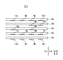
- FIG. 2 to 5 are cross-sectional structural views of the multilayer substrate 10a when it is manufactured.
- FIG. 6 is a cross-sectional structure diagram of the multilayer substrate 10a when a large amount of conductive paste is applied.
- a case where one multilayer substrate 10a is manufactured will be described as an example, but actually, a plurality of multilayer substrates 10a are manufactured simultaneously by laminating and cutting large-sized insulator sheets.
- insulator sheets 16a to 16e made of a thermoplastic resin such as a liquid crystal polymer are prepared.
- a copper foil is formed on the entire main surface of one of the insulator sheets 16a to 16e.
- copper foil is attached to the back surfaces of the insulator sheets 16a to 16e.
- the surface of the copper foil of the insulating sheets 16a to 16e is smoothed by, for example, applying a zinc plating for rust prevention.
- metal foils other than copper foil may be used.
- wiring conductor layers 18a to 18d are formed on the back surface of the insulator sheet 16a as shown in FIG. Specifically, a resist having the same shape as that of the wiring conductor layers 18a to 18d shown in FIG. 2 is printed on the copper foil on the back surface of the insulator sheet 16a. And the copper foil of the part which is not covered with the resist is removed by performing an etching process with respect to copper foil. Thereafter, the resist is removed by spraying a cleaning liquid (resist removing liquid). As a result, wiring conductor layers 18a to 18d as shown in FIG. 2 are formed on the back surface of the insulator sheet 16a by a photolithography process.
- a cleaning liquid resist removing liquid
- wiring conductor layers 18e to 18p are formed on the back surfaces of the insulating sheets 16b to 16e, respectively. Note that the formation process of the wiring conductor layers 18e to 18p is the same as the formation process of the wiring conductor layers 18a to 18d, and a description thereof will be omitted.
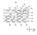
- a plurality of through holes h1 to h11 are formed in the insulator sheets 16a to 16e (through hole forming step). More specifically, a laser beam is irradiated from the surface side of the insulating sheets 16a to 16e to the positions where the via hole conductors v1 to v11 of the insulating sheets 16a to 16e are formed.
- a Cu—Sn based conductive paste is applied to the plurality of through holes h1 to h11 by screen printing (paste applying step).
- paste applying step a Cu—Sn based conductive paste is applied to the plurality of through holes h1 to h11 by screen printing (paste applying step).
- the position where the most via-hole conductors are located is the position Pc (an example of the first position).
- Five via-hole conductors v1, v3, v5, v7, v10 are located at the position Pc.
- the through holes corresponding to the via-hole conductors v1, v3, v5, v7, v10 are through holes h1, h3, h5, h7, h10.
- the position where the fewest via hole conductors are located is a position Pb (an example of the second position).
- One via-hole conductor v9 (an example of a second via-hole conductor) is located at the position Pb.
- the through hole corresponding to the via hole conductor v9 is a through hole h9.
- the ratio of the volume of the conductive paste applied to the through holes h1, h3, h5, h7, h10 to the volume of the through holes h1, h3, h5, h7, h10 is The conductive paste is applied to the through holes h1 to h11 so that the volume of the conductive paste applied to the through holes h9 and h11 is lower than the ratio of the volume of the conductive paste to the through holes h9 and h11.
- the ratio of the volume of the conductive paste applied to the through holes h1, h3, h5, h7, h10 to the volume of the through holes h1, h3, h5, h7, h10 Defined as the application rate of the through holes h1, h3, h5, h7, h10.
- the application rate of the through holes h1, h3, h5, h7, h10 is lower than the application rate of the remaining through holes h2, h4, h6, h8, h9, h11.
- the volume of the through hole and the volume of the conductive paste applied to the through hole will be described.
- the volume of the through hole is the inner peripheral surface Sa of the through hole, the virtual surface Sb in which the surface of the insulator sheet is extended to the through hole, and the back surface of the insulator sheet is extended to the through hole. This is the volume of the space surrounded by the virtual surface Sc.
- the volume of the conductive paste is the volume of the conductive paste filled in the through holes.
- the conductive paste sometimes protrudes upward from the through hole.
- the volume of the conductive paste is the sum of the volume of the conductive paste filled in the through hole and the volume of the conductive paste protruding upward from the through hole.
- changing the application rate of the through holes can be realized by adjusting the printing conditions.
- adjusting the printing conditions for example, the number of times of applying the conductive paste to the through holes h1, h3, h5, h7, h10 is applied to the remaining through holes h2, h4, h6, h8, h9, h11.
- the number may be larger than the number of times to be performed.
- coating rate of a through-hole can also be adjusted by adjusting the angle of a squeegee and a screen board when apply
- the application rate of a through-hole can be adjusted also by adjusting the moving speed of the squeegee at the time of apply
- the insulating sheets 16a to 16e are laminated and pressure-bonded (laminated pressure bonding step). Specifically, as shown in FIG. 5, after the insulator sheets 16a to 16e are stacked, the insulator sheets 16a to 16e are subjected to pressure treatment and heat treatment (that is, thermocompression bonding). The pressurizing process is performed by sandwiching the insulating sheets 16a to 16e from above and below. By applying pressure treatment and heat treatment to the insulating sheets 16a to 16e, the insulating sheets 16a to 16e are softened and the conductive paste in the through holes is solidified. As a result, the insulator sheets 16a to 16e are joined and the via-hole conductors v1 to v11 are formed.
- pressure treatment and heat treatment that is, thermocompression bonding
- a protective layer is formed on the surface of the insulating sheet 16a by applying a resin (resist) paste by screen printing.
- the multilayer substrate 10a is completed through the above steps.
- the manufacturing method of the multilayer substrate 10a according to the present embodiment it is possible to suppress the deterioration of the flatness of the front surface and the back surface. More specifically, in the multilayer substrate 10a, the position where the most via-hole conductors are located when viewed from above is the position Pc. There is a possibility that the front surface and the back surface of the multilayer substrate 10a protrude above and below the position Pc. On the other hand, when viewed from above, the position where the fewest via hole conductors are located is the position Pb. Therefore, it is unlikely that the front and back surfaces of the multilayer substrate 10a protrude above and below the position Pb.
- the conductive paste is applied to the through holes h1 to h11 so that the application rate of the through holes h1, h3, h5, h7, h10 is lower than the application rate of the through hole h9. Is granted.
- the through holes h1, h3, h5, h7, and h10 are through holes corresponding to the via hole conductors v1, v3, v5, v7, and v10 located at the position Pc where the most via hole conductors are located.
- the through hole h9 is a through hole corresponding to the via hole conductor v9 located at the position Pb where the smallest number of via hole conductors are located.
- the application rate of the through holes h1, h3, h5, h7, h10 is lowered, and the thickness of the multilayer substrate body 12 at the position Pc approaches the thickness of the multilayer substrate body 12 at portions other than the position Pc.
- the manufacturing method of the multilayer substrate 10a it is possible to suppress the deterioration of the flatness of the front surface and the back surface.
- the application rate of the through holes h1, h3, h5, h7, h10 is lower than the application rate of the remaining through holes h2, h4, h6, h8, h9, h11.
- a conductive paste is applied to the through holes h1 to h11.
- the application rate of the through holes h1, h3, h5, h7, h10 is further reduced, and the thickness of the multilayer substrate body 12 at the position Pc approaches the thickness of the multilayer substrate body 12 at portions other than the position Pc. .
- deterioration of the flatness of the front surface and the back surface can be further suppressed.
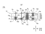
- FIG. 7 is a cross-sectional structure diagram of a multilayer substrate 10b according to a first modification of the present invention.
- the multilayer substrate 10b is different from the multilayer substrate 10a in the diameters of the via-hole conductors v1, v3, v5, v7, and v10.
- the multilayer substrate 10b will be described focusing on such differences.
- the diameters of the via-hole conductors v1 to v11 are equal to each other.
- the diameters of the via-hole conductors v1, v3, v5, v7, v10 are larger than the diameters of the via-hole conductors v2, v4, v6, v8, v9, v11 including the via-hole conductors v9, v11.
- FIG. 8 to 11 are cross-sectional structural views of the multilayer substrate 10b when it is manufactured.
- the process of forming the wiring conductor layers 18a to 18p in the multilayer board 10b is the same as the process of forming the wiring conductor layers 18a to 18p in the multilayer board 10a, as shown in FIGS.
- a plurality of through holes h1 to h11 are formed in the insulating sheets 16a to 16e (through hole forming step). More specifically, a laser beam is irradiated from the surface side of the insulating sheets 16a to 16e to the positions where the via hole conductors v1 to v11 of the insulating sheets 16a to 16e are formed.
- the diameters of the through holes h1, h3, h5, h7, and h10 are larger than the diameters of the through holes h2, h4, h6, h8, h9, and h11.
- the diameter of the laser beam when forming the through holes h1, h3, h5, h7, and h10 is larger than the diameter of the laser beam when forming the through holes h2, h4, h6, h8, h9, and h11.
- the number of irradiation times and time of the laser beam when forming the through holes h1, h3, h5, h7, and h10 are the number of times and time of laser beam irradiation when forming the through holes h2, h4, h6, h8, h9, and h11. It may be more.
- a conductive paste is applied to the plurality of through holes h1 to h11 by screen printing (paste application step).
- the diameters of the through holes h1, h3, h5, h7, h10 are larger than the diameters of the through holes h2, h4, h6, h8, h9, h11. Therefore, when the conductive paste is applied to the through holes h1 to h11 by screen printing at the same time under the same conditions, the amount of the conductive paste filled in the through holes h1, h3, h5, h7, h10 is reduced to the through holes h2, h2. It becomes larger than the amount of the conductive paste filled in h4, h6, h8, h9, and h11.
- the application rate of the through holes h1, h3, h5, h7, h10 is lower than the application rate of the through holes h2, h4, h6, h8, h9, h11 including the through holes h9, h11.
- the process of laminating and crimping the insulator sheets 16a to 16e in the multilayer substrate 10b is the same as the process of laminating and crimping the insulator sheets 16a to 16e in the multilayer substrate 10a as shown in FIGS. Is omitted.
- a protective layer is formed on the surface of the insulating sheet 16a by applying a resin (resist) paste by screen printing.
- the multilayer substrate 10b is completed through the above steps.
- the application rate of the through holes h1, h3, h5, h7, h10 is lower than the application rate of the remaining through holes h2, h4, h6, h8, h9, h11. Therefore, the via hole conductor with the smallest application rate of the through holes h1, h3, h5, h7, h10 corresponding to the via hole conductors v1, v3, v5, v7, v10 located at the position Pc where the most via hole conductors are located. This is lower than the application rate of the through-hole h9 corresponding to the via-hole conductor v9 located at the position Pb where is located.
- the diameters of the through holes h1, h3, h5, h7, h10 are larger than the diameters of the through holes h2, h4, h6, h8, h9, h11.
- the printing conditions for applying the conductive paste to the through holes h1, h3, h5, h7, h10 and the printing conditions for applying the conductive paste to the through holes h2, h4, h6, h8, h9, h11 are the same. Even in this case, the application rate of the through holes h1, h3, h5, h7, h10 can be made lower than the application rate of the through holes h2, h4, h6, h8, h9, h11.
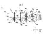
- FIG. 12 is a sectional structural view of a multilayer substrate 10c according to a second modification of the present invention.
- the multilayer substrate 10c is different from the multilayer substrate 10a in that the via-hole conductor v5 is not provided.
- the multilayer substrate 10c will be described focusing on the difference.
- the position where the via-hole conductors v6 and v8 are located when viewed from above is defined as a position Pa.
- a position where the via-hole conductor v9 is located when viewed from above is defined as a position Pb.
- a position where the via-hole conductors v1, v3, v7, v10 are located when viewed from above is defined as a position Pc.
- a position where the via-hole conductors v2, v4, v11 are located when viewed from above is defined as a position Pd.
- the via-hole conductors v1, v3, v5, v7, and v10 are connected to one at the position Pc where the most via-hole conductors are located.
- the via-hole conductors v1 and v3 are connected to one, and the via-hole conductors v7 and v10 are connected to one. That is, all the via-hole conductors located at the position Pc may not be connected to one. That is, when viewed from above, the deterioration of the flatness of the front surface and the back surface can be suppressed by reducing the application rate of the conductive paste to the through holes where the most via-hole conductors are located.
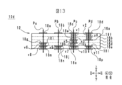
- FIG. 13 is a sectional structural view of a multilayer substrate 10d according to a third modification of the present invention.
- the multilayer substrate 10d is different from the multilayer substrate 10a in that the via-hole conductors v1, v3, v5, v7, v10 are not aligned in the vertical direction.
- the multilayer substrate 10d will be described focusing on such differences.
- the via-hole conductors v1, v3, v5, v7, v10 are slightly shifted in the left-right direction. As described above, the via-hole conductors v1, v3, v5, v7, and v10 may be connected to one, and may be slightly shifted from side to side. However, the via-hole conductors v1, v3, v5, v7, v10 have portions that overlap each other when viewed from above.
- the manufacturing method of the multilayer substrate 10d is the same as the manufacturing method of the multilayer substrate 10a, description thereof is omitted.
- the multilayer substrate and the method for manufacturing the multilayer substrate according to the present invention are not limited to the method for manufacturing the multilayer substrates 10a to 10d and the multilayer substrates 10a to 10d, and can be changed within the scope of the gist.
- the configurations of the manufacturing methods of the multilayer substrates 10a to 10d and the multilayer substrates 10a to 10d may be arbitrarily combined.
- the multilayer substrates 10a to 10d have flexibility, they may be multilayer substrates that do not have flexibility.
- the multilayer substrates 10a to 10d are preferably flexible substrates made of a thermoplastic resin or the like. This is because when the multilayer substrates 10a to 10d are flexible substrates made of a thermoplastic resin or the like, the via-hole conductor easily protrudes on the front surface or the back surface due to resin flow or the like in the crimping process.
- multilayer substrate 10a-10d has a three-dimensional structure. Therefore, the multilayer substrates 10a to 10d are provided with wiring conductor layers other than the wiring conductor layers 18a to 18p and via hole conductors other than the via hole conductors v1 to v11.
- the application rate is set lower than the application rate of the through hole h9 corresponding to the via hole conductor v9 located at the position Pb where the smallest via hole conductor is located.
- the method of changing the grant rate is not limited to this. At the position where many via-hole conductors are located, the flatness of the multilayer substrates 10a to 10d tends to deteriorate.
- the application rate to the through hole corresponding to the via-hole conductor may be changed according to the number of via-hole conductors. That is, as the number of via hole conductors increases, the rate of application to the through holes corresponding to the via hole conductors may be lowered.
- via hole conductors v1, v2, v3, v4, v5 located at a position Pc where the most via hole conductors are located and a position Pd where the second most via hole conductors are located.
- the present invention is useful for a multilayer substrate and a method for manufacturing the multilayer substrate, and is particularly excellent in that deterioration of flatness of the main surface can be suppressed.
- multilayer substrate 12 multilayer substrate body 16a to 16e: insulator sheets 18a to 18p: wiring conductor layers h1 to h11: through holes v1 to v11: via hole conductors
Landscapes
- Engineering & Computer Science (AREA)
- Microelectronics & Electronic Packaging (AREA)
- Manufacturing & Machinery (AREA)
- Production Of Multi-Layered Print Wiring Board (AREA)
Abstract
主面の平坦性の悪化を抑制できる多層基板及び多層基板の製造方法を提供する。 本発明に係る多層基板の製造方法は、絶縁体層に対してビアホール導体が形成される位置に貫通孔を形成する貫通孔形成工程と、貫通孔に対して導電性ペーストを付与するペースト付与工程と、を備えており、最も多くのビアホール導体が位置している位置を第1の位置とし、第1の位置に位置するビアホール導体を第1のビアホール導体とし、最も少ないビアホール導体が位置している位置を第2の位置とし、第2の位置に位置するビアホール導体を第2のビアホール導体とし、第1のビアホール導体に対応する貫通孔に付与される導電性ペーストの体積の貫通孔の体積に対する割合が、第2のビアホール導体に対応する貫通孔に付与される導電性ペーストの体積の貫通孔の体積に対する割合よりも低くなるように、導電性ペーストを付与すること、を特徴とする。
Description
本発明は、絶縁体層が積層されて構成された多層基板及び多層基板の製造方法に関する。
従来の多層基板に関する発明としては、例えば、特許文献1に記載の有機多層基板が知られている。図14は、特許文献1に記載の有機多層基板500の断面構造図である。
有機多層基板500は、積層体502及び複数のビアホール504を備えている。積層体502は、複数の樹脂シート層506が積層されて構成されている。複数のビアホール504は、樹脂シート層506を上下方向に貫通している。また、有機多層基板500では、図14の楕円で囲んだ部分のように、多くのビアホール504が一つに繋がって上下に重なっている。
ところで、特許文献1に記載の有機多層基板500では、多くのビアホール504が上下方向に重なっている部分において、主面の平坦性が悪化しやすい。より詳細には、有機多層基板500を形成する際には、樹脂シート層506に貫通孔を形成し、該貫通孔に導電性ペーストを充填する。そして、樹脂シート層506を積層・圧着することにより、有機多層基板500を得る。
ビアホール504は、他のビアホール504や導体層と接続される。ビアホール504と他のビアホール504又は導体層とが確実に接続されるように、貫通孔には多めに導電性ペーストが充填される。従って、図14の楕円で囲んだ部分のように、多くのビアホール504が上下方向に重なっている部分における積層体502の厚みは、残余の部分の積層体502の厚みよりも大きくなってしまう。その結果、有機多層基板500では、図14の拡大図のように、多くのビアホール504が重なっている部分において、主面が突出することによって主面の平坦性が悪化しやすい。主面の平坦性が悪化すると、例えば、有機多層基板500に電子部品を実装したり、有機多層基板500をマザー基板に実装したりする際に、実装不良が起こる可能性がある。
そこで、本発明の目的は、主面の平坦性の悪化を抑制できる多層基板及び多層基板の製造方法を提供することである。
本発明の一形態に係る多層基板の製造方法は、複数の絶縁体層に対して複数のビアホール導体が形成される位置に複数の貫通孔を形成する貫通孔形成工程と、前記複数の貫通孔に対して導電性ペーストを付与するペースト付与工程と、前記複数の絶縁体層を積層方向に積層し圧着する積層圧着工程と、を備えており、前記積層方向から見たときに、最も多くの前記ビアホール導体が位置している位置を第1の位置とし、該第1の位置に位置する前記ビアホール導体を第1のビアホール導体とし、前記積層方向から見たときに、最も少ない前記ビアホール導体が位置している位置を第2の位置とし、該第2の位置に位置する前記ビアホール導体を第2のビアホール導体とし、前記ペースト付与工程において、前記第1のビアホール導体に対応する前記貫通孔に付与される導電性ペーストの体積の該貫通孔の体積に対する割合が、前記第2のビアホール導体に対応する前記貫通孔に付与される導電性ペーストの体積の該貫通孔の体積に対する割合よりも低くなるように、前記複数の貫通孔に前記導電性ペーストを付与すること、を特徴とする。
本発明の一形態に係る多層基板は、複数の絶縁体層が積層方向に積層されて構成されている多層基板本体と、前記複数の絶縁体層を積層方向に貫通する複数のビアホール導体と、を備えており、前記積層方向から見たときに、最も多くの前記ビアホール導体が位置している位置を第1の位置とし、該第1の位置に位置する前記ビアホール導体を第1のビアホール導体とし、前記積層方向から見たときに、最も少ない前記ビアホール導体が位置している位置を第2の位置とし、該第2の位置に位置する前記ビアホール導体を第2のビアホール導体とし、前記第1のビアホール導体の径は、前記第2のビアホール導体の径よりも大きいこと、を特徴とする。
本発明によれば、主面の平坦性の悪化を抑制できる。
(実施形態)
<多層基板の構成>
以下に、本発明の一実施形態に係る多層基板10aの構成について図面を参照しながら説明する。図1は、本発明の一実施形態に係る多層基板10aの断面構造図である。以下では、多層基板10aの積層方向を上下方向(素体の主面の法線方向の一例)と定義する。また、図1の紙面の左右方向を左右方向と定義し、図1の紙面の前後方向を前後方向と定義する。上下方向、左右方向及び前後方向は互いに直交している。
<多層基板の構成>
以下に、本発明の一実施形態に係る多層基板10aの構成について図面を参照しながら説明する。図1は、本発明の一実施形態に係る多層基板10aの断面構造図である。以下では、多層基板10aの積層方向を上下方向(素体の主面の法線方向の一例)と定義する。また、図1の紙面の左右方向を左右方向と定義し、図1の紙面の前後方向を前後方向と定義する。上下方向、左右方向及び前後方向は互いに直交している。
多層基板10aは、例えば、携帯電話等の電子機器内に設けられ、表面及び裏面を有する長方形状の板状をなすフレキシブル基板である。多層基板10aは、図1に示すように、多層基板本体12、配線導体層18a~18p及びビアホール導体v1~v11を備えている。
多層基板本体12は、長方形状の板状をなしており、図1に示すように、絶縁体シート16a~16e(複数の絶縁体層の一例)が上側から下側へとこの順に積層されて構成されている。以下では、多層基板本体12の上側の主面を表面と称し、多層基板本体12の下側の主面を裏面と称す。
絶縁体シート16a~16eは、上側から見たときに、長方形状をなしており、多層基板本体12と同じ形状をなしている。絶縁体シート16a~16eは、ポリイミドや液晶ポリマ等の可撓性を有する熱可塑性樹脂により作製されている絶縁体層である。その他の熱可塑性樹脂の例としては、ポリエーテルエーテルケトン、ポリイミド、ポリエーテルイミド、ポリフェニレンスルファイド等が挙げられる。以下では、絶縁体シート16a~16eの上側の主面を表面と称し、絶縁体シート16a~16eの下側の主面を裏面と称す。
配線導体層18a~18dは、絶縁体シート16aの表面に設けられており、左側から右側へとこの順に並んでいる。配線導体層18e,18fは、絶縁体シート16bの裏面に設けられており、左側から右側へとこの順に並んでいる。配線導体層18g,18hは、絶縁体シート16cの裏面に設けられており、左側から右側へとこの順に並んでいる。配線導体層18i~18lは、絶縁体シート16dの裏面に設けられており、左側から右側へとこの順に並んでいる。配線導体層18m~18pは、絶縁体シート16eの裏面に設けられており、左側から右側へとこの順に並んでいる。
配線導体層18a,18g,18i,18mは、上側から見たときに、重なっている部分を有する。配線導体層18b,18j,18nは、上側から見たときに、重なっている部分を有する。配線導体層18c,18e,18h,18k,18oは、上側から見たときに、重なっている部分を有する。配線導体層18d,18f,18l,18pは、上側から見たときに、重なっている部分を有する。
配線導体層18a~18dは、外部電極として機能する。具体的には、多層基板10aの表面上には電子部品が実装される。この際、電子部品の外部電極と多層基板10aの配線導体層18a~18dとがはんだにより接合される。
配線導体層18m~18pは、外部電極として機能する。具体的には、多層基板10aはマザー基板に実装される。この際、マザー基板の外部電極と多層基板10aの配線導体層18m~18pとがはんだにより接合される。
以上のような配線導体層18a~18pは、銅箔等の金属箔により構成されている。
ビアホール導体v1,v2は、絶縁体シート16aを上下方向に貫通しており、左側から右側へとこの順に並んでいる。ビアホール導体v3,v4は、絶縁体シート16bを上下方向に貫通しており、左側から右側へとこの順に並んでいる。ビアホール導体v5は、絶縁体シート16cを上下方向に貫通している。ビアホール導体v6,v7は、絶縁体シート16dを上下方向に貫通しており、左側から右側へとこの順に並んでいる。ビアホール導体v8~v11は、絶縁体シート16eを上下方向に貫通しており、左側から右側へとこの順に並んでいる。
ビアホール導体v6,v8は、一つに繋がっており、配線導体層18g,18i,18mを接続している。ビアホール導体v9は、配線導体層18j,18nを接続している。ビアホール導体v1,v3,v5,v7,v10は、一つに繋がっており、配線導体層18c,18e,18h,18k,18oを接続している。ビアホール導体v2,v4は、一つに繋がっており、配線導体層18d,18fを接続している。ビアホール導体v11は、配線導体層18l,18pを接続している。
また、上側から見たときに、ビアホール導体v6,v8が位置している位置を位置Paと定義する。上側から見たときに、ビアホール導体v9が位置している位置を位置Pbと定義する。上側から見たときに、ビアホール導体v1,v3,v5,v7,v10が位置している位置を位置Pcと定義する。上側から見たときに、ビアホール導体v2,v4,v11が位置している位置を位置Pdと定義する。
以上のようなビアホール導体v1~v11は、例えば、Cu-Sn系の導電性ペーストが焼結されることにより形成される。
<多層基板の製造方法>
以下に、多層基板10aの製造方法について図面を参照しながら説明する。図2ないし図5は、多層基板10aの製造時の断面構造図である。図6は、導電性ペーストが多く付与された場合の多層基板10aの製造時の断面構造図である。以下では、一つの多層基板10aが作製される場合を例にとって説明するが、実際には、大判の絶縁体シートが積層及びカットされることにより、同時に複数の多層基板10aが作製される。
以下に、多層基板10aの製造方法について図面を参照しながら説明する。図2ないし図5は、多層基板10aの製造時の断面構造図である。図6は、導電性ペーストが多く付与された場合の多層基板10aの製造時の断面構造図である。以下では、一つの多層基板10aが作製される場合を例にとって説明するが、実際には、大判の絶縁体シートが積層及びカットされることにより、同時に複数の多層基板10aが作製される。
まず、液晶ポリマ等の熱可塑性樹脂により作製された絶縁体シート16a~16eを準備する。次に、絶縁体シート16a~16eの一方の主面の全面に銅箔を形成する。具体的には、絶縁体シート16a~16eの裏面に銅箔を張り付ける。更に、絶縁体シート16a~16eの銅箔の表面に、例えば、防錆のための亜鉛鍍金を施して、平滑化する。なお、銅箔以外の金属箔が用いられてもよい。
次に、絶縁体シート16aの裏面上に形成された銅箔をパターニングすることにより、図2に示すように、配線導体層18a~18dを絶縁体シート16aの裏面上に形成する。具体的には、絶縁体シート16aの裏面の銅箔上に、図2に示す配線導体層18a~18dと同じ形状のレジストを印刷する。そして、銅箔に対してエッチング処理を施すことにより、レジストにより覆われていない部分の銅箔を除去する。その後、洗浄液(レジスト除去液)を吹き付けてレジストを除去する。これにより、図2に示すような、配線導体層18a~18dが絶縁体シート16aの裏面上にフォトリソグラフィ工程により形成される。
次に、図2に示すように、配線導体層18e~18pを絶縁体シート16b~16eの裏面上にそれぞれ形成する。なお、配線導体層18e~18pの形成工程は、配線導体層18a~18dの形成工程と同じであるので説明を省略する。
次に、図3に示すように、絶縁体シート16a~16eに対して複数の貫通孔h1~h11を形成する(貫通孔形成工程)。より詳細には、絶縁体シート16a~16eのビアホール導体v1~v11が形成される位置に、絶縁体シート16a~16eの表面側からレーザービームを照射する。
次に、図4に示すように、スクリーン印刷により、複数の貫通孔h1~h11に対して、Cu-Sn系の導電性ペーストを付与する(ペースト付与工程)。以下に、ペースト付与工程についてより詳細に説明する。
図1に示すように、上側から見たときに、最も多くのビアホール導体が位置している位置は、位置Pc(第1の位置の一例)である。位置Pcには、5個のビアホール導体v1,v3,v5,v7,v10(第1のビアホール導体の一例)が位置している。また、ビアホール導体v1,v3,v5,v7,v10に対応する貫通孔は、貫通孔h1,h3,h5,h7,h10である。
また、図1に示すように、上側から見たときに、最も少ないビアホール導体が位置している位置は、位置Pb(第2の位置の一例)である。位置Pbには、1個のビアホール導体v9(第2のビアホール導体の一例)が位置している。また、ビアホール導体v9に対応する貫通孔は、貫通孔h9である。
ペースト付与工程では、図4に示すように、貫通孔h1,h3,h5,h7,h10に付与される導電性ペーストの体積の貫通孔h1,h3,h5,h7,h10の体積に対する割合が、貫通孔h9,h11に付与される導電性ペーストの体積の貫通孔h9,h11の体積に対する割合よりも低くなるように、貫通孔h1~h11に導電性ペーストを付与する。以下では、説明の簡素化のために、例えば、貫通孔h1,h3,h5,h7,h10に付与される導電性ペーストの体積の貫通孔h1,h3,h5,h7,h10の体積に対する割合を、貫通孔h1,h3,h5,h7,h10の付与率と定義する。本実施形態では、貫通孔h1,h3,h5,h7,h10の付与率は、残余の貫通孔h2,h4,h6,h8,h9,h11の付与率よりも低い。
ここで、貫通孔の体積、及び、貫通孔に付与される導電性ペーストの体積について説明する。貫通孔の体積とは、図3に示すように、貫通孔の内周面Sa、絶縁体シートの表面を貫通孔まで伸ばした仮想面Sb、及び、絶縁体シートの裏面を貫通孔まで伸ばした仮想面Scにより囲まれた空間の体積である。導電性ペーストの体積とは、貫通孔内に充填されている導電ペーストの体積である。ただし、図6に示すように、導電性ペーストが貫通孔から上側にはみ出す場合がある。このような場合には、導電性ペーストの体積は、貫通孔内に充填されている導電ペーストの体積及び貫通孔から上側にはみ出している導電性ペーストの体積の合計である。
前記のように、貫通孔の付与率を変化させることは、印刷条件を調整することによって実現可能である。印刷条件の調整例としては、例えば、貫通孔h1,h3,h5,h7,h10に導電ペーストを付与する回数を残余の貫通孔h2,h4,h6,h8,h9,h11に導電性ペーストを付与する回数よりも多くする等が挙げられる。また、導電性ペーストを塗布する際にスキージとスクリーン板との角度を調整することによっても、貫通孔の付与率を調整できる。具体的には、スキージとスクリーン板との角度が大きくなると、貫通孔の付与率が小さくなる。また、導電性ペーストを塗布する際のスキージの移動速度を調整することによっても、貫通孔の付与率を調整できる。具体的には、スキージの移動速度が大きくなれば、貫通孔の付与率が小さくなる。
次に、図5に示すように、絶縁体シート16aの表裏を反転させる。
次に、図1に示すように、絶縁体シート16a~16eを積層し圧着する(積層圧着工程)。具体的には、図5に示すように、絶縁体シート16a~16eを積層した後、絶縁体シート16a~16eに対して加圧処理及び加熱処理(すなわち、熱圧着)を施す。加圧処理は、上下方向から絶縁体シート16a~16eを挟むことにより行う。絶縁体シート16a~16eに対して加圧処理及び加熱処理が施されることにより、絶縁体シート16a~16eが軟化すると共に、貫通孔内の導電性ペーストが固化する。これにより、絶縁体シート16a~16eが接合されると共に、ビアホール導体v1~v11が形成される。
次に、必要に応じて、樹脂(レジスト)ペーストをスクリーン印刷により塗布することにより、絶縁体シート16aの表面上に保護層を形成する。以上の工程を経て、多層基板10aが完成する。
<効果>
本実施形態に係る多層基板10aの製造方法によれば、表面及び裏面の平坦性の悪化を抑制できる。より詳細には、多層基板10aにおいて、上側から見たときに、最も多くのビアホール導体が位置している位置は、位置Pcである。位置Pcの上側及び下側において、多層基板10aの表面及び裏面が突出する可能性がある。一方、上側から見たときに、最も少ないビアホール導体が位置している位置は、位置Pbである。そのため、位置Pbの上側及び下側において、多層基板10aの表面及び裏面が突出する可能性は低い。
本実施形態に係る多層基板10aの製造方法によれば、表面及び裏面の平坦性の悪化を抑制できる。より詳細には、多層基板10aにおいて、上側から見たときに、最も多くのビアホール導体が位置している位置は、位置Pcである。位置Pcの上側及び下側において、多層基板10aの表面及び裏面が突出する可能性がある。一方、上側から見たときに、最も少ないビアホール導体が位置している位置は、位置Pbである。そのため、位置Pbの上側及び下側において、多層基板10aの表面及び裏面が突出する可能性は低い。
そこで、多層基板10aでは、ペースト付与工程において、貫通孔h1,h3,h5,h7,h10の付与率が、貫通孔h9の付与率よりも低くなるように、貫通孔h1~h11に導電性ペーストを付与する。貫通孔h1,h3,h5,h7,h10は、最も多くのビアホール導体が位置している位置Pcに位置するビアホール導体v1,v3,v5,v7,v10に対応する貫通孔である。貫通孔h9は、最も少ないビアホール導体が位置している位置Pbに位置するビアホール導体v9に対応する貫通孔である。これにより、貫通孔h1,h3,h5,h7,h10の付与率が低くなり、位置Pcにおける多層基板本体12の厚みが、位置Pc以外の部分における多層基板本体12の厚みに近づくようになる。その結果、多層基板10aの製造方法によれば、表面及び裏面の平坦性の悪化を抑制できる。
また、多層基板10aでは、ペースト付与工程において、貫通孔h1,h3,h5,h7,h10の付与率が、残余の貫通孔h2,h4,h6,h8,h9,h11の付与率よりも低くなるように、貫通孔h1~h11に導電性ペーストを付与する。これにより、貫通孔h1,h3,h5,h7,h10の付与率が更に低くなり、位置Pcにおける多層基板本体12の厚みが、位置Pc以外の部分における多層基板本体12の厚みに近づくようになる。その結果、多層基板10aの製造方法によれば、表面及び裏面の平坦性の悪化をより抑制できる。
(第1の変形例)
<多層基板の構成>
以下に、本発明の第1の変形例に係る多層基板10bの構成について図面を参照しながら説明する。図7は、本発明の第1の変形例に係る多層基板10bの断面構造図である。
<多層基板の構成>
以下に、本発明の第1の変形例に係る多層基板10bの構成について図面を参照しながら説明する。図7は、本発明の第1の変形例に係る多層基板10bの断面構造図である。
多層基板10bは、ビアホール導体v1,v3,v5,v7,v10の径において多層基板10aと相違する。以下、かかる相違点を中心に多層基板10bについて説明する。
多層基板10aでは、ビアホール導体v1~v11の径は互いに等しい。一方、多層基板10bでは、ビアホール導体v1,v3,v5,v7,v10の径は、ビアホール導体v9,v11を含むビアホール導体v2,v4,v6,v8,v9,v11の径よりも大きい。
<多層基板の製造方法>
以下に、多層基板10bの製造方法について図面を参照しながら説明する。図8~図11は、多層基板10bの製造時の断面構造図である。
以下に、多層基板10bの製造方法について図面を参照しながら説明する。図8~図11は、多層基板10bの製造時の断面構造図である。
多層基板10bにおける配線導体層18a~18pを形成する工程は、図2及び図8に示すように、多層基板10aにおける配線導体層18a~18pを形成する工程と同じであるので説明を省略する。
次に、図9に示すように、絶縁体シート16a~16eに対して複数の貫通孔h1~h11を形成する(貫通孔形成工程)。より詳細には、絶縁体シート16a~16eのビアホール導体v1~v11が形成される位置に、絶縁体シート16a~16eの表面側からレーザービームを照射する。ただし、貫通孔h1,h3,h5,h7,h10の径は、貫通孔h2,h4,h6,h8,h9,h11の径よりも大きい。そこで、貫通孔h1,h3,h5,h7,h10の形成時のレーザービームの径は、貫通孔h2,h4,h6,h8,h9,h11の形成時のレーザービームの径よりも大きい。なお、貫通孔h1,h3,h5,h7,h10の形成時のレーザービームの照射回数や時間を、貫通孔h2,h4,h6,h8,h9,h11の形成時のレーザービームの照射回数や時間より多くしてもよい。
次に、図10に示すように、スクリーン印刷により、複数の貫通孔h1~h11に対して導電性ペーストを付与する(ペースト付与工程)。貫通孔h1,h3,h5,h7,h10の径は、貫通孔h2,h4,h6,h8,h9,h11の径よりも大きい。そのため、貫通孔h1~h11に対して同条件で同時にスクリーン印刷により導電性ペーストを付与すると、貫通孔h1,h3,h5,h7,h10において充填される導電性ペーストの量が、貫通孔h2,h4,h6,h8,h9,h11において充填される導電性ペーストの量よりも多くなる。その結果、貫通孔h1,h3,h5,h7,h10の付与率は、貫通孔h9,h11を含む貫通孔h2,h4,h6,h8,h9,h11の付与率よりも低くなる。
次に、図11に示すように、絶縁体シート16aの表裏を反転させる。
多層基板10bにおける絶縁体シート16a~16eを積層し圧着する工程は、図1及び図7に示すように、多層基板10aにおける絶縁体シート16a~16eを積層し圧着する工程と同じであるので説明を省略する。
次に、必要に応じて、樹脂(レジスト)ペーストをスクリーン印刷により塗布することにより、絶縁体シート16aの表面上に保護層を形成する。以上の工程を経て、多層基板10bが完成する。
このようにして得られた多層基板10bでは、貫通孔h1,h3,h5,h7,h10の付与率が残余の貫通孔h2,h4,h6,h8,h9,h11の付与率よりも低くなる。よって、最も多くビアホール導体が位置している位置Pcに位置するビアホール導体v1,v3,v5,v7,v10に対応する貫通孔h1,h3,h5,h7,h10の付与率が、最も少ないビアホール導体が位置している位置Pbに位置するビアホール導体v9に対応する貫通孔h9の付与率よりも低くなる。
<効果>
本実施形態に係る多層基板10bの製造方法によれば、多層基板10aの製造方法と同じ作用効果を奏することができる。
本実施形態に係る多層基板10bの製造方法によれば、多層基板10aの製造方法と同じ作用効果を奏することができる。
また、多層基板10bの製造方法では、貫通孔h1,h3,h5,h7,h10の径は、貫通孔h2,h4,h6,h8,h9,h11の径よりも大きい。これにより、貫通孔h1,h3,h5,h7,h10に導電性ペーストを付与する印刷条件と貫通孔h2,h4,h6,h8,h9,h11に導電性ペーストを付与する印刷条件とを同じにした場合であっても、貫通孔h1,h3,h5,h7,h10の付与率を貫通孔h2,h4,h6,h8,h9,h11の付与率よりも低くできる。
(第2の変形例)
<多層基板の構成>
以下に、本発明の第2の変形例に係る多層基板10cの構成について図面を参照しながら説明する。図12は、本発明の第2の変形例に係る多層基板10cの断面構造図である。
<多層基板の構成>
以下に、本発明の第2の変形例に係る多層基板10cの構成について図面を参照しながら説明する。図12は、本発明の第2の変形例に係る多層基板10cの断面構造図である。
多層基板10cは、ビアホール導体v5が設けられていない点において多層基板10aと相違する。以下、かかる相違点を中心に多層基板10cについて説明する。
上側から見たときに、ビアホール導体v6,v8が位置している位置を位置Paと定義する。上側から見たときに、ビアホール導体v9が位置している位置を位置Pbと定義する。上側から見たときに、ビアホール導体v1,v3,v7,v10が位置している位置を位置Pcと定義する。上側から見たときに、ビアホール導体v2,v4,v11が位置している位置を位置Pdと定義する。
以上のように、多層基板10aでは、最も多くのビアホール導体が位置している位置Pcでは、ビアホール導体v1,v3,v5,v7,v10が一つに繋がっている。一方、多層基板10cでは、位置Pcでは、ビアホール導体v1,v3が一つに繋がっており、ビアホール導体v7,v10が一つに繋がっている。すなわち、位置Pcに位置する全てのビアホール導体が一つに繋がっていなくてもよい。すなわち、上側から見たときに、最も多くのビアホール導体が位置する貫通孔への導電性ペーストの付与率を低くすることにより、表面及び裏面の平坦性の悪化を抑制できる。
(第3の変形例)
以下に、本発明の第3の変形例に係る多層基板10dの構成について図面を参照しながら説明する。図13は、本発明の第3の変形例に係る多層基板10dの断面構造図である。
以下に、本発明の第3の変形例に係る多層基板10dの構成について図面を参照しながら説明する。図13は、本発明の第3の変形例に係る多層基板10dの断面構造図である。
多層基板10dは、ビアホール導体v1,v3,v5,v7,v10が上下方向に一列に並んでいない点において多層基板10aと相違する。以下、かかる相違点を中心に多層基板10dについて説明する。
多層基板10dでは、ビアホール導体v1,v3,v5,v7,v10は、左右方向にわずかにずれている。このように、ビアホール導体v1,v3,v5,v7,v10は、一つに繋がっていればよく、左右にわずかにずれていてもよい。ただし、ビアホール導体v1,v3,v5,v7,v10は、上側から見たときに、互いに重なり合う部分を有する。
多層基板10dの製造方法は、多層基板10aの製造方法と同じであるので説明を省略する。
(その他の実施形態)
本発明に係る多層基板及び多層基板の製造方法は、前記多層基板10a~10d及び多層基板10a~10dの製造方法に限らず、その要旨の範囲内において変更可能である。
本発明に係る多層基板及び多層基板の製造方法は、前記多層基板10a~10d及び多層基板10a~10dの製造方法に限らず、その要旨の範囲内において変更可能である。
また、多層基板10a~10d及び多層基板10a~10dの製造方法の各構成を任意に組み合わせてもよい。
なお、多層基板10a~10dは、可撓性を有するものとしたが、可撓性を有さない多層基板であってもよい。ただし、多層基板10a~10dは、熱可塑性樹脂等により作製された可撓性を有する基板であることが好ましい。これは、多層基板10a~10dが熱可塑性樹脂等により作製された可撓性を有する基板である場合には、圧着工程において、樹脂流動等によりビアホール導体が表面又は裏面において突出し易いためである。
なお、多層基板10a~10dの2次元の断面構造図を用いて説明したが、実際には、多層基板10a~10dは3次元構造を有している。そのため、多層基板10a~10dには、配線導体層18a~18p以外の配線導体層やビアホール導体v1~v11以外のビアホール導体が設けられている。
なお、多層基板10a~10dでは、最も多くのビアホール導体が位置している位置Pcに位置するビアホール導体v1,v3,v5,v7,v10に対応する貫通孔h1,h3,h5,h7,h10の付与率を最も少ないビアホール導体が位置している位置Pbに位置するビアホール導体v9に対応する貫通孔h9の付与率よりも低くしている。しかしながら、付与率の変化のさせ方はこれに限らない。多くのビアホール導体が位置している位置では、多層基板10a~10dの平坦性が悪化しやすい。そこで、ビアホール導体が位置している数に応じて、該ビアホール導体に対応する貫通孔への付与率を変化させてもよい。すなわち、ビアホール導体が位置している数が多くなるにしたがって、該ビアホール導体に対応する貫通孔への付与率を低くしてもよい。他の例としては、例えば、最も多くのビアホール導体が位置している位置Pc及び2番目に多くのビアホール導体が位置している位置Pdに位置するビアホール導体v1,v2,v3,v4,v5,v7,v10,v11に対応する貫通孔h1,h2,h3,h4,h5,h7,h10,h11の付与率を、残余の貫通孔h6,h8,h9の付与率よりも低くしてもよい。
以上のように、本発明は、多層基板及び多層基板の製造方法に有用であり、特に、主面の平坦性の悪化を抑制できる点において優れている。
10a~10d:多層基板
12:多層基板本体
16a~16e:絶縁体シート
18a~18p:配線導体層
h1~h11:貫通孔
v1~v11:ビアホール導体
12:多層基板本体
16a~16e:絶縁体シート
18a~18p:配線導体層
h1~h11:貫通孔
v1~v11:ビアホール導体
Claims (5)
- 複数の絶縁体層に対して複数のビアホール導体が形成される位置に複数の貫通孔を形成する貫通孔形成工程と、
前記複数の貫通孔に対して導電性ペーストを付与するペースト付与工程と、
前記複数の絶縁体層を積層方向に積層し圧着する積層圧着工程と、
を備えており、
前記積層方向から見たときに、最も多くの前記ビアホール導体が位置している位置を第1の位置とし、該第1の位置に位置する前記ビアホール導体を第1のビアホール導体とし、
前記積層方向から見たときに、最も少ない前記ビアホール導体が位置している位置を第2の位置とし、該第2の位置に位置する前記ビアホール導体を第2のビアホール導体とし、
前記ペースト付与工程において、前記第1のビアホール導体に対応する前記貫通孔に付与される導電性ペーストの体積の該貫通孔の体積に対する割合が、前記第2のビアホール導体に対応する前記貫通孔に付与される導電性ペーストの体積の該貫通孔の体積に対する割合よりも低くなるように、前記複数の貫通孔に前記導電性ペーストを付与すること、
を特徴とする多層基板の製造方法。 - 前記第1のビアホール導体に対応する前記貫通孔の径は、前記第2のビアホール導体に対応する前記貫通孔の径よりも大きいこと、
を特徴とする請求項1に記載の多層基板の製造方法。 - 前記複数の絶縁体層は、熱可塑性樹脂により構成されていること、
を特徴とする請求項1又は請求項2のいずれかに記載の多層基板の製造方法。 - 前記ペースト付与工程では、スクリーン印刷により、前記複数の貫通孔に対して前記導電性ペーストを付与すること、
を特徴とする請求項1ないし請求項3のいずれかに記載の多層基板の製造方法。 - 複数の絶縁体層が積層方向に積層されて構成されている多層基板本体と、
前記複数の絶縁体層を積層方向に貫通する複数のビアホール導体と、
を備えており、
前記積層方向から見たときに、最も多くの前記ビアホール導体が位置している位置を第1の位置とし、該第1の位置に位置する前記ビアホール導体を第1のビアホール導体とし、
前記積層方向から見たときに、最も少ない前記ビアホール導体が位置している位置を第2の位置とし、該第2の位置に位置する前記ビアホール導体を第2のビアホール導体とし、
前記第1のビアホール導体の径は、前記第2のビアホール導体の径よりも大きいこと、
を特徴とする多層基板。
Applications Claiming Priority (2)
| Application Number | Priority Date | Filing Date | Title |
|---|---|---|---|
| JP2015201687 | 2015-10-13 | ||
| JP2015-201687 | 2015-10-13 |
Publications (1)
| Publication Number | Publication Date |
|---|---|
| WO2017065012A1 true WO2017065012A1 (ja) | 2017-04-20 |
Family
ID=58517181
Family Applications (1)
| Application Number | Title | Priority Date | Filing Date |
|---|---|---|---|
| PCT/JP2016/078760 Ceased WO2017065012A1 (ja) | 2015-10-13 | 2016-09-29 | 多層基板及び多層基板の製造方法 |
Country Status (1)
| Country | Link |
|---|---|
| WO (1) | WO2017065012A1 (ja) |
Citations (2)
| Publication number | Priority date | Publication date | Assignee | Title |
|---|---|---|---|---|
| JPH0818236A (ja) * | 1994-06-29 | 1996-01-19 | Kyocera Corp | 積層セラミック回路基板の製造方法 |
| JPH08274467A (ja) * | 1995-03-30 | 1996-10-18 | Mitsubishi Electric Corp | 多層セラミック基板のバイア形成方法 |
-
2016
- 2016-09-29 WO PCT/JP2016/078760 patent/WO2017065012A1/ja not_active Ceased
Patent Citations (2)
| Publication number | Priority date | Publication date | Assignee | Title |
|---|---|---|---|---|
| JPH0818236A (ja) * | 1994-06-29 | 1996-01-19 | Kyocera Corp | 積層セラミック回路基板の製造方法 |
| JPH08274467A (ja) * | 1995-03-30 | 1996-10-18 | Mitsubishi Electric Corp | 多層セラミック基板のバイア形成方法 |
Similar Documents
| Publication | Publication Date | Title |
|---|---|---|
| JP6149920B2 (ja) | リジッドフレキシブル基板およびその製造方法 | |
| TWI621388B (zh) | Method for manufacturing multilayer printed wiring board and multilayer printed wiring board | |
| KR101868680B1 (ko) | 회로 기판, 회로 기판의 제조 방법 및 전자 기기 | |
| US9179553B2 (en) | Method of manufacturing multilayer wiring board | |
| WO2017086095A1 (ja) | 多層基板及び電子機器 | |
| JP6436126B2 (ja) | 電子部品及び電子部品の製造方法 | |
| JP5684958B1 (ja) | プリント配線基板 | |
| WO2017026320A1 (ja) | 多層基板及びその製造方法 | |
| JP5118238B2 (ja) | 耐食性と歩留まりを向上させたプリント基板 | |
| KR102488164B1 (ko) | 프로파일된 도전성 층을 갖는 인쇄 회로 기판 및 그 제조 방법 | |
| WO2016013473A1 (ja) | プリント配線板及びその製造方法 | |
| US20130256010A1 (en) | Method of manufacturing multilayer printed circuit board and multilayer printed circuit board manufactured via the same | |
| WO2009131182A1 (ja) | フレックスリジッド配線基板とその製造方法 | |
| WO2012124421A1 (ja) | フレキシブル多層基板 | |
| US8586876B2 (en) | Laminated circuit board and board producing method | |
| JPWO2017065094A1 (ja) | 多層基板 | |
| JP2009010266A (ja) | プリント配線板の製造方法及びプリント配線板 | |
| WO2017119249A1 (ja) | 多層基板及び多層基板の製造方法 | |
| TWI580331B (zh) | 具有凹槽的多層線路板與其製作方法 | |
| WO2017065012A1 (ja) | 多層基板及び多層基板の製造方法 | |
| JP6315681B2 (ja) | 部品内蔵基板及びその製造方法並びに実装体 | |
| TWI461135B (zh) | 製作電路板之方法 | |
| JP6885422B2 (ja) | 樹脂基板および電子機器 | |
| CN111629513B (zh) | 同时具有贯孔及盲孔的多层电路板结构及其制法 | |
| JP2008258358A (ja) | リジッドフレキ基板とその製造方法 |
Legal Events
| Date | Code | Title | Description |
|---|---|---|---|
| 121 | Ep: the epo has been informed by wipo that ep was designated in this application |
Ref document number: 16855266 Country of ref document: EP Kind code of ref document: A1 |
|
| NENP | Non-entry into the national phase |
Ref country code: DE |
|
| 122 | Ep: pct application non-entry in european phase |
Ref document number: 16855266 Country of ref document: EP Kind code of ref document: A1 |
|
| NENP | Non-entry into the national phase |
Ref country code: JP |