WO2017061050A1 - 半導体装置 - Google Patents
半導体装置 Download PDFInfo
- Publication number
- WO2017061050A1 WO2017061050A1 PCT/JP2015/078821 JP2015078821W WO2017061050A1 WO 2017061050 A1 WO2017061050 A1 WO 2017061050A1 JP 2015078821 W JP2015078821 W JP 2015078821W WO 2017061050 A1 WO2017061050 A1 WO 2017061050A1
- Authority
- WO
- WIPO (PCT)
- Prior art keywords
- gate
- work function
- metal
- semiconductor layer
- semiconductor device
- Prior art date
- Legal status (The legal status is an assumption and is not a legal conclusion. Google has not performed a legal analysis and makes no representation as to the accuracy of the status listed.)
- Ceased
Links
Images



Classifications
-
- H—ELECTRICITY
- H10—SEMICONDUCTOR DEVICES; ELECTRIC SOLID-STATE DEVICES NOT OTHERWISE PROVIDED FOR
- H10D—INORGANIC ELECTRIC SEMICONDUCTOR DEVICES
- H10D64/00—Electrodes of devices having potential barriers
- H10D64/20—Electrodes characterised by their shapes, relative sizes or dispositions
- H10D64/27—Electrodes not carrying the current to be rectified, amplified, oscillated or switched, e.g. gates
- H10D64/311—Gate electrodes for field-effect devices
- H10D64/411—Gate electrodes for field-effect devices for FETs
- H10D64/511—Gate electrodes for field-effect devices for FETs for IGFETs
- H10D64/512—Disposition of the gate electrodes, e.g. buried gates
-
- H—ELECTRICITY
- H10—SEMICONDUCTOR DEVICES; ELECTRIC SOLID-STATE DEVICES NOT OTHERWISE PROVIDED FOR
- H10D—INORGANIC ELECTRIC SEMICONDUCTOR DEVICES
- H10D30/00—Field-effect transistors [FET]
- H10D30/01—Manufacture or treatment
- H10D30/021—Manufacture or treatment of FETs having insulated gates [IGFET]
- H10D30/023—Manufacture or treatment of FETs having insulated gates [IGFET] having multiple independently-addressable gate electrodes influencing the same channel
-
- H—ELECTRICITY
- H10—SEMICONDUCTOR DEVICES; ELECTRIC SOLID-STATE DEVICES NOT OTHERWISE PROVIDED FOR
- H10D—INORGANIC ELECTRIC SEMICONDUCTOR DEVICES
- H10D30/00—Field-effect transistors [FET]
- H10D30/01—Manufacture or treatment
- H10D30/021—Manufacture or treatment of FETs having insulated gates [IGFET]
- H10D30/025—Manufacture or treatment of FETs having insulated gates [IGFET] of vertical IGFETs
-
- H—ELECTRICITY
- H10—SEMICONDUCTOR DEVICES; ELECTRIC SOLID-STATE DEVICES NOT OTHERWISE PROVIDED FOR
- H10D—INORGANIC ELECTRIC SEMICONDUCTOR DEVICES
- H10D30/00—Field-effect transistors [FET]
- H10D30/40—FETs having zero-dimensional [0D], one-dimensional [1D] or two-dimensional [2D] charge carrier gas channels
- H10D30/47—FETs having zero-dimensional [0D], one-dimensional [1D] or two-dimensional [2D] charge carrier gas channels having two-dimensional [2D] charge carrier gas channels, e.g. nanoribbon FETs or high electron mobility transistors [HEMT]
- H10D30/471—High electron mobility transistors [HEMT] or high hole mobility transistors [HHMT]
- H10D30/477—Vertical HEMTs or vertical HHMTs
-
- H—ELECTRICITY
- H10—SEMICONDUCTOR DEVICES; ELECTRIC SOLID-STATE DEVICES NOT OTHERWISE PROVIDED FOR
- H10D—INORGANIC ELECTRIC SEMICONDUCTOR DEVICES
- H10D30/00—Field-effect transistors [FET]
- H10D30/60—Insulated-gate field-effect transistors [IGFET]
-
- H—ELECTRICITY
- H10—SEMICONDUCTOR DEVICES; ELECTRIC SOLID-STATE DEVICES NOT OTHERWISE PROVIDED FOR
- H10D—INORGANIC ELECTRIC SEMICONDUCTOR DEVICES
- H10D30/00—Field-effect transistors [FET]
- H10D30/60—Insulated-gate field-effect transistors [IGFET]
- H10D30/611—Insulated-gate field-effect transistors [IGFET] having multiple independently-addressable gate electrodes influencing the same channel
-
- H—ELECTRICITY
- H10—SEMICONDUCTOR DEVICES; ELECTRIC SOLID-STATE DEVICES NOT OTHERWISE PROVIDED FOR
- H10D—INORGANIC ELECTRIC SEMICONDUCTOR DEVICES
- H10D30/00—Field-effect transistors [FET]
- H10D30/60—Insulated-gate field-effect transistors [IGFET]
- H10D30/63—Vertical IGFETs
-
- H—ELECTRICITY
- H10—SEMICONDUCTOR DEVICES; ELECTRIC SOLID-STATE DEVICES NOT OTHERWISE PROVIDED FOR
- H10D—INORGANIC ELECTRIC SEMICONDUCTOR DEVICES
- H10D30/00—Field-effect transistors [FET]
- H10D30/60—Insulated-gate field-effect transistors [IGFET]
- H10D30/67—Thin-film transistors [TFT]
- H10D30/6728—Vertical TFTs
-
- H—ELECTRICITY
- H10—SEMICONDUCTOR DEVICES; ELECTRIC SOLID-STATE DEVICES NOT OTHERWISE PROVIDED FOR
- H10D—INORGANIC ELECTRIC SEMICONDUCTOR DEVICES
- H10D30/00—Field-effect transistors [FET]
- H10D30/60—Insulated-gate field-effect transistors [IGFET]
- H10D30/67—Thin-film transistors [TFT]
- H10D30/6729—Thin-film transistors [TFT] characterised by the electrodes
- H10D30/673—Thin-film transistors [TFT] characterised by the electrodes characterised by the shapes, relative sizes or dispositions of the gate electrodes
-
- H—ELECTRICITY
- H10—SEMICONDUCTOR DEVICES; ELECTRIC SOLID-STATE DEVICES NOT OTHERWISE PROVIDED FOR
- H10D—INORGANIC ELECTRIC SEMICONDUCTOR DEVICES
- H10D30/00—Field-effect transistors [FET]
- H10D30/60—Insulated-gate field-effect transistors [IGFET]
- H10D30/67—Thin-film transistors [TFT]
- H10D30/6729—Thin-film transistors [TFT] characterised by the electrodes
- H10D30/673—Thin-film transistors [TFT] characterised by the electrodes characterised by the shapes, relative sizes or dispositions of the gate electrodes
- H10D30/6735—Thin-film transistors [TFT] characterised by the electrodes characterised by the shapes, relative sizes or dispositions of the gate electrodes having gates fully surrounding the channels, e.g. gate-all-around
-
- H—ELECTRICITY
- H10—SEMICONDUCTOR DEVICES; ELECTRIC SOLID-STATE DEVICES NOT OTHERWISE PROVIDED FOR
- H10D—INORGANIC ELECTRIC SEMICONDUCTOR DEVICES
- H10D30/00—Field-effect transistors [FET]
- H10D30/60—Insulated-gate field-effect transistors [IGFET]
- H10D30/67—Thin-film transistors [TFT]
- H10D30/6729—Thin-film transistors [TFT] characterised by the electrodes
- H10D30/6737—Thin-film transistors [TFT] characterised by the electrodes characterised by the electrode materials
- H10D30/6739—Conductor-insulator-semiconductor electrodes
-
- H—ELECTRICITY
- H10—SEMICONDUCTOR DEVICES; ELECTRIC SOLID-STATE DEVICES NOT OTHERWISE PROVIDED FOR
- H10D—INORGANIC ELECTRIC SEMICONDUCTOR DEVICES
- H10D30/00—Field-effect transistors [FET]
- H10D30/60—Insulated-gate field-effect transistors [IGFET]
- H10D30/67—Thin-film transistors [TFT]
- H10D30/674—Thin-film transistors [TFT] characterised by the active materials
- H10D30/6741—Group IV materials, e.g. germanium or silicon carbide
- H10D30/6743—Silicon
- H10D30/6744—Monocrystalline silicon
-
- H—ELECTRICITY
- H10—SEMICONDUCTOR DEVICES; ELECTRIC SOLID-STATE DEVICES NOT OTHERWISE PROVIDED FOR
- H10D—INORGANIC ELECTRIC SEMICONDUCTOR DEVICES
- H10D64/00—Electrodes of devices having potential barriers
- H10D64/60—Electrodes characterised by their materials
- H10D64/66—Electrodes having a conductor capacitively coupled to a semiconductor by an insulator, e.g. MIS electrodes
- H10D64/671—Electrodes having a conductor capacitively coupled to a semiconductor by an insulator, e.g. MIS electrodes the conductor having lateral variation in doping or structure
Definitions
- the present invention relates to a semiconductor device.
- Ballistic conduction indicates a phenomenon in which, when the channel length (gate length) is shorter than the mean free path of carriers, the carriers travel from the source to the drain without being scattered.
- an object of the present invention is to provide a structure in which a superlattice or a quantum well structure is formed in a columnar semiconductor layer by a work function difference between a metal and a semiconductor.
- a semiconductor device includes a columnar semiconductor layer formed on a substrate, a first insulator surrounding the columnar semiconductor layer, and a metal having a first work function surrounding the first insulator. 1 gate, a second gate made of a metal having a second work function different from the first work function surrounding the first insulator, and the second gate is below the first gate. A third gate made of a metal having a first work function surrounding the first insulator, wherein the third gate is located below the second gate. Therefore, the first gate, the second gate, and the third gate are electrically connected.
- a fourth gate made of a metal having a second work function different from the first work function surrounding the first insulator, wherein the fourth gate is a third gate of the third gate.
- the first gate, the second gate, the third gate, and the fourth gate are electrically connected to each other.
- a fifth gate made of a metal having the first work function surrounding the first insulator, the fifth gate being located below the fourth gate, The first gate, the second gate, the third gate, the fourth gate, and the fifth gate are electrically connected.
- the second work function is characterized by being between 4.0 eV and 4.2 eV.
- the first work function is 4.2 eV or more.
- the second work function is between 5.0 eV and 5.2 eV.
- the first work function is 5.0 eV or less.
- the columnar semiconductor layer has a source or a drain above and below the columnar semiconductor layer.
- the source or drain is made of a diffusion layer.
- it is characterized in that it has a fourth insulating film formed between the third gate and the fourth gate.
- the present invention is characterized in that it has a fifth insulating film formed between the fourth gate and the fifth gate.
- a structure in which a superlattice or quantum well structure is formed in a columnar semiconductor layer by a work function difference between a metal and a semiconductor it is possible to provide a structure in which a superlattice or quantum well structure is formed in a columnar semiconductor layer by a work function difference between a metal and a semiconductor.
- the columnar semiconductor layer is a columnar silicon layer
- the first work function is between 5.0 eV and 5.2 eV
- the second work function is between 4.0 eV and 4.2 eV
- Since the work function of p-type silicon is in the vicinity of 5.15 eV, the portion surrounded by the first gate and the third gate of the columnar semiconductor layer functions as p-type silicon, and the work function of n-type silicon is 4.05 eV.
- a superlattice or quantum well structure can be formed in the columnar semiconductor layer due to a work function difference between the metal and the semiconductor.
- the superlattice or quantum well structure is formed in the columnar semiconductor layer due to the work function difference between the metal and the semiconductor, no interface exists between the portion functioning as p-type silicon and the portion functioning as n-type silicon. Therefore, defects can be reduced.
- the position control of the impurity is unnecessary, and scattering of carriers by the impurity can be suppressed.
- the first gate, the second gate, the third gate, and the fourth gate are electrically connected, and the first gate surrounding the first insulator is characterized in that:
- a fifth gate made of a metal having a work function, and the fifth gate is located below the fourth gate, the first gate, the second gate,
- the third gate, the fourth gate, and the fifth gate are electrically connected, and the first work function gate and the second work function gate repeatedly surround the columnar semiconductor layer. In the columnar semiconductor layer It can be formed.
- the first gate, the second gate, and the third gate are electrically connected, and the columnar semiconductor layer has a source or drain above and below,
- the columnar semiconductor layer is a columnar silicon layer
- the source or drain is n-type
- the heights of the first gate and the third gate are high enough to cause ballistic conduction
- the second work function is 4
- the first work function is a work function equal to or higher than the second work function between 0.0 eV and 4.2 eV
- the portion surrounded by the first gate and the third gate of the columnar semiconductor layer is a transistor.
- the portion surrounded by the second gate of the columnar semiconductor layer functions as n-type silicon, thereby By connecting two transistors having ballistic conduction in series with a portion functioning as n-type silicon and a portion functioning as a channel, And the gate length has a guide to enable the long transistor.
- the first gate, the second gate, the third gate, and the fourth gate are electrically connected, and the first gate surrounding the first insulator is characterized in that:
- a fifth gate made of a metal having a work function, and the fifth gate is located below the fourth gate, the first gate, the second gate,
- the third gate, the fourth gate, and the fifth gate are electrically connected, and the first work function gate and the second work function gate repeatedly surround the columnar semiconductor layer.
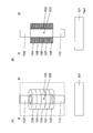
- FIG. 4B is a sectional view taken along the line X-X ′ in FIG. (A) is a bird's-eye view of a semiconductor device concerning the present invention.
- FIG. 4B is a sectional view taken along the line X-X ′ in FIG. (A) is a bird's-eye view of a semiconductor device concerning the present invention.
- FIG. 4B is a sectional view taken along the line X-X ′ in FIG. (A) is a bird's-eye view of a semiconductor device concerning the present invention.
- FIG. 4B is a sectional view taken along the line X-X ′ in FIG.
- the semiconductor layer of this embodiment is preferably a silicon layer.
- the semiconductor layer may be a group IV semiconductor such as Ge or C.
- the semiconductor layer may be a group III and group IV compound semiconductor.
- the first gate 104, the second gate 105, and the third gate 106 are electrically connected to each other.
- the first insulator 103 functions as a gate insulating film.
- the first insulator 103 includes at least one of an oxide film, a nitride film, an oxynitride film, and a high dielectric film, or at least one of an oxide film, a nitride film, an oxynitride film, and a high dielectric film. preferable.
- the second gate 105 is in contact with the first gate 104 and the third gate 106 is in contact with the second gate 105, the first gate 104 and the second gate are in contact with each other. 105 and the third gate 106 are electrically connected.
- the first gate 104, the second gate 105, the third gate 106, and the fourth gate 107 are electrically connected to each other.
- the first gate 104, the second gate 105, the third gate 106, the fourth gate 107, and the fifth gate 108 are electrically connected.
- the fourth gate 107 is in contact with the third gate 106 and the fifth gate 108 is in contact with the fourth gate 107, the third gate 106 and the fourth gate are in contact with each other. 107 and the fifth gate 108 are electrically connected.
- FIG. 2 shows a structure having sources or drains 109 and 110 on the top and bottom of the columnar semiconductor layer 102 in addition to FIG.
- the source or drain 109, 110 may be a diffusion layer.
- the second work function is preferably between 4.0 eV and 4.2 eV. Since the work function of n-type silicon is in the vicinity of 4.05 eV, the columnar semiconductor layer surrounded by the second gate 105 and the fourth gate 107 having the second work function is composed of silicon. At some point, it functions as n-type silicon.
- a compound of tantalum and titanium (TaTi) or tantalum nitride (TaN) is preferable.
- the first work function is preferably 4.2 eV or more.
- n is a transistor in which a channel is formed by gates having the first work function (the first gate 104, the third gate 106, and the fifth gate 108).
- a metal having a midgap work function, ruthenium (Ru), or titanium nitride (TiN) is preferable.
- the height of the first gate 104 and the third gate 106 is set to such a level that ballistic conduction occurs, two transistors having ballistic conduction are connected in series, thereby having ballistic conduction and a gate. Allows long transistors.
- the height of the first gate 104, the third gate 106, and the fifth gate 108 is high enough to cause ballistic conduction, two or more transistors having ballistic conduction are connected in series, so that Allows transistors with stick conduction and long gate length.
- the heights of the first gate 104, the third gate 106, and the fifth gate 108 are preferably the same.
- the second gate 105 and the fourth gate 107 are preferably the same height.
- the first work function is between 5.0 eV and 5.2 eV, it is in the vicinity of the work function of 5.15 eV of the p-type silicon, so that the first gate, the third gate and the fifth gate A portion of the columnar semiconductor layer 102 surrounded by p-type functions as p-type silicon.
- ruthenium (Ru) or titanium nitride (TiN) is preferable.
- a superlattice or a quantum well structure can be formed in the columnar semiconductor layer 102 by a work function difference between a metal and a semiconductor by a portion functioning as p-type silicon and a portion functioning as n-type silicon.
- the gates based on the first work function and the gate based on the second work function repeatedly surround the columnar semiconductor layer 102, whereby a superlattice can be formed in the columnar semiconductor layer 102.
- the second work function is preferably between 5.0 eV and 5.2 eV. Since the work function of p-type silicon is in the vicinity of 5.15 eV, the portion of the columnar semiconductor layer 102 surrounded by the second gate 105 and the fourth gate 107 having the second work function is When silicon, it functions as p-type silicon.
- ruthenium (Ru) or titanium nitride (TiN) is preferable.
- the first work function is preferably 5.0 eV or less.
- a transistor whose channel is formed by gates having the first work function (the first gate 104, the third gate 106, and the fifth gate 108) is p.
- a metal having a midgap work function, a compound of tantalum and titanium (TaTi), or tantalum nitride (TaN) is preferable.
- the first work function is between 4.0 eV and 4.2 eV, it is in the vicinity of the work function of 4.05 eV of n-type silicon, so the first gate, the third gate, and the fifth gate.
- the portion of the columnar semiconductor layer surrounded by n functions as n-type silicon.
- a compound of tantalum and titanium (TaTi) or tantalum nitride (TaN) is preferable.
- the second insulating film 211 formed between the first gate 104 and the second gate 105, the second gate 105, and the third gate.
- a third insulating film 212 formed between the first gate 106 and the third gate 106.
- a fourth insulating film 213 formed between the third gate 106 and the fourth gate 107 may be provided.
- a fifth insulating film 214 formed between the fourth gate 107 and the fifth gate 108 may be provided.
- the second insulating film 211, the third insulating film 212, the fourth insulating film 213, and the fifth insulating film 214 are either an oxide film, a nitride film, an oxynitride film, a high dielectric film, or an oxide film Preferably, at least one of a nitride film, an oxynitride film, and a high dielectric film is included.
- a semiconductor device in which p-type (including p + -type) and n-type (including n + -type) are opposite in conductivity type is naturally included in the technical scope of the present invention. It is.
Landscapes
- Insulated Gate Type Field-Effect Transistor (AREA)
- Thin Film Transistor (AREA)
- Electrodes Of Semiconductors (AREA)
Abstract
金属と半導体との仕事関数差によって柱状半導体層に超格子もしくは量子井戸構造を形成する構造を提供することを目的とする。基板上に形成された柱状半導体層と、前記柱状半導体層を囲む第1の絶縁物と、前記第1の絶縁物を取り囲む第1の仕事関数を有する金属からなる第1のゲートと、前記第1の絶縁物を取り囲む前記第1の仕事関数と異なる第2の仕事関数を有する金属からなる第2のゲートと、前記第2のゲートは前記第1のゲートの下方に位置するのであって、前記第1の絶縁物を取り囲む第1の仕事関数を有する金属からなる第3のゲートと、を有し、前記第3のゲートは前記第2のゲートの下方に位置するのであって、前記第1のゲートと前記第2のゲートと前記第3のゲートは電気的に接続することを特徴とすることにより上記課題を解決する。
Description
本発明は半導体装置に関する。
従来のSGTでは、ゲート長が短くなると、バリスティック伝導によりドレイン電流を向上させることができることが報告されている(例えば、特許文献1を参照)。バリスティック伝導とは、チャンネル長(ゲート長)がキャリアの平均自由工程より短くなると、キャリアが散乱を受けることなく、ソースからドレインまで走行するようになる現象を示す。
しかしながら、従来のSGTでは、シリコン柱径が5nmのとき、ゲート長10nm以下になると、サブスレッショルドスイングが増大することが報告されている(例えば、特許文献2を参照)。
一方で、Si/SiGe/Si/SiGe、Si/Ge/Si/Ge、又はn-Si/p-Si/n-Si交互層のような、種々の交互半導体層を含む基板をエッチングし、半導体ナノワイヤ中の埋め込み量子井戸又は超格子構造体を有する半導体ナノワイヤが報告されている(例えば、特許文献3を参照)。しかしながら、Si/SiGe/Si/SiGe、Si/Ge/Si/Geでは物質間に界面が存在し、欠陥の原因となる。また、n-Si/p-Si/n-Siでは、不純物の位置制御が難しい。また、不純物自体がキャリアの散乱の原因となる。
そこで、本発明は、金属と半導体との仕事関数差によって柱状半導体層に超格子もしくは量子井戸構造を形成する構造を提供することを目的とする。
本発明の半導体装置は、基板上に形成された柱状半導体層と、前記柱状半導体層を囲む第1の絶縁物と、前記第1の絶縁物を取り囲む第1の仕事関数を有する金属からなる第1のゲートと、前記第1の絶縁物を取り囲む前記第1の仕事関数と異なる第2の仕事関数を有する金属からなる第2のゲートと、前記第2のゲートは前記第1のゲートの下方に位置するのであって、前記第1の絶縁物を取り囲む第1の仕事関数を有する金属からなる第3のゲートと、を有し、前記第3のゲートは前記第2のゲートの下方に位置するのであって、前記第1のゲートと前記第2のゲートと前記第3のゲートは電気的に接続することを特徴とする。
また、前記第1の絶縁物を取り囲む前記第1の仕事関数と異なる第2の仕事関数を有する金属からなる第4のゲートと、を有し、前記第4のゲートは前記第3のゲートの下方に位置するのであって、前記第1のゲートと前記第2のゲートと前記第3のゲートと前記第4のゲートは電気的に接続することを特徴とする。
また、前記第1の絶縁物を取り囲む前記第1の仕事関数を有する金属からなる第5のゲートと、を有し、前記第5のゲートは前記第4のゲートの下方に位置するのであって、前記第1のゲートと前記第2のゲートと前記第3のゲートと前記第4のゲートと前記第5のゲートは電気的に接続することを特徴とする。
また、前記第2の仕事関数は、4.0eVから4.2eVの間であることを特徴とする。
また、前記第1の仕事関数は、4.2eV以上であることを特徴とする。
また、前記第2の仕事関数は、5.0eVから5.2eVの間であることを特徴とする。
また、前記第1の仕事関数は、5.0eV以下であることを特徴とする。
また、前記柱状半導体層の上部と下部にソースもしくはドレインを有することを特徴とする。
また、前記ソースもしくはドレインは拡散層からなることを特徴とする。
また、前記第1のゲートと前記第2のゲートとの間に形成された第2の絶縁膜と、前記第2のゲートと前記第3のゲートとの間に形成された第3の絶縁膜と、を有することを特徴とする。
また、前記第3のゲートと前記第4のゲートとの間に形成された第4の絶縁膜を有することを特徴とする。
また、前記第4のゲートと前記第5のゲートとの間に形成された第5の絶縁膜を有することを特徴とする。
本発明によれば、金属と半導体との仕事関数差によって柱状半導体層に超格子もしくは量子井戸構造を形成する構造を提供することができる。
基板上に形成された柱状半導体層と、前記柱状半導体層を囲む第1の絶縁物と、前記第1の絶縁物を取り囲む第1の仕事関数を有する金属からなる第1のゲートと、前記第1の絶縁物を取り囲む前記第1の仕事関数と異なる第2の仕事関数を有する金属からなる第2のゲートと、前記第2のゲートは前記第1のゲートの下方に位置するのであって、前記第1の絶縁物を取り囲む第1の仕事関数を有する金属からなる第3のゲートと、を有し、前記第3のゲートは前記第2のゲートの下方に位置するのであって、前記第1のゲートと前記第2のゲートと前記第3のゲートは電気的に接続することを特徴とすることにより、
例えば、柱状半導体層を柱状シリコン層とし、前記第1の仕事関数は、5.0eVから5.2eVの間とし、前記第2の仕事関数は、4.0eVから4.2eVの間とすると、p型シリコンの仕事関数5.15eVの近傍であるため、柱状半導体層の第1のゲートと第3のゲートに囲われた部分はp型シリコンとして機能し、n型シリコンの仕事関数4.05eVの近傍であるため、柱状半導体層の第2のゲートに囲われた部分はn型シリコンとして機能することにより、p型シリコンとして機能する部分とn型シリコンとして機能する部分とp型シリコンとして機能する部分とにより、金属と半導体との仕事関数差によって柱状半導体層に超格子もしくは量子井戸構造を形成することができる。
このとき、金属と半導体との仕事関数差によって柱状半導体層に超格子もしくは量子井戸構造を形成するから、p型シリコンとして機能する部分とn型シリコンとして機能する部分との間に界面は存在しないため、欠陥を減少させることができる。また、不純物を用いていないため、不純物の位置制御は不要であるし、不純物によるキャリアの散乱を抑制することができる。
例えば、柱状半導体層を柱状シリコン層とし、前記第1の仕事関数は、5.0eVから5.2eVの間とし、前記第2の仕事関数は、4.0eVから4.2eVの間とすると、p型シリコンの仕事関数5.15eVの近傍であるため、柱状半導体層の第1のゲートと第3のゲートに囲われた部分はp型シリコンとして機能し、n型シリコンの仕事関数4.05eVの近傍であるため、柱状半導体層の第2のゲートに囲われた部分はn型シリコンとして機能することにより、p型シリコンとして機能する部分とn型シリコンとして機能する部分とp型シリコンとして機能する部分とにより、金属と半導体との仕事関数差によって柱状半導体層に超格子もしくは量子井戸構造を形成することができる。
このとき、金属と半導体との仕事関数差によって柱状半導体層に超格子もしくは量子井戸構造を形成するから、p型シリコンとして機能する部分とn型シリコンとして機能する部分との間に界面は存在しないため、欠陥を減少させることができる。また、不純物を用いていないため、不純物の位置制御は不要であるし、不純物によるキャリアの散乱を抑制することができる。
また、前記第1の絶縁物を取り囲む前記第1の仕事関数と異なる第2の仕事関数を有する金属からなる第4のゲートと、前記第4のゲートは前記第3のゲートの下方に位置するのであって、前記第1のゲートと前記第2のゲートと前記第3のゲートと前記第4のゲートは電気的に接続することを特徴とし、前記第1の絶縁物を取り囲む前記第1の仕事関数を有する金属からなる第5のゲートと、を有し、前記第5のゲートは前記第4のゲートの下方に位置するのであって、前記第1のゲートと前記第2のゲートと前記第3のゲートと前記第4のゲートと前記第5のゲートは電気的に接続することを特徴とし、第1の仕事関数によるゲートと第2の仕事関数によるゲートが柱状半導体層を繰り返し取り囲むことにより、柱状半導体層内に超格子を形成することができる。
また、前記第1のゲートと前記第2のゲートとの間に形成された第2の絶縁膜と、前記第2のゲートと前記第3のゲートとの間に形成された第3の絶縁膜と、を有することを特徴とし、前記第3のゲートと前記第4のゲートとの間に形成された第4の絶縁膜を有することを特徴とし、前記第4のゲートと前記第5のゲートとの間に形成された第5の絶縁膜を有することを特徴とすることにより、各ゲートを絶縁膜により分離することで、第1の仕事関数を有する金属と第2の仕事関数を有する金属が混じることを抑制し、また、第1の仕事関数を有する金属と第2の仕事関数を有する金属により化合物が形成されることを抑制することができる。
また、基板上に形成された柱状半導体層と、前記柱状半導体層を囲む第1の絶縁物と、前記第1の絶縁物を取り囲む第1の仕事関数を有する金属からなる第1のゲートと、前記第1の絶縁物を取り囲む前記第1の仕事関数と異なる第2の仕事関数を有する金属からなる第2のゲートと、前記第2のゲートは前記第1のゲートの下方に位置するのであって、前記第1の絶縁物を取り囲む第1の仕事関数を有する金属からなる第3のゲートと、を有し、前記第3のゲートは前記第2のゲートの下方に位置するのであって、前記第1のゲートと前記第2のゲートと前記第3のゲートは電気的に接続することを特徴とし、前記柱状半導体層の上部と下部にソースもしくはドレインを有することを特徴とし、
例えば、柱状半導体層を柱状シリコン層とし、ソースもしくはドレインをn型とし、第1のゲートと第3のゲートの高さをバリスティック伝導が起こる程度の高さとし、前記第2の仕事関数は4.0eVから4.2eVの間とし、前記第1の仕事関数を前記第2の仕事関数以上の仕事関数とすると、柱状半導体層の第1のゲートと第3のゲートに囲われた部分はトランジスタのチャネルとして機能し、n型シリコンの仕事関数4.05eVの近傍であるため、柱状半導体層の第2のゲートに囲われた部分はn型シリコンとして機能することにより、チャネルとして機能する部分とn型シリコンとして機能する部分とチャネルとして機能する部分とにより、バリスティック伝導を有するトランジスタを2個直列することにより、バリスティック伝導を有し且つゲート長が長いトランジスタを可能とする。
例えば、柱状半導体層を柱状シリコン層とし、ソースもしくはドレインをn型とし、第1のゲートと第3のゲートの高さをバリスティック伝導が起こる程度の高さとし、前記第2の仕事関数は4.0eVから4.2eVの間とし、前記第1の仕事関数を前記第2の仕事関数以上の仕事関数とすると、柱状半導体層の第1のゲートと第3のゲートに囲われた部分はトランジスタのチャネルとして機能し、n型シリコンの仕事関数4.05eVの近傍であるため、柱状半導体層の第2のゲートに囲われた部分はn型シリコンとして機能することにより、チャネルとして機能する部分とn型シリコンとして機能する部分とチャネルとして機能する部分とにより、バリスティック伝導を有するトランジスタを2個直列することにより、バリスティック伝導を有し且つゲート長が長いトランジスタを可能とする。
また、前記第1の絶縁物を取り囲む前記第1の仕事関数と異なる第2の仕事関数を有する金属からなる第4のゲートと、前記第4のゲートは前記第3のゲートの下方に位置するのであって、前記第1のゲートと前記第2のゲートと前記第3のゲートと前記第4のゲートは電気的に接続することを特徴とし、前記第1の絶縁物を取り囲む前記第1の仕事関数を有する金属からなる第5のゲートと、を有し、前記第5のゲートは前記第4のゲートの下方に位置するのであって、前記第1のゲートと前記第2のゲートと前記第3のゲートと前記第4のゲートと前記第5のゲートは電気的に接続することを特徴とし、第1の仕事関数によるゲートと第2の仕事関数によるゲートが柱状半導体層を繰り返し取り囲むことにより、バリスティック伝導を有するトランジスタを2個以上直列することにより、バリスティック伝導を有し且つゲート長が長いトランジスタを可能とする。
以下、本発明の実施形態に係る、半導体装置を、図1、図2を参照しながら説明する。本実施例の半導体層は、シリコン層であることが好ましい。また、半導体層は、Ge、CといったIV族の半導体としてもよい。また、半導体層はIII族とIV族の化合物半導体としてもよい。
基板101上に形成された柱状半導体層102と、前記柱状半導体層102を囲む第1の絶縁物103と、前記第1の絶縁物103を取り囲む第1の仕事関数を有する金属からなる第1のゲート104と、前記第1の絶縁物103を取り囲む前記第1の仕事関数と異なる第2の仕事関数を有する金属からなる第2のゲート105と、前記第2のゲート105は前記第1のゲート104の下方に位置するのであって、前記第1の絶縁物103を取り囲む第1の仕事関数を有する金属からなる第3のゲート106と、を有し、前記第3のゲート106は前記第2のゲート105の下方に位置するのであって、前記第1のゲート104と前記第2のゲート105と前記第3のゲート106は電気的に接続することを特徴とする。
第1の絶縁物103はゲート絶縁膜として機能する。第1の絶縁物103は酸化膜、窒化膜、酸窒化膜、高誘電体膜のどれか、もしくは酸化膜、窒化膜、酸窒化膜、高誘電体膜のどれか一つを少なくとも含むことが好ましい。
第1のゲート104の下に第2のゲート105が接触し、第2のゲート105の下に第3のゲート106が接触していることで、前記第1のゲート104と前記第2のゲート105と前記第3のゲート106が電気的に接続している。
前記第1の絶縁物103を取り囲む前記第1の仕事関数と異なる第2の仕事関数を有する金属からなる第4のゲート107と、を有し、前記第4のゲート107は前記第3のゲート106の下方に位置するのであって、前記第1のゲート104と前記第2のゲート105と前記第3のゲート106と前記第4のゲート107は電気的に接続することを特徴とする。
前記第1の絶縁物103を取り囲む前記第1の仕事関数を有する金属からなる第5のゲート108と、を有し、前記第5のゲート108は前記第4のゲート107の下方に位置するのであって、前記第1のゲート104と前記第2のゲート105と前記第3のゲート106と前記第4のゲート107と前記第5のゲート108は電気的に接続することを特徴とする。
第3のゲート106の下に第4のゲート107が接触し、第4のゲート107の下に第5のゲート108が接触していることで、前記第3のゲート106と前記第4のゲート107と前記第5のゲート108が電気的に接続している。
図2には、図1に加えて、柱状半導体層102の上部と下部にソースもしくはドレイン109、110を有する構造が示される。柱状半導体層102の上部と下部にソースもしくはドレイン109、110を有することにより、トランジスタ動作を行うことができる。前記ソースもしくはドレイン109、110は拡散層としてもよい。
前記第2の仕事関数は、4.0eVから4.2eVの間であることが好ましい。n型シリコンの仕事関数4.05eVの近傍であるため、第2の仕事関数を有する第2のゲート105と第4のゲート107に囲まれた柱状半導体層の部分は、柱状半導体層がシリコンであるとき、n型シリコンとして機能する。例えば、タンタルとチタンの化合物(TaTi)や窒化タンタル(TaN)が好ましい。
また、前記第1の仕事関数は、4.2eV以上であることが好ましい。第1の仕事関数が4.2eV以上であると、第1の仕事関数を有するゲート(第1のゲート104、第3のゲート106、第5のゲート108)によりチャネルが形成されるトランジスタをn型のエンハンスメント型として動作することができる。例えば、ミッドギャップの仕事関数を持つ金属や、ルテニウム(Ru)や窒化チタン(TiN)が好ましい。
また、第1のゲート104と第3のゲート106の高さをバリスティック伝導が起こる程度の高さとすると、バリスティック伝導を有するトランジスタを2個直列することにより、バリスティック伝導を有し且つゲート長が長いトランジスタを可能とする。
また、第1のゲート104と第3のゲート106と第5のゲート108の高さをバリスティック伝導が起こる程度の高さとすると、バリスティック伝導を有するトランジスタを2個以上直列することにより、バリスティック伝導を有し且つゲート長が長いトランジスタを可能とする。
また、第1のゲート104と第3のゲート106と第5のゲート108の高さは同じであることが好ましい。また、第2のゲート105と第4のゲート107の高さは同じであることが好ましい。第1のゲート104と第3のゲート106と第5のゲート108の高さは同じであり、第2のゲート105と第4のゲート107の高さは同じであると、金属と半導体との仕事関数差によって柱状半導体層102に周期ポテンシャルを形成することができる。
また、第1の仕事関数が5.0eVから5.2eVの間であるとき、p型シリコンの仕事関数5.15eVの近傍であるため、第1のゲートと第3のゲートと第5のゲートに囲まれた柱状半導体層102の部分は、p型シリコンとして機能する。例えば、ルテニウム(Ru)や窒化チタン(TiN)が好ましい。
このとき、p型シリコンとして機能する部分とn型シリコンとして機能する部分とにより、金属と半導体との仕事関数差によって柱状半導体層102に超格子もしくは量子井戸構造を形成することができる。
上記のように、第1の仕事関数によるゲートと第2の仕事関数によるゲートが柱状半導体層102を繰り返し取り囲むことにより、柱状半導体層102内に超格子を形成することができる。
このとき、金属と半導体との仕事関数差によって柱状半導体層102に超格子もしくは量子井戸構造を形成するから、p型シリコンとして機能する部分とn型シリコンとして機能する部分との間に界面は存在しないため、欠陥を減少させることができる。また、不純物を用いていないため、不純物の位置制御は不要であるし、不純物によるキャリアの散乱を抑制することができる。
また、前記第2の仕事関数は、5.0eVから5.2eVの間であることが好ましい。p型シリコンの仕事関数5.15eVの近傍であるため、第2の仕事関数を有する第2のゲート105と第4のゲート107に囲まれた柱状半導体層102の部分は、柱状半導体層102がシリコンであるとき、p型シリコンとして機能する。例えば、ルテニウム(Ru)や窒化チタン(TiN)が好ましい。
また、前記第1の仕事関数は、5.0eV以下であることが好ましい。第1の仕事関数が5.0以下であると、第1の仕事関数を有するゲート(第1のゲート104、第3のゲート106、第5のゲート108)によりチャネルが形成されるトランジスタをp型のエンハンスメント型として動作することができる。例えば、ミッドギャップの仕事関数を持つ金属や、タンタルとチタンの化合物(TaTi)や窒化タンタル(TaN)が好ましい。
また、第1の仕事関数が4.0eVから4.2eVの間であるとき、n型シリコンの仕事関数4.05eVの近傍であるため、第1のゲートと第3のゲートと第5のゲートに囲まれた柱状半導体層の部分は、n型シリコンとして機能する。例えば、タンタルとチタンの化合物(TaTi)や窒化タンタル(TaN)が好ましい。
また、図3、図4に示すように、前記第1のゲート104と前記第2のゲート105との間に形成された第2の絶縁膜211と、前記第2のゲート105と前記第3のゲート106との間に形成された第3の絶縁膜212と、を有してもよい。
また、前記第3のゲート106と前記第4のゲート107との間に形成された第4の絶縁膜213を有してもよい。
また、前記第4のゲート107と前記第5のゲート108との間に形成された第5の絶縁膜214を有してもよい。
第2の絶縁膜211、第3の絶縁膜212、第4の絶縁膜213、第5の絶縁膜214は、酸化膜、窒化膜、酸窒化膜、高誘電体膜のどれか、もしくは酸化膜、窒化膜、酸窒化膜、高誘電体膜のどれか一つを少なくとも含むことが好ましい
各ゲート104、105、106、107、108を絶縁膜211、212、213、214により分離することで、第1の仕事関数を有する金属と第2の仕事関数を有する金属が混じることを抑制し、また、第1の仕事関数を有する金属と第2の仕事関数を有する金属により化合物が形成されることを抑制することができる。
このとき、各ゲート104、105、106、107、108をコンタクトや配線を用いて電気的に接続する必要がある。
なお、本発明は、本発明の広義の精神と範囲を逸脱することなく、様々な実施形態及び変形が可能とされるものである。また、上述した実施形態は、本発明の一実施例を説明するためのものであり、本発明の範囲を限定するものではない。
例えば、上記実施例において、p型(p+型を含む。)とn型(n+型を含む。)とをそれぞれ反対の導電型とした半導体装置も当然に本発明の技術的範囲に含まれる。
101.基板
102.柱状半導体層
103.第1の絶縁物
104.第1のゲート
105.第2のゲート
106.第3のゲート
107.第4のゲート
108.第5のゲート
109.ソースもしくはドレイン
110.ソースもしくはドレイン
211.第2の絶縁膜
212.第3の絶縁膜
213.第4の絶縁膜
214.第5の絶縁膜
102.柱状半導体層
103.第1の絶縁物
104.第1のゲート
105.第2のゲート
106.第3のゲート
107.第4のゲート
108.第5のゲート
109.ソースもしくはドレイン
110.ソースもしくはドレイン
211.第2の絶縁膜
212.第3の絶縁膜
213.第4の絶縁膜
214.第5の絶縁膜
Claims (12)
- 基板上に形成された柱状半導体層と、
前記柱状半導体層を囲む第1の絶縁物と、
前記第1の絶縁物を取り囲む第1の仕事関数を有する金属からなる第1のゲートと、
前記第1の絶縁物を取り囲む前記第1の仕事関数と異なる第2の仕事関数を有する金属からなる第2のゲートと、
前記第2のゲートは前記第1のゲートの下方に位置するのであって、
前記第1の絶縁物を取り囲む第1の仕事関数を有する金属からなる第3のゲートと、を有し、
前記第3のゲートは前記第2のゲートの下方に位置するのであって、
前記第1のゲートと前記第2のゲートと前記第3のゲートは電気的に接続することを特徴とする半導体装置。 - 前記第1の絶縁物を取り囲む前記第1の仕事関数と異なる第2の仕事関数を有する金属からなる第4のゲートと、を有し、
前記第4のゲートは前記第3のゲートの下方に位置するのであって、
前記第1のゲートと前記第2のゲートと前記第3のゲートと前記第4のゲートは電気的に接続することを特徴とする請求項1に記載の半導体装置。 - 前記第1の絶縁物を取り囲む前記第1の仕事関数を有する金属からなる第5のゲートと、を有し、
前記第5のゲートは前記第4のゲートの下方に位置するのであって、
前記第1のゲートと前記第2のゲートと前記第3のゲートと前記第4のゲートと前記第5のゲートは電気的に接続することを特徴とする請求項2に記載の半導体装置。 - 前記第2の仕事関数は、4.0eVから4.2eVの間であることを特徴とする請求項1~3に記載の半導体装置。
- 前記第1の仕事関数は、4.2eV以上であることを特徴とする請求項4に記載の半導体装置。
- 前記第2の仕事関数は、5.0eVから5.2eVの間であることを特徴とする請求項1~3に記載の半導体装置。
- 前記第1の仕事関数は、5.0eV以下であることを特徴とする請求項6に記載の半導体装置。
- 前記柱状半導体層の上部と下部にソースもしくはドレインを有することを特徴とする請求項1に記載の半導体装置。
- 前記ソースもしくはドレインは拡散層からなることを特徴とする請求項8に記載の半導体装置。
- 前記第1のゲートと前記第2のゲートとの間に形成された第2の絶縁膜と、
前記第2のゲートと前記第3のゲートとの間に形成された第3の絶縁膜と、
を有することを特徴とする請求項1に記載の半導体装置。 - 前記第3のゲートと前記第4のゲートとの間に形成された第4の絶縁膜を有することを特徴とする請求項2に記載の半導体装置。
- 前記第4のゲートと前記第5のゲートとの間に形成された第5の絶縁膜を有することを特徴とする請求項3に記載の半導体装置。
Priority Applications (3)
| Application Number | Priority Date | Filing Date | Title |
|---|---|---|---|
| PCT/JP2015/078821 WO2017061050A1 (ja) | 2015-10-09 | 2015-10-09 | 半導体装置 |
| JP2016563006A JP6339230B2 (ja) | 2015-10-09 | 2015-10-09 | 半導体装置 |
| US15/788,353 US10381451B2 (en) | 2015-10-09 | 2017-10-19 | Semiconductor device |
Applications Claiming Priority (1)
| Application Number | Priority Date | Filing Date | Title |
|---|---|---|---|
| PCT/JP2015/078821 WO2017061050A1 (ja) | 2015-10-09 | 2015-10-09 | 半導体装置 |
Related Child Applications (1)
| Application Number | Title | Priority Date | Filing Date |
|---|---|---|---|
| US15/788,353 Continuation US10381451B2 (en) | 2015-10-09 | 2017-10-19 | Semiconductor device |
Publications (1)
| Publication Number | Publication Date |
|---|---|
| WO2017061050A1 true WO2017061050A1 (ja) | 2017-04-13 |
Family
ID=58488314
Family Applications (1)
| Application Number | Title | Priority Date | Filing Date |
|---|---|---|---|
| PCT/JP2015/078821 Ceased WO2017061050A1 (ja) | 2015-10-09 | 2015-10-09 | 半導体装置 |
Country Status (3)
| Country | Link |
|---|---|
| US (1) | US10381451B2 (ja) |
| JP (1) | JP6339230B2 (ja) |
| WO (1) | WO2017061050A1 (ja) |
Cited By (4)
| Publication number | Priority date | Publication date | Assignee | Title |
|---|---|---|---|---|
| WO2019132883A1 (en) * | 2017-12-27 | 2019-07-04 | Intel Corporation | Vertical transistor-based logic gate |
| KR20210091289A (ko) * | 2018-12-21 | 2021-07-21 | 유니산티스 일렉트로닉스 싱가포르 프라이빗 리미티드 | 3 차원 반도체 장치의 제조 방법 |
| JP2024525817A (ja) * | 2021-07-13 | 2024-07-12 | ズィナイト コーポレイション | 薄膜半導体スイッチングデバイス |
| US12615804B1 (en) | 2024-10-31 | 2026-04-28 | Zinite Corporation | Thin-film transistors with metal oxide channel interfaces |
Families Citing this family (2)
| Publication number | Priority date | Publication date | Assignee | Title |
|---|---|---|---|---|
| WO2017085788A1 (ja) * | 2015-11-17 | 2017-05-26 | ユニサンティス エレクトロニクス シンガポール プライベート リミテッド | 半導体装置及び半導体装置の製造方法 |
| US11804532B2 (en) * | 2021-08-27 | 2023-10-31 | Taiwan Semiconductor Manufacturing Co., Ltd. | Gate-all-around devices with superlattice channel |
Citations (3)
| Publication number | Priority date | Publication date | Assignee | Title |
|---|---|---|---|---|
| JP2006310651A (ja) * | 2005-04-28 | 2006-11-09 | Toshiba Corp | 半導体装置の製造方法 |
| JP2008172164A (ja) * | 2007-01-15 | 2008-07-24 | Toshiba Corp | 半導体装置 |
| JP2013537709A (ja) * | 2010-07-21 | 2013-10-03 | キネテイツク・リミテツド | 半導体装置の製造方法 |
Family Cites Families (10)
| Publication number | Priority date | Publication date | Assignee | Title |
|---|---|---|---|---|
| JPH09298296A (ja) | 1996-04-23 | 1997-11-18 | Taiwan Moshii Denshi Kofun Yugenkoshi | 導電性側壁間隙を備えたmos電界効果トランジスタ及びその製造方法 |
| FR2830124B1 (fr) * | 2001-09-26 | 2005-03-04 | St Microelectronics Sa | Memoire vive |
| JP4108537B2 (ja) | 2003-05-28 | 2008-06-25 | 富士雄 舛岡 | 半導体装置 |
| KR100526889B1 (ko) * | 2004-02-10 | 2005-11-09 | 삼성전자주식회사 | 핀 트랜지스터 구조 |
| JP2006269520A (ja) * | 2005-03-22 | 2006-10-05 | Renesas Technology Corp | 半導体装置およびその製造方法 |
| KR100861236B1 (ko) * | 2007-04-10 | 2008-10-02 | 경북대학교 산학협력단 | 낮은 누설전류를 갖는 기둥형 전계효과트랜지스터 |
| JP2009200434A (ja) | 2008-02-25 | 2009-09-03 | Fujitsu Ltd | バリスティックmosトランジスタ |
| US8273591B2 (en) | 2008-03-25 | 2012-09-25 | International Business Machines Corporation | Super lattice/quantum well nanowires |
| US9997656B2 (en) * | 2014-12-17 | 2018-06-12 | Manjeri P. Anantram | Photodetector cell and solar panel with dual metal contacts and related methods |
| US9419003B1 (en) * | 2015-05-15 | 2016-08-16 | Taiwan Semiconductor Manufacturing Company, Ltd. | Semiconductor devices and methods of manufacture thereof |
-
2015
- 2015-10-09 JP JP2016563006A patent/JP6339230B2/ja not_active Expired - Fee Related
- 2015-10-09 WO PCT/JP2015/078821 patent/WO2017061050A1/ja not_active Ceased
-
2017
- 2017-10-19 US US15/788,353 patent/US10381451B2/en not_active Expired - Fee Related
Patent Citations (3)
| Publication number | Priority date | Publication date | Assignee | Title |
|---|---|---|---|---|
| JP2006310651A (ja) * | 2005-04-28 | 2006-11-09 | Toshiba Corp | 半導体装置の製造方法 |
| JP2008172164A (ja) * | 2007-01-15 | 2008-07-24 | Toshiba Corp | 半導体装置 |
| JP2013537709A (ja) * | 2010-07-21 | 2013-10-03 | キネテイツク・リミテツド | 半導体装置の製造方法 |
Cited By (6)
| Publication number | Priority date | Publication date | Assignee | Title |
|---|---|---|---|---|
| WO2019132883A1 (en) * | 2017-12-27 | 2019-07-04 | Intel Corporation | Vertical transistor-based logic gate |
| KR20210091289A (ko) * | 2018-12-21 | 2021-07-21 | 유니산티스 일렉트로닉스 싱가포르 프라이빗 리미티드 | 3 차원 반도체 장치의 제조 방법 |
| KR102535448B1 (ko) | 2018-12-21 | 2023-05-26 | 유니산티스 일렉트로닉스 싱가포르 프라이빗 리미티드 | 3 차원 반도체 장치의 제조 방법 |
| JP2024525817A (ja) * | 2021-07-13 | 2024-07-12 | ズィナイト コーポレイション | 薄膜半導体スイッチングデバイス |
| US12593467B2 (en) | 2021-07-13 | 2026-03-31 | Zinite Corporation | Thin film semiconductor switching device |
| US12615804B1 (en) | 2024-10-31 | 2026-04-28 | Zinite Corporation | Thin-film transistors with metal oxide channel interfaces |
Also Published As
| Publication number | Publication date |
|---|---|
| US20180047823A1 (en) | 2018-02-15 |
| US10381451B2 (en) | 2019-08-13 |
| JPWO2017061050A1 (ja) | 2017-10-05 |
| JP6339230B2 (ja) | 2018-06-06 |
Similar Documents
| Publication | Publication Date | Title |
|---|---|---|
| JP6339230B2 (ja) | 半導体装置 | |
| CN105322015B (zh) | 栅极结构及其制造方法 | |
| US20170025513A1 (en) | Semiconductor device | |
| US20170263768A1 (en) | Semiconductor device | |
| US20160149050A1 (en) | Reducing direct source-to-drain tunneling in field effect transistors with low effective mass channels | |
| CN107516668B (zh) | 半导体装置及其制造方法 | |
| US20160329400A1 (en) | Nanowire and method of fabricating the same | |
| JP6200103B2 (ja) | 半導体装置 | |
| JP5670605B2 (ja) | 半導体装置 | |
| JP6317507B2 (ja) | 半導体装置 | |
| JP5954597B2 (ja) | 半導体装置 | |
| JP6267369B2 (ja) | 半導体装置及び半導体装置の製造方法 | |
| JP5676807B1 (ja) | 半導体装置 | |
| JP6527839B2 (ja) | 半導体装置 | |
| JP6527835B2 (ja) | 半導体装置 | |
| JP6527831B2 (ja) | 半導体装置 | |
| JP5897676B2 (ja) | 半導体装置 | |
| JP5917672B2 (ja) | 半導体装置 | |
| JP5911948B2 (ja) | 半導体装置 | |
| JP5980288B2 (ja) | 半導体装置 | |
| JP6129387B2 (ja) | 半導体装置 | |
| JP6082489B2 (ja) | 半導体装置 | |
| JP6250210B2 (ja) | 半導体装置 | |
| JP2016072499A (ja) | 半導体装置 |
Legal Events
| Date | Code | Title | Description |
|---|---|---|---|
| ENP | Entry into the national phase |
Ref document number: 2016563006 Country of ref document: JP Kind code of ref document: A |
|
| 121 | Ep: the epo has been informed by wipo that ep was designated in this application |
Ref document number: 15905869 Country of ref document: EP Kind code of ref document: A1 |
|
| NENP | Non-entry into the national phase |
Ref country code: DE |
|
| 122 | Ep: pct application non-entry in european phase |
Ref document number: 15905869 Country of ref document: EP Kind code of ref document: A1 |