WO2017056877A1 - Abrasive diamond grain for wire tool and wire tool - Google Patents
Abrasive diamond grain for wire tool and wire tool Download PDFInfo
- Publication number
- WO2017056877A1 WO2017056877A1 PCT/JP2016/076188 JP2016076188W WO2017056877A1 WO 2017056877 A1 WO2017056877 A1 WO 2017056877A1 JP 2016076188 W JP2016076188 W JP 2016076188W WO 2017056877 A1 WO2017056877 A1 WO 2017056877A1
- Authority
- WO
- WIPO (PCT)
- Prior art keywords
- abrasive grains
- diamond
- palladium
- plating layer
- core wire
- Prior art date
Links
- 239000010432 diamond Substances 0.000 title claims abstract description 203
- 229910003460 diamond Inorganic materials 0.000 title claims abstract description 203
- KDLHZDBZIXYQEI-UHFFFAOYSA-N Palladium Chemical compound [Pd] KDLHZDBZIXYQEI-UHFFFAOYSA-N 0.000 claims abstract description 312
- 239000006061 abrasive grain Substances 0.000 claims abstract description 295
- 229910052763 palladium Inorganic materials 0.000 claims abstract description 157
- 238000000576 coating method Methods 0.000 claims abstract description 98
- 239000011248 coating agent Substances 0.000 claims abstract description 97
- 238000007747 plating Methods 0.000 claims description 208
- 239000002245 particle Substances 0.000 claims description 59
- 239000010410 layer Substances 0.000 description 101
- 238000005520 cutting process Methods 0.000 description 45
- 235000012431 wafers Nutrition 0.000 description 44
- PXHVJJICTQNCMI-UHFFFAOYSA-N Nickel Chemical compound [Ni] PXHVJJICTQNCMI-UHFFFAOYSA-N 0.000 description 36
- 238000000034 method Methods 0.000 description 31
- 238000011156 evaluation Methods 0.000 description 27
- 229910052751 metal Inorganic materials 0.000 description 26
- 239000002184 metal Substances 0.000 description 26
- 230000008569 process Effects 0.000 description 23
- 229910052759 nickel Inorganic materials 0.000 description 18
- 238000012545 processing Methods 0.000 description 15
- 238000011282 treatment Methods 0.000 description 14
- 239000012190 activator Substances 0.000 description 12
- 239000010408 film Substances 0.000 description 10
- 239000000463 material Substances 0.000 description 10
- 230000002093 peripheral effect Effects 0.000 description 7
- RTAQQCXQSZGOHL-UHFFFAOYSA-N Titanium Chemical compound [Ti] RTAQQCXQSZGOHL-UHFFFAOYSA-N 0.000 description 6
- 150000002941 palladium compounds Chemical class 0.000 description 6
- 238000004519 manufacturing process Methods 0.000 description 5
- KERTUBUCQCSNJU-UHFFFAOYSA-L nickel(2+);disulfamate Chemical compound [Ni+2].NS([O-])(=O)=O.NS([O-])(=O)=O KERTUBUCQCSNJU-UHFFFAOYSA-L 0.000 description 5
- 238000005238 degreasing Methods 0.000 description 4
- 238000010586 diagram Methods 0.000 description 4
- 229910052594 sapphire Inorganic materials 0.000 description 4
- 239000010980 sapphire Substances 0.000 description 4
- 230000003746 surface roughness Effects 0.000 description 4
- 239000010936 titanium Substances 0.000 description 4
- 229910052719 titanium Inorganic materials 0.000 description 4
- RYGMFSIKBFXOCR-UHFFFAOYSA-N Copper Chemical compound [Cu] RYGMFSIKBFXOCR-UHFFFAOYSA-N 0.000 description 3
- HEMHJVSKTPXQMS-UHFFFAOYSA-M Sodium hydroxide Chemical compound [OH-].[Na+] HEMHJVSKTPXQMS-UHFFFAOYSA-M 0.000 description 3
- 239000000853 adhesive Substances 0.000 description 3
- 230000001070 adhesive effect Effects 0.000 description 3
- 230000008859 change Effects 0.000 description 3
- 229910052802 copper Inorganic materials 0.000 description 3
- 239000010949 copper Substances 0.000 description 3
- 230000000694 effects Effects 0.000 description 3
- 230000005684 electric field Effects 0.000 description 3
- 239000007788 liquid Substances 0.000 description 3
- 238000006722 reduction reaction Methods 0.000 description 3
- 229910052710 silicon Inorganic materials 0.000 description 3
- 239000010703 silicon Substances 0.000 description 3
- 238000005406 washing Methods 0.000 description 3
- 229910021586 Nickel(II) chloride Inorganic materials 0.000 description 2
- 229910045601 alloy Inorganic materials 0.000 description 2
- 239000000956 alloy Substances 0.000 description 2
- PNEYBMLMFCGWSK-UHFFFAOYSA-N aluminium oxide Inorganic materials [O-2].[O-2].[O-2].[Al+3].[Al+3] PNEYBMLMFCGWSK-UHFFFAOYSA-N 0.000 description 2
- -1 amine salt compound Chemical class 0.000 description 2
- KGBXLFKZBHKPEV-UHFFFAOYSA-N boric acid Chemical compound OB(O)O KGBXLFKZBHKPEV-UHFFFAOYSA-N 0.000 description 2
- 239000004327 boric acid Substances 0.000 description 2
- 239000003093 cationic surfactant Substances 0.000 description 2
- 239000011247 coating layer Substances 0.000 description 2
- 230000000052 comparative effect Effects 0.000 description 2
- 230000007423 decrease Effects 0.000 description 2
- 238000009826 distribution Methods 0.000 description 2
- 239000000835 fiber Substances 0.000 description 2
- 239000011521 glass Substances 0.000 description 2
- 239000003365 glass fiber Substances 0.000 description 2
- 230000006872 improvement Effects 0.000 description 2
- 238000012986 modification Methods 0.000 description 2
- 230000004048 modification Effects 0.000 description 2
- QMMRZOWCJAIUJA-UHFFFAOYSA-L nickel dichloride Chemical compound Cl[Ni]Cl QMMRZOWCJAIUJA-UHFFFAOYSA-L 0.000 description 2
- 239000010453 quartz Substances 0.000 description 2
- 230000036632 reaction speed Effects 0.000 description 2
- VYPSYNLAJGMNEJ-UHFFFAOYSA-N silicon dioxide Inorganic materials O=[Si]=O VYPSYNLAJGMNEJ-UHFFFAOYSA-N 0.000 description 2
- 239000000126 substance Substances 0.000 description 2
- 239000010409 thin film Substances 0.000 description 2
- 239000002699 waste material Substances 0.000 description 2
- XLYOFNOQVPJJNP-UHFFFAOYSA-N water Substances O XLYOFNOQVPJJNP-UHFFFAOYSA-N 0.000 description 2
- 238000004804 winding Methods 0.000 description 2
- 238000012935 Averaging Methods 0.000 description 1
- ZOXJGFHDIHLPTG-UHFFFAOYSA-N Boron Chemical compound [B] ZOXJGFHDIHLPTG-UHFFFAOYSA-N 0.000 description 1
- 229910001369 Brass Inorganic materials 0.000 description 1
- 229920000049 Carbon (fiber) Polymers 0.000 description 1
- ZOKXTWBITQBERF-UHFFFAOYSA-N Molybdenum Chemical compound [Mo] ZOKXTWBITQBERF-UHFFFAOYSA-N 0.000 description 1
- 229910000831 Steel Inorganic materials 0.000 description 1
- QAOWNCQODCNURD-UHFFFAOYSA-L Sulfate Chemical compound [O-]S([O-])(=O)=O QAOWNCQODCNURD-UHFFFAOYSA-L 0.000 description 1
- 238000010521 absorption reaction Methods 0.000 description 1
- 238000004220 aggregation Methods 0.000 description 1
- 230000002776 aggregation Effects 0.000 description 1
- 229920006231 aramid fiber Polymers 0.000 description 1
- 230000015572 biosynthetic process Effects 0.000 description 1
- 229910052796 boron Inorganic materials 0.000 description 1
- 239000010951 brass Substances 0.000 description 1
- 239000004917 carbon fiber Substances 0.000 description 1
- 125000002091 cationic group Chemical group 0.000 description 1
- 239000000919 ceramic Substances 0.000 description 1
- 238000006243 chemical reaction Methods 0.000 description 1
- 239000003795 chemical substances by application Substances 0.000 description 1
- 150000001875 compounds Chemical class 0.000 description 1
- 239000012141 concentrate Substances 0.000 description 1
- 229920001940 conductive polymer Polymers 0.000 description 1
- 239000004020 conductor Substances 0.000 description 1
- PYRZPBDTPRQYKG-UHFFFAOYSA-N cyclopentene-1-carboxylic acid Chemical compound OC(=O)C1=CCCC1 PYRZPBDTPRQYKG-UHFFFAOYSA-N 0.000 description 1
- 230000008021 deposition Effects 0.000 description 1
- 230000006866 deterioration Effects 0.000 description 1
- 238000007772 electroless plating Methods 0.000 description 1
- 238000009713 electroplating Methods 0.000 description 1
- 238000000921 elemental analysis Methods 0.000 description 1
- 230000007613 environmental effect Effects 0.000 description 1
- 239000012530 fluid Substances 0.000 description 1
- 238000010191 image analysis Methods 0.000 description 1
- 238000003754 machining Methods 0.000 description 1
- 230000014759 maintenance of location Effects 0.000 description 1
- 238000013507 mapping Methods 0.000 description 1
- 238000005259 measurement Methods 0.000 description 1
- 238000000691 measurement method Methods 0.000 description 1
- 239000002923 metal particle Substances 0.000 description 1
- VNWKTOKETHGBQD-UHFFFAOYSA-N methane Chemical compound C VNWKTOKETHGBQD-UHFFFAOYSA-N 0.000 description 1
- 229910000510 noble metal Inorganic materials 0.000 description 1
- 239000003921 oil Substances 0.000 description 1
- HBEQXAKJSGXAIQ-UHFFFAOYSA-N oxopalladium Chemical compound [Pd]=O HBEQXAKJSGXAIQ-UHFFFAOYSA-N 0.000 description 1
- 150000002940 palladium Chemical class 0.000 description 1
- 229910003445 palladium oxide Inorganic materials 0.000 description 1
- PIBWKRNGBLPSSY-UHFFFAOYSA-L palladium(II) chloride Chemical compound Cl[Pd]Cl PIBWKRNGBLPSSY-UHFFFAOYSA-L 0.000 description 1
- YJVFFLUZDVXJQI-UHFFFAOYSA-L palladium(ii) acetate Chemical compound [Pd+2].CC([O-])=O.CC([O-])=O YJVFFLUZDVXJQI-UHFFFAOYSA-L 0.000 description 1
- GPNDARIEYHPYAY-UHFFFAOYSA-N palladium(ii) nitrate Chemical compound [Pd+2].[O-][N+]([O-])=O.[O-][N+]([O-])=O GPNDARIEYHPYAY-UHFFFAOYSA-N 0.000 description 1
- 229920000642 polymer Polymers 0.000 description 1
- 229920005594 polymer fiber Polymers 0.000 description 1
- 230000009467 reduction Effects 0.000 description 1
- 238000011946 reduction process Methods 0.000 description 1
- 239000011347 resin Substances 0.000 description 1
- 229920005989 resin Polymers 0.000 description 1
- 238000007788 roughening Methods 0.000 description 1
- 239000013535 sea water Substances 0.000 description 1
- 238000010008 shearing Methods 0.000 description 1
- 238000009751 slip forming Methods 0.000 description 1
- 239000002002 slurry Substances 0.000 description 1
- 229910001220 stainless steel Inorganic materials 0.000 description 1
- 239000010959 steel Substances 0.000 description 1
- 238000012360 testing method Methods 0.000 description 1
- WFKWXMTUELFFGS-UHFFFAOYSA-N tungsten Chemical compound [W] WFKWXMTUELFFGS-UHFFFAOYSA-N 0.000 description 1
Images


Classifications
-
- B—PERFORMING OPERATIONS; TRANSPORTING
- B23—MACHINE TOOLS; METAL-WORKING NOT OTHERWISE PROVIDED FOR
- B23D—PLANING; SLOTTING; SHEARING; BROACHING; SAWING; FILING; SCRAPING; LIKE OPERATIONS FOR WORKING METAL BY REMOVING MATERIAL, NOT OTHERWISE PROVIDED FOR
- B23D61/00—Tools for sawing machines or sawing devices; Clamping devices for these tools
- B23D61/18—Sawing tools of special type, e.g. wire saw strands, saw blades or saw wire equipped with diamonds or other abrasive particles in selected individual positions
-
- B—PERFORMING OPERATIONS; TRANSPORTING
- B28—WORKING CEMENT, CLAY, OR STONE
- B28D—WORKING STONE OR STONE-LIKE MATERIALS
- B28D5/00—Fine working of gems, jewels, crystals, e.g. of semiconductor material; apparatus or devices therefor
- B28D5/0058—Accessories specially adapted for use with machines for fine working of gems, jewels, crystals, e.g. of semiconductor material
- B28D5/007—Use, recovery or regeneration of abrasive mediums
-
- B—PERFORMING OPERATIONS; TRANSPORTING
- B24—GRINDING; POLISHING
- B24B—MACHINES, DEVICES, OR PROCESSES FOR GRINDING OR POLISHING; DRESSING OR CONDITIONING OF ABRADING SURFACES; FEEDING OF GRINDING, POLISHING, OR LAPPING AGENTS
- B24B27/00—Other grinding machines or devices
- B24B27/06—Grinders for cutting-off
- B24B27/0633—Grinders for cutting-off using a cutting wire
-
- B—PERFORMING OPERATIONS; TRANSPORTING
- B24—GRINDING; POLISHING
- B24D—TOOLS FOR GRINDING, BUFFING OR SHARPENING
- B24D11/00—Constructional features of flexible abrasive materials; Special features in the manufacture of such materials
-
- B—PERFORMING OPERATIONS; TRANSPORTING
- B24—GRINDING; POLISHING
- B24D—TOOLS FOR GRINDING, BUFFING OR SHARPENING
- B24D3/00—Physical features of abrasive bodies, or sheets, e.g. abrasive surfaces of special nature; Abrasive bodies or sheets characterised by their constituents
-
- B—PERFORMING OPERATIONS; TRANSPORTING
- B24—GRINDING; POLISHING
- B24D—TOOLS FOR GRINDING, BUFFING OR SHARPENING
- B24D3/00—Physical features of abrasive bodies, or sheets, e.g. abrasive surfaces of special nature; Abrasive bodies or sheets characterised by their constituents
- B24D3/02—Physical features of abrasive bodies, or sheets, e.g. abrasive surfaces of special nature; Abrasive bodies or sheets characterised by their constituents the constituent being used as bonding agent
- B24D3/04—Physical features of abrasive bodies, or sheets, e.g. abrasive surfaces of special nature; Abrasive bodies or sheets characterised by their constituents the constituent being used as bonding agent and being essentially inorganic
- B24D3/06—Physical features of abrasive bodies, or sheets, e.g. abrasive surfaces of special nature; Abrasive bodies or sheets characterised by their constituents the constituent being used as bonding agent and being essentially inorganic metallic or mixture of metals with ceramic materials, e.g. hard metals, "cermets", cements
-
- B—PERFORMING OPERATIONS; TRANSPORTING
- B28—WORKING CEMENT, CLAY, OR STONE
- B28D—WORKING STONE OR STONE-LIKE MATERIALS
- B28D5/00—Fine working of gems, jewels, crystals, e.g. of semiconductor material; apparatus or devices therefor
- B28D5/04—Fine working of gems, jewels, crystals, e.g. of semiconductor material; apparatus or devices therefor by tools other than rotary type, e.g. reciprocating tools
- B28D5/045—Fine working of gems, jewels, crystals, e.g. of semiconductor material; apparatus or devices therefor by tools other than rotary type, e.g. reciprocating tools by cutting with wires or closed-loop blades
Definitions
- the present invention relates to a diamond abrasive for a wire tool and a wire tool, which can cut a hard and brittle material such as silicon or sapphire, and has a surface coated with palladium in an optimum state.
- wire tools have been used to cut hard and brittle materials such as glass, ceramic, quartz, sapphire, and silicon.
- a method of slicing an object to be processed while supplying a slurry containing abrasive grains using a steel wire so-called free abrasive grain machining.
- a grinding waste liquid containing a large amount of abrasive grains and workpiece cutting waste is generated. Therefore, there is a problem that this processing is necessary and the environmental load is large.
- conductive particles are dispersed in the form of dots on the surface of the diamond abrasive grains, and the diamond abrasive grains are fixed by plating with a part of the diamond abrasive grains exposed.
- a tool is used (Patent Document 3).
- a high strength and conductive core wire, diamond abrasive grains provided on the outer periphery of the core wire, and a plating layer formed on the outer periphery of the core wire and holding the diamond abrasive grains are provided on the surface of the diamond abrasive grains. Is dotted with metal nuclei, and the thickness of the plating layer at the tip of the diamond abrasive grain is thinner than the thickness of the plating layer on the surface of the core wire at a part other than the diamond abrasive grain, in the radial direction of the core wire.
- Patent Document 4 There is a wire tool characterized by (Patent Document 4).
- the electric field is also concentrated on the convex portion when performing a plating process for fixing the diamond.
- the plating layer on the abrasive grain of diamond becomes thicker than the plating layer on a core wire.
- the plating layer on the diamond abrasive grains becomes thick, it takes time to expose the blade edges of the diamond abrasive grains that contribute to processing, and thus the sharpness at the initial stage of cutting is poor, causing thickness variations of each wafer and warping of the wafers.
- Patent Document 3 since the abrasive grains are only buried in the plating layer, the adhesive strength of the abrasive grains is not sufficient, and there is a problem that the diamond abrasive grains fall off. When the abrasive grains fall off, the diameter of the wire tool changes, the wafer thickness varies, and warping may occur.
- Patent Document 4 shows that current flows preferentially only in the portion where the metal core on the abrasive grain surface is covered in a dot-like manner, and overall, it is difficult for current to flow when energized.
- the variation of the current that is energized increases, and as a result, the coating thickness of the plating layer formed on the surface of the metal core tends to vary.
- Patent Document 4 the metal core is coated in an island shape, the adhesive force of the abrasive grains to the core wire is not sufficient, and the abrasive grains are likely to fall off. Therefore, there is a problem that the cutting accuracy during use is greatly deteriorated over time.
- the present invention has been made in view of such a problem, and it is a diamond for a wire tool that can reliably hold diamond abrasive grains and suppress the thickness variation, warpage, and scratches of a wafer to be cut.
- An object is to provide an abrasive and a wire tool.
- the first invention is a diamond abrasive grain in which a part of the surface of the diamond particle is coated with palladium, and the surface of the diamond particle is coated with palladium from 0.01 ⁇ m to 0.
- a sea part that is substantially continuously coated with a thickness of 5 ⁇ m, and an exposed part where the surface of the diamond particle is exposed without being covered with palladium, and the area ratio of the sea part is the diamond particle
- the diamond abrasive for wire tools is characterized in that the surface area is 70% or more and 90% or less, and the remaining part is the exposed part.
- palladium may be partially scattered in the island-like part where the surface of the abrasive grains is exposed without being covered with palladium.
- the sea part is a part where the whole is connected to each other on the surface.
- an island part island-like part
- the sea part in which palladium is substantially continuously coated means that the surface of the diamond particle is formed so that palladium is continuously connected to the whole. That is, in the present invention, palladium at any part is connected in a sea state, and all palladium at any part on the diamond particle is electrically connected.
- the exposed portions of the diamond particles that are not covered with palladium on the surface of the diamond abrasive grains and that are scattered in an island shape are not covered with palladium, and the portions where the surfaces of the diamond particles are exposed to each other It is formed independently. That is, the exposed portions of the individual island-like diamond particles are formed apart from each other. Note that some metal nuclei may be scattered in the exposed portions of the island-shaped diamond particles.
- the average particle diameter of diamond to be used can be appropriately selected depending on the type of hard and brittle material to be cut. Specifically, the average particle diameter of diamond is desirably 5 to 70 ⁇ m, and more desirably 10 to 60 ⁇ m.
- the first invention since most of the surface of the diamond abrasive grains is covered with palladium in a thin sea shape, it is possible to energize the entire diamond abrasive grain surface during the plating process. Can be fixed with a sufficient holding force.
- a part of the surface of the diamond abrasive grain is not covered with palladium, and a large number of exposed portions where the surface of the diamond particle is exposed in an island shape are formed. For this reason, compared with the case where the whole surface of an abrasive grain is coat
- the initial sharpness of the wire tool is good, and the cutting ability of the wire tool can be exhibited immediately after the start of cutting. As a result, the quality of the wafer after cutting is improved.
- the plating layer is not formed on the diamond abrasive grains so as to cover the entire abrasive grains, so that other diamond abrasive grains are not attracted and aggregation of the abrasive grains occurs. do not do. For this reason, the wire tool has a constant outer diameter, and the quality of the wafer after cutting is improved.
- the adhesion between palladium and plating is high and firmly fixed, it is possible to suppress the diamond abrasive grains from falling off during processing.
- Nickel and titanium form a passive film on the surface, so the adhesion to the diamond abrasive grains is weak, but palladium does not passivate. It is possible to prevent the abrasive grains from dropping off.
- 2nd invention comprises the diamond abrasive grain concerning 1st invention, the core wire which has electroconductivity, and the plating layer which is formed in the outer periphery of the said core wire, and hold
- the said plating layer is An average of the abrasive plating layer on the surface of the diamond abrasive grains in a portion protruding from the core wire plating layer, comprising a core plating layer covering the surface of the core wire and an abrasive plating layer covering the surface of the diamond abrasive grains
- the wire tool is characterized in that the thickness is 0.2 or more and 0.8 or less with respect to the average thickness of the core wire plating layer.
- maintaining the said diamond abrasive grain are comprised,
- the said plating layer is the surface of the said core wire A part of the abrasive plating layer at the tip of the diamond abrasive grains is removed, and at least a part of the diamond abrasive grains A part of the tip of the wire tool is exposed.
- the diamond abrasive grains used for the wire tool are abrasive grains having different diameters depending on the intended use. For this reason, it is necessary to maintain the holding power of the abrasive grains and the surface quality of the work material after cutting with respect to the diamond abrasive grains of different sizes. There are constraints. For example, it is desirable that the average thickness of the core wire plating layer is not less than 0.25 times and not more than 0.75 times the average particle diameter of the diamond abrasive grains.
- the thickness of the core plating layer forms a base portion of the plating layer in which the lower part of the diamond abrasive grains is embedded to a predetermined depth in the portion where the diamond abrasive grains are fixed. Further, a plating layer is formed on the surface of the diamond abrasive grains in a state continuous from the base portion, and the abrasive grains are held in this state. Therefore, the average thickness of the core wire plating layer is a base of the fixing force of the diamond abrasive grains. In order to obtain a stable fixing force against the shear stress acting on the diamond abrasive grains during cutting, the diamond abrasive A core wire plating thickness of 0.25 times or more of the average grain size of the grains is required.
- the diamond abrasive grains easily fall off.
- the thickness E of the base portion is 0.75 times or more, the protruding amount of the abrasive grains becomes small and slipping easily occurs, and the sharpness decreases because the protruding amount of the abrasive grains becomes smaller as the processing proceeds.
- a strike plating layer may be provided on the surface of the core wire.
- the strike plating layer may be formed of nickel or an alloy thereof. By having the strike plating layer, the diamond abrasive grains easily adhere to the core wire.
- the effect of diamond abrasive grains is remarkable when the coverage of palladium is 70 to 90%.
- the ratio of the average thickness of the abrasive plating layer formed on the surface of the diamond abrasive grains in the portion protruding from the core wire plating layer, which is the plating layer on the core wire surface, to the average thickness of the core wire plating layer is 0.2 or more and 0.
- the cutting ability of the wire tool can be exhibited immediately after the start of cutting.
- the dressing time with the grindstone is short, and it is not necessary to apply the dressing strongly. For this reason, it is possible to prevent the diamond abrasive grains from falling off and lowering the fixing force in the dressing process, and the productivity is improved.
- the average thickness of the core wire plating layer is set to 0.25 times or more of the average particle diameter of the diamond abrasive grains to ensure the holding power of the diamond abrasive grains, and to 0.75 times or less, the diamond in the wire tool The cutting quality of the abrasive grains can be ensured.
- the current flowing on the surface of the core wire is stable when electrodepositing the diamond abrasive grains, and the diamond abrasive grains can be stably attached.
- the adhesion of the plating layer can be improved by the anchor effect.
- a diamond abrasive for a wire tool and a wire tool that can reliably hold the diamond abrasive and suppress the variation in thickness of the wafer to be cut and the occurrence of scratches.
- FIG. Sectional drawing of the wire tool 7.
- FIG. The expanded sectional view of the abrasive grain 13.
- FIG. The figure which shows the diamond particle.
- FIG. Schematic shows the wire tool manufacturing apparatus 20.
- FIG. The figure which shows the measuring method of TTV (TV5).
- FIG. 1 is a schematic view showing a cutting device 1.
- the cutting device 1 is for slicing an ingot 3 that is an object to be cut.
- the cutting device 1 includes a holding unit 5 that holds the ingot 3, a roller 9 having a multi-groove for moving the wire tool 7, a motor (not shown) for driving the holding unit 5 and the roller 9, and the like. Composed.
- the wire tool 7 is wound around the outer circumference of the roller 9 many times in a state where a predetermined tension is applied.
- the wire tool 7 is fed from one side (in the direction of arrow A in the figure) and wound up from the other side (in the direction of arrow B in the figure).
- the wire tool 7 can be reciprocated between the rollers 9 by reversibly rotating the rollers 9 by the drive motor.
- the ingot 3 which is a hard and brittle material such as silicon or sapphire is held by the holding portion 5, it is moved perpendicularly to the moving direction of the wire tool 7 (in the direction of arrow C in the figure).
- the wire tool 7 cuts the ingot 3 by applying a predetermined load to the holding unit 5 and bringing the ingot 3 into contact with the wire tool 7. That is, the ingot 3 can be sliced into a large number of workpieces at a time.
- the cutting method of the present invention is not limited to the illustrated example, and can be applied to all cutting processes performed using the wire tool according to the present invention.
- FIG. 2 is a view showing a cross section of the wire tool 7 in a direction perpendicular to the axial direction.
- the wire tool 7 is mainly composed of a core wire 11, abrasive grains 13, a plating layer 15, and the like.
- the core wire 11 is a metal wire having high strength and conductivity.
- a piano wire, a stainless steel wire, a tungsten wire, a molybdenum wire, or the like can be used.
- a non-metallic wire such as glass fiber, aramid fiber, carbon fiber, alumina fiber, boron fiber, etc., on which a conductive coating layer is formed can be applied.
- strike plating can be formed on the surface of the core wire 11.
- the metal used for the strike plating layer can be selected from nickel, copper, brass, and the like that are compatible with the later nickel plating.
- Strike plating has a role as a base plating and has an effect of electrodepositing diamond abrasive grains stably and uniformly.
- the surface conductive layer of the core wire is formed by performing metal plating on the glass fiber or polymer fiber by electroless plating. Can be formed.
- a conductive polymer can be used on the outer peripheral surface of the core wire, or a conductive material such as Ag can be contained and dispersed in the polymer to impart conductivity.
- the outer diameter of the core wire 11 is preferably 80 ⁇ m to 300 ⁇ m. If the outer diameter of the core wire 11 is too small, the tensile strength of the core wire 11 is reduced, and there is a risk of breakage during use. On the other hand, if the outer diameter of the core wire 11 is too large, the cutting allowance (curfloss) increases, and the yield during cutting decreases.
- Abrasive grains 13 are fixed to the outer periphery of the core wire 11.
- the abrasive grains 13 are diamond abrasive grains. That is, the abrasive grains 13 are diamond abrasive grains for wire tools.
- the average particle size of the abrasive grains 13 is preferably 5 ⁇ m to 70 ⁇ m, and more preferably 10 to 60 ⁇ m. When the particle size of the abrasive grains 13 is too small, the cutting ability is inferior.
- the grain size of the abrasive grains 13 is too large, it is necessary to increase the thickness of the abrasive grain holding layer for holding the abrasive grains 13, so that the outer diameter of the wire tool 7 is increased and the yield is reduced. .
- the average particle size of the abrasive grains 13 in the present invention is the average particle size (arithmetic average particle size) of distribution measured by a general laser diffraction particle size distribution measuring device (for example, SALD-2300 manufactured by Shimadzu Corporation). To do. Details of the surface properties of the abrasive grains 13 will be described later.
- the plating layer 15 is formed on the outer periphery of the core wire 11 and functions as a holding layer for the abrasive grains 13.
- the plating layer 15 may be any metal as long as it can hold the abrasive grains 13, but plating made of nickel or an alloy thereof is most preferable.
- the thickness of the plating layer 15 is set according to the average particle diameter of the abrasive grains 13.
- the plating layer 15 is composed of a core wire plating layer covering the surface of the core wire 11 and an abrasive plating layer covering the surface of the abrasive grain 13.
- FIG. 3 is an enlarged cross-sectional view of the abrasive grain 13.
- the average thickness E of the base part (core wire plating layer 15a) of the plating layer 15 on the surface of the core wire 11 in a portion other than the abrasive grains 13 is 0.25 times or more and 0.75 times or less the average particle diameter of the abrasive grains 13. Is preferred.
- the average thickness of the core wire plating layer 15 a forms the base portion of the plating layer in which the lower part of the diamond abrasive grains is embedded to a predetermined depth when the diamond abrasive grains are fixed, but the thickness E of the core wire plating layer 15 a is that of the abrasive grains 13.
- the abrasive grains 13 cannot be sufficiently held, and the abrasive grains 13 may fall off due to the shearing force during processing. Further, if the thickness E of the core wire plating layer 15a is larger than 0.75 times the average particle diameter of the abrasive grains 13, the abrasive grains 13 can be held firmly, but slipping easily occurs at the initial stage of processing, and if the processing proceeds. As it progresses, the protruding amount of the abrasive grains 13 becomes smaller, the sharpness is lowered, and the wafer may be warped.
- the plating layer 15 (abrasive) formed on the surface of the abrasive grains 13 in the portion protruding from the plating layer 15 (core wire plating layer 15a) on the surface of the core wire 11
- the ratio of the thickness D of the grain plating layer 15b) is preferably 0.2 or more and 0.8 or less.
- the dressing takes time. Further, when the thickness D of the abrasive plating layer 15b is smaller than 0.2 times the thickness E of the core plating layer 15a, the plating layer 15 on the abrasive grain 13 becomes too thin and the abrasive grains 13 are sufficiently fixed. There is a risk of disappearing.
- tip part of the abrasive grain 13 is removed, and at least one part (preferably 90% or more of the abrasive grain 13) is removed. It is desirable to expose a part of the tip of the abrasive grains 13. By doing in this way, the cutting ability of a wire tool can be exhibited from the initial stage of use.
- the exposed state of the tip of the abrasive grain 13 is confirmed by observing a predetermined region with an electron microscope (SEM) + elemental analysis and counting the number of the regions.
- FIG. 4A to 4C are conceptual diagrams of the abrasive grains 13
- FIG. 4A is a diagram showing the diamond particles 14 before treatment
- FIG. 4B is a state in which the surface of the diamond particles 14 is covered with palladium in a sea shape
- FIG. 4C is a diagram illustrating a state in which the surface of the diamond particle 14 is covered with palladium in an island shape.
- a palladium coating 17 is applied to the surface of the abrasive grains 13.
- the metal film formed on the surface of the diamond abrasive grains can also use nickel or titanium, since nickel or titanium forms a passive film on the surface, the adhesion with the plating layer 15 is reduced, The holding power of the abrasive grains 13 may be insufficient.
- palladium coating is preferable as the base coating of diamond particles.
- the palladium coating 17 is formed in a sea shape with respect to the surfaces of the diamond particles 14. That is, a part of the surface of the diamond particle 14 is coated with the palladium coating 17, and the palladium coating 17 is formed so as to be substantially continuous (sea portion) as a whole. In addition, the palladium coating 17 does not completely cover the diamond particles 14, and a diamond exposed portion 18 where the diamond particles 14 are exposed is provided without the palladium coating 17 being partially applied.
- the diamond exposed portion 18 is formed in an island shape with respect to the surface of the abrasive grain 13. That is, a plurality of diamond exposed portions 18 are formed apart from each other in an island shape.
- the abrasive grains 13 include a sea portion in which the surface of the diamond particles 14 is substantially continuously covered with palladium, and a diamond exposed portion 18 in which the surface of the diamond particles 14 is exposed without being covered with palladium. Consists of
- FIG. 4C shows an example in which the conventional palladium coating 17 is formed in an island shape with respect to the surface of the diamond particles 14. That is, the palladium coating 17 coats the surface of the diamond particles 14 while being spaced apart from each other. That is, the palladium coatings 17 are not continuous with each other. Therefore, the diamond exposed portion 18 is formed in a sea shape. Thus, the state in which palladium is coated in an island shape has been considered as a preferable covering state of the palladium coating 17.
- the inventors of the present invention have achieved the present invention by paying attention to the coated state (attached state) of palladium metal particles on the surface of diamond abrasive grains and changing the coated state from an island shape to a sea shape.
- the coating state of the palladium metal nuclei on the diamond abrasive grains has a sea-like continuous structure, so that the core wire and the diamond abrasive grains This improves the current-carrying characteristics during fixed plating and enables the formation of a thin-film plating layer on diamond abrasive grains, which significantly improves the surface characteristics of the work material and the retention of abrasive grains while being a thin-film plating layer. I found out.
- the diamond abrasive grains are excellent in retainability and can exhibit sharpness from the beginning of cutting, resulting in variations in the thickness of the wafer to be cut. It is possible to provide a wire tool or the like that can suppress the occurrence of scratches with excellent warpage and surface quality. In particular, by using a palladium metal nucleus, it is possible to maintain the fixing force and maintain the machinability of the wire tool without increasing the plating thickness.
- the coverage (area ratio) of the palladium coating 17 (sea part) on the surface of the abrasive grains 13 is preferably 70 to 90% of the surface area of the diamond particles, and the remainder is the diamond exposed part 18. If the palladium coverage is too small, the growth rate of the plating layer 15 on the surface of the abrasive grains 13 becomes too small, the productivity of the plating process is poor, and it becomes difficult to sufficiently hold the abrasive grains 13 by the plating layer 15. . On the other hand, if the palladium coverage is too large, the thickness of the plating layer 15 on the surface of the abrasive grains 13 becomes too large, and the initial sharpness of the wire tool 7 is deteriorated.
- the average thickness of the palladium coating 17 formed on the surface of the diamond particles 14 is preferably 0.01 ⁇ m to 0.5 ⁇ m.
- the average thickness of the palladium coating 17 is less than 0.01 ⁇ m, the amount of palladium on the surface of the abrasive grains 13 is not sufficient, and it becomes difficult for the plating to grow on the abrasive grains 13, and the adhesion with the nickel plating is weakened. The abrasive grains 13 may fall off. As a result, the surface quality of the wafer may be deteriorated.
- the average thickness of the palladium coating 17 exceeds 0.5 ⁇ m, the plating on the abrasive grains 13 is formed thick, and the initial sharpness cannot be exhibited. For this reason, there is a risk of variations in the thickness of the wafer and slipping at the initial stage of cutting.
- palladium is a noble metal, it is disadvantageous in terms of cost.
- Such a method of forming the palladium coating 17 on the abrasive grain surface can be performed, for example, as follows.
- Conditioner process First, the surface potential of the diamond particles 14 is adjusted to give a positive charge. Specifically, the surface is treated using a commonly used cationic surfactant such as an amine salt compound.
- Activator process Next, palladium particles (compound) are adsorbed on the surfaces of the diamond particles 14.
- a well-known thing can be used as a palladium compound, For example, they are water-soluble palladium compounds, such as palladium chloride, palladium nitrate, palladium sulfate, palladium acetate, palladium oxide. At this time, an infinite number of palladium metal compounds are adsorbed on the surface of the diamond particles 14 by repeating a conditioner process and an activator process under predetermined conditions described later.
- the amount of palladium deposited increases, and the coating state of the palladium metal nuclei grows in an island shape on the surface of the diamond abrasive grains.
- Accelerator process Finally, the deposited palladium nuclei are grown in the direction of forming a metal film. Specifically, a reduction process is performed. By carrying out this process, the palladium compound adsorbed in the activator process is reduced, so that the palladium metal nuclei are arranged in a continuous manner, and it becomes easy to form palladium in a sea state. . Note that the coverage can be adjusted by adjusting the processing time. In addition, the film thickness can be adjusted by changing the processing temperature and adjusting the reduction reaction speed, and the reaction speed increases and the film becomes thicker.
- the average thickness of the palladium coating 17 is an average thickness calculated from the amount of palladium consumed by the treatment for imparting palladium and the surface area when the diamond particles 14 are assumed to be spheres. Further, the thickness D of the plating layer 15 on the surface of the abrasive grain 13 shown in FIG. 3 indicates the thickness of the plating layer 15 on the palladium coating 17.
- the palladium coating 17 can be grown on the surface of the abrasive grains in an island shape.
- the conditioner process and the activator process are repeated a predetermined number of times because if the state is not repeated a predetermined number of times, the coating state of the portion coated in an island shape will vary and it will be difficult to coat the diamond surface uniformly. It is. Moreover, the coverage of the said island-shaped coating
- coated part can also be improved by repeating predetermined times.
- the palladium coating 17 formed in an island shape is formed in an island shape with respect to the surface of the diamond particles 14. That is, in order to form palladium on the surface of the diamond particles 14 with a coverage of 50 to 70%, the number of repetitions and time of the conditioner process and the activator process can be appropriately changed.
- the palladium coating 17 can be easily grown in a sea shape from a low coverage by adjusting the temperature and time of the accelerator treatment without repeating the conditioner step and the activator step. Specifically, by reducing the progress of the palladium reduction reaction by reducing the palladium compound over a long period of time at a lower temperature than the normal processing temperature of the accelerator treatment, palladium is put on the diamond surface on the sea surface. The coating ratio can be further improved and the coating can be applied in a sea state as a deposition state. The coverage of palladium can be adjusted by adjusting the above conditions.
- the temperature of the accelerator treatment In order to obtain different palladium coating thicknesses at a predetermined coverage, it is possible to adjust the temperature of the accelerator treatment.
- the reaction rate is increased by increasing the temperature, and the growth rate in the thickness direction of the film is also increased. Therefore, when it is desired to increase the thickness, it can be obtained by increasing the processing temperature.
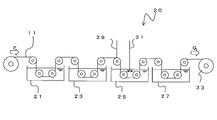
- FIG. 5 is a schematic view showing the wire tool manufacturing apparatus 20.
- the core wire 11 is manufactured. If the core wire 11 is a metal wire such as a piano wire, it can be used as it is. In the case of a non-metallic wire such as a glass wire, a conductive coating layer is provided on the outer peripheral surface in advance. In addition, also when using a piano wire, it is desirable to form copper plating etc. in an outer peripheral surface as mentioned above.
- the degreasing tank 21 is a tank in which, for example, an aqueous sodium hydroxide solution is stored, and dirt such as oil adhering to the outer surface of the core wire 11 is removed.
- the water rinsing tank 23 the chemical solution or the like in the degreasing tank 21 attached to the surface is washed.
- the plating tank 25 is a tank for performing electrolytic plating on the core wire 11 and electrodepositing the abrasive grains 13.
- the plating tank 25 is, for example, a nickel bath in which abrasive grains 13 are dispersed in a solution in which nickel is dissolved.
- an electrolytic bath adjusted to PH 4.0 using nickel sulfamate 300 g / l, nickel chloride 5 g / l, and boric acid 40 g / l can be used for the plating tank.
- the palladium coating 17 is formed in advance on the surface of the abrasive grain 13.
- a cathode 29 is connected to the core wire 11 passing through the plating tank 25.
- An anode 31 is immersed in the plating tank 25.
- the cathode 29 and the anode 31 are connected to a power source (not shown).
- the plating layer 15 having a desired thickness is formed.
- the abrasive grains 13 can be firmly held.
- the palladium coating 17 is formed in a sea shape on the surface of the abrasive grain 13
- the thickness of the plating layer 15 on the surface (tip portion) of the abrasive grain 13 is made larger than the thickness of the plating layer 15 on the surface of the core wire 11. It can be thinned to a predetermined ratio. For this reason, the cutting ability can be exhibited immediately from the initial use of the wire tool 7.
- the palladium coating 17 is formed in a sea shape, the palladium coating portion on the surface of the abrasive grain 13 is stably energized from the core wire 11 to the sea-like palladium coating 17 on the surface of the abrasive grain 13.
- the plating layer 15 is formed on the surface of the abrasive grain 13 at a substantially uniform speed. For this reason, even if the thickness of the plating layer 15 that holds the abrasive grains 13 is thin, a plating layer having a substantially uniform thickness is formed, and the abrasive grains 13 can be reliably held.
- the palladium coating 17 has excellent adhesion to nickel plating, the abrasive grains 13 can be reliably held by the plating layer 15.
- the area ratio of the sea part which is the palladium coating 17 is 70% or more and 90% or less, both the holding power of the abrasive grains 13 and the quality of the cut wafer can be kept good.
- the thickness of the palladium coating 17 is 0.01 ⁇ m to 0.5 ⁇ m, both the improvement of the adhesion with the plating layer 15 and the quality of the cut wafer can be kept good.
- the thickness of the plating layer 15 on the surface of the core wire 11 is less than 1 ⁇ 4 of the average particle size of the abrasive grains 13, the holding power is insufficient, but in the present invention, the thickness of the plating layer 15 on the surface of the core wire 11 is less than the abrasive grains 13. Since it is 1/4 or more of the average particle diameter, sufficient holding power of the abrasive grains 13 can be obtained. For this reason, dropping of the abrasive grains 13 during cutting can be suppressed. Moreover, since the thickness of the plating layer 15 is 3/4 or less of the average particle diameter of the abrasive grains 13, the plating layer 15 does not become too thick. The protrusion margin of the abrasive grains 13 from the plating layer 15 can be ensured. For this reason, tool life can be secured. Moreover, since it is not necessary to make the plating layer 15 excessively thick, productivity is good.
- the thickness of the plating layer 15 (abrasive plating layer) of the abrasive grain 13 at the portion protruding from the core wire plating layer is different from the thickness of the plating layer 15 (core wire plating layer) on the surface of the core wire 11 at a portion other than the abrasive grain 13. Since the ratio is 0.2 or more, sufficient holding power of the abrasive grains 13 can be obtained. In addition, since the ratio of the thickness of the abrasive plating layer to the thickness of the core wire plating layer is 0.8 or less, the cutting ability can be demonstrated in the initial use, and the processing time is shortened even when dressing is performed. can do.
- Example 1 The wire tool according to the present invention was manufactured as follows. Diamond abrasive grains were fixed to a piano wire with a diameter of 180 ⁇ m coated with about 1 ⁇ m of copper plating by nickel plating. A nickel sulfamate bath was used for nickel plating. Diamond abrasive grains having an average particle diameter of 35.2 ⁇ m were used.
- a cationic conditioner for example, a step of treating at 50 ° C. for 20 minutes (conditioner step), a step of immersing in a 50 ° C. solution in which a palladium compound is dissolved (activator step), and subsequent reduction. It can be obtained by combining three steps of a step (accelerator step) of immersing in a solution at a predetermined temperature in which a palladium compound containing an agent is dissolved for a predetermined time. In this way, the three steps, the number of treatments, the treatment time, etc. are set, and the palladium coating is applied to the diamond surface with an island-like covering state of 50 to 70%, a sea-like covering state of 50 to 90%, and a covering rate of 100%. It can be formed in various forms such as the entire surface covering state.
- the island-shaped covering state was obtained by repeatedly changing the number of times and time of the conditioner step and the activator step as appropriate, and then performing an accelerator step at a predetermined temperature of 50 ° C. ⁇ 20 minutes.
- the temperature of the accelerator process is set at a lower temperature for a longer time, for example, 40 ° C. ⁇ 60 minutes or more than when an island-like coating state is obtained.
- various sea-like coating states were obtained, and those having a full-surface covering state were set for the longest time.
- the diamond abrasive grains thus produced are added to a nickel sulfamate bath formed of nickel sulfamate, nickel chloride and boric acid, and the diamond abrasive grains are taken into the piano wire while being plated with nickel. A number of diamond abrasive grains were electrodeposited. Thereafter, in another nickel sulfamate bath, nickel plating was formed so that the plating thickness on the core wire was 17 ⁇ m, and the diamond was firmly fixed.
- the concentration of abrasive grains (number of abrasive grains per unit) of all wire tools according to Examples and Comparative Examples was set constant.
- the degree of abrasive grain concentration is the ratio of the area of the fixed abrasive grains to the projected area of the wire surface per predetermined length of wire, but the constant degree of abrasive grain concentration was used for the test. This is for performing equal evaluation of each example material and comparative example material.
- the one in which the palladium coating is formed in the sea shape is further processed by using the abrasive grains in which the palladium coating 17 is formed in an island shape, and further reducing the temperature of the accelerator treatment without repeating the conditioner step and the activator step.
- the palladium coating was grown and formed into a sea shape (No. 1 to No. 5 in Table 2).
- the surface of the diamond was completely covered with a film by further extending the accelerator treatment time (No.
- the palladium coverage was calculated by mapping the palladium on the surface of the diamond abrasive grains and calculating the area ratio from the binarized image. Also, the palladium coating thickness is calculated from the surface area when the amount of palladium adsorbed on the abrasive grains from the amount of liquid used is calculated by the atomic absorption method, assuming that the diamond abrasive grains are spheres, and using the above-described palladium coverage. The average thickness obtained.
- the metal core coating structure was assumed to be “sea-like”, and the palladium
- the coating state of the island is island-shaped, and the metal core coating structure is “island-shaped” for the form in which the coating state of palladium is divided into a plurality of parts with respect to the entire surface of the diamond abrasive grain,
- the metal core coating structure was defined as “entire surface” where palladium completely covered the surface of the diamond diamond grain.
- the core wire portion plating thickness is a plating thickness at a portion other than the diamond abrasive grains, and was measured by observing a cross section of the wire tool. Similarly, the plating thickness of the abrasive grains was measured.
- the plating thickness of an abrasive grain is the plating thickness (plating thickness formed on the palladium coating
- Abrasive plating thickness / core wire portion plating thickness was calculated from the obtained plating thickness of each part. Moreover, the plating thickness / abrasive grain size of the core wire portion was calculated.
- the diameter of the wire tool thus obtained was measured.
- a sapphire ingot ( ⁇ 2 inch, length of about 60 mm) was sliced.
- the cutting condition was reciprocating at a wire travel speed of 400 m / min, the workpiece was pressed at 0.3 mm / min, and the wire tool was processed while applying a water-soluble grinding fluid under a tension of 35 N. .
- the edge material was removed from the cut wafer, and the wafer thickness variation, TTV, warpage, surface roughness Ra, and the like were measured.
- the wafer thickness variation an average value of a total of five thicknesses of the center and four peripheral points of each wafer was calculated, and a standard deviation of the wafer thickness variation for all the wafers excluding the edge material was calculated.
- TTV conforms to “3.7.4 TV5” in the technical standard (QIAJ-B-007) defined by the Japan Quartz Device Industry Association. That is, TTV represents the parallelism between the front and back after the end of cutting.
- FIG. 6 is a diagram showing a measurement method of TTV (TV5).
- the center lines of the wafer perpendicular to the orientation flat (J in the figure) and secondary flat (K in the figure) of the obtained wafer are L and M, respectively.
- the thickness is 5 points in total, that is, H1 to H4 at the intersection of the line 6 mm inside from the outer periphery of the wafer (I in the figure) and the center lines L and M and H5 at the center of the wafer (intersection of the center lines L and M). Measure the thickness.
- the difference between the maximum value and the minimum value of the measured thickness becomes the measured value of TTV (TV5).
- the acceptance rate number of accepted wafers / number of measured wafers
- the warpage was evaluated by the difference between the maximum height and the minimum height by scanning the surface of the wafer with a flatness measuring device every five wafers cut out, and the average value was calculated.
- surface roughness Ra in the cutting direction (direction in which the wire tool bites) is measured with a stylus type surface roughness measuring instrument every five wafers cut out. The average value was used.
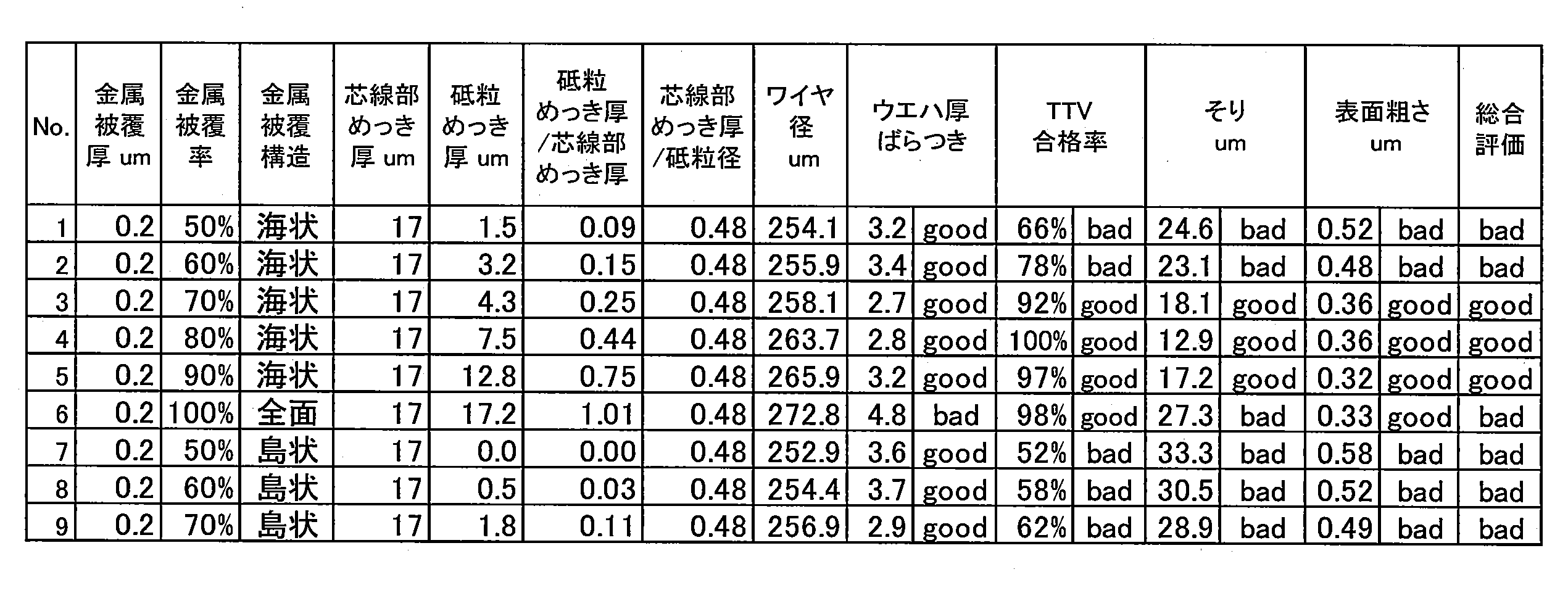
- Evaluation criteria are shown in Table 1, and each evaluation result is shown in Table 2.
- “Comprehensive evaluation” in Table 2 evaluated the four items of wafer thickness variation, TTV pass rate, warpage, and surface roughness according to the criteria shown in Table 1.
- the cutting property of the wire tool it is desirable that all of the above four items are excellent, and if any one of these four items has a low evaluation, it becomes a problem in practice.
- the lowest evaluation among the respective evaluations of each item is shown in the column of “Comprehensive evaluation” in Tables 2 to 6.
- No. 1 and N0.2 were evaluated as “bad” because the palladium coverage was low and not 70% to 90% despite the seawater palladium coating. No. In No. 6, since the palladium coating was coated over the entire surface of the diamond and the palladium coverage was 100%, the plating thickness of the abrasive grain surface was increased and the evaluation result was “bad”.
- the palladium coverage is preferably 70% to 90%.
- No. 7-No. No. 9 has an island-like coating structure in which the palladium coating is not sea-like, but is divided, so that uniform plating is not formed on the surface of the abrasive grains, and adhesion between the abrasive grains and the plating is insufficient.
- the abrasive grains easily fall off, the diameter of the wire tool is likely to change with time, and the plating thickness is not uniform, so that TTV and warpage deteriorated.
- No. No. 9 had a structure in which the abrasive grains were coated in an island shape in spite of a palladium coverage of 70%, so the evaluation result was “bad”.
- plating can be uniformly and stably formed on the abrasive grains, and the plating thickness on the abrasive grains can be increased.
- Abrasive grains can be firmly fixed while suppressing the quality of the wafer after cutting.
- Example 2 Next, No. 1 of Example 1 was used. 4 was used as a reference, and the same evaluation was performed by changing the palladium coating thickness on the abrasive grains. The results are shown in Table 3. Except for the palladium coating thickness, No. 1 in Example 1 was used. The same as 4. In addition, No. 1 of Example 1 was used. 4 and No. 2 of Example 2. 16 is the same sample.
- the palladium coating thickness can be changed as appropriate by changing the temperature of the accelerator treatment. Specifically, the coating thickness was adjusted from 0.002 ⁇ m to 0.8 ⁇ m by changing the processing temperature at the time of accelerator treatment using abrasive grains in which a palladium coating was formed in an island shape on the abrasive grain surface (No .11 to No. 20).
- Table 3 shows that the palladium coating thickness is in the range of 0.01 to 0.5 ⁇ m, and the abrasive plating thickness / core wire plating thickness is in the range of 0.2 to 0.8. 13-No. 18 had an evaluation of “good”. No. 19, no. When the palladium coating thickness was 0.6 ⁇ m or more as in 20, the evaluation was “bad”. This is because the palladium coating is thick, so that the abrasive grains are firmly fixed, but the plating on the abrasive grains is also thickened. As a result, the variation in the wafer thickness is increased due to the sliding of the wire tool particularly in the initial stage of cutting.
- the palladium coating thickness of the abrasive grains is desirably 0.01 to 0.5 ⁇ m.
- Example 3 Next, the same evaluation was performed by changing the plating thickness of the core wire portion. The results are shown in Table 4. In addition, No. of Example 1 except the plating thickness of a core wire part. The same as 4. The plating thickness of the core wire part was adjusted by the applied current and the plating time.
- the core wire portion plating thickness is 10 ⁇ m to 26 ⁇ m, and the core wire portion plating thickness / abrasive grain size is in the range of 0.25 to 0.75 (that is, the core wire portion plating thickness / abrasive grain size is 0.25 to 0.75). No. range). 22-No. 25, the evaluation was “good”.
- the core wire plating thickness / abrasive grain size is 0.20. 21 had an evaluation of “bad”. This is because the holding power of the abrasive grains is insufficient because the plating thickness is too thin. As a result, the abrasive grains easily fall off, the diameter of the wire tool easily changes with time, and TTV and warpage deteriorate.
- the core wire portion plating thickness / abrasive grain size is desirably 0.25 to 0.75.
- Example 4 diamond abrasive grains having an abrasive grain size of 9.8 ⁇ m were used, and the same evaluation as in Example 1 was performed by changing the palladium coverage. The results are shown in Table 5.
- the plating thickness of the core wire portion was 6 ⁇ m.
- the palladium coating thickness is the same as in Example 1. In addition, it experimented by changing the cutting speed suitably according to the size of an abrasive grain.
- the palladium coating was in the sea state (diamond exposed portion was island-shaped), and the palladium coverage was in the range of 70% to 90%, so uniform plating was also formed on the abrasive grain surface. As a result, the evaluation result was “good”.
- No. 33 no. No. 34 has a palladium coverage as low as 50 to 60% even though the palladium coating is sea-like, so that the thickness of the abrasive plating is thin, the adhesion to the abrasive is low, and the abrasive tends to fall off. became. For this reason, the diameter of the wire tool changed with time, and TTV and warpage deteriorated. As a result, the evaluation result was “bad”.
- the coverage of palladium is 70%, but since the palladium coating is coated in an island-like manner rather than in the sea, uniform plating is not formed on the surface of the abrasive grains, and the abrasive grains and the plating Insufficient adhesion. As a result, the abrasive grains easily fall off, the diameter of the wire tool easily changes with time, and TTV and warpage deteriorate.
- Example 5 diamond abrasive grains having an abrasive grain size of 58.7 ⁇ m were used, and the same evaluation as in Example 4 was performed by changing the palladium coverage. The results are shown in Table 6. In addition, the plating thickness of the core part was 30 ⁇ m. The palladium coating thickness is the same as in Example 1. In addition, it experimented by changing the cutting speed suitably according to the size of an abrasive grain.
- No. No. 46 has a palladium coverage of 70%, but the palladium coating is not sea-like but is island-like, so that uniform plating is not formed on the surface of the abrasive grains. Insufficient adhesion. As a result, the abrasive grains easily fall off, the diameter of the wire tool easily changes with time, and TTV and warpage deteriorate.
- the metal that coats the surface of the abrasive grains is palladium, and in addition to the coverage and the coating thickness, the coating structure is limited, so that the abrasive grains can be applied to the plating thickness on the core wire regardless of the size of the abrasive grain size.
- the plating thickness can be set within an appropriate range. Thereby, it becomes a wire tool which can exhibit the initial sharpness while firmly fixing the abrasive grains, and can satisfy all the wafer qualities.
Abstract
Description
以下、図面を参照しながら、本発明の実施形態について説明する。図1は、切断装置1を示す概略図である。切断装置1は、切断対象物であるインゴット3をスライス加工するものである。切断装置1には、インゴット3を保持する保持部5と、ワイヤ工具7を移動させるための多溝を有するローラ9と、保持部5およびローラ9を駆動するための図示を省略したモータ等から構成される。 (Cutting device)
Hereinafter, embodiments of the present invention will be described with reference to the drawings. FIG. 1 is a schematic view showing a
次に、ワイヤ工具7について説明する。図2はワイヤ工具7の軸方向に垂直な方向の断面を示す図である。ワイヤ工具7は、主に芯線11、砥粒13、めっき層15等から構成される。 (Wire tool)
Next, the
芯線11は、高強度で導電性を有する金属線である。芯線11としては、例えばピアノ線、ステンレス鋼線、タングステン線、モリブデン線などを用いることができる。また、芯線11としては、ガラスファイバ、アラミド繊維、炭素繊維、アルミナ繊維、ボロン繊維などの非金属線に導電性被覆層を形成したものも適用することができる。 (Core wire 11)
The core wire 11 is a metal wire having high strength and conductivity. As the core wire 11, for example, a piano wire, a stainless steel wire, a tungsten wire, a molybdenum wire, or the like can be used. Further, as the core wire 11, a non-metallic wire such as glass fiber, aramid fiber, carbon fiber, alumina fiber, boron fiber, etc., on which a conductive coating layer is formed can be applied.
芯線11の外周には、砥粒13が固定される。砥粒13はダイヤモンド砥粒である。すなわち、砥粒13はワイヤ工具用のダイヤモンド砥粒である。砥粒13の平均粒径は、5μm~70μmであることが望ましく、10~60μmであることがさらに望ましい。砥粒13の粒径が小さすぎると、切削能力が劣る。また、砥粒13の粒径が大きすぎると、これを保持するための砥粒保持層の厚みを厚くする必要があることから、ワイヤ工具7の外径が大きくなり歩留まりが低下するためである。 (Abrasive grain 13)
めっき層15は、芯線11の外周に形成され、砥粒13の保持層として機能する。めっき層15としては、砥粒13を保持できればいずれの金属でも良いが、ニッケル、またはその合金からなるめっきがもっとも好ましい。めっき層15の厚みは、砥粒13の平均粒径に応じて設定される。なお、めっき層15は芯線11の表面を覆う芯線めっき層と、砥粒13の表面を覆う砥粒めっき層からなる。 (Plating layer 15)
The
図4A~図4Cは、砥粒13の概念図であり、図4Aは処理前のダイヤモンド粒子14を示す図であり、図4Bは、ダイヤモンド粒子14の表面に海状にパラジウム被覆を施した状態を示す図であり、図4Cは、ダイヤモンド粒子14の表面に島状にパラジウム被覆を施した状態を示す図である。砥粒13を芯線11に付着させる前に、砥粒13の表面には、パラジウム被覆17が施される。なお、ダイヤモンド砥粒の表面に形成される金属膜は、ニッケルやチタンを用いることもできるが、ニッケルやチタンは表面に不動態膜を形成するため、めっき層15との密着力が低下し、砥粒13の保持力が不十分になる可能性がある。これに対し、パラジウムは、不動態膜を形成しないためニッケルめっきとの密着性が良い。したがって、ダイヤモンド粒子の下地被覆としては、パラジウム被覆が好ましい。 (Surface properties of abrasive grains 13)
4A to 4C are conceptual diagrams of the
このような、砥粒表面へのパラジウム被覆17の形成方法としては、例えば、以下のようにして行うことができる。 (Method of forming palladium metal core coating on abrasive grain surface)
Such a method of forming the
まず、ダイヤモンド粒子14の表面の電位を調整し、正電荷を付与する。具体的には、アミン塩系化合物など一般的に用いられるカチオン界面活性剤を用いて表面の処理を行う。
アクチベーター工程:
次に、パラジウム粒子(化合物)をダイヤモンド粒子14の表面に吸着させる。パラジウム化合物としては公知の物を使用可能で、例えば、塩化パラジウム、硝酸パラジウム、硫酸パラジウム、酢酸パラジウム、酸化パラジウム、などの水溶性パラジウム化合物である。この際、ダイヤモンド粒子14の表面に、コンディショナー工程とアクチベーター工程とを後述する所定の条件にて繰り返すことでパラジウム金属化合物を無数に吸着させる。この処理を繰り返す、もしくは処理液のパラジウム濃度をあげることにより、パラジウムの付着量は増加していき、ダイヤモンド砥粒表面において、パラジウム金属核の被覆状態は島状に成長していく。
アクセレレータ工程:
最後に、付着したパラジウム核を金属皮膜化させる方向に成長させる。具体的には、還元処理を行う。本工程を行うことで、アクチベーター工程で吸着したパラジウム化合物を還元処理することでパラジウム金属核が互い連続的に配列する構造を取ることになり、パラジウムを海状に形成することが容易になる。なお、被覆率に関しては処理時間を調整することで調整することが可能である。また、膜厚の調整は処理温度を変更し、還元反応の速度を調整し行うことができ、反応速度が速くなることで膜が厚くなる方向に進む。 Conditioner process:
First, the surface potential of the
Activator process:
Next, palladium particles (compound) are adsorbed on the surfaces of the
Accelerator process:
Finally, the deposited palladium nuclei are grown in the direction of forming a metal film. Specifically, a reduction process is performed. By carrying out this process, the palladium compound adsorbed in the activator process is reduced, so that the palladium metal nuclei are arranged in a continuous manner, and it becomes easy to form palladium in a sea state. . Note that the coverage can be adjusted by adjusting the processing time. In addition, the film thickness can be adjusted by changing the processing temperature and adjusting the reduction reaction speed, and the reaction speed increases and the film becomes thicker.
次に、ワイヤ工具7の製造工程を説明する。図5は、ワイヤ工具製造装置20を示す概略図である。まず、芯線11を製造する。芯線11は、例えばピアノ線などの金属線であれば、そのまま使用することができる。また、ガラス線などの非金属線の場合には、あらかじめ外周面に導電性被覆層が設けられる。なお、ピアノ線を用いる場合にも、前述したように、外周面に銅めっき等を形成しておくことが望ましい。 (Wire tool manufacturing method)
Next, the manufacturing process of the
本発明にかかるワイヤ工具は、以下のように製造した。約1μmの銅めっきが被覆された直径180μmのピアノ線に、ダイヤモンド砥粒をニッケルめっきで固着した。ニッケルめっきにはスルファミン酸ニッケル浴を用いた。ダイヤモンド砥粒は、平均粒径35.2μmのものを用いた。 Example 1
The wire tool according to the present invention was manufactured as follows. Diamond abrasive grains were fixed to a piano wire with a diameter of 180 μm coated with about 1 μm of copper plating by nickel plating. A nickel sulfamate bath was used for nickel plating. Diamond abrasive grains having an average particle diameter of 35.2 μm were used.

次に、実施例1のNo.4を基準として、砥粒上のパラジウム被覆厚を変化させて同様の評価を行った。結果を表3に示す。なお、パラジウム被覆厚以外については、実施例1のNo.4と同様である。また、実施例1のNo.4と実施例2のNo.16は同じサンプルである。 (Example 2)
Next, No. 1 of Example 1 was used. 4 was used as a reference, and the same evaluation was performed by changing the palladium coating thickness on the abrasive grains. The results are shown in Table 3. Except for the palladium coating thickness, No. 1 in Example 1 was used. The same as 4. In addition, No. 1 of Example 1 was used. 4 and No. 2 of Example 2. 16 is the same sample.

次に、芯線部のめっき厚を変化させて同様の評価を行った。結果を表4に示す。なお、芯線部のめっき厚以外は、実施例1のNo.4と同様である。芯線部のめっき厚は、印加電流とめっき時間で調整した。 (Example 3)
Next, the same evaluation was performed by changing the plating thickness of the core wire portion. The results are shown in Table 4. In addition, No. of Example 1 except the plating thickness of a core wire part. The same as 4. The plating thickness of the core wire part was adjusted by the applied current and the plating time.

次に、砥粒径が9.8μmのダイヤモンド砥粒を用い、パラジウム被覆率を変化させて実施例1と同様の評価を行った。結果を表5に示す。なお、芯線部のめっき厚は、6μmとした。パラジウム被覆厚については、実施例1と同様である。なお、砥粒のサイズに応じ、切断速度を適宜変更して実験を行った。 (Example 4)
Next, diamond abrasive grains having an abrasive grain size of 9.8 μm were used, and the same evaluation as in Example 1 was performed by changing the palladium coverage. The results are shown in Table 5. The plating thickness of the core wire portion was 6 μm. The palladium coating thickness is the same as in Example 1. In addition, it experimented by changing the cutting speed suitably according to the size of an abrasive grain.

次に、砥粒径が58.7μmのダイヤモンド砥粒を用い、パラジウム被覆率を変化させて実施例4と同様の評価を行った。結果を表6に示す。なお、芯線部のめっき厚は、30μmとした。パラジウム被覆厚については、実施例1と同様である。なお、砥粒のサイズに応じ、切断速度を適宜変更して実験を行った。 (Example 5)
Next, diamond abrasive grains having an abrasive grain size of 58.7 μm were used, and the same evaluation as in Example 4 was performed by changing the palladium coverage. The results are shown in Table 6. In addition, the plating thickness of the core part was 30 μm. The palladium coating thickness is the same as in Example 1. In addition, it experimented by changing the cutting speed suitably according to the size of an abrasive grain.

3………インゴット
5………保持部
7………ワイヤ工具
9………ローラ
11………芯線
13………砥粒
14………ダイヤモンド粒子
15………めっき層
15a………芯線めっき層
15b………砥粒めっき層
17………パラジウム被覆
18………ダイヤモンド露出部
20………ワイヤ工具製造装置
21………脱脂槽
23………水洗槽
25………めっき槽
27………水洗槽
29………陰極
31………陽極
33………巻き取り装置 DESCRIPTION OF
Claims (5)
- ダイヤモンド粒子の表面の一部がパラジウムで被覆されたダイヤモンド砥粒であって、
前記ダイヤモンド粒子の表面にパラジウムが被覆厚さ0.01μmから0.5μmの厚さにて略連続被覆された海部と、前記ダイヤモンド粒子の表面がパラジウムで被覆されずに前記ダイヤモンド粒子の表面が露出する露出部とから構成され、
前記海部の面積率が前記ダイヤモンド粒子の表面積の70%以上90%以下で、残部が前記露出部であることを特徴とするワイヤ工具用ダイヤモンド砥粒。 Diamond abrasive grains in which a part of the surface of the diamond particles is coated with palladium,
A sea part in which palladium is coated on the surface of the diamond particles with a coating thickness of 0.01 μm to 0.5 μm, and the surface of the diamond particles is exposed without being coated with palladium. And an exposed part that
The diamond abrasive grain for a wire tool, wherein an area ratio of the sea part is 70% or more and 90% or less of a surface area of the diamond particle, and the remaining part is the exposed part. - 請求項1に記載のダイヤモンド砥粒と、導電性を有する芯線と、前記芯線の外周に形成され、前記ダイヤモンド砥粒を保持するめっき層とを具備し、
前記めっき層は前記芯線の表面を覆う芯線めっき層と、前記ダイヤモンド砥粒の表面を覆う砥粒めっき層からなり、
前記芯線めっき層から突出している部位の前記ダイヤモンド砥粒の表面における前記砥粒めっき層の平均厚みが、前記芯線めっき層の平均厚みに対し、0.2以上0.8以下であることを特徴とするワイヤ工具。 The diamond abrasive grain according to claim 1, comprising a conductive core wire, and a plating layer formed on an outer periphery of the core wire and holding the diamond abrasive grain,
The plating layer is composed of a core wire plating layer covering the surface of the core wire and an abrasive plating layer covering the surface of the diamond abrasive grain,
The average thickness of the abrasive plating layer on the surface of the diamond abrasive grain at the portion protruding from the core wire plating layer is 0.2 or more and 0.8 or less with respect to the average thickness of the core wire plating layer. Wire tool. - 請求項1に記載のダイヤモンド砥粒と、導電性を有する芯線と、前記芯線の外周に形成され、前記ダイヤモンド砥粒を保持するめっき層とを具備し、
前記めっき層は前記芯線の表面を覆う芯線めっき層と、前記ダイヤモンド砥粒の表面を覆う砥粒めっき層からなり、
前記ダイヤモンド砥粒の先端部の前記砥粒めっき層の一部が除去され、少なくとも一部の前記ダイヤモンド砥粒の先端の一部が露出していることを特徴とするワイヤ工具。 The diamond abrasive grain according to claim 1, comprising a conductive core wire, and a plating layer formed on an outer periphery of the core wire and holding the diamond abrasive grain,
The plating layer is composed of a core wire plating layer covering the surface of the core wire and an abrasive plating layer covering the surface of the diamond abrasive grain,
A wire tool, wherein a part of the abrasive plating layer at the tip of the diamond abrasive is removed, and at least a part of the tip of the diamond abrasive is exposed. - 前記芯線めっき層の平均厚みが前記ダイヤモンド砥粒の平均粒径の0.25倍以上0.75倍以下であることを特徴とする請求項2または請求項3に記載のワイヤ工具。 The wire tool according to claim 2 or 3, wherein an average thickness of the core wire plating layer is not less than 0.25 times and not more than 0.75 times the average particle diameter of the diamond abrasive grains.
- 前記芯線の表面にストライクめっき層を有することを特徴とする請求項2または請求項3に記載のワイヤ工具。 The wire tool according to claim 2 or 3, further comprising a strike plating layer on a surface of the core wire.
Priority Applications (5)
| Application Number | Priority Date | Filing Date | Title |
|---|---|---|---|
| EP16851053.5A EP3357642A4 (en) | 2015-09-30 | 2016-09-06 | Abrasive diamond grain for wire tool and wire tool |
| KR1020187011704A KR102135652B1 (en) | 2015-09-30 | 2016-09-06 | Diamond abrasive and wire tools for wire tools |
| JP2017543054A JP6452837B2 (en) | 2015-09-30 | 2016-09-06 | Diamond abrasive for wire tools and wire tools |
| CN201680055701.2A CN108136567B (en) | 2015-09-30 | 2016-09-06 | Diamond abrasive grain for wire tool and wire tool |
| US15/937,435 US20180215074A1 (en) | 2015-09-30 | 2018-03-27 | Abrasive diamond grain for wire tool and wire tool |
Applications Claiming Priority (2)
| Application Number | Priority Date | Filing Date | Title |
|---|---|---|---|
| JP2015193554 | 2015-09-30 | ||
| JP2015-193554 | 2015-09-30 |
Related Child Applications (1)
| Application Number | Title | Priority Date | Filing Date |
|---|---|---|---|
| US15/937,435 Continuation US20180215074A1 (en) | 2015-09-30 | 2018-03-27 | Abrasive diamond grain for wire tool and wire tool |
Publications (1)
| Publication Number | Publication Date |
|---|---|
| WO2017056877A1 true WO2017056877A1 (en) | 2017-04-06 |
Family
ID=58427473
Family Applications (1)
| Application Number | Title | Priority Date | Filing Date |
|---|---|---|---|
| PCT/JP2016/076188 WO2017056877A1 (en) | 2015-09-30 | 2016-09-06 | Abrasive diamond grain for wire tool and wire tool |
Country Status (7)
| Country | Link |
|---|---|
| US (1) | US20180215074A1 (en) |
| EP (1) | EP3357642A4 (en) |
| JP (1) | JP6452837B2 (en) |
| KR (1) | KR102135652B1 (en) |
| CN (1) | CN108136567B (en) |
| TW (1) | TWI636841B (en) |
| WO (1) | WO2017056877A1 (en) |
Cited By (1)
| Publication number | Priority date | Publication date | Assignee | Title |
|---|---|---|---|---|
| CN107599193A (en) * | 2017-05-24 | 2018-01-19 | 浙江好亚能源股份有限公司 | Using the monocrystalline silicon piece slicer of golden steel wire hi-precision cutting |
Families Citing this family (3)
| Publication number | Priority date | Publication date | Assignee | Title |
|---|---|---|---|---|
| JP6693460B2 (en) * | 2017-04-04 | 2020-05-13 | 信越半導体株式会社 | Work cutting method |
| DE102018221921A1 (en) * | 2018-12-17 | 2020-06-18 | Siltronic Ag | Method for manufacturing semiconductor wafers using a wire saw |
| JP7103305B2 (en) * | 2019-05-29 | 2022-07-20 | 信越半導体株式会社 | How to cut the ingot |
Citations (4)
| Publication number | Priority date | Publication date | Assignee | Title |
|---|---|---|---|---|
| JP2010120116A (en) * | 2008-11-19 | 2010-06-03 | Read Co Ltd | Fixed abrasive grain wire saw |
| WO2011042931A1 (en) * | 2009-10-06 | 2011-04-14 | ジャパンファインスチール株式会社 | Fixed abrasive grain wire, process for producing the fixed abrasive grain wire, and abrasive grains for use in fixed abrasive grain wire |
| JP2013136142A (en) * | 2011-12-02 | 2013-07-11 | Furukawa Electric Co Ltd:The | Manufacturing method of diamond abrasive grain, manufacturing method of wire tool and wire tool |
| JP2014188655A (en) * | 2013-03-28 | 2014-10-06 | Furukawa Electric Co Ltd:The | Wire tool for polycrystalline silicon cutting and polycrystalline silicon cutting method |
Family Cites Families (13)
| Publication number | Priority date | Publication date | Assignee | Title |
|---|---|---|---|---|
| JPS4724779Y1 (en) | 1967-04-07 | 1972-08-04 | ||
| DE2434816C3 (en) | 1974-07-19 | 1981-01-22 | Basf Ag, 6700 Ludwigshafen | Process for the production of nitrogen-containing condensation products and their use as retention aids, flocculants and dewatering accelerators in paper manufacture |
| KR100818905B1 (en) * | 2003-05-09 | 2008-04-03 | 다이아몬드 이노베이션즈, 인크. | Abrasive particles having coatings with tortuous surface topography |
| JP4139810B2 (en) | 2004-12-28 | 2008-08-27 | 旭ダイヤモンド工業株式会社 | Electrodeposition wire tool |
| TW201111106A (en) * | 2009-03-02 | 2011-04-01 | Sumitomo Electric Industries | Diamond wire saw, process for manufacturing diamond wire saw |
| MX2012001810A (en) * | 2009-08-14 | 2012-06-01 | Saint Gobain Abrasives Inc | Abrasive articles including abrasive particles bonded to an elongated body. |
| TW201226097A (en) * | 2010-12-24 | 2012-07-01 | Micron Diamond Wire & Equipment Co Ltd | Diamond wire structure |
| TW201317101A (en) * | 2011-10-26 | 2013-05-01 | Taiwan Union Abrasives Corp | Diamond wire saw |
| TW201325780A (en) * | 2011-12-16 | 2013-07-01 | pei-song Zhou | Diamond nickel-cobalt jigsaw and production method |
| JP6352176B2 (en) * | 2012-05-31 | 2018-07-04 | 株式会社リード | Fixed abrasive wire saw, manufacturing method thereof, and work cutting method using the same |
| TWI474889B (en) * | 2012-06-29 | 2015-03-01 | Saint Gobain Abrasives Inc | Abrasive article and method of forming |
| JP2014172115A (en) * | 2013-03-07 | 2014-09-22 | Noritake Co Ltd | Fixed abrasive grain wire, and method for production thereof |
| CN203344192U (en) * | 2013-06-07 | 2013-12-18 | 厦门致力金刚石科技股份有限公司 | Small-diameter diamond wire saw structure |
-
2016
- 2016-09-06 KR KR1020187011704A patent/KR102135652B1/en active IP Right Grant
- 2016-09-06 JP JP2017543054A patent/JP6452837B2/en not_active Expired - Fee Related
- 2016-09-06 CN CN201680055701.2A patent/CN108136567B/en active Active
- 2016-09-06 WO PCT/JP2016/076188 patent/WO2017056877A1/en active Application Filing
- 2016-09-06 EP EP16851053.5A patent/EP3357642A4/en not_active Withdrawn
- 2016-09-12 TW TW105129619A patent/TWI636841B/en active
-
2018
- 2018-03-27 US US15/937,435 patent/US20180215074A1/en not_active Abandoned
Patent Citations (4)
| Publication number | Priority date | Publication date | Assignee | Title |
|---|---|---|---|---|
| JP2010120116A (en) * | 2008-11-19 | 2010-06-03 | Read Co Ltd | Fixed abrasive grain wire saw |
| WO2011042931A1 (en) * | 2009-10-06 | 2011-04-14 | ジャパンファインスチール株式会社 | Fixed abrasive grain wire, process for producing the fixed abrasive grain wire, and abrasive grains for use in fixed abrasive grain wire |
| JP2013136142A (en) * | 2011-12-02 | 2013-07-11 | Furukawa Electric Co Ltd:The | Manufacturing method of diamond abrasive grain, manufacturing method of wire tool and wire tool |
| JP2014188655A (en) * | 2013-03-28 | 2014-10-06 | Furukawa Electric Co Ltd:The | Wire tool for polycrystalline silicon cutting and polycrystalline silicon cutting method |
Non-Patent Citations (1)
| Title |
|---|
| See also references of EP3357642A4 * |
Cited By (1)
| Publication number | Priority date | Publication date | Assignee | Title |
|---|---|---|---|---|
| CN107599193A (en) * | 2017-05-24 | 2018-01-19 | 浙江好亚能源股份有限公司 | Using the monocrystalline silicon piece slicer of golden steel wire hi-precision cutting |
Also Published As
| Publication number | Publication date |
|---|---|
| CN108136567B (en) | 2020-06-16 |
| EP3357642A4 (en) | 2019-05-29 |
| TWI636841B (en) | 2018-10-01 |
| EP3357642A1 (en) | 2018-08-08 |
| KR20180063168A (en) | 2018-06-11 |
| JPWO2017056877A1 (en) | 2018-06-07 |
| JP6452837B2 (en) | 2019-01-16 |
| CN108136567A (en) | 2018-06-08 |
| KR102135652B1 (en) | 2020-07-20 |
| TW201714690A (en) | 2017-05-01 |
| US20180215074A1 (en) | 2018-08-02 |
Similar Documents
| Publication | Publication Date | Title |
|---|---|---|
| KR101194113B1 (en) | Electrodeposited wire tool and method of producing same | |
| JP6452837B2 (en) | Diamond abrasive for wire tools and wire tools | |
| JP6352176B2 (en) | Fixed abrasive wire saw, manufacturing method thereof, and work cutting method using the same | |
| JP2009066689A (en) | Fixed abrasive grain wire saw | |
| JP5356071B2 (en) | Diamond wire saw, diamond wire saw manufacturing method | |
| JP2007152485A (en) | Manufacturing method of saw wire | |
| EP2424702A1 (en) | A fixed abrasive sawing wire with a rough interface between core and outer sheath | |
| JP5066508B2 (en) | Fixed abrasive wire saw | |
| JP5705813B2 (en) | Diamond abrasive manufacturing method, wire tool manufacturing method, and wire tool | |
| KR20010055980A (en) | Wire saw with adhesive diamond electrodeposited on it and its manufacturing method | |
| JP2014188655A (en) | Wire tool for polycrystalline silicon cutting and polycrystalline silicon cutting method | |
| TWI552820B (en) | A fixed abrasive sawing wire and producing method thereof | |
| JP2011255475A (en) | Fixed abrasive wire | |
| JP6329796B2 (en) | Manufacturing method of wire tool | |
| JP4470559B2 (en) | Ultra-thin blade and manufacturing method thereof | |
| KR20140095205A (en) | Wire cutting tool comprising different kind of abrasive particles, and method of fabricating the same | |
| CN104955601B (en) | There is the fixed abrasive sawline at nickel oxide interface between nickel subgrade | |
| JP2010052070A (en) | Electrodeposition bonded abrasive tool, method of manufacturing the same, and abrasive grain used for manufacturing the same | |
| JP2022165654A (en) | electroformed blade | |
| CN112059933A (en) | Ring-shaped grinding tool | |
| KR20090131531A (en) | A wire saw | |
| JP2018507788A (en) | Method for producing fixed abrasive saw wire having metal alloy fixed layer and wire obtained thereby |
Legal Events
| Date | Code | Title | Description |
|---|---|---|---|
| 121 | Ep: the epo has been informed by wipo that ep was designated in this application |
Ref document number: 16851053 Country of ref document: EP Kind code of ref document: A1 |
|
| ENP | Entry into the national phase |
Ref document number: 2017543054 Country of ref document: JP Kind code of ref document: A |
|
| NENP | Non-entry into the national phase |
Ref country code: DE |
|
| ENP | Entry into the national phase |
Ref document number: 20187011704 Country of ref document: KR Kind code of ref document: A |
|
| WWE | Wipo information: entry into national phase |
Ref document number: 2016851053 Country of ref document: EP |