WO2017056784A1 - 撮像装置、内視鏡および内視鏡システム - Google Patents
撮像装置、内視鏡および内視鏡システム Download PDFInfo
- Publication number
- WO2017056784A1 WO2017056784A1 PCT/JP2016/074413 JP2016074413W WO2017056784A1 WO 2017056784 A1 WO2017056784 A1 WO 2017056784A1 JP 2016074413 W JP2016074413 W JP 2016074413W WO 2017056784 A1 WO2017056784 A1 WO 2017056784A1
- Authority
- WO
- WIPO (PCT)
- Prior art keywords
- unit
- pixel
- light
- filter
- pixels
- Prior art date
- Legal status (The legal status is an assumption and is not a legal conclusion. Google has not performed a legal analysis and makes no representation as to the accuracy of the status listed.)
- Ceased
Links
Images







Classifications
-
- A—HUMAN NECESSITIES
- A61—MEDICAL OR VETERINARY SCIENCE; HYGIENE
- A61B—DIAGNOSIS; SURGERY; IDENTIFICATION
- A61B1/00—Instruments for performing medical examinations of the interior of cavities or tubes of the body by visual or photographical inspection, e.g. endoscopes; Illuminating arrangements therefor
- A61B1/06—Instruments for performing medical examinations of the interior of cavities or tubes of the body by visual or photographical inspection, e.g. endoscopes; Illuminating arrangements therefor with illuminating arrangements
- A61B1/0638—Instruments for performing medical examinations of the interior of cavities or tubes of the body by visual or photographical inspection, e.g. endoscopes; Illuminating arrangements therefor with illuminating arrangements providing two or more wavelengths
-
- A—HUMAN NECESSITIES
- A61—MEDICAL OR VETERINARY SCIENCE; HYGIENE
- A61B—DIAGNOSIS; SURGERY; IDENTIFICATION
- A61B1/00—Instruments for performing medical examinations of the interior of cavities or tubes of the body by visual or photographical inspection, e.g. endoscopes; Illuminating arrangements therefor
- A61B1/00002—Operational features of endoscopes
- A61B1/00004—Operational features of endoscopes characterised by electronic signal processing
- A61B1/00006—Operational features of endoscopes characterised by electronic signal processing of control signals
-
- A—HUMAN NECESSITIES
- A61—MEDICAL OR VETERINARY SCIENCE; HYGIENE
- A61B—DIAGNOSIS; SURGERY; IDENTIFICATION
- A61B1/00—Instruments for performing medical examinations of the interior of cavities or tubes of the body by visual or photographical inspection, e.g. endoscopes; Illuminating arrangements therefor
- A61B1/00002—Operational features of endoscopes
- A61B1/00004—Operational features of endoscopes characterised by electronic signal processing
- A61B1/00009—Operational features of endoscopes characterised by electronic signal processing of image signals during a use of endoscope
-
- A—HUMAN NECESSITIES
- A61—MEDICAL OR VETERINARY SCIENCE; HYGIENE
- A61B—DIAGNOSIS; SURGERY; IDENTIFICATION
- A61B1/00—Instruments for performing medical examinations of the interior of cavities or tubes of the body by visual or photographical inspection, e.g. endoscopes; Illuminating arrangements therefor
- A61B1/00163—Optical arrangements
- A61B1/00186—Optical arrangements with imaging filters
-
- A—HUMAN NECESSITIES
- A61—MEDICAL OR VETERINARY SCIENCE; HYGIENE
- A61B—DIAGNOSIS; SURGERY; IDENTIFICATION
- A61B1/00—Instruments for performing medical examinations of the interior of cavities or tubes of the body by visual or photographical inspection, e.g. endoscopes; Illuminating arrangements therefor
- A61B1/04—Instruments for performing medical examinations of the interior of cavities or tubes of the body by visual or photographical inspection, e.g. endoscopes; Illuminating arrangements therefor combined with photographic or television appliances
- A61B1/045—Control thereof
-
- A—HUMAN NECESSITIES
- A61—MEDICAL OR VETERINARY SCIENCE; HYGIENE
- A61B—DIAGNOSIS; SURGERY; IDENTIFICATION
- A61B1/00—Instruments for performing medical examinations of the interior of cavities or tubes of the body by visual or photographical inspection, e.g. endoscopes; Illuminating arrangements therefor
- A61B1/04—Instruments for performing medical examinations of the interior of cavities or tubes of the body by visual or photographical inspection, e.g. endoscopes; Illuminating arrangements therefor combined with photographic or television appliances
- A61B1/05—Instruments for performing medical examinations of the interior of cavities or tubes of the body by visual or photographical inspection, e.g. endoscopes; Illuminating arrangements therefor combined with photographic or television appliances characterised by the image sensor, e.g. camera, being in the distal end portion
- A61B1/051—Details of CCD assembly
-
- A—HUMAN NECESSITIES
- A61—MEDICAL OR VETERINARY SCIENCE; HYGIENE
- A61B—DIAGNOSIS; SURGERY; IDENTIFICATION
- A61B1/00—Instruments for performing medical examinations of the interior of cavities or tubes of the body by visual or photographical inspection, e.g. endoscopes; Illuminating arrangements therefor
- A61B1/06—Instruments for performing medical examinations of the interior of cavities or tubes of the body by visual or photographical inspection, e.g. endoscopes; Illuminating arrangements therefor with illuminating arrangements
- A61B1/0646—Instruments for performing medical examinations of the interior of cavities or tubes of the body by visual or photographical inspection, e.g. endoscopes; Illuminating arrangements therefor with illuminating arrangements with illumination filters
-
- A—HUMAN NECESSITIES
- A61—MEDICAL OR VETERINARY SCIENCE; HYGIENE
- A61B—DIAGNOSIS; SURGERY; IDENTIFICATION
- A61B1/00—Instruments for performing medical examinations of the interior of cavities or tubes of the body by visual or photographical inspection, e.g. endoscopes; Illuminating arrangements therefor
- A61B1/06—Instruments for performing medical examinations of the interior of cavities or tubes of the body by visual or photographical inspection, e.g. endoscopes; Illuminating arrangements therefor with illuminating arrangements
- A61B1/0655—Control therefor
-
- A—HUMAN NECESSITIES
- A61—MEDICAL OR VETERINARY SCIENCE; HYGIENE
- A61B—DIAGNOSIS; SURGERY; IDENTIFICATION
- A61B1/00—Instruments for performing medical examinations of the interior of cavities or tubes of the body by visual or photographical inspection, e.g. endoscopes; Illuminating arrangements therefor
- A61B1/06—Instruments for performing medical examinations of the interior of cavities or tubes of the body by visual or photographical inspection, e.g. endoscopes; Illuminating arrangements therefor with illuminating arrangements
- A61B1/07—Instruments for performing medical examinations of the interior of cavities or tubes of the body by visual or photographical inspection, e.g. endoscopes; Illuminating arrangements therefor with illuminating arrangements using light-conductive means, e.g. optical fibres
-
- H—ELECTRICITY
- H04—ELECTRIC COMMUNICATION TECHNIQUE
- H04N—PICTORIAL COMMUNICATION, e.g. TELEVISION
- H04N23/00—Cameras or camera modules comprising electronic image sensors; Control thereof
- H04N23/10—Cameras or camera modules comprising electronic image sensors; Control thereof for generating image signals from different wavelengths
- H04N23/12—Cameras or camera modules comprising electronic image sensors; Control thereof for generating image signals from different wavelengths with one sensor only
-
- H—ELECTRICITY
- H04—ELECTRIC COMMUNICATION TECHNIQUE
- H04N—PICTORIAL COMMUNICATION, e.g. TELEVISION
- H04N23/00—Cameras or camera modules comprising electronic image sensors; Control thereof
- H04N23/50—Constructional details
- H04N23/555—Constructional details for picking-up images in sites, inaccessible due to their dimensions or hazardous conditions, e.g. endoscopes or borescopes
-
- H—ELECTRICITY
- H04—ELECTRIC COMMUNICATION TECHNIQUE
- H04N—PICTORIAL COMMUNICATION, e.g. TELEVISION
- H04N23/00—Cameras or camera modules comprising electronic image sensors; Control thereof
- H04N23/60—Control of cameras or camera modules
-
- H—ELECTRICITY
- H04—ELECTRIC COMMUNICATION TECHNIQUE
- H04N—PICTORIAL COMMUNICATION, e.g. TELEVISION
- H04N25/00—Circuitry of solid-state image sensors [SSIS]; Control thereof
- H04N25/10—Circuitry of solid-state image sensors [SSIS]; Control thereof for transforming different wavelengths into image signals
-
- H—ELECTRICITY
- H04—ELECTRIC COMMUNICATION TECHNIQUE
- H04N—PICTORIAL COMMUNICATION, e.g. TELEVISION
- H04N25/00—Circuitry of solid-state image sensors [SSIS]; Control thereof
- H04N25/50—Control of the SSIS exposure
- H04N25/53—Control of the integration time
- H04N25/532—Control of the integration time by controlling global shutters in CMOS SSIS
-
- H—ELECTRICITY
- H04—ELECTRIC COMMUNICATION TECHNIQUE
- H04N—PICTORIAL COMMUNICATION, e.g. TELEVISION
- H04N25/00—Circuitry of solid-state image sensors [SSIS]; Control thereof
- H04N25/50—Control of the SSIS exposure
- H04N25/57—Control of the dynamic range
- H04N25/58—Control of the dynamic range involving two or more exposures
- H04N25/581—Control of the dynamic range involving two or more exposures acquired simultaneously
- H04N25/583—Control of the dynamic range involving two or more exposures acquired simultaneously with different integration times
-
- H—ELECTRICITY
- H04—ELECTRIC COMMUNICATION TECHNIQUE
- H04N—PICTORIAL COMMUNICATION, e.g. TELEVISION
- H04N25/00—Circuitry of solid-state image sensors [SSIS]; Control thereof
- H04N25/60—Noise processing, e.g. detecting, correcting, reducing or removing noise
- H04N25/616—Noise processing, e.g. detecting, correcting, reducing or removing noise involving a correlated sampling function, e.g. correlated double sampling [CDS] or triple sampling
-
- H—ELECTRICITY
- H04—ELECTRIC COMMUNICATION TECHNIQUE
- H04N—PICTORIAL COMMUNICATION, e.g. TELEVISION
- H04N7/00—Television systems
- H04N7/18—Closed-circuit television [CCTV] systems, i.e. systems in which the video signal is not broadcast
-
- H—ELECTRICITY
- H04—ELECTRIC COMMUNICATION TECHNIQUE
- H04N—PICTORIAL COMMUNICATION, e.g. TELEVISION
- H04N7/00—Television systems
- H04N7/18—Closed-circuit television [CCTV] systems, i.e. systems in which the video signal is not broadcast
- H04N7/183—Closed-circuit television [CCTV] systems, i.e. systems in which the video signal is not broadcast for receiving images from a single remote source
Definitions
- the present invention relates to an imaging device, an endoscope, and an endoscope system that capture an image of a subject and generate image data of the subject.
- narrow band light that is narrower than the wavelength band of light emitted by a white light source and included in each of the blue and green wavelength bands is referred to as an observation site of a subject.
- narrow band light There is known a technique for illuminating and imaging reflected light reflected at an observation site to highlight capillaries and fine patterns on the surface of the mucosa (see Patent Document 1).
- a green component In addition to the main sensitivity region sensitive to green light, a sub-sensitivity region sensitive to blue narrow band light is provided as a characteristic of a filter that transmits light (G filter).
- the pixel value of the sub-sensitivity region is extracted from the pixel value of the G pixel, and the extracted pixel value of the sub-sensitivity region, the component of the sub-sensitivity region, and the blue component (B Based on the pixel value of the pixel (B pixel) that receives the light transmitted through the filter), an enhanced image in which the capillaries and the fine mucous pattern of the mucosal surface layer are emphasized is displayed on the display monitor.
- Patent Document 1 since the R pixel has low sensitivity to blue narrow-band light, the pixel value from the R pixel is reduced, resulting in an image with low resolution.
- the present invention has been made in view of the above, and is an imaging apparatus, endoscope, and endoscope that can obtain an image with high resolution regardless of whether narrow-band light or white light is irradiated.
- An object is to provide a mirror system.
- an imaging apparatus includes a white light having a red wavelength band, a green wavelength band, and a blue wavelength band, or a wavelength band of the white light.
- An imaging device that captures an image of a subject irradiated with narrow-band narrow-band light and generates image data, is arranged in a two-dimensional matrix, receives light from the outside, and outputs an imaging signal corresponding to the amount of received light A plurality of pixels to be generated, and a spectral characteristic having a maximum value of a transmission spectrum in the red wavelength band and having a higher transmittance in the wavelength band of the narrowband light than the transmission spectrum of the green and blue wavelength bands A red filter having a maximum transmission spectrum value in the green wavelength band and a spectral characteristic having a higher transmittance in the wavelength band of the narrowband light than the transmission spectrum in the red and blue wavelength bands And a blue filter having spectral characteristics having a maximum transmission spectrum in the blue wavelength band and having a higher
- the control unit based on the spectral sensitivity ratio of each of the plurality of pixels, when the imaging device images the subject that has been irradiated with the narrowband light.
- the storage time of each of the plurality of pixels is individually controlled.
- control unit may determine a storage time of a pixel having the highest spectral sensitivity to the narrowband light among the plurality of pixels, and a pixel in which another filter is disposed. It is characterized in that control is carried out to make it shorter than the accumulation time.
- the narrow band is 390 nm to 440 nm
- the control unit determines an accumulation time of a pixel formed by arranging the blue filter, the red filter and the green color. Control is performed so as to be shorter than the accumulation time of the pixel in which the filter is arranged.
- the red filter and the green filter have spectral characteristics in which a transmission spectrum gradually increases toward a shorter wavelength than 440 nm.
- control unit controls an accumulation time of a pixel in which the blue filter is arranged by an electronic shutter.
- the imaging apparatus may further include a transfer gate that transfers the imaging signal from each of the plurality of pixels, and the control unit is configured to emit light from a pixel in which the blue filter is disposed.
- the electronic shutter is performed by outputting a shutter pulse to a transfer gate of a pixel in which the blue filter is arranged during an accumulation period for receiving light.
- an endoscope according to the present invention is characterized in that the endoscope is provided on the distal end side of the above-described imaging device and an insertion portion that can be inserted into a subject.
- an endoscope system includes each of the plurality of pixels formed by arranging any one of the endoscope, the light source unit that irradiates the narrowband light, and the plurality of filters. And an illumination control unit that controls the intensity of the narrowband light based on the sensitivity ratio to irradiate the light source unit with the narrowband light.
- FIG. 1 is a schematic diagram schematically showing an overall configuration of an endoscope system according to Embodiment 1 of the present invention.
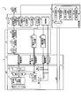
- FIG. 2 is a block diagram showing functions of main parts of the endoscope system according to Embodiment 1 of the present invention.
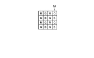
- FIG. 3 is a diagram schematically showing the configuration of the color filter according to Embodiment 1 of the present invention.
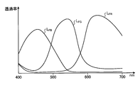
- FIG. 4 is a diagram showing the spectral sensitivity characteristics of the filters shown in FIG.
- FIG. 5 is a diagram schematically illustrating spectral characteristics of white light emitted from the white light source unit of the light source device according to Embodiment 1 of the present invention.
- FIG. 1 is a schematic diagram schematically showing an overall configuration of an endoscope system according to Embodiment 1 of the present invention.
- FIG. 2 is a block diagram showing functions of main parts of the endoscope system according to Embodiment 1 of the present invention.
- FIG. 3 is a diagram schematically showing the configuration of the color filter according to Embod
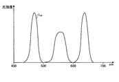
- FIG. 6 is a diagram schematically showing the spectral characteristics of two different narrow-band lights emitted from the special light source unit of the light source device according to Embodiment 1 of the present invention.
- FIG. 7 is a circuit diagram showing a detailed configuration of the first chip shown in FIG.
- FIG. 8 is a diagram showing a relationship between the intensity of the narrow band light and the output value of each pixel when the first light source unit according to Embodiment 1 of the present invention emits the narrow band light.
- FIG. 9 is a diagram showing the relationship between the intensity of special light and the output value of each pixel when the light source device according to Embodiment 1 of the present invention emits special light.
- FIG. 7 is a circuit diagram showing a detailed configuration of the first chip shown in FIG.
- FIG. 8 is a diagram showing a relationship between the intensity of the narrow band light and the output value of each pixel when the first light source unit according to Embodiment 1 of the present invention emits the narrow band light.
- FIG. 9 is
- FIG. 10 is a diagram schematically illustrating the timing at which the reading unit reads a signal from each pixel unit of the light receiving unit when the light source device according to Embodiment 1 of the present invention emits white light.
- FIG. 11 is a diagram illustrating a timing chart of an enlarged portion of the region B1 in FIG.
- FIG. 12 is a diagram schematically illustrating the timing at which the reading unit reads a signal from each pixel unit of the light receiving unit when the light source device according to Embodiment 1 of the present invention emits special light.
- FIG. 13 is a diagram showing a timing chart of an enlarged portion of the region B2 in FIG. FIG.
- FIG. 14 is a diagram schematically illustrating the timing at which the reading unit reads signals from each pixel unit of the light receiving unit when the light source device according to Embodiment 2 of the present invention emits special light.
- FIG. 15 is a diagram showing a timing chart of an enlarged portion of the region B3 in FIG.
- FIG. 16 is a block diagram illustrating functions of main parts of the endoscope system according to Embodiment 3 of the present invention.
- FIG. 17 is a diagram schematically illustrating the sensitivity ratio of each filter with respect to each light source.
- FIG. 18 is a diagram schematically showing an example of storage time information recorded by the storage time memory according to Embodiment 3 of the present invention.
- FIG. 19 is a circuit diagram showing a detailed configuration of the first chip shown in FIG.
- an endoscope system including an endoscope in which a tip is inserted into a subject will be described. Further, the present invention is not limited by this embodiment. Further, in the description of the drawings, the same portions will be described with the same reference numerals. Furthermore, the drawings are schematic, and it should be noted that the relationship between the thickness and width of each member, the ratio of each member, and the like are different from the actual ones. Moreover, the part from which a mutual dimension and ratio differ also in between drawings.
- FIG. 1 is a schematic diagram schematically showing an overall configuration of an endoscope system according to Embodiment 1 of the present invention.
- An endoscope system 1 shown in FIG. 1 includes an endoscope 2, a transmission cable 3, a connector unit 5, a processor 6 (processing device), a display device 7, and a light source device 8.
- the endoscope 2 images the inside of the subject by inserting the insertion portion 100 that is a part of the transmission cable 3 into the body cavity of the subject, and outputs an imaging signal (image data) to the processor 6.
- the endoscope 2 is provided on one end side of the transmission cable 3 and on the distal end 101 side of the insertion unit 100 that is inserted into the body cavity of the subject, an imaging unit 20 (imaging device) that captures in-vivo images.
- an operation unit 4 On the proximal end 102 side of the insertion unit 100, an operation unit 4 that receives various operations on the endoscope 2 is provided.
- the imaging signal of the image captured by the imaging unit 20 is output to the connector unit 5 through the transmission cable 3 having a length of several meters, for example.
- the transmission cable 3 connects the endoscope 2 and the connector unit 5, and connects the endoscope 2 and the light source device 8. In addition, the transmission cable 3 propagates the imaging signal generated by the imaging unit 20 to the connector unit 5.
- the transmission cable 3 is configured using a cable, an optical fiber, or the like.
- the connector unit 5 is connected to the endoscope 2, the processor 6, and the light source device 8, performs predetermined signal processing on the imaging signal output from the connected endoscope 2, and converts the analog imaging signal into a digital imaging signal. (A / D conversion) and output to the processor 6.
- the processor 6 performs predetermined image processing on the imaging signal input from the connector unit 5 and outputs the processed image signal to the display device 7.
- the processor 6 connects the entire endoscope system 1 in an integrated manner. For example, the processor 6 performs control to switch the illumination light emitted from the light source device 8 or switch the imaging mode of the endoscope 2.
- the display device 7 displays an image corresponding to the imaging signal that has been subjected to image processing by the processor 6.
- the display device 7 displays various information related to the endoscope system 1.
- the display device 7 is configured using a display panel such as liquid crystal or organic EL (Electro Luminescence).
- the light source device 8 irradiates illumination light from the distal end 101 side of the insertion portion 100 of the endoscope 2 toward the subject via the connector portion 5 and the transmission cable 3.
- the light source device 8 is configured using a white LED (Light Emitting Diode) that emits white light, an LED that emits special light of narrow band light having a wavelength band narrower than the wavelength band of white light, and the like.
- the light source device 8 irradiates the subject with white light or narrow-band light through the endoscope 2 under the control of the processor 6.
- the light source device 8 employs a simultaneous illumination method.
- FIG. 2 is a block diagram showing functions of a main part of the endoscope system 1. With reference to FIG. 2, the detail of each part structure of the endoscope system 1 and the path
- the endoscope 2 shown in FIG. 2 includes an imaging unit 20, a transmission cable 3, and a connector unit 5.
- the imaging unit 20 includes a first chip 21 (imaging element) and a second chip 22.
- the imaging unit 20 receives the power supply voltage VDD generated by the power supply voltage generation unit 55 of the connector unit 5 described later via the transmission cable 3 together with the ground GND.
- a power supply stabilizing capacitor C1 is provided between the power supply voltage VDD supplied to the imaging unit 20 and the ground GND.
- the first chip 21 is arranged in a two-dimensional matrix, receives a light from the outside, generates a light signal corresponding to the amount of received light, and outputs a plurality of unit pixels 230 and outputs the light receiving unit 23.
- a readout unit 24 that reads out an imaging signal photoelectrically converted by each of the plurality of unit pixels 230 in the light receiving unit 23, and a readout unit 24 that generates a timing signal based on the reference clock signal and the synchronization signal input from the connector unit 5.
- a color filter 26 disposed on the light receiving surface of each of the plurality of unit pixels 230.
- FIG. 3 is a diagram schematically showing the configuration of the color filter 26.
- the color filter 26 has a spectral characteristic having a maximum transmission spectrum in the red wavelength band and higher transmittance in the narrow wavelength band than in the green and blue wavelength bands.
- a red filter (hereinafter referred to as “R filter”) having a maximum transmission spectrum in the green wavelength band and a higher transmittance in the narrowband light wavelength band than the transmission spectrum in the red and blue wavelength bands
- R filter red filter
- G filter having characteristics
- each of the R filter, the G filter, the B filter, and the G filter is disposed in each unit pixel 230.
- the color filter 26 is alternately arranged in the order of the G filter and the B filter in the even lines of the light receiving unit 23, and is alternately arranged in the order of the R filter and the G filter in the odd lines of the light receiving unit 23. Is done.
- the unit pixel 230 in which the R filter is disposed on the light receiving surface is the R pixel
- the unit pixel 230 in which the G filter is disposed is the G pixel
- the unit pixel 230 in which the B filter is disposed is the B pixel. It will be described as a pixel.
- FIG. 4 is a diagram showing the spectral transmittance characteristics of the filters shown in FIG.
- the horizontal axis indicates the wavelength (nm) and the vertical axis indicates the transmittance.
- a curve L FB indicates the transmission characteristic of the B filter
- a curve L FG indicates the transmission characteristic of the G pixel
- a curve L FR indicates the transmission characteristic of the R pixel.
- the R filter has the maximum value of the transmission spectrum in the red wavelength band, and the transmittance in the wavelength band of the narrowband light described later from the transmission spectrum in the green and blue wavelength bands Has high spectral characteristics.
- the R filter has a minimum value of the transmission spectrum in the vicinity of the maximum value of the transmission spectrum of the B filter, and has a spectral characteristic in which the transmittance gradually increases toward the short wavelength side. More specifically, the R filter has spectral characteristics in which the transmittance gradually increases toward the shorter wavelength side than 440 nm. Also, as shown by the curve L FG in FIG.
- the G filter has a maximum value of the transmission spectrum in the green wavelength band, and the wavelength band of the narrowband light described later from the transmission spectrum of the red and blue wavelength bands.
- Spectral characteristics with high transmittance Specifically, the G filter has a minimum value of the transmission spectrum in the vicinity of the maximum value of the transmission spectrum of the B filter, and has a spectral characteristic in which the transmittance gradually increases toward the short wavelength side. More specifically, the R filter has spectral characteristics in which the transmittance gradually increases toward the shorter wavelength side than 440 nm.
- the B filter has the maximum value of the transmission spectrum in the blue wavelength band, and the wavelength band of the narrowband light described later from the transmission spectrum of the red and green wavelength bands.
- Spectral characteristics with high transmittance Specifically, the B filter has spectral characteristics in which the transmittance gradually decreases from the vicinity of the maximum value of the transmission spectrum toward the short wavelength side.
- the second chip 22 includes a buffer 27 that amplifies an imaging signal output from each of the plurality of unit pixels 230 in the first chip 21 and outputs the amplified image signal to the transmission cable 3.
- the combination of the circuits arranged on the first chip 21 and the second chip 22 can be changed as appropriate.
- the timing generation unit 25 arranged on the first chip 21 may be arranged on the second chip 22.
- the light guide 28 irradiates the illumination light emitted from the light source device 8 toward the subject.
- the light guide 28 is realized using a glass fiber, an illumination lens, or the like.
- the connector unit 5 includes an analog front end unit 51 (hereinafter referred to as “AFE unit 51”), an A / D conversion unit 52, an imaging signal processing unit 53, a drive pulse generation unit 54, and a power supply voltage generation unit. 55.
- the AFE unit 51 receives an imaging signal propagated from the imaging unit 20, performs impedance matching using a passive element such as a resistor, extracts an AC component using a capacitor, and determines an operating point using a voltage dividing resistor To do. Thereafter, the AFE unit 51 corrects the imaging signal (analog signal) and outputs the corrected image signal to the A / D conversion unit 52.
- a passive element such as a resistor
- the AFE unit 51 corrects the imaging signal (analog signal) and outputs the corrected image signal to the A / D conversion unit 52.
- the A / D conversion unit 52 converts the analog imaging signal input from the AFE unit 51 into a digital imaging signal and outputs the digital imaging signal to the imaging signal processing unit 53.
- the imaging signal processing unit 53 is configured by, for example, an FPGA (Field Programmable Gate Array), and performs processing such as noise removal and format conversion processing on the digital imaging signal input from the A / D conversion unit 52 to perform processing. 6 is output.
- FPGA Field Programmable Gate Array
- the drive pulse generation unit 54 is supplied from the processor 6 and is a synchronization that represents the start position of each frame based on a reference clock signal (for example, a 27 MHz clock signal) serving as a reference for the operation of each component of the endoscope 2.
- a signal is generated and output to the timing generation unit 25 of the imaging unit 20 via the transmission cable 3 together with the reference clock signal.
- the synchronization signal generated by the drive pulse generation unit 54 includes a horizontal synchronization signal and a vertical synchronization signal.
- the power supply voltage generation unit 55 generates a power supply voltage necessary for driving the first chip 21 and the second chip 22 from the power supplied from the processor 6 and outputs the power supply voltage to the first chip 21 and the second chip 22. .
- the power supply voltage generation unit 55 generates a power supply voltage necessary for driving the first chip 21 and the second chip 22 using a regulator or the like.
- the processor 6 is a control device that comprehensively controls the entire endoscope system 1.
- the processor 6 includes a power supply unit 61, an image signal processing unit 62, a clock generation unit 63, a recording unit 64, an input unit 65, and a processor control unit 66.
- the power supply unit 61 generates a power supply voltage VDD, and supplies the generated power supply voltage VDD to the power supply voltage generation unit 55 of the connector unit 5 together with the ground (GND).
- the image signal processing unit 62 performs a synchronization process, a white balance (WB) adjustment process, a gain adjustment process, a gamma correction process, a digital analog (for a digital image signal that has been subjected to signal processing by the image signal processing unit 53.
- WB white balance
- D / A Image processing such as conversion processing and format conversion processing is performed to convert it into an image signal, and this image signal is output to the display device 7.
- the clock generation unit 63 generates a reference clock signal that serves as a reference for the operation of each component of the endoscope system 1, and outputs this reference clock signal to the drive pulse generation unit 54.
- the recording unit 64 records various information related to the endoscope system 1, data being processed, and the like.
- the recording unit 64 is configured using a recording medium such as a flash memory or a RAM (Random Access Memory).
- the input unit 65 receives input of various operations related to the endoscope system 1. For example, the input unit 65 receives an input of an instruction signal for switching the type of illumination light emitted from the light source device 8.
- the input unit 65 is configured using, for example, a cross switch or a push button.
- the processor control unit 66 comprehensively controls each unit constituting the endoscope system 1.
- the processor control unit 66 is configured using a CPU (Central Processing Unit) or the like.
- the processor control unit 66 switches the illumination light emitted from the light source device 8 in accordance with the instruction signal input from the input unit 65.
- the light source device 8 includes a white light source unit 81, a special light source unit 82, a condenser lens 83, and an illumination control unit 84.
- the white light source unit 81 emits white light toward the light guide 28 via the condenser lens 83 under the control of the illumination control unit 84.
- the white light source unit 81 is configured using a white LED (Light Emitting Diode).
- the white light source unit 81 is configured with a white LED.
- a xenon lamp or a combination of a red LED, a green LED, and a blue LED may be used to emit white light.
- the special light source unit 82 simultaneously emits two narrow band lights having different wavelength bands toward the light guide 28 via the condenser lens 83 under the control of the illumination control unit 84.
- the special light source unit 82 includes a first light source unit 82a and a second light source unit 82b.
- the first light source unit 82a is configured using a purple LED.
- the first light source unit 82 a emits narrowband light having a narrower band than the blue wavelength band under the control of the illumination control unit 84.
- the first light source unit 82a emits narrowband light having a wavelength band of 390 nm to 440 nm under the control of the illumination control unit 84.
- the second light source unit 82b is configured using a green LED. Under the control of the illumination control unit 84, the second light source unit 82b emits narrowband light having a narrower band than the green wavelength band. Specifically, the second light source unit 82b emits narrowband light having a wavelength band of 530 nm to 550 nm under the control of the illumination control unit 84.
- FIG. 5 is a diagram schematically illustrating the spectral characteristics of white light emitted from the white light source unit 81.
- FIG. 6 is a diagram schematically showing the spectral characteristics of two narrowband lights having different wavelength bands emitted from the special light source unit 82. 5 and 6, the horizontal axis indicates the wavelength (nm), and the vertical axis indicates the light intensity. 5 shows the spectral characteristics of the white light curve L W is emitted by the white light source unit 81.
- a curve L NB shows the spectral characteristics of the narrowband light emitted from the first light source unit 82a
- a curve L NG shows the spectral characteristics of the narrowband light emitted by the second light source unit 82b.
- the white light source unit 81 As shown by the curve L W in FIG. 5, the white light source unit 81, a red wavelength band, a white light including each of the green wavelength band and a blue wavelength band is emitted. Further, as shown by a curve LNB in FIG. 6, the first light source unit 82a emits narrow band light having a narrow band (390 nm to 440 nm) narrower than the blue wavelength band. Further, as shown by a curve LNG in FIG. 6, the second light source unit 82b emits narrowband light having a narrow band (530 nm to 550 nm) narrower than the green wavelength band. Furthermore, as shown in FIG.
- the illumination control unit 84 includes a plurality of red filters, green filters, and blue filters. Based on the sensitivity ratio of each of the unit pixels 230, the intensity of the narrow band light emitted from the first light source unit 82a is set to be larger than the intensity of the narrow band light emitted from the second light source unit 82b. Control is performed to cause the light source unit 82a to emit narrowband light. For example, the illumination control unit 84 controls the intensity of the narrowband light emitted from the first light source unit 82a to be approximately five times the intensity of the narrowband light emitted from the second light source unit 82b.
- the condenser lens 83 condenses the white light emitted from the white light source unit 81 or the special light emitted from the special light source unit 82 and emits the condensed light to the light guide 28.
- the condenser lens 83 is configured using one or a plurality of lenses.
- the illumination control unit 84 controls the white light source unit 81 and the special light source unit 82 under the control of the processor control unit 66. Specifically, the illumination control unit 84 causes the white light source unit 81 to emit white light or the special light source unit 82 to emit narrowband light under the control of the processor control unit 66. The illumination control unit 84 controls the emission timing at which the white light source unit 81 emits white light or the emission timing at which the special light source unit 82 emits narrow band light. In the first embodiment, the illumination control unit 84 controls each of the white light source unit 81 and the special light source unit 82 by PWM control.
- the illumination control unit 84 causes the first light source unit 82a and the second light source unit 82b to simultaneously emit two narrow band lights having different wavelength bands.
- the illumination control unit 84 has each of the plurality of unit pixels 230 formed by arranging any one of a red filter, a green filter, and a blue filter. Based on the sensitivity ratio, the intensity of the narrow band light emitted from the first light source unit 82a is made larger than the intensity of the narrow band light emitted from the second light source unit 82b, and the narrow band light is transmitted to the first light source unit 82a. Is controlled to emit light.
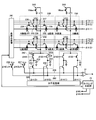
- FIG. 7 is a circuit diagram showing a configuration of the first chip 21.
- the first chip 21 shown in FIG. 7 includes at least a timing generation unit 25, an output unit 31 (amplifier), a plurality of pixels 230, a constant current source 240, a vertical scanning unit 241 (row selection circuit), a CDS.
- a (Correlated Double Sampling) unit 242, a horizontal scanning unit 243 (column selection circuit), a first horizontal reset transistor 257, and a second horizontal reset transistor 258 are included.
- the vertical scanning unit 241 and the horizontal scanning unit 243 function as the reading unit 24.
- the timing generation unit 25 generates various drive pulses based on the reference clock signal and the synchronization signal, and outputs them to each of a vertical scanning unit 241, a CDS unit 242, and a horizontal scanning unit 243 described later.
- the timing generation unit 25 functions as a control unit that controls an accumulation time for accumulating optical signal charges in each of the plurality of unit pixels 230.
- the constant current source 240 has one end connected to the ground GND, the other end connected to the vertical transfer line 239, and a gate connected to a signal line to which the reference voltage Vbias is input.
- the imaging signal and the noise signal at the time of pixel reset are transferred to the vertical transfer line 239, and each of the noise signal and the imaging signal is output to the CDS unit 242.
- the imaging signal is shared and read from the two unit pixels 230.
- the vertical transfer line 239 functions as a transfer line.
- the CDS unit 242 samples a noise signal at the time of pixel reset in each unit pixel 230, outputs the sampled noise signal to the output unit 31, and samples an imaging signal photoelectrically converted by each unit pixel 230.
- the sampled signal signal is output to the output unit 31.
- the CDS unit 242 includes a noise sampling unit 242a and a signal sampling unit 242b.
- the noise sampling unit 242a samples a noise signal at the time of pixel reset in each unit pixel 230, and outputs the sampled noise signal to the output unit 31.
- the noise sampling unit 242a includes a first sampling switch 251, a first sampling unit 252 (capacitor), and a first output switch 253.
- the first sampling switch 251 has one end connected to the vertical transfer line 239, the other end connected to one end of the first output switch 253, and a drive pulse ⁇ NS input from the timing generator 25 to the gate.
- the first sampling unit 252 has one end connected between the first sampling switch 251 and the first output switch 253, and the other end connected to the ground GND.
- the first sampling unit 252 has a unit when the drive pulse ⁇ NS is applied to the gate of the first sampling switch 251. The noise signal from the pixel 230 is sampled (held).
- the first output switch 253 has one end connected to the first sampling switch 251, the other end connected to the first horizontal transfer line 259, and a drive pulse ⁇ H ⁇ N> input from the horizontal scanning unit 243 to the gate.
- the first output switch 253 transfers the noise signal sampled by the first sampling unit 252 to the first horizontal transfer line 259 when the drive pulse ⁇ H ⁇ N> is applied to the gate.
- the signal sampling unit 242b samples the imaging signal photoelectrically converted by each unit pixel 230 and outputs the sampled signal signal to the output unit 31.
- the signal sampling unit 242b includes a second sampling switch 254, a second sampling unit 255, and a second output switch 256.
- the second sampling switch 254 has one end connected to the vertical transfer line 239, the other end connected to one end of the second output switch 256, and a drive pulse ⁇ SS input from the timing generator 25 to the gate.
- the second sampling unit 255 has one end connected between the second sampling switch 254 and the second output switch 256, and the other end connected to the ground GND.
- the second sampling unit 255 applies the drive pulse ⁇ SS to the gate of the second sampling switch 254 when the row selection pulse ⁇ X ⁇ M> and the drive pulse ⁇ T1 ⁇ M> or the drive pulse ⁇ T2 ⁇ M> are applied to the unit pixel 230.
- the imaging signal from the unit pixel 230 is sampled (held).
- the second output switch 256 has one end connected to the second sampling switch 254, the other end connected to the second horizontal transfer line 260, and a drive pulse ⁇ H ⁇ N> input from the horizontal scanning unit 243 to the gate.
- the second output switch 256 transfers the imaging signal sampled by the second sampling unit 255 to the second horizontal transfer line 260 when the drive pulse ⁇ H ⁇ N> is applied to the gate.
- the column selection signal ⁇ H ⁇ N> is applied, and the noise signal from each unit pixel 230 at the time of pixel reset in each unit pixel 230 is transferred to the first horizontal transfer line 259 via the CDS unit 242 and output.
- the horizontal scanning unit 243 applies the column selection signal ⁇ H ⁇ N> to the selected column ⁇ N> of the light receiving unit 23 based on the driving pulse ( ⁇ H) supplied from the timing generation unit 25, and each unit.
- the imaging signal photoelectrically converted by the pixel 230 is transferred to the second horizontal transfer line 260 via the CDS unit 242 and output.
- the vertical scanning unit 241 and the horizontal scanning unit 243 function as the reading unit 24.
- Each unit pixel 230 includes a photoelectric conversion element 231 (photodiode) and a photoelectric conversion element 232, a charge conversion unit 233, a transfer transistor 234 (first transfer unit) and a transfer transistor 235, and a charge conversion unit reset unit 236 ( Transistor), a pixel source follower transistor 237, and a pixel output switch 238 (signal output unit).
- a photoelectric conversion element 231 photodiode
- a photoelectric conversion element 232 includes a charge conversion unit 233, a transfer transistor 234 (first transfer unit) and a transfer transistor 235, and a charge conversion unit reset unit 236 ( Transistor), a pixel source follower transistor 237, and a pixel output switch 238 (signal output unit).
- the unit cell includes a set of one or a plurality of photoelectric conversion elements and transfer transistors, and each unit pixel 230 includes one unit cell.
- the unit pixel 230 in which each of the R filter, the G filter, and the B filter is arranged is represented as an R pixel, a G pixel, and a B pixel.
- the photoelectric conversion element 231 and the photoelectric conversion element 232 photoelectrically convert incident light into a signal charge amount corresponding to the amount of light, and accumulate it.
- the photoelectric conversion element 231 and the photoelectric conversion element 232 have a cathode side connected to one end side of the transfer transistor 234 and the transfer transistor 235, respectively, and an anode side connected to the ground GND.
- the charge conversion unit 233 includes a floating diffusion capacitor (FD), and converts charges accumulated in the photoelectric conversion element 231 and the photoelectric conversion element 232 into a voltage.
- FD floating diffusion capacitor
- the transfer transistor 234 and the transfer transistor 235 transfer charges from the photoelectric conversion element 231 and the photoelectric conversion element 232 to the charge conversion unit 233, respectively.
- Signal lines to which drive pulses (row selection pulses) ⁇ T1 and ⁇ T2 are supplied are connected to the gates of the transfer transistor 234 and the transfer transistor 235, and the charge conversion unit 233 is connected to the other end side.
- the transfer transistor 234 and the transfer transistor 235 are turned on when the drive pulses ⁇ T1 and ⁇ T2 are supplied from the vertical scanning unit 241 via the signal line, and a signal is transmitted from the photoelectric conversion element 231 and the photoelectric conversion element 232 to the charge conversion unit 233. Transfer charge.
- the charge conversion unit reset unit 236 resets the charge conversion unit 233 to a predetermined potential.
- the charge conversion unit reset unit 236 has one end connected to the power supply voltage VDD, the other end connected to the charge conversion unit 233, and a gate connected to a signal line to which a drive pulse ⁇ R is supplied.
- the drive pulse ⁇ R is supplied from the vertical scanning unit 241 via the signal line from the vertical scanning unit 241
- the charge conversion unit reset unit 236 is turned on, releases the signal charge accumulated in the charge conversion unit 233, and causes the charge conversion unit 233 to Reset to a predetermined potential.
- One end of the pixel source follower transistor 237 is connected to the power supply voltage VDD, the other end is connected to one end of the pixel output switch 238, and a signal (image signal or reset signal) that has been voltage-converted by the charge conversion unit 233 is connected to the gate. Signal) is input.
- the pixel output switch 238 outputs the signal voltage-converted by the charge conversion unit 233 to the vertical transfer line 239.
- the other end of the pixel output switch 238 is connected to the vertical transfer line 239, and a signal line to which the drive pulse ⁇ X is supplied is connected to the gate.
- the pixel output switch 238 is turned on when the drive pulse ⁇ X is supplied to the gate of the pixel output switch 238 from the vertical scanning unit 241 via the signal line, and the imaging signal or the noise signal at the time of reset is applied to the vertical transfer line 239. Forward.
- the first horizontal reset transistor 257 has one end connected to the ground GND, the other end connected to the first horizontal transfer line 259, and a drive pulse ⁇ HCLR input from the timing generator 25 to the gate.
- the first horizontal reset transistor 257 is turned on when the drive pulse ⁇ HCLR is input from the timing generation unit 25 to the gate of the first horizontal reset transistor 257, and resets the first horizontal transfer line 259.
- the second horizontal reset transistor 258 has one end connected to the ground GND, the other end connected to the second horizontal transfer line 260, and a drive pulse ⁇ HCLR input from the timing generator 25 to the gate.
- the second horizontal reset transistor 258 is turned on when the driving pulse ⁇ HCLR is input from the timing generator 25 to the gate of the second horizontal reset transistor 258, and resets the second horizontal transfer line 260.
- the output unit 31 is configured using a differential amplifier, and removes noise by taking the difference between the noise signal transferred from the first horizontal transfer line 259 and the imaging signal transferred from the second horizontal transfer line 260. Output the imaging signal to the outside.
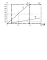
- FIG. 8 is a diagram illustrating a relationship between the intensity of the narrow band light and the output value of each pixel when the first light source unit 82a emits the narrow band light.
- the horizontal axis indicates the intensity of narrowband light emitted by the first light source unit 82a
- the vertical axis indicates the output value of each pixel.
- a curve L1 indicates an output value (pixel value) of the B pixel
- a straight line L2 indicates an output value (pixel value) of the R pixel or G pixel.
- each of the R pixel and the G pixel has low sensitivity to the narrow band region (B light), so that the intensity of the narrow band light emitted from the first light source unit 82a can be increased. Conceivable. However, as indicated by the curves L1 and L2 in the region G2, when the intensity of the narrow band light emitted from the first light source unit 82a is increased, the output value of the B pixel is saturated.
- the illumination control unit 84 increases the S / N ratio of each of the R pixel and the G pixel by increasing the intensity of the narrowband light emitted from the first light source unit 82a. Further, in the first embodiment, the timing generation unit 25 shortens the accumulation time for accumulating the optical signal charge in the B pixel so that the signal value of the B pixel is not saturated, so that the narrowband light by the light source device 8 is reduced. At the time of emission, the output values of the R pixel, G pixel, and B pixel can be used as image signals. Specifically, as illustrated in FIG.
- the timing generation unit 25 artificially shortens the accumulation time for accumulating light in the B pixel so that the signal value of the B pixel does not saturate, thereby artificially creating the R pixel or G pixel.
- the output values of the R, G, and B pixels can be used as image signals when the light source device 8 emits narrowband light. To do. In this case, it is desirable that the color filter 26 has the spectral characteristics shown in FIG.
- FIG. 10 is a diagram schematically illustrating the timing at which the reading unit 24 reads a signal from each unit pixel 230 of the light receiving unit 23 when the light source device 8 emits white light.
- FIG. 11 is a diagram illustrating a timing chart of an enlarged portion of the region B1 in FIG. In FIG.
- the reading unit 24 reads out the imaging signal from each unit pixel 230 for each horizontal line based on each drive pulse input from the timing generation unit 25, and The data is output to the buffer 27 of the 2-chip 22.
- the timing generation unit 25 sets the row selection pulse ⁇ X ⁇ 0> to an on state (High).
- the timing generation unit 25 sets the drive pulse ⁇ R ⁇ 0> to the on state (High).
- the charge conversion unit reset unit 236 resets the charge conversion unit 233 to a predetermined potential.
- the timing generation unit 25 sets the drive pulse ⁇ R ⁇ 0> to the off state (Low) and sets the drive pulse ⁇ NS to the on state (High).
- the noise signal of the charge conversion unit 233 is sampled by the first sampling unit 252 via the vertical transfer line 239.
- the timing generation unit 25 sets the drive pulse ⁇ T1 ⁇ 0> to an on state (High) and sets the drive pulse ⁇ SS to an on state (High).
- the transfer transistor 234 is turned on when the drive pulse ⁇ T1 ⁇ 0> is supplied from the timing generation unit 25 to the gate, and transfers the signal charge from the photoelectric conversion element 231 to the charge conversion unit 233.
- the pixel output switch 238 outputs the imaging signal voltage-converted by the charge conversion unit 233 from the pixel source follower transistor 237 to the vertical transfer line 239.
- the second sampling unit 255 samples the imaging signal output from the vertical transfer line 239.
- the timing generation unit 25 sets the row selection pulse ⁇ X ⁇ 0> to the OFF state (Low) after setting the drive pulse ⁇ SS to the OFF state (Low), and applies the column selection pulse ⁇ H ⁇ N> to each column.
- the on / off operation is sequentially repeated.
- each second sampling unit 255 transfers the sampled G pixel imaging signal to the second horizontal transfer line 260 and outputs it to the output unit 31. Thereby, the imaging signal of each G pixel is output.
- the timing generation unit 25 sets the row selection pulse ⁇ X ⁇ 0> to the on state (High).
- the timing generation unit 25 sets the drive pulse ⁇ R ⁇ 0> to the on state (High).
- the charge conversion unit reset unit 236 is turned on when the drive pulse ⁇ R ⁇ 0> is input from the timing generation unit 25 to the gate, and resets the charge conversion unit 233 to a predetermined potential.
- the timing generation unit 25 sets the drive pulse ⁇ R ⁇ 0> to the off state (Low) and sets the drive pulse ⁇ NS to the on state (High).
- the noise signal of the charge conversion unit 233 is sampled by the first sampling unit 252 via the vertical transfer line 239.
- the timing generation unit 25 sets the drive pulse ⁇ T2 ⁇ 0> to the on state (High) and sets the drive pulse ⁇ SS to the on state (High).
- the transfer transistor 235 is turned on when the drive pulse ⁇ T2 ⁇ 0> is supplied from the timing generation unit 25 to the gate, and transfers the signal charge from the photoelectric conversion element 232 to the charge conversion unit 233.
- the pixel output switch 238 outputs the imaging signal voltage-converted by the charge conversion unit 233 from the pixel source follower transistor 237 to the vertical transfer line 239.
- the second sampling unit 255 samples the imaging signal output from the vertical transfer line 239.
- the timing generation unit 25 sets the row selection pulse ⁇ X ⁇ 0> to the OFF state (Low) after setting the drive pulse ⁇ SS to the OFF state (Low), and applies the column selection pulse ⁇ H ⁇ N> to each column.
- the on / off operation is sequentially repeated.
- each second sampling unit 255 transfers the sampled B pixel imaging signal to the second horizontal transfer line 260 and outputs it to the output unit 31. Thereby, the imaging signal of each B pixel is output.
- the readout unit 24 reads out the imaging signal from each unit pixel 230 for each unit pixel 230 for each horizontal line, and outputs it to the buffer 27 of the second chip 22.
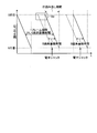
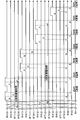
- FIG. 12 is a diagram schematically illustrating the timing at which the reading unit 24 reads a signal from each unit pixel 230 of the light receiving unit 23 when the light source device 8 emits narrowband light.
- FIG. 13 is a diagram showing a timing chart of an enlarged portion of the region B2 in FIG.
- the timing generation unit 25 controls the timing of outputting each drive pulse according to the sensitivity to the narrowband light (B light) emitted from the first light source unit 82a.
- the accumulation time of each of the G pixel and the R pixel and the accumulation time of the B pixel are adjusted.
- the timing generation unit 25 controls the accumulation time of the B pixel with the electronic shutter so that it becomes approximately 1/5 of the accumulation time of each of the G pixel and the R pixel.
- the timing generator 25 turns on each of the drive pulse ⁇ R ⁇ 0> and the drive pulse ⁇ T2 ⁇ 0>. Thereby, the signal charge accumulated in the photoelectric conversion element 232 corresponding to the B pixel is released to the power supply voltage VDD. As a result, the signal charge accumulated in the photoelectric conversion element 231 corresponding to the B pixel is reset. As described above, the timing generation unit 25 controls the accumulation time of the B pixel with the electronic shutter so as to be approximately 1/5 of the accumulation time of each of the G pixel and the R pixel.
- the timing generation unit 25 turns off each of the drive pulse ⁇ R ⁇ 0> and the drive pulse ⁇ T2 ⁇ 0>, and performs signal charge accumulation in the B pixel.
- the timing generation unit 25 After accumulating the signal charges of the B pixel, the timing generation unit 25 sets the row selection pulse ⁇ X ⁇ 0> to the on state (High) and the drive pulse ⁇ R to the on state (High). As a result, the charge conversion unit reset unit 236 is turned on, releases the signal charge accumulated in the charge conversion unit 233, and resets the charge conversion unit 233 to a predetermined potential. Subsequently, the timing generation unit 25 turns on the drive pulse ⁇ NS, and causes the first sampling unit 252 to sample the noise signal input from the charge conversion unit 233 via the vertical transfer line 239.
- the timing generation unit 25 sets the drive pulse ⁇ NS to the off state (Low). Thereby, the first sampling unit 252 completes sampling of the noise signal.
- the timing generation unit 25 sets the drive pulse ⁇ T1 ⁇ 0> to an on state (High) and sets the drive pulse ⁇ SS to an on state (High).
- the transfer transistor 234 is turned on when the drive pulse ⁇ T1 ⁇ 0> is supplied from the timing generation unit 25 to the gate, and transfers the signal charge from the photoelectric conversion element 231 to the charge conversion unit 233.
- the pixel output switch 238 outputs the imaging signal voltage-converted by the charge conversion unit 233 from the pixel source follower transistor 237 to the vertical transfer line 239.
- the second sampling unit 255 samples the imaging signal output from the vertical transfer line 239.
- the timing generation unit 25 sets the row selection pulse ⁇ X ⁇ 0> to the OFF state (Low) after setting the drive pulse ⁇ SS to the OFF state (Low), and applies the column selection pulse ⁇ H ⁇ N> to each column.
- the on / off operation is sequentially repeated.
- each second sampling unit 255 transfers the sampled G pixel imaging signal to the second horizontal transfer line 260 and outputs it to the output unit 31.
- Each first sampling unit 252 outputs the sampled noise signal to the first horizontal transfer line 260. Transfer to one horizontal transfer line 259 and output to output unit 31.
- the output unit 31 outputs the difference between the imaging signal of each G pixel and the noise signal, and thereby outputs the imaging signal of each G pixel from which noise has been removed.
- the timing generation unit 25 sets the row selection pulse ⁇ X ⁇ 0> to the on state (High).
- the timing generation unit 25 sets the drive pulse ⁇ R ⁇ 0> to the on state (High).
- the charge conversion unit reset unit 236 is turned on when the drive pulse ⁇ R ⁇ 0> is input from the timing generation unit 25 to the gate, and resets the charge conversion unit 233 to a predetermined potential.
- the timing generation unit 25 sets the drive pulse ⁇ R ⁇ 0> to the off state (Low) and sets the drive pulse ⁇ NS to the on state (High).
- the first sampling switch 251 is turned on, and causes the first sampling unit 252 to sample the noise signal input from the charge conversion unit 233 via the vertical transfer line 239.
- the timing generation unit 25 sets the drive pulse ⁇ NS to the off state (Low). Thereby, the first sampling unit 252 completes sampling of the noise signal.
- the timing generation unit 25 sets the drive pulse ⁇ T2 ⁇ 0> to the on state (High) and sets the drive pulse ⁇ SS to the on state (High).
- the transfer transistor 235 is turned on when the drive pulse ⁇ T2 ⁇ 0> is supplied from the timing generation unit 25 to the gate, and transfers the signal charge from the photoelectric conversion element 232 to the charge conversion unit 233.
- the pixel output switch 238 outputs the imaging signal voltage-converted by the charge conversion unit 233 from the pixel source follower transistor 237 to the vertical transfer line 239.
- the second sampling unit 255 samples the imaging signal output from the vertical transfer line 239.
- the timing generation unit 25 sets the row selection pulse ⁇ X ⁇ 0> to the OFF state (Low) after setting the drive pulse ⁇ SS to the OFF state (Low), and applies the column selection pulse ⁇ H ⁇ N> to each column.
- the on / off operation is sequentially repeated.
- each second sampling unit 255 transfers the sampled B pixel imaging signal to the second horizontal transfer line 260 and outputs it to the output unit 31.
- an image pickup signal for each B pixel whose accumulation time is approximately 1/5 of the accumulation time for each of the G and R pixels, is output.
- the timing generation unit 25 adjusts the accumulation time of the B pixel so that the accumulation time of the B pixel becomes approximately 1/5 of the accumulation time of each of the G pixel and the R pixel by performing the electronic shutter.
- the accumulation time is controlled so as not to saturate.
- the R filter has the maximum value of the transmission spectrum in the red wavelength band, and the transmittance in the wavelength band of the narrow band light than the transmission spectrum of the green and blue wavelength bands.
- the G filter has the maximum value of the transmission spectrum in the green wavelength band, and the spectral characteristic has a higher transmittance in the narrow wavelength band than the transmission spectrum in the red and blue wavelength bands.
- the B filter has a maximum transmission spectrum value in the blue wavelength band, and has a spectral characteristic in which the transmittance in the wavelength band of narrowband light is higher than the transmission spectrum in the red and green wavelength bands, and the timing generator 25 Since the storage time for storing the optical signal charge in each unit pixel 230 is individually controlled, an image with high resolution can be obtained regardless of whether narrow-band light or white light is irradiated. It can be.
- the first light source unit 82a emits the plurality of unit pixels 230 in which the timing generation unit 25 arranges any one of the red filter, the green filter, and the blue filter. Since the control is performed so that the accumulation time of the B pixel having the highest spectral sensitivity with respect to the narrow band light is shorter than the accumulation time of the unit pixel 230 in which the R filter or the G filter is arranged, the narrow light emitted from the first light source unit 82a is controlled. Even when the intensity of the band light is higher than the intensity of the narrow band light emitted from the second light source unit 82b, the B pixel can be prevented from being saturated.
- the red filter has a spectral characteristic that the transmission spectrum gradually increases toward the shorter wavelength side from 440 nm, and the green filter has the transmission spectrum toward the shorter wavelength side from 440 nm. Therefore, even when white light is irradiated on the subject, color reproducibility is good and color noise can be prevented from occurring.
- the illumination control unit 84 controls the intensity of the narrowband light emitted from the first light source unit 82a based on the sensitivity ratio of each of the R pixel, the G pixel, and the B pixel. Therefore, when the endoscope system 1 performs the NBI observation mode, an image with high resolution can be obtained.
- the endoscope system according to the second embodiment has the same configuration as that of the first embodiment described above, and the readout timing of the readout unit by the timing generation unit is different.
- the timing generation unit 25 according to the first embodiment described above controls the accumulation time so that the B pixel is not saturated by performing an electronic shutter operation in each row.
- the timing generation unit according to (1) controls the accumulation time so that the B pixel is not saturated by simultaneously performing the shutter operation (global shutter) on all rows.
- the readout timing for each pixel by the timing generation unit according to the second embodiment will be described.
- symbol is attached
- FIG. 14 is a diagram schematically illustrating the timing at which the reading unit 24 reads a signal from each unit pixel 230 of the light receiving unit 23 when the light source device 8 according to Embodiment 2 of the present invention emits narrowband light. is there.
- FIG. 15 is a diagram showing a timing chart of an enlarged portion of the region B3 in FIG.
- the timing generation unit 25 controls the timing of outputting each drive pulse in accordance with the sensitivity to the narrowband light (B light) emitted from the first light source unit 82 a, so that the G pixel and The accumulation time of each R pixel and the accumulation time of the B pixel are adjusted. Specifically, the timing generation unit 25 controls the accumulation time of the B pixel with the global shutter so that it becomes approximately 1/5 of the accumulation time of each of the G pixel and the R pixel. Furthermore, the illumination control unit 84 emits narrowband light in addition to the row readout period in which the readout unit 24 reads the imaging signal from the light receiving unit 23 by performing PWM control (narrowband light emission period).
- the timing generation unit 25 performs driving pulses ⁇ R ⁇ 0, 2, 4,..., M> for even lines and driving pulses ⁇ T2 ⁇ 0, 2, 4,. ..M-2 and m> are simultaneously turned on. Thereby, the signal charge accumulated in the photoelectric conversion element 231 corresponding to the B pixel is released to the power supply voltage VDD. As a result, the signal charge accumulated in the photoelectric conversion element 231 corresponding to the B pixel is reset. As described above, the timing generation unit 25 controls the accumulation time of the B pixel by the global shutter (electronic shutter) so that it becomes approximately 1/5 of the accumulation time of each of the G pixel and the R pixel.
- the global shutter electronic shutter
- the timing generation unit 25 turns off each of the drive pulses ⁇ R ⁇ 0, 2, 4,..., M> and each of the drive pulses ⁇ T2 ⁇ 0, 2, 4,. , B signal accumulation is performed.
- the timing generation unit 25 After accumulating the signal charges of the B pixel, the timing generation unit 25 sets the row selection pulse ⁇ X ⁇ 0> to the on state (High) and the drive pulse ⁇ R to the on state (High). As a result, the charge conversion unit reset unit 236 is turned on, releases the signal charge accumulated in the charge conversion unit 233, and resets the charge conversion unit 233 to a predetermined potential. Subsequently, the timing generation unit 25 turns on the drive pulse ⁇ NS, and causes the first sampling unit 252 to sample the noise signal input from the charge conversion unit 233 via the vertical transfer line 239.
- the timing generation unit 25 sets the drive pulse ⁇ NS to the off state (Low). Thereby, the first sampling unit 252 completes sampling of the noise signal.
- the timing generation unit 25 sets the drive pulse ⁇ T1 ⁇ 0> to an on state (High) and sets the drive pulse ⁇ SS to an on state (High).
- the transfer transistor 234 is turned on when the drive pulse ⁇ T1 ⁇ 0> is supplied from the timing generation unit 25 to the gate, and transfers the signal charge from the photoelectric conversion element 231 to the charge conversion unit 233.
- the pixel output switch 238 outputs the imaging signal voltage-converted by the charge conversion unit 233 from the pixel source follower transistor 237 to the vertical transfer line 239.
- the second sampling unit 255 samples the imaging signal output from the vertical transfer line 239.
- the timing generation unit 25 sets the row selection pulse ⁇ X ⁇ 0> to the OFF state (Low) after setting the drive pulse ⁇ SS to the OFF state (Low), and applies the column selection pulse ⁇ H ⁇ N> to each column.
- the on / off operation is sequentially repeated.
- each second sampling unit 255 transfers the sampled G pixel imaging signal to the second horizontal transfer line 260 and outputs it to the output unit 31.
- Each first sampling unit 252 outputs the sampled noise signal to the first horizontal transfer line 260. Transfer to one horizontal transfer line 259 and output to output unit 31.
- the output unit 31 outputs the difference between the imaging signal of each G pixel and the noise signal, and thereby outputs the imaging signal of each G pixel from which noise has been removed.
- the timing generation unit 25 sets the row selection pulse ⁇ X ⁇ 0> to the on state (High).
- the timing generation unit 25 sets the drive pulse ⁇ R ⁇ 0> to the on state (High).
- the charge conversion unit reset unit 236 is turned on when the drive pulse ⁇ R ⁇ 0> is input from the timing generation unit 25 to the gate, and resets the charge conversion unit 233 to a predetermined potential.
- the timing generation unit 25 sets the drive pulse ⁇ R ⁇ 0> to the off state (Low) and sets the drive pulse ⁇ NS to the on state (High).
- the charge conversion unit reset unit 236 is turned on, releases the signal charge accumulated in the charge conversion unit 233, and resets the charge conversion unit 233 to a predetermined potential.
- the first sampling switch 251 is turned on, and causes the first sampling unit 252 to sample the noise signal input from the charge conversion unit 233 via the vertical transfer line 239.
- the timing generation unit 25 sets the drive pulse ⁇ NS to the off state (Low). Thereby, sampling of the noise signal is completed.
- the timing generation unit 25 sets the drive pulse ⁇ T2 ⁇ 0> to the on state (High) and sets the drive pulse ⁇ SS to the on state (High).
- the transfer transistor 235 is turned on when the drive pulse ⁇ T2 ⁇ 0> is supplied from the timing generation unit 25 to the gate, and transfers the signal charge from the photoelectric conversion element 232 to the charge conversion unit 233.
- the pixel output switch 238 outputs the imaging signal voltage-converted by the charge conversion unit 233 from the pixel source follower transistor 237 to the vertical transfer line 239.
- the second sampling unit 255 samples the imaging signal output from the vertical transfer line 239.
- the timing generation unit 25 sets the row selection pulse ⁇ X ⁇ 0> to the OFF state (Low) after setting the drive pulse ⁇ SS to the OFF state (Low), and applies the column selection pulse ⁇ H ⁇ N> to each column.
- the on / off operation is sequentially repeated.
- each second sampling unit 255 transfers the sampled B pixel imaging signal to the second horizontal transfer line 260 and outputs it to the output unit 31.
- an image pickup signal for each B pixel whose accumulation time is approximately 1/5 of the accumulation time for each of the G and R pixels, is output.
- the timing generation unit 25 adjusts the accumulation time for accumulating the optical signal charge in the B pixel so as to be approximately 1/5 of the accumulation time of each of the G pixel and the R pixel by performing the global shutter operation.
- the accumulation time exposure time
- the B pixel is not saturated.
- Embodiment 2 of the present invention the same effect as that of Embodiment 1 described above is obtained, and an image with high resolution can be obtained regardless of whether narrowband light or white light is irradiated. Obtainable.
- the timing generation unit 25 performs control to make the accumulation time of the B pixel shorter than the accumulation time of each of the R pixel and the G pixel by the global shutter. (Rolling shutter phenomenon) can be reliably prevented.
- the endoscope system according to the third embodiment has a configuration different from that of the first embodiment described above, and controls the accumulation time according to the sensitivity ratio of each filter provided in each pixel.
- the readout timing of each pixel unit of the endoscope system according to the third embodiment will be described.
- symbol is attached
- FIG. 16 is a block diagram illustrating functions of main parts of the endoscope system according to the third embodiment.
- An endoscope system 1a shown in FIG. 16 includes an endoscope 2a instead of the endoscope 2 of the endoscope system 1 according to the first embodiment described above.
- the endoscope 2a includes an imaging unit 20a, a transmission cable 3, and a connector unit 5a.
- the connector unit 5a includes an AFE unit 51, an A / D conversion unit 52, an imaging signal processing unit 53, a power pulse generation unit 54a, a power supply voltage generation unit 55, and an accumulation time memory 56.
- the power pulse generator 54a generates a synchronization signal representing the start position of each frame based on a reference clock signal supplied from the processor 6 and serving as a reference for the operation of each component of the endoscope 2a. Along with the signal, the signal is output to the timing generator 25 of the imaging unit 20 via the transmission cable 3. Further, the power pulse generation unit 54a applies drive timing to the first chip 21a (imaging device) in the imaging unit 20a based on type information (light source information) indicating the type of light source of the light source device 8 input from the processor 6. A drive timing change signal for instructing the change is output to the timing generation unit 25 of the first chip 21a.
- the synchronization signal generated by the drive pulse generation unit 54 includes a horizontal synchronization signal and a vertical synchronization signal.
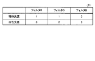
- the storage time memory 56 stores the storage time for each light source corresponding to the sensitivity ratio (transmittance) of each of the R filter, G filter, and B filter in the color filter 26 arranged on the light receiving surface of each of the plurality of unit pixels 230. Record. For example, as shown in the table T1 showing the sensitivity ratio of each filter for each light source shown in FIG. 17, the sensitivity of the R filter and the G filter for the special light source is lower than the sensitivity of the B filter, and the R filter for the white light source and The sensitivity of the G filter is almost the same.
- the accumulation time memory 56 records a table T2 indicating accumulation time information related to the accumulation time set by the reciprocal of the sensitivity ratio of each filter for each light source.
- the imaging unit 20a includes a first chip 21a and a second chip 22.
- the first chip 21a includes a light receiving unit 23, a reading unit 24a, a timing generation unit 25, and a color filter 26. The detailed configuration of the first chip 21a will be described later.
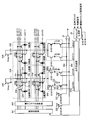
- FIG. 19 is a circuit diagram showing a configuration of the first chip 21a.
- the 19 includes at least a timing generation unit 25, an output unit 31 (amplifier), a plurality of pixels 230, a constant current source 240, a vertical scanning unit 241 (row selection circuit), a CDS. 242, a horizontal scanning unit 243 (column selection circuit), an electronic shutter scanning unit 244, a first horizontal reset transistor 257, and a second horizontal reset transistor 258.
- the vertical scanning unit 241, the horizontal scanning unit 243, and the electronic shutter scanning unit 244 function as the reading unit 24.
- the timing generation unit 25a generates various drive pulses based on the reference clock signal, the synchronization signal, and the drive timing change signal, and each of the vertical scanning unit 241, the electronic shutter scanning unit 244, the CDS unit 242, and the horizontal scanning unit 243. Output to.
- the timing generation unit 25a functions as a control unit that controls the accumulation time in which the optical signal charges are accumulated in each of the plurality of unit pixels 230 according to the sensitivity of each filter.
- the vertical scanning unit 241 and the electronic shutter scanning unit 244 drive the unit pixels 230 in different rows based on driving pulses ( ⁇ X, ⁇ R, ⁇ T1, ⁇ T2, etc.) input from the timing generation unit 25.
- the electronic shutter scanning unit 244 selectively applies each of ⁇ R and ⁇ T1 ⁇ M> or ⁇ T2 ⁇ M> to the unit pixel 230 on which a color filter for reducing the accumulation time of each unit pixel 230 to suppress saturation is mounted. Then, the signal charge (imaging signal) is discharged to the power supply voltage VDD.
- the electronic shutter scanning unit 244 can arbitrarily set the accumulation time of the unit pixels 230 corresponding to all the color filters by selecting a plurality of rows at the same time.
- the first chip 21a configured as described above has different rows based on drive pulses ( ⁇ X, ⁇ R, ⁇ T1, ⁇ T2, etc.) input from the timing generation unit 25 to the vertical scanning unit 241 and the electronic shutter scanning unit 244.
- the unit pixel 230 is driven, and the electronic shutter scanning unit 244 selectively selects ⁇ R and ⁇ T1 ⁇ M> or ⁇ T2 for the unit pixel 230 on which a color filter for which the accumulation time of each unit pixel 230 is shortened to suppress saturation is mounted.
- the signal charge (imaging signal) is discharged to the power supply voltage VDD.
- the unit pixel 230 in which the same color filter is arranged is selected from the unit pixels 230 in the row selected by the electronic shutter scanning unit 244, and the same pixel reset signal ( ⁇ R) as that in the vertical scanning unit 241 is applied.
- the accumulation time of the optical signal charge accumulated in the unit pixel 230 is controlled.
- Embodiment 3 of the present invention described above the same effect as that of Embodiment 1 described above is obtained, and an image with high resolution can be obtained regardless of whether narrowband light or white light is irradiated. Obtainable.
- the timing generation unit 25 controls the electronic shutter scanning unit 244 and the vertical scanning unit 241, so that the unit pixel is determined according to the accumulation time for each light source according to the sensitivity ratio of each filter. Since the accumulation time of 230 is controlled, all unit pixels 230 can be output at an appropriate signal level without being saturated.
- the timing generation unit controls only the accumulation time for accumulating the optical signal charge in the B pixel.
- the timing generation unit accumulates the optical signal charge in the R pixel for narrowband light.
- the accumulation time may be shorter than the accumulation time for accumulating optical signal charges in the G pixel.
- the timing generation unit may make the accumulation time of the R pixel shorter than the accumulation time of the G pixel based on the sensitivity ratio of the R pixel and the G pixel to narrowband light.
- the timing generation unit makes the accumulation time of the B pixel shorter than the accumulation time of the R pixel and the accumulation time of the R pixel based on the sensitivity of each of the B pixel, the R pixel, and the G pixel with respect to the narrowband light. It may be shorter than the B pixel accumulation time (B pixel accumulation time ⁇ R pixel accumulation time ⁇ G pixel accumulation time).
- the special light source unit emits narrow band light included in the blue wavelength band.
- the special light source unit emits narrow band light included in the infrared or near infrared wavelength band. It may be emitted.
- a Bayer array color filter using an R filter, a G filter, and a B filter is used as the color filter.
- R filter cyan, magenta, and yellow are used.
- a color filter composed of complementary color filters may be used.
- the endoscope is inserted into the subject.
- a capsule endoscope or an imaging device that images the subject can also be applied.
- the present invention can include various embodiments not described herein, and various design changes and the like can be made within the scope of the technical idea specified by the claims. Is possible.
Landscapes
- Life Sciences & Earth Sciences (AREA)
- Health & Medical Sciences (AREA)
- Surgery (AREA)
- Engineering & Computer Science (AREA)
- Biophysics (AREA)
- Medical Informatics (AREA)
- Nuclear Medicine, Radiotherapy & Molecular Imaging (AREA)
- Optics & Photonics (AREA)
- Pathology (AREA)
- Radiology & Medical Imaging (AREA)
- Veterinary Medicine (AREA)
- Biomedical Technology (AREA)
- Heart & Thoracic Surgery (AREA)
- Physics & Mathematics (AREA)
- Molecular Biology (AREA)
- Animal Behavior & Ethology (AREA)
- General Health & Medical Sciences (AREA)
- Public Health (AREA)
- Signal Processing (AREA)
- Multimedia (AREA)
- Endoscopes (AREA)
- Instruments For Viewing The Inside Of Hollow Bodies (AREA)
- Closed-Circuit Television Systems (AREA)
Abstract
狭帯域光および白色光のいずれかを照射する場合であっても、解像度が高い画像を得ることができる撮像装置、内視鏡および内視鏡システムを提供する。撮像装置は、緑色および青色の各々の波長帯域の透過スペクトルより狭帯域光の波長帯域の透過スペクトルが高い分光特性を有する赤色フィルタと、赤色および青色の各々の波長帯域の透過スペクトルより狭帯域光の波長帯域の透過スペクトルが高い分光特性を有する緑色フィルタと、赤色および緑色の各々の波長帯域の透過スペクトルより狭帯域光の波長帯域の透過スペクトルが高い分光特性を有する青色フィルタと、を含むフィルタユニットを、複数の単位画素230に対応させて配置してなるカラーフィルタ26と、複数の単位画素230の各々に光信号電荷を蓄積させる蓄積させる蓄積時間を制御するタイミング生成部25と、を備える。
Description
本発明は、被写体を撮像して該被写体の画像データを生成する撮像装置、内視鏡および内視鏡システムに関する。
近年、内視鏡システムにおいて、白色光源が発する光の波長帯域より狭く、青色と緑色の波長帯域にそれぞれ含まれる狭帯域の光(以下、「狭帯域光」という)を被検体の観察部位に照射し、この観察部位で反射した反射光を画像化して粘膜表層の毛細血管および粘膜微細模様を強調表示する技術が知られている(特許文献1参照)。この技術では、赤色(R)、緑色(G)および青色(B)をそれぞれ透過する3種類のフィルタを所定のパターンで配置したカラーフィルタが受光面上に設けられた撮像素子において、緑色の成分を透過するフィルタ(Gフィルタ)の特性として、緑色光に感応する主感度領域に加えて、青色の狭帯域光に感応する副感度領域を設けている。
特許文献1の技術では、Gフィルタを透過した光を受光する画素(G画素)の画素値、および赤色の成分を透過するフィルタ(Rフィルタ)を透過した光を受光する画素(R画素)の画素値の相関演算を行うことによって、G画素の画素値から副感度領域の画素値を抽出し、抽出した副感度領域の画素値および副感度領域の成分および青色の成分を透過するフィルタ(Bフィルタ)を透過した光を受光する画素(B画素)の画素値に基づいて、粘膜表層の毛細血管および粘膜微細模様等を強調した強調画像を表示モニタに表示させる。
しかしながら、上述した特許文献1では、R画素が青色の狭帯域光に対する感度が低いため、R画素からの画素値も小さくなることによって、解像感が低い画像となるという問題点があった。
本発明は、上記に鑑みてなされたものであって、狭帯域光および白色光のいずれを照射する場合であっても、解像度が高い画像を得ることができる撮像装置、内視鏡および内視鏡システムを提供することを目的とする。
上述した課題を解決し、目的を達成するために、本発明に係る撮像装置は、赤色の波長帯域、緑色の波長帯域および青色の波長帯域の各々を有する白色光または該白色光の波長帯域より狭い狭帯域の狭帯域光が照射された被写体を撮像して画像データを生成する撮像装置であって、二次元マトリクス状に配置され、外部から光を受光し、受光量に応じた撮像信号を生成する複数の画素と、前記赤色の波長帯域に透過スペクトルの最大値を有し、前記緑色および前記青色の波長帯域の透過スペクトルより前記狭帯域光の波長帯域の透過率が高い分光特性を有する赤色フィルタ、前記緑色の波長帯域に透過スペクトルの最大値を有し、前記赤色および前記青色の波長帯域の透過スペクトルより前記狭帯域光の波長帯域の透過率が高い分光特性を有する緑色フィルタ、および前記青色の波長帯域に透過スペクトルの最大値を有し、前記赤色および前記緑色の波長帯域の透過スペクトルより前記狭帯域光の波長帯域の透過率が高い分光特性を有する青色フィルタの各々を、前記複数の画素に対応させて配置してなるカラーフィルタと、前記複数の画素の各々に光信号電荷を蓄積させる蓄積時間を個別に制御する制御部と、を備えたことを特徴とする。
また、本発明に係る撮像装置は、上記発明において、前記制御部は、当該撮像装置が前記狭帯域光を照射された前記被写体を撮像する場合、前記複数の画素の各々の分光感度比に基づいて、前記複数の画素の各々の前記蓄積時間を個別に制御することを特徴とする。
また、本発明に係る撮像装置は、上記発明において、前記制御部は、前記複数の画素のうち前記狭帯域光に対する分光感度が最も高い画素の蓄積時間を、他のフィルタが配置されてなる画素の蓄積時間より短くする制御を行うことを特徴とする。
また、本発明に係る撮像装置は、上記発明において、前記狭帯域は、390nm~440nmであり、前記制御部は、前記青色フィルタを配置してなる画素の蓄積時間を、前記赤色フィルタおよび前記緑色フィルタを配置してなる画素の蓄積時間より短くする制御を行うことを特徴とする。
また、本発明に係る撮像装置は、上記発明において、前記赤色フィルタおよび前記緑色フィルタは、440nmより短波長側に向けて透過スペクトルが徐々に高くなる分光特性を有することを特徴とする。
また、本発明に係る撮像装置は、上記発明において、前記制御部は、電子シャッタによって前記青色フィルタを配置してなる画素の蓄積時間を制御することを特徴とする。
また、本発明に係る撮像装置は、上記発明において、前記複数の画素の各々から前記撮像信号を転送する転送ゲートをさらに備え、前記制御部は、前記青色フィルタを配置してなる画素が光を受光する蓄積期間に、前記青色フィルタを配置してなる画素の転送ゲートへシャッタパルスを出力することによって、前記電子シャッタを行うことを特徴とする。
また、本発明に係る内視鏡は、上記の撮像装置と、被検体内に挿入可能な挿入部の先端側に備えたことを特徴とする。
また、本発明に係る内視鏡システムは、上記の内視鏡と、前記狭帯域光を照射する光源部と、前記複数のフィルタのいずれか一つを配置してなる前記複数の画素の各々の感度比に基づいて、前記狭帯域光の強度を制御して前記光源部に前記狭帯域光を照射させる照明制御部と、を備えたことを特徴とする。
本発明によれば、狭帯域光および白色光のいずれかを照射する場合であっても、解像度が高い画像を得ることができるという効果を奏する。
以下、本発明を実施するための形態(以下、「実施の形態」という)として、被検体内に先端が挿入される内視鏡を備えた内視鏡システムについて説明する。また、この実施の形態により、本発明が限定されるものではない。さらに、図面の記載において、同一の部分には同一の符号を付して説明する。さらにまた、図面は、模式的なものであり、各部材の厚みと幅との関係、各部材の比率等は、現実と異なることに留意する必要がある。また、図面の相互間においても、互いの寸法や比率が異なる部分が含まれている。
〔内視鏡システムの構成〕
図1は、本発明の実施の形態1に係る内視鏡システムの全体構成を模式的に示す概略図である。図1に示す内視鏡システム1は、内視鏡2と、伝送ケーブル3と、コネクタ部5と、プロセッサ6(処理装置)と、表示装置7と、光源装置8と、を備える。
図1は、本発明の実施の形態1に係る内視鏡システムの全体構成を模式的に示す概略図である。図1に示す内視鏡システム1は、内視鏡2と、伝送ケーブル3と、コネクタ部5と、プロセッサ6(処理装置)と、表示装置7と、光源装置8と、を備える。
内視鏡2は、伝送ケーブル3の一部である挿入部100を被検体の体腔内に挿入することによって被検体の体内を撮像して撮像信号(画像データ)をプロセッサ6へ出力する。また、内視鏡2は、伝送ケーブル3の一端側であり、被検体の体腔内に挿入される挿入部100の先端101側に、体内画像の撮像を行う撮像部20(撮像装置)が設けられており、挿入部100の基端102側に、内視鏡2に対する各種操作を受け付ける操作部4が設けられている。撮像部20が撮像した画像の撮像信号は、例えば、数mの長さを有する伝送ケーブル3を通り、コネクタ部5に出力される。
伝送ケーブル3は、内視鏡2とコネクタ部5とを接続するとともに、内視鏡2と光源装置8とを接続する。また、伝送ケーブル3は、撮像部20が生成した撮像信号をコネクタ部5へ伝搬する。伝送ケーブル3は、ケーブルや光ファイバ等を用いて構成される。
コネクタ部5は、内視鏡2、プロセッサ6および光源装置8に接続され、接続された内視鏡2が出力する撮像信号に所定の信号処理を施すとともに、アナログの撮像信号をデジタルの撮像信号に変換(A/D変換)してプロセッサ6へ出力する。
プロセッサ6は、コネクタ部5から入力される撮像信号に所定の画像処理を施して表示装置7へ出力する。また、プロセッサ6は、内視鏡システム1全体を統括的に接続する。例えば、プロセッサ6は、光源装置8が出射する照明光を切り替えたり、内視鏡2の撮像モードを切り替えたりする制御を行う。
表示装置7は、プロセッサ6が画像処理を施した撮像信号に対応する画像を表示する。また、表示装置7は、内視鏡システム1に関する各種情報を表示する。表示装置7は、液晶や有機EL(Electro Luminescence)等の表示パネル等を用いて構成される。
光源装置8は、コネクタ部5および伝送ケーブル3を経由して内視鏡2の挿入部100の先端101側から被写体へ向けて照明光を照射する。光源装置8は、白色光を発する白色LED(Light Emitting Diode)および白色光の波長帯域より狭い波長帯域を有する狭帯域光の特殊光を発するLED等を用いて構成される。光源装置8は、プロセッサ6の制御のもと、内視鏡2を介して白色光または狭帯域光を被写体に向けて照射する。なお、本実施の形態1では、光源装置8は、同時方式の照明方式が採用される。
図2は、内視鏡システム1の要部の機能を示すブロック図である。図2を参照して、内視鏡システム1の各部構成の詳細および内視鏡システム1内の電気信号の経路について説明する。
〔内視鏡の構成〕
まず、内視鏡2の構成について説明する。図2に示す内視鏡2は、撮像部20と、伝送ケーブル3と、コネクタ部5と、を備える。
まず、内視鏡2の構成について説明する。図2に示す内視鏡2は、撮像部20と、伝送ケーブル3と、コネクタ部5と、を備える。
撮像部20は、第1チップ21(撮像素子)と、第2チップ22と、を有する。また、撮像部20は、伝送ケーブル3を介して後述するコネクタ部5の電源電圧生成部55によって生成された電源電圧VDDをグランドGNDとともに受け取る。撮像部20に供給される電源電圧VDDとグランドGNDとの間には、電源安定用のコンデンサC1が設けられている。
第1チップ21は、二次元マトリックス状に配置されてなり、外部から光を受光し、受光量に応じた画像信号を生成して出力する複数の単位画素230が配置されてなる受光部23と、受光部23における複数の単位画素230の各々で光電変換された撮像信号を読み出す読み出し部24と、コネクタ部5から入力される基準クロック信号および同期信号に基づきタイミング信号を生成して読み出し部24に出力するタイミング生成部25と、複数の単位画素230の各々の受光面に配置されてなるカラーフィルタ26と、を有する。なお、第1チップ21のより詳細な構成については後述する。
図3は、カラーフィルタ26の構成を模式的に示す図である。図3に示すように、カラーフィルタ26は、赤色の波長帯域に透過スペクトルの最大値を有し、緑色および青色の波長帯域の透過スペクトルより狭帯域光の波長帯域の透過率が高い分光特性を有する赤色フィルタ(以下、「Rフィルタ」という)と、緑色の波長帯域に透過スペクトルの最大値を有し、赤色および青色の波長帯域の透過スペクトルより狭帯域光の波長帯域の透過率が高い分光特性を有する緑色フィルタ(以下、「Gフィルタ」という)と、青色の波長帯域に透過スペクトルの最大値を有し、赤色および緑色の波長帯域の透過スペクトルより狭帯域光の波長帯域の透過率が高い分光特性を有する青色フィルタ(以下、「Bフィルタ」という)で構成されたベイヤー配列のカラーフィルタを用いて実現される。カラーフィルタ26は、各単位画素230にRフィルタ、Gフィルタ、BフィルタおよびGフィルタの各々が配置される。具体的には、カラーフィルタ26は、受光部23の偶数ラインにおいて、GフィルタおよびBフィルタの順で交互に配置され、受光部23の奇数ラインにおいて、RフィルタおよびGフィルタの順で交互に配置される。また、以下においては、Rフィルタが受光面に配置されてなる単位画素230をR画素、Gフィルタが配置されてなる単位画素230をG画素、およびBフィルタが配置されてなる単位画素230をB画素として説明する。
図4は、図3に示す各フィルタの分光透過率特性を示す図である。図4において、横軸が波長(nm)を示し、縦軸が透過率を示す。また、図4において、曲線LFBがBフィルタの透過特性を示し、曲線LFGがG画素の透過特性を示し、曲線LFRがR画素の透過特性を示す。
図4の曲線LFRに示すように、Rフィルタは、赤色の波長帯域に透過スペクトルの最大値を有し、緑色および青色の波長帯域の透過スペクトルより後述する狭帯域光の波長帯域の透過率が高い分光特性を有する。具体的には、Rフィルタは、Bフィルタの透過スペクトルの最大値付近に透過スペクトルの極小値を有し、短波長側に向けて透過率が徐々に高くなる分光特性を有する。より具体的には、Rフィルタは、440nmより短波長側に向けて透過率が徐々に高くなる分光特性を有する。また、図4の曲線LFGに示すように、Gフィルタは、緑色の波長帯域に透過スペクトルの最大値を有し、赤色および青色の波長帯域の透過スペクトルより後述する狭帯域光の波長帯域の透過率が高い分光特性を有する。具体的には、Gフィルタは、Bフィルタの透過スペクトルの最大値付近に透過スペクトルの極小値を有し、短波長側に向けて透過率が徐々に高くなる分光特性を有する。より具体的には、Rフィルタは、440nmより短波長側に向けて透過率が徐々に高くなる分光特性を有する。また、図4の曲線LFBに示すように、Bフィルタは、青色の波長帯域に透過スペクトルの最大値を有し、赤色および緑色の波長帯域の透過スペクトルより後述する狭帯域光の波長帯域の透過率が高い分光特性を有する。具体的には、Bフィルタは、透過スペクトルの最大値付近から短波長側に向けて徐々に透過率が低くなる分光特性を有する。
図2に戻り、内視鏡システム1の各部構成について説明する。
第2チップ22は、第1チップ21における複数の単位画素230の各々から出力される撮像信号を増幅して伝送ケーブル3へ出力するバッファ27を有する。なお、第1チップ21と第2チップ22に配置される回路の組み合わせは適宜変更可能である。例えば、第1チップ21に配置されたタイミング生成部25を第2チップ22に配置してもよい。
第2チップ22は、第1チップ21における複数の単位画素230の各々から出力される撮像信号を増幅して伝送ケーブル3へ出力するバッファ27を有する。なお、第1チップ21と第2チップ22に配置される回路の組み合わせは適宜変更可能である。例えば、第1チップ21に配置されたタイミング生成部25を第2チップ22に配置してもよい。
ライトガイド28は、光源装置8から出射された照明光を被写体に向けて照射する。ライトガイド28は、グラスファイバや照明レンズ等を用いて実現される。
コネクタ部5は、アナログ・フロント・エンド部51(以下、「AFE部51」という)と、A/D変換部52と、撮像信号処理部53と、駆動パルス生成部54と、電源電圧生成部55を有する。
AFE部51は、撮像部20から伝搬される撮像信号を受信し、抵抗等の受動素子を用いてインピーダンスマッチングを行った後、コンデンサを用いて交流成分を取り出し、分圧抵抗によって動作点を決定する。その後、AFE部51は、撮像信号(アナログ信号)を補正してA/D変換部52へ出力する。
A/D変換部52は、AFE部51から入力されたアナログの撮像信号をデジタルの撮像信号に変換して撮像信号処理部53へ出力する。
撮像信号処理部53は、例えばFPGA(Field Programmable Gate Array)により構成され、A/D変換部52から入力されるデジタルの撮像信号に対して、ノイズ除去およびフォーマット変換処理等の処理を行ってプロセッサ6へ出力する。
駆動パルス生成部54は、プロセッサ6から供給され、内視鏡2の各構成部の動作の基準となる基準クロック信号(例えば、27MHzのクロック信号)に基づいて、各フレームのスタート位置を表す同期信号を生成して、基準クロック信号とともに、伝送ケーブル3を介して撮像部20のタイミング生成部25へ出力する。ここで、駆動パルス生成部54が生成する同期信号は、水平同期信号と垂直同期信号とを含む。
電源電圧生成部55は、プロセッサ6から供給される電源から、第1チップ21と第2チップ22を駆動するのに必要な電源電圧を生成して第1チップ21および第2チップ22へ出力する。電源電圧生成部55は、レギュレーターなどを用いて第1チップ21と第2チップ22を駆動するのに必要な電源電圧を生成する。
〔プロセッサの構成〕
次に、プロセッサ6の構成について説明する。
プロセッサ6は、内視鏡システム1の全体を統括的に制御する制御装置である。プロセッサ6は、電源部61と、画像信号処理部62と、クロック生成部63と、記録部64と、入力部65と、プロセッサ制御部66と、を備える。
次に、プロセッサ6の構成について説明する。
プロセッサ6は、内視鏡システム1の全体を統括的に制御する制御装置である。プロセッサ6は、電源部61と、画像信号処理部62と、クロック生成部63と、記録部64と、入力部65と、プロセッサ制御部66と、を備える。
電源部61は、電源電圧VDDを生成し、この生成した電源電圧VDDをグランド(GND)とともに、コネクタ部5の電源電圧生成部55へ供給する。
画像信号処理部62は、撮像信号処理部53で信号処理が施されたデジタルの撮像信号に対して、同時化処理、ホワイトバランス(WB)調整処理、ゲイン調整処理、ガンマ補正処理、デジタルアナログ(D/A)変換処理、フォーマット変換処理等の画像処理を行って画像信号に変換し、この画像信号を表示装置7へ出力する。
クロック生成部63は、内視鏡システム1の各構成部の動作の基準となる基準クロック信号を生成し、この基準クロック信号を駆動パルス生成部54へ出力する。
記録部64は、内視鏡システム1に関する各種情報や処理中のデータ等を記録する。記録部64は、FlashメモリやRAM(Random Access Memory)の記録媒体を用いて構成される。
入力部65は、内視鏡システム1に関する各種操作の入力を受け付ける。例えば、入力部65は、光源装置8が出射する照明光の種別を切り替える指示信号の入力を受け付ける。入力部65は、例えば十字スイッチやプッシュボタン等を用いて構成される。
プロセッサ制御部66は、内視鏡システム1を構成する各部を統括的に制御する。プロセッサ制御部66は、CPU(Central Processing Unit)等を用いて構成される。プロセッサ制御部66は、入力部65から入力された指示信号に応じて、光源装置8が出射する照明光を切り替える。
〔光源装置の構成〕
次に、光源装置8の構成について説明する。光源装置8は、白色光源部81と、特殊光源部82と、集光レンズ83と、照明制御部84と、を備える。
次に、光源装置8の構成について説明する。光源装置8は、白色光源部81と、特殊光源部82と、集光レンズ83と、照明制御部84と、を備える。
白色光源部81は、照明制御部84の制御のもと、集光レンズ83を介してライトガイド28に向けて白色光を出射する。白色光源部81は、白色LED(Light Emitting Diode)を用いて構成される。なお、本実施の形態1では、白色光源部81を白色LEDによって構成しているが、例えばキセノンランプ、または赤色LED、緑色LEDおよび青色LEDを組み合わせて白色光を出射させてもよい。
特殊光源部82は、照明制御部84の制御のもと、集光レンズ83を介してライトガイド28に向けて互いに波長帯域が異なる2つの狭帯域光を同時に出射する。特殊光源部82は、第1光源部82aと、第2光源部82bと、を有する。
第1光源部82aは、紫色LEDを用いて構成される。第1光源部82aは、照明制御部84の制御のもと、青色の波長帯域より狭い狭帯域の狭帯域光を出射する。具体的には、第1光源部82aは、照明制御部84の制御のもと、390nm~440nmの波長帯域の狭帯域光を出射する。
第2光源部82bは、緑色LEDを用いて構成される。第2光源部82bは、照明制御部84の制御のもと、緑色の波長帯域より狭い狭帯域の狭帯域光を出射する。具体的には、第2光源部82bは、照明制御部84の制御のもと、530nm~550nmの波長帯域の狭帯域光を出射する。
図5は、白色光源部81が出射する白色光の分光特性を模式的に示す図である。図6は、特殊光源部82が出射する互いに異なる波長帯域を有する2つの狭帯域光の分光特性を模式的に示す図である。図5および図6において、横軸が波長(nm)を示し、縦軸が光強度を示す。図5において、曲線LWが白色光源部81によって出射される白色光の分光特性を示す。また、図6において、曲線LNBが第1光源部82aによって出射される狭帯域光の分光特性を示し、曲線LNGが第2光源部82bによって出射される狭帯域光の分光特性を示す。
図5の曲線LWに示すように、白色光源部81は、赤色の波長帯域、緑色の波長帯域および青色の波長帯域の各々を含む白色光を出射する。また、図6の曲線LNBに示すように、第1光源部82aは、青色の波長帯域より狭い狭帯域(390nm~440nm)の狭帯域光を出射する。また、図6の曲線LNGに示すように、第2光源部82bは、緑色の波長帯域より狭い狭帯域(530nm~550nm)の狭帯域光を出射する。さらに、図6に示すように、照明制御部84は、内視鏡システム1にNBI観察モードが設定されている場合、赤色フィルタ、緑色フィルタおよび青色フィルタのいずれか一つを配置してなる複数の単位画素230の各々の感度比に基づいて、第1光源部82aが出射する狭帯域光の強度を、第2光源部82bが出射する狭帯域光の強度に比して大きくして第1光源部82aに狭帯域光を出射させる制御を行う。例えば、照明制御部84は、第1光源部82aが出射する狭帯域光の強度を、第2光源部82bが出射する狭帯域光の強度の略5倍となるように制御する。
図2に戻り、光源装置8の構成の説明を続ける。
集光レンズ83は、白色光源部81が出射した白色光または特殊光源部82が出射した特殊光を集光してライトガイド28へ出射する。集光レンズ83は、一または複数のレンズを用いて構成される。
集光レンズ83は、白色光源部81が出射した白色光または特殊光源部82が出射した特殊光を集光してライトガイド28へ出射する。集光レンズ83は、一または複数のレンズを用いて構成される。
照明制御部84は、プロセッサ制御部66の制御のもと、白色光源部81および特殊光源部82を制御する。具体的には、照明制御部84は、プロセッサ制御部66の制御のもと、白色光源部81に白色光または特殊光源部82に狭帯域光を出射させる。また、照明制御部84は、白色光源部81が白色光を出射する出射タイミングまたは特殊光源部82が狭帯域光を出射する出射タイミングを制御する。本実施の形態1では、照明制御部84は、PWM制御によって白色光源部81および特殊光源部82の各々を制御する。また、照明制御部84は、内視鏡システム1にNBI観察モードが設定されている場合、第1光源部82aおよび第2光源部82bに互いに波長帯域が異なる2つの狭帯域光を同時に出射させる。また、照明制御部84は、内視鏡システム1にNBI観察モードが設定されている場合、赤色フィルタ、緑色フィルタおよび青色フィルタのいずれか一つを配置してなる複数の単位画素230の各々の感度比に基づいて、第1光源部82aが出射する狭帯域光の強度を、第2光源部82bが出射する狭帯域光の強度に比して大きくして第1光源部82aに狭帯域光を出射させる制御を行う。
〔第1チップの詳細な構成〕
次に、上述した第1チップ21の詳細な構成について説明する。図7は、第1チップ21の構成を示す回路図である。
次に、上述した第1チップ21の詳細な構成について説明する。図7は、第1チップ21の構成を示す回路図である。
図7に示す第1チップ21は、少なくとも、タイミング生成部25と、出力部31(アンプ)と、複数の画素230と、定電流源240と、垂直走査部241(行選択回路)と、CDS(Correlated Double Sampling)部242と、水平走査部243(列選択回路)と、第1の水平リセットトランジスタ257と、第2の水平リセットトランジスタ258と、を含む。なお、垂直走査部241および水平走査部243が読み出し部24として機能する。
タイミング生成部25は、基準クロック信号および同期信号に基づいて、各種の駆動パルスを生成し、後述する垂直走査部241、CDS部242および水平走査部243の各々へ出力する。なお、本実施の形態1では、タイミング生成部25が複数の単位画素230の各々に光信号電荷を蓄積させる蓄積時間を制御する制御部として機能する。
定電流源240は、一端側がグランドGNDに接続され、他端側が垂直転送線239に接続され、ゲートには基準電圧Vbiasが入力される信号線が接続される。
垂直走査部241は、タイミング生成部25から入力される駆動パルス(φX、φR、φT1、φT2等)に基づいて、受光部23の選択された行<M>(M=0,1,2…,m-1,m)に、行選択パルスφX<M>、φR<M>、φT1<M>およびφT2<M>の各々に印加して、受光部23の各単位画素230を垂直転送線239に接続した定電流源240で駆動することによって、撮像信号および画素リセット時のノイズ信号を垂直転送線239に転送し、ノイズ信号および撮像信号の各々をCDS部242へ出力する。なお、本実施の形態1では、2つの単位画素230から撮像信号を共有して読み出す。さらに、本実施の形態1では、垂直転送線239が転送線として機能する。
CDS部242は、各単位画素230における画素リセット時のノイズ信号をサンプリングし、このサンプリングしたノイズ信号を出力部31へ出力するとともに、各単位画素230で光電変換された撮像信号をサンプリングし、このサンプリングしたシグナル信号を出力部31へ出力する。CDS部242は、ノイズサンプリング部242aと、シグナルサンプリング部242bと、を有する。
ノイズサンプリング部242aは、各単位画素230における画素リセット時のノイズ信号をサンプリングし、このサンプリングしたノイズ信号を出力部31へ出力する。ノイズサンプリング部242aは、第1サンプリングスイッチ251と、第1サンプリング部252(キャパシタ)と、第1出力スイッチ253と、を有する。
第1サンプリングスイッチ251は、一端側が垂直転送線239に接続され、他端側が第1出力スイッチ253の一端側に接続され、ゲートにはタイミング生成部25から駆動パルスφNSが入力される。
第1サンプリング部252は、一端側が第1サンプリングスイッチ251と第1出力スイッチ253との間に接続され、他端側がグランドGNDに接続される。第1サンプリング部252は、単位画素230に行選択パルスφX<M>および駆動パルスφR<M>が印加された場合において、第1サンプリングスイッチ251のゲートに駆動パルスφNSが印加されたとき、単位画素230からのノイズ信号をサンプリングする(保持する)。
第1出力スイッチ253は、一端側が第1サンプリングスイッチ251に接続され、他端側が第1水平転送線259に接続され、ゲートには水平走査部243から駆動パルスφH<N>が入力される。第1出力スイッチ253は、ゲートに駆動パルスφH<N>が印加された場合、第1サンプリング部252にサンプリングされたノイズ信号を第1水平転送線259へ転送する。
シグナルサンプリング部242bは、各単位画素230で光電変換された撮像信号をサンプリングし、このサンプリングしたシグナル信号を出力部31へ出力する。シグナルサンプリング部242bは、第2サンプリングスイッチ254と、第2サンプリング部255と、第2出力スイッチ256と、を有する。
第2サンプリングスイッチ254は、一端側が垂直転送線239に接続され、他端側が第2出力スイッチ256の一端側に接続され、ゲートにはタイミング生成部25から駆動パルスφSSが入力される。
第2サンプリング部255は、一端側が第2サンプリングスイッチ254と第2出力スイッチ256との間に接続され、他端側がグランドGNDに接続される。第2サンプリング部255は、単位画素230に行選択パルスφX<M>および駆動パルスφT1<M>または駆動パルスφT2<M>が印加された場合において、第2サンプリングスイッチ254のゲートに駆動パルスφSSが印加されたとき、単位画素230からの撮像信号をサンプリングする(保持する)。
第2出力スイッチ256は、一端側が第2サンプリングスイッチ254に接続され、他端側が第2水平転送線260に接続され、ゲートには水平走査部243から駆動パルスφH<N>が入力される。第2出力スイッチ256は、ゲートに駆動パルスφH<N>が印加された場合、第2サンプリング部255にサンプリングされた撮像信号を第2水平転送線260へ転送する。
水平走査部243は、タイミング生成部25から供給される駆動パルス(φH)に基づいて、受光部23の選択された列<N>(N=0,1,2,3・・・n)に列選択信号φH<N>を印可し、各単位画素230において画素リセット時における各単位画素230からのノイズ信号を、CDS部242を介して第1水平転送線259へ転送して出力する。また、水平走査部243は、タイミング生成部25から供給される駆動パルス(φH)に基づいて、受光部23の選択された列<N>に列選択信号φH<N>を印可し、各単位画素230によって光電変換された撮像信号を、CDS部242を介して第2水平転送線260へ転送して出力する。なお、本実施の形態1では、垂直走査部241および水平走査部243が読み出し部24として機能する。
第1チップ21の受光部23には、多数の単位画素230が二次元マトリクス状に配列される。各単位画素230は、光電変換素子231(フォトダイオード)および光電変換素子232と、電荷変換部233と、転送トランジスタ234(第1の転送部)および転送トランジスタ235と、電荷変換部リセット部236(トランジスタ)と、画素ソースフォロアトランジスタ237と、画素出力スイッチ238(信号出力部)と、を含む。なお、本明細書では、1または複数の光電変換素子と、それぞれの光電変換素子から信号電荷を電荷変換部233に転送するための転送トランジスタとを単位セルと呼ぶ。すなわち、単位セルには1または複数の光電変換素子と転送トランジスタの組が含まれ、各単位画素230には、1つの単位セルが含まれる。また、図7において、Rフィルタ、GフィルタおよびBフィルタの各々が配置されてなる単位画素230をR画素、G画素およびB画素として表記する。
光電変換素子231および光電変換素子232は、入射光をその光量に応じた信号電荷量に光電変換して蓄積する。光電変換素子231および光電変換素子232は、カソード側がそれぞれ転送トランジスタ234および転送トランジスタ235の一端側に接続され、アノード側がグランドGNDに接続される。
電荷変換部233は、浮遊拡散容量(FD)からなり、光電変換素子231および光電変換素子232で蓄積された電荷を電圧に変換する。
転送トランジスタ234および転送トランジスタ235は、それぞれ光電変換素子231および光電変換素子232から電荷変換部233に電荷を転送する。転送トランジスタ234および転送トランジスタ235のそれぞれのゲートには、駆動パルス(行選択パルス)φT1およびφT2が供給される信号線が接続され、他端側に、電荷変換部233が接続される。転送トランジスタ234および転送トランジスタ235は、垂直走査部241から信号線を介して駆動パルスφT1およびφT2が供給されると、オン状態となり、光電変換素子231および光電変換素子232から電荷変換部233に信号電荷を転送する。
電荷変換部リセット部236は、電荷変換部233を所定電位にリセットする。電荷変換部リセット部236は、一端側が電源電圧VDDに接続され、他端側が電荷変換部233に接続され、ゲートには駆動パルスφRが供給される信号線が接続される。電荷変換部リセット部236は、垂直走査部241から信号線を介して駆動パルスφRが供給されると、オン状態となり、電荷変換部233に蓄積された信号電荷を放出させ、電荷変換部233を所定電位にリセットする。
画素ソースフォロアトランジスタ237は、一端側が電源電圧VDDに接続され、他端側が画素出力スイッチ238の一端側に接続され、ゲートには電荷変換部233で電圧変換された信号(画像信号またはリセット時の信号)が入力される。
画素出力スイッチ238は、電荷変換部233で電圧変換された信号を垂直転送線239に出力する。画素出力スイッチ238は、他端側が垂直転送線239に接続され、ゲートには、駆動パルスφXが供給される信号線が接続される。画素出力スイッチ238は、画素出力スイッチ238のゲートに垂直走査部241から信号線を介して駆動パルスφXが供給されると、オン状態となり、撮像信号またはリセット時のノイズ信号を垂直転送線239に転送する。
第1の水平リセットトランジスタ257は、一端側がグランドGNDに接続され、他端側が第1水平転送線259に接続され、ゲートにはタイミング生成部25から駆動パルスφHCLRが入力される。第1の水平リセットトランジスタ257は、タイミング生成部25から駆動パルスφHCLRが第1の水平リセットトランジスタ257のゲートに入力されると、オン状態となり、第1水平転送線259をリセットする。
第2の水平リセットトランジスタ258は、一端側がグランドGNDに接続され、他端側が第2水平転送線260に接続され、ゲートにはタイミング生成部25から駆動パルスφHCLRが入力される。第2の水平リセットトランジスタ258は、タイミング生成部25から駆動パルスφHCLRが第2の水平リセットトランジスタ258のゲートに入力されると、オン状態となり、第2水平転送線260をリセットする。
出力部31は、差動アンプを用いて構成され、第1水平転送線259から転送されたノイズ信号と第2水平転送線260から転送された撮像信号の差をとることによって、ノイズを除去した撮像信号を外部へ出力する。
〔狭帯域光出射時における各画素の感度〕
次に、第1光源部82aが狭帯域光を出射した際に、R画素、G画素およびB画素の各々の感度について説明する。図8は、第1光源部82aが狭帯域光を出射した際における狭帯域光の強度と各画素の出力値との関係を示す図である。図8において、横軸が第1光源部82aによって出射される狭帯域光の強度を示し、縦軸が各画素の出力値を示す。また、図8において、曲線L1がB画素の出力値(画素値)を示し、直線L2がR画素またはG画素の出力値(画素値)を示す。
次に、第1光源部82aが狭帯域光を出射した際に、R画素、G画素およびB画素の各々の感度について説明する。図8は、第1光源部82aが狭帯域光を出射した際における狭帯域光の強度と各画素の出力値との関係を示す図である。図8において、横軸が第1光源部82aによって出射される狭帯域光の強度を示し、縦軸が各画素の出力値を示す。また、図8において、曲線L1がB画素の出力値(画素値)を示し、直線L2がR画素またはG画素の出力値(画素値)を示す。
図8の直線L2に示すように、R画素およびG画素の各々は、狭帯域域(B光)に対する感度が低いため、第1光源部82aが出射する狭帯域光の強度を大きくすることが考えられる。しかしながら、領域G2における曲線L1および曲線L2に示すように、第1光源部82aが出射する狭帯域光の強度を大きくした場合、B画素の出力値は、飽和してしまう。これに対して、領域G1における曲線L1および曲線L2に示すように、B画素が飽和しないように、狭帯域光の強度を小さくして第1光源部81aに出射させた場合、R画素およびG画素の各々は、出力値のS/N比が不足するため、画像情報として用いることができない。即ち、原色ベイヤー配列における狭帯域光の状況下では、画像の解像度が劣化するという問題点があった。
そこで、本実施の形態1では、照明制御部84は、第1光源部82aが出射する狭帯域光の強度を大きくすることによって、R画素およびG画素の各々のS/N比を向上させる。さらに、本実施の形態1では、タイミング生成部25は、B画素の信号値が飽和しないようにB画素に光信号電荷を蓄積させる蓄積時間を短縮することによって、光源装置8による狭帯域光の出射時に、R画素、G画素およびB画素の各々の出力値を画像信号として使用できるようにする。具体的には、図9に示すように、タイミング生成部25は、B画素の信号値が飽和しないようにB画素に光を蓄積させる蓄積時間を短縮することによって、擬似的にR画素またはG画素と同様の分光特性とすることで(曲線L1→直線L10)、光源装置8による狭帯域光の照射時に、R画素、G画素およびB画素の各々の出力値を画像信号として使用できるようにする。この場合、カラーフィルタ26は、上述した図4の分光特性を持たせることが望ましい。
〔白色光による各単位画素の読み出しタイミング〕
次に、光源装置8が白色光を出射する場合における各単位画素230の読み出しタイミングについて説明する。図10は、光源装置8が白色光を出射する場合に、読み出し部24が受光部23の各単位画素230から信号を読み出すタイミングを模式的に示す図である。図11は、図10の領域B1の拡大部分のタイミングチャートを示す図である。図11において、最上段から順に、行選択パルスφX<0>、駆動パルスφR<0>、駆動パルスφT1<0>、駆動パルスφT2<0>、行選択パルスφX<1>、駆動パルスφR<1>、駆動パルスφT1<1>、駆動パルスφT2<1>、駆動パルスφNS、駆動パルスφSS、駆動パルスφHである。
次に、光源装置8が白色光を出射する場合における各単位画素230の読み出しタイミングについて説明する。図10は、光源装置8が白色光を出射する場合に、読み出し部24が受光部23の各単位画素230から信号を読み出すタイミングを模式的に示す図である。図11は、図10の領域B1の拡大部分のタイミングチャートを示す図である。図11において、最上段から順に、行選択パルスφX<0>、駆動パルスφR<0>、駆動パルスφT1<0>、駆動パルスφT2<0>、行選択パルスφX<1>、駆動パルスφR<1>、駆動パルスφT1<1>、駆動パルスφT2<1>、駆動パルスφNS、駆動パルスφSS、駆動パルスφHである。
図10および図11に示すように、読み出し部24は、タイミング生成部25から入力される各駆動パルスに基づいて、各単位画素230を水平ライン毎に各単位画素230から撮像信号を読み出して第2チップ22のバッファ27へ出力する。
図11に示すように、まず、タイミング生成部25は、行選択パルスφX<0>をオン状態(High)とする。
続いて、タイミング生成部25は、駆動パルスφR<0>をオン状態(High)とする。これにより、電荷変換部リセット部236は、電荷変換部233を所定電位にリセットする。
その後、タイミング生成部25は、駆動パルスφR<0>をオフ状態(Low)とし、駆動パルスφNSをオン状態(High)とする。これにより、垂直転送線239を介して電荷変換部233のノイズ信号を第1サンプリング部252にサンプリングさせる。
その後、タイミング生成部25は、駆動パルスφT1<0>をオン状態(High)とし、駆動パルスφSSをオン状態(High)とする。この場合、転送トランジスタ234は、ゲートにタイミング生成部25から駆動パルスφT1<0>が供給されることによって、オン状態となり、光電変換素子231から電荷変換部233に信号電荷を転送する。このとき、画素出力スイッチ238は、電荷変換部233で電圧変換された撮像信号を画素ソースフォロアトランジスタ237から垂直転送線239に出力させる。さらに、第2サンプリング部255は、垂直転送線239から出力された撮像信号をサンプリングする。
続いて、タイミング生成部25は、駆動パルスφSSをオフ状態(Low)にした後、行選択パルスφX<0>をオフ状態(Low)にするとともに、列選択パルスφH<N>を列毎にオンオフ動作を順次繰り返し行う。この場合、各第2サンプリング部255は、サンプリングしたG画素の撮像信号を第2水平転送線260へ転送して出力部31へ出力する。これにより、各G画素の撮像信号が出力される。
その後、タイミング生成部25は、行選択パルスφX<0>をオン状態(High)とする。
続いて、タイミング生成部25は、駆動パルスφR<0>をオン状態(High)とする。この場合、電荷変換部リセット部236は、タイミング生成部25からゲートに駆動パルスφR<0>が入力されることによって、オン状態となり、電荷変換部233を所定電位にリセットする。
その後、タイミング生成部25は、駆動パルスφR<0>をオフ状態(Low)とし、駆動パルスφNSをオン状態(High)とする。これにより、垂直転送線239を介して電荷変換部233のノイズ信号を第1サンプリング部252にサンプリングさせる。
その後、タイミング生成部25は、駆動パルスφT2<0>をオン状態(High)とし、駆動パルスφSSをオン状態(High)とする。この場合、転送トランジスタ235は、ゲートにタイミング生成部25から駆動パルスφT2<0>が供給されることによって、オン状態となり、光電変換素子232から電荷変換部233に信号電荷を転送する。このとき、画素出力スイッチ238は、電荷変換部233で電圧変換された撮像信号を画素ソースフォロアトランジスタ237から垂直転送線239に出力させる。さらに、第2サンプリング部255は、垂直転送線239から出力された撮像信号をサンプリングする。
続いて、タイミング生成部25は、駆動パルスφSSをオフ状態(Low)にした後、行選択パルスφX<0>をオフ状態(Low)にするとともに、列選択パルスφH<N>を列毎にオンオフ動作を順次繰り返し行う。この場合、各第2サンプリング部255は、サンプリングしたB画素の撮像信号を第2水平転送線260へ転送して出力部31へ出力する。これにより、各B画素の撮像信号が出力される。
このように、読み出し部24は、各単位画素230を水平ライン毎に各単位画素230から撮像信号を読み出して第2チップ22のバッファ27へ出力する。
〔狭帯域光による各単位画素の読み出しタイミング〕
次に、光源装置8が狭帯域光を出射する場合における各単位画素230の読み出しタイミングについて説明する。図12は、光源装置8が狭帯域光を出射する場合に、読み出し部24が受光部23の各単位画素230から信号を読み出すタイミングを模式的に示す図である。図13は、図12の領域B2の拡大部分のタイミングチャートを示す図である。
次に、光源装置8が狭帯域光を出射する場合における各単位画素230の読み出しタイミングについて説明する。図12は、光源装置8が狭帯域光を出射する場合に、読み出し部24が受光部23の各単位画素230から信号を読み出すタイミングを模式的に示す図である。図13は、図12の領域B2の拡大部分のタイミングチャートを示す図である。
図12および図13に示すように、タイミング生成部25は、第1光源部82aが出射する狭帯域光(B光)に対する感度に応じて、各駆動パルスを出力するタイミングを制御することによって、G画素およびR画素の各々の蓄積時間と、B画素の蓄積時間と、を調整する。具体的には、タイミング生成部25は、G画素およびR画素の各々の蓄積時間の略1/5となるようにB画素の蓄積時間を電子シャッタによって制御する。
図13に示すように、まず、タイミング生成部25は、駆動パルスφR<0>および駆動パルスφT2<0>の各々をオン状態とする。これにより、B画素に対応する光電変換素子232に蓄積された信号電荷は、電源電圧VDDに放出される。この結果、B画素に対応する光電変換素子231に蓄積された信号電荷は、リセットされる。このように、タイミング生成部25は、G画素およびR画素の各々の蓄積時間の略1/5となるようにB画素の蓄積時間を電子シャッタによって制御する。
続いて、タイミング生成部25は、駆動パルスφR<0>および駆動パルスφT2<0>の各々をオフ状態とし、B画素の信号電荷蓄積を行う。
B画素の信号電荷を蓄積した後、タイミング生成部25は、行選択パルスφX<0>をオン状態(High)とし、駆動パルスφRをオン状態(High)とする。これにより、電荷変換部リセット部236は、オン状態となり、電荷変換部233に蓄積された信号電荷を放出させ、電荷変換部233を所定電位にリセットする。続いて、タイミング生成部25は、駆動パルスφNSをオン状態とし、垂直転送線239を介して電荷変換部233から入力されたノイズ信号を第1サンプリング部252にサンプリングさせる。
続いて、タイミング生成部25は、駆動パルスφNSをオフ状態(Low)とする。これにより、第1サンプリング部252は、ノイズ信号のサンプリングが完了する。
その後、タイミング生成部25は、駆動パルスφT1<0>をオン状態(High)とし、駆動パルスφSSをオン状態(High)とする。この場合、転送トランジスタ234は、ゲートにタイミング生成部25から駆動パルスφT1<0>が供給されることによって、オン状態となり、光電変換素子231から電荷変換部233に信号電荷を転送する。このとき、画素出力スイッチ238は、電荷変換部233で電圧変換された撮像信号を画素ソースフォロアトランジスタ237から垂直転送線239に出力させる。さらに、第2サンプリング部255は、垂直転送線239から出力された撮像信号をサンプリングする。
続いて、タイミング生成部25は、駆動パルスφSSをオフ状態(Low)にした後、行選択パルスφX<0>をオフ状態(Low)にするとともに、列選択パルスφH<N>を列毎にオンオフ動作を順次繰り返し行う。この場合、各第2サンプリング部255は、サンプリングしたG画素の撮像信号を第2水平転送線260へ転送して出力部31へ出力し、各第1サンプリング部252は、サンプリングしたノイズ信号を第1水平転送線259へ転送して出力部31へ出力する。出力部31は、各G画素の撮像信号とノイズ信号の差分を出力し、これにより、ノイズ除去された各G画素の撮像信号が出力される。
その後、タイミング生成部25は、行選択パルスφX<0>をオン状態(High)とする。
続いて、タイミング生成部25は、駆動パルスφR<0>をオン状態(High)とする。この場合、電荷変換部リセット部236は、タイミング生成部25からゲートに駆動パルスφR<0>が入力されることによって、オン状態となり、電荷変換部233を所定電位にリセットする。
その後、タイミング生成部25は、駆動パルスφR<0>をオフ状態(Low)とし、駆動パルスφNSをオン状態(High)とする。この場合、第1サンプリングスイッチ251は、オン状態となり、垂直転送線239を介して電荷変換部233から入力されたノイズ信号を第1サンプリング部252にサンプリングさせる。
続いて、タイミング生成部25は、駆動パルスφNSをオフ状態(Low)とする。これにより、第1サンプリング部252は、ノイズ信号のサンプリングが完了する。
その後、タイミング生成部25は、駆動パルスφT2<0>をオン状態(High)とし、駆動パルスφSSをオン状態(High)とする。この場合、転送トランジスタ235は、ゲートにタイミング生成部25から駆動パルスφT2<0>が供給されることによって、オン状態となり、光電変換素子232から電荷変換部233に信号電荷を転送する。このとき、画素出力スイッチ238は、電荷変換部233で電圧変換された撮像信号を画素ソースフォロアトランジスタ237から垂直転送線239に出力させる。さらに、第2サンプリング部255は、垂直転送線239から出力された撮像信号をサンプリングする。
続いて、タイミング生成部25は、駆動パルスφSSをオフ状態(Low)にした後、行選択パルスφX<0>をオフ状態(Low)にするとともに、列選択パルスφH<N>を列毎にオンオフ動作を順次繰り返し行う。この場合、各第2サンプリング部255は、サンプリングしたB画素の撮像信号を第2水平転送線260へ転送して出力部31へ出力する。これにより、蓄積時間がG画素およびR画素の各々の蓄積時間の略1/5となる各B画素の撮像信号が出力される。
このように、タイミング生成部25は、電子シャッタを行うことによって、G画素およびR画素の各々の蓄積時間の略1/5となるようにB画素の蓄積時間を調整することで、B画素が飽和しないように蓄積時間を制御する。
以上説明した本発明の実施の形態1によれば、Rフィルタが赤色の波長帯域に透過スペクトルの最大値を有し、緑色および青色の波長帯域の透過スペクトルより狭帯域光の波長帯域の透過率が高い分光特性を有し、Gフィルタが緑色の波長帯域に透過スペクトルの最大値を有し、赤色および青色の波長帯域の透過スペクトルより狭帯域光の波長帯域の透過率が高い分光特性を有し、Bフィルタが青色の波長帯域に透過スペクトルの最大値を有し、赤色および緑色の波長帯域の透過スペクトルより狭帯域光の波長帯域の透過率が高い分光特性を有し、タイミング生成部25が各単位画素230に光信号電荷を蓄積させる蓄積時間を個別に制御するので、狭帯域光および白色光のいずれを照射する場合であっても、解像度が高い画像を得ることができる。
また、本発明の実施の形態1によれば、タイミング生成部25が赤色フィルタ、緑色フィルタおよび青色フィルタのいずれか一つを配置してなる複数の単位画素230のうち第1光源部82aが出射する狭帯域光に対する分光感度が最も高いB画素の蓄積時間を、RフィルタまたはGフィルタが配置されてなる単位画素230の蓄積時間より短くする制御を行うので、第1光源部82aが出射する狭帯域光の強度を第2光源部82bが出射する狭帯域光の強度より大きくした場合であっても、B画素が飽和することを防止することができる。
また、本発明の実施の形態1によれば、赤色フィルタが440nmより短波長側に向けて透過スペクトルが徐々に高くなる分光特性を有し、緑色フィルタが440nmより短波長側に向けて透過スペクトルが徐々に高くなる分光特性を有するので、白色光を被写体に照射した場合であっても、色再現性がよいうえ、色ノイズが発生することを防止することができる。
また、本発明の実施の形態1によれば、照明制御部84がR画素、G画素およびB画素の各々の感度比に基づいて、第1光源部82aが出射する狭帯域光の強度を制御するので、内視鏡システム1がNBI観察モードを行う場合、解像度が高い画像を得ることができる。
(実施の形態2)
次に、本発明の実施の形態2について説明する。本実施の形態2に係る内視鏡システムは、上述した実施の形態1と同一の構成を有し、タイミング生成部による読み出し部の読み出しタイミングが異なる。具体的には、上述した実施の形態1に係るタイミング生成部25は、各行における電子シャッタ動作を行うことによって、B画素が飽和しないように蓄積時間を制御していたが、本実施の形態2に係るタイミング生成部は、全行同時にシャッタ動作(グローバルシャッタ)を行うことによって、B画素が飽和しないように蓄積時間を制御する。以下においては、本実施の形態2に係るタイミング生成部による各画素単位の読み出しタイミングについて説明する。なお、上述した実施の形態1に係る内視鏡システム1と同一の構成には同一の符号を付して説明を省略する。
次に、本発明の実施の形態2について説明する。本実施の形態2に係る内視鏡システムは、上述した実施の形態1と同一の構成を有し、タイミング生成部による読み出し部の読み出しタイミングが異なる。具体的には、上述した実施の形態1に係るタイミング生成部25は、各行における電子シャッタ動作を行うことによって、B画素が飽和しないように蓄積時間を制御していたが、本実施の形態2に係るタイミング生成部は、全行同時にシャッタ動作(グローバルシャッタ)を行うことによって、B画素が飽和しないように蓄積時間を制御する。以下においては、本実施の形態2に係るタイミング生成部による各画素単位の読み出しタイミングについて説明する。なお、上述した実施の形態1に係る内視鏡システム1と同一の構成には同一の符号を付して説明を省略する。
〔狭帯域光による各単位画素の読み出しタイミング〕
図14は、本発明の実施の形態2に係る光源装置8が狭帯域光を出射する場合に、読み出し部24が受光部23の各単位画素230から信号を読み出すタイミングを模式的に示す図である。図15は、図14の領域B3の拡大部分のタイミングチャートを示す図である。
図14は、本発明の実施の形態2に係る光源装置8が狭帯域光を出射する場合に、読み出し部24が受光部23の各単位画素230から信号を読み出すタイミングを模式的に示す図である。図15は、図14の領域B3の拡大部分のタイミングチャートを示す図である。
図14に示すように、タイミング生成部25は、第1光源部82aが出射する狭帯域光(B光)に対する感度に応じて、各駆動パルスを出力するタイミングを制御することによって、G画素およびR画素の各々の蓄積時間と、B画素の蓄積時間と、を調整する。具体的には、タイミング生成部25は、G画素およびR画素の各々の蓄積時間の略1/5となるようにB画素の蓄積時間をグローバルシャッタによって制御する。さらに、照明制御部84は、PWM制御を行うことによって、読み出し部24が受光部23から撮像信号を読み出す行読み出し期間以外に、狭帯域光を出射する(狭帯域光発光期間)。
図15に示すように、まず、タイミング生成部25は、偶数ラインの駆動パルスφR<0、2、4、・・・、m>および偶数ラインの各駆動パルスφT2<0、2、4、・・・m-2、m>の各々を同時にオン状態とする。これにより、B画素に対応する光電変換素子231に蓄積された信号電荷は、電源電圧VDDに放出される。この結果、B画素に対応する光電変換素子231に蓄積された信号電荷は、リセットされる。このように、タイミング生成部25は、G画素およびR画素の各々の蓄積時間の略1/5となるようにB画素の蓄積時間をグローバルシャッタ(電子シャッタ)によって制御する。
続いて、タイミング生成部25は、各駆動パルスφR<0、2、4、・・・、m>および各駆動パルスφT2<0、2、4、・・・、m>の各々をオフ状態とし、B画素の信号電荷蓄積を行う。
B画素の信号電荷を蓄積した後、タイミング生成部25は、行選択パルスφX<0>をオン状態(High)とし、駆動パルスφRをオン状態(High)とする。これにより、電荷変換部リセット部236は、オン状態となり、電荷変換部233に蓄積された信号電荷を放出させ、電荷変換部233を所定電位にリセットする。続いて、タイミング生成部25は、駆動パルスφNSをオン状態とし、垂直転送線239を介して電荷変換部233から入力されたノイズ信号を第1サンプリング部252にサンプリングさせる。
続いて、タイミング生成部25は、駆動パルスφNSをオフ状態(Low)とする。これにより、第1サンプリング部252は、ノイズ信号のサンプリングが完了する。
その後、タイミング生成部25は、駆動パルスφT1<0>をオン状態(High)とし、駆動パルスφSSをオン状態(High)とする。この場合、転送トランジスタ234は、ゲートにタイミング生成部25から駆動パルスφT1<0>が供給されることによって、オン状態となり、光電変換素子231から電荷変換部233に信号電荷を転送する。このとき、画素出力スイッチ238は、電荷変換部233で電圧変換された撮像信号を画素ソースフォロアトランジスタ237から垂直転送線239に出力させる。さらに、第2サンプリング部255は、垂直転送線239から出力された撮像信号をサンプリングする。
続いて、タイミング生成部25は、駆動パルスφSSをオフ状態(Low)にした後、行選択パルスφX<0>をオフ状態(Low)にするとともに、列選択パルスφH<N>を列毎にオンオフ動作を順次繰り返し行う。この場合、各第2サンプリング部255は、サンプリングしたG画素の撮像信号を第2水平転送線260へ転送して出力部31へ出力し、各第1サンプリング部252は、サンプリングしたノイズ信号を第1水平転送線259へ転送して出力部31へ出力する。出力部31は、各G画素の撮像信号とノイズ信号の差分を出力し、これにより、ノイズ除去された各G画素の撮像信号が出力される。
その後、タイミング生成部25は、行選択パルスφX<0>をオン状態(High)とする。
続いて、タイミング生成部25は、駆動パルスφR<0>をオン状態(High)とする。この場合、電荷変換部リセット部236は、タイミング生成部25からゲートに駆動パルスφR<0>が入力されることによって、オン状態となり、電荷変換部233を所定電位にリセットする。
その後、タイミング生成部25は、駆動パルスφR<0>をオフ状態(Low)とし、駆動パルスφNSをオン状態(High)とする。この場合、電荷変換部リセット部236は、オン状態となり、電荷変換部233に蓄積された信号電荷を放出させ、電荷変換部233を所定電位にリセットする。さらに、第1サンプリングスイッチ251は、オン状態となり、垂直転送線239を介して電荷変換部233から入力されたノイズ信号を第1サンプリング部252にサンプリングさせる。
続いて、タイミング生成部25は、駆動パルスφNSをオフ状態(Low)とする。これにより、ノイズ信号のサンプリングが完了する。
その後、タイミング生成部25は、駆動パルスφT2<0>をオン状態(High)とし、駆動パルスφSSをオン状態(High)とする。この場合、転送トランジスタ235は、ゲートにタイミング生成部25から駆動パルスφT2<0>が供給されることによって、オン状態となり、光電変換素子232から電荷変換部233に信号電荷を転送する。このとき、画素出力スイッチ238は、電荷変換部233で電圧変換された撮像信号を画素ソースフォロアトランジスタ237から垂直転送線239に出力させる。さらに、第2サンプリング部255は、垂直転送線239から出力された撮像信号をサンプリングする。
続いて、タイミング生成部25は、駆動パルスφSSをオフ状態(Low)にした後、行選択パルスφX<0>をオフ状態(Low)にするとともに、列選択パルスφH<N>を列毎にオンオフ動作を順次繰り返し行う。この場合、各第2サンプリング部255は、サンプリングしたB画素の撮像信号を第2水平転送線260へ転送して出力部31へ出力する。これにより、蓄積時間がG画素およびR画素の各々の蓄積時間の略1/5となる各B画素の撮像信号が出力される。
このように、タイミング生成部25は、グローバルシャッタ動作を行うことによって、G画素およびR画素の各々の蓄積時間の略1/5となるようにB画素に光信号電荷を蓄積させる蓄積時間を調整することで、B画素が飽和しないように蓄積時間(露光時間)を制御する。
以上説明した本発明の実施の形態2によれば、上述した実施の形態1と同様の効果を有し、狭帯域光および白色光のいずれを照射する場合であっても、解像度が高い画像を得ることができる。
また、本発明の実施の形態2によれば、タイミング生成部25がグローバルシャッタによってB画素の蓄積時間を、R画素およびG画素の各々の蓄積時間よりも短くする制御を行うので、画像の歪み(ローリングシャッタ現象)を確実に防止することができる。
(実施の形態3)
次に、本発明の実施の形態3について説明する。本実施の形態3に係る内視鏡システムは、上述した実施の形態1と構成が異なるうえ、各画素に設けられた各フィルタの感度比に応じて蓄積時間を制御する。以下においては、本実施の形態3に係る内視鏡システムの構成を説明後、本実施の形態3に係る内視鏡システムの各画素単位の読み出しタイミングについて説明する。なお、上述した実施の形態1に係る内視鏡システム1と同一の構成には同一の符号を付して説明を省略する。
次に、本発明の実施の形態3について説明する。本実施の形態3に係る内視鏡システムは、上述した実施の形態1と構成が異なるうえ、各画素に設けられた各フィルタの感度比に応じて蓄積時間を制御する。以下においては、本実施の形態3に係る内視鏡システムの構成を説明後、本実施の形態3に係る内視鏡システムの各画素単位の読み出しタイミングについて説明する。なお、上述した実施の形態1に係る内視鏡システム1と同一の構成には同一の符号を付して説明を省略する。
〔内視鏡システムの構成〕
図16は、本実施の形態3に係る内視鏡システムの要部の機能を示すブロック図である。図16に示す内視鏡システム1aは、上述した実施の形態1に係る内視鏡システム1の内視鏡2に換えて、内視鏡2aを備える。内視鏡2aは、撮像部20aと、伝送ケーブル3と、コネクタ部5aと、を備える。
図16は、本実施の形態3に係る内視鏡システムの要部の機能を示すブロック図である。図16に示す内視鏡システム1aは、上述した実施の形態1に係る内視鏡システム1の内視鏡2に換えて、内視鏡2aを備える。内視鏡2aは、撮像部20aと、伝送ケーブル3と、コネクタ部5aと、を備える。
コネクタ部5aは、AFE部51と、A/D変換部52と、撮像信号処理部53と、電源パルス生成部54aと、電源電圧生成部55と、蓄積時間メモリ56と、を有する。
電源パルス生成部54aは、プロセッサ6から供給され、内視鏡2aの各構成部の動作の基準となる基準クロック信号に基づいて、各フレームのスタート位置を表す同期信号を生成して、基準クロック信号とともに、伝送ケーブル3を介して撮像部20のタイミング生成部25へ出力する。さらに、電源パルス生成部54aは、プロセッサ6から入力される光源装置8の光源の種別を示す種別情報(光源情報)に基づいて、撮像部20aにおける第1チップ21a(撮像素子)に駆動タイミングの変更を指示する駆動タイミング変更信号を第1チップ21aのタイミング生成部25へ出力する。ここで、駆動パルス生成部54が生成する同期信号は、水平同期信号と垂直同期信号とを含む。
蓄積時間メモリ56は、複数の単位画素230の各々の受光面に配置されてなるカラーフィルタ26におけるRフィルタ、GフィルタおよびBフィルタの各々に感度比率(透過率)に応じた光源毎の蓄積時間を記録する。例えば、図17に示す光源毎に対する各フィルタの感度比率を示すテーブルT1に示すように、特殊光源に対するRフィルタおよびGフィルタの感度は、Bフィルタの感度に比べて低く、白色光源に対するRフィルタおよびGフィルタの感度は、ほぼ同じとなる。このため、特殊光源と白色光源では、単位画素230上に配置されてなる各色フィルタを透過する光量比が異なり、蓄積時間を全単位画素230で同じとした場合、フィルタにより信号電荷数(=感度)が異なる。単位画素230の飽和電荷数は、限られているため、できるだけ信号電荷数が同じ程度であることが望ましい。そこで、図18に示すように、蓄積時間メモリ56は、光源毎に対する各フィルタの感度比の逆数によって設定された蓄積時間に関する蓄積時間情報を示すテーブルT2を記録する。これにより、光源毎に対する各フィルタの感度比率に応じた光源毎の蓄積時間を記録することで、全画素が飽和することなく、適切な信号レベルで出力することができる。
撮像部20aは、第1チップ21aと、第2チップ22と、を有する。第1チップ21aは、受光部23と、読み出し部24aと、タイミング生成部25と、カラーフィルタ26と、を有する。なお、第1チップ21aの詳細な構成については後述する。
次に、上述した第1チップ21aの詳細な構成について説明する。図19は、第1チップ21aの構成を示す回路図である。
図19に示す第1チップ21aは、少なくとも、タイミング生成部25と、出力部31(アンプ)と、複数の画素230と、定電流源240と、垂直走査部241(行選択回路)と、CDS部242と、水平走査部243(列選択回路)と、電子シャッタ走査部244と、第1の水平リセットトランジスタ257と、第2の水平リセットトランジスタ258と、を含む。なお、垂直走査部241、水平走査部243および電子シャッタ走査部244が読み出し部24として機能する。
タイミング生成部25aは、基準クロック信号、同期信号および駆動タイミング変更信号に基づいて、各種の駆動パルスを生成し、垂直走査部241、電子シャッタ走査部244、CDS部242および水平走査部243の各々へ出力する。なお、本実施の形態3では、タイミング生成部25aが複数の単位画素230の各々に光信号電荷を蓄積させる蓄積時間を、各フィルタの感度に応じて制御する制御部として機能する。
垂直走査部241および電子シャッタ走査部244は、タイミング生成部25から入力される駆動パルス(φX、φR、φT1、φT2等)に基づいて、互いに異なる行の単位画素230を駆動する。電子シャッタ走査部244は、各単位画素230の蓄積時間を短縮して飽和を抑制したいカラーフィルタを搭載した単位画素230に選択的にφRと、φT1<M>またはφT2<M>の各々に印加して、信号電荷(撮像信号)を電源電圧VDDに排出させる。なお、電子シャッタ走査部244は、同時に複数の行を選択することにより、全カラーフィルタに対応する単位画素230の蓄積時間を任意に設定することができる。
このように構成された第1チップ21aは、垂直走査部241および電子シャッタ走査部244がタイミング生成部25から入力される駆動パルス(φX、φR、φT1、φT2等)に基づいて、互いに異なる行の単位画素230を駆動し、電子シャッタ走査部244が各単位画素230の蓄積時間を短縮して飽和を抑制したいカラーフィルタを搭載した単位画素230に選択的にφRと、φT1<M>またはφT2<M>の各々に印加して、信号電荷(撮像信号)を電源電圧VDDに排出させる。これにより、電子シャッタ走査部244が選択した行の単位画素230のうち、同一カラーフィルタが配置された単位画素230を選択し、垂直走査部241と同一の画素リセット信号(φR)を印加することによって、単位画素230に蓄積される光信号電荷の蓄積時間を制御する。
以上説明した本発明の実施の形態3によれば、上述した実施の形態1と同様の効果を有し、狭帯域光および白色光のいずれを照射する場合であっても、解像度が高い画像を得ることができる。
また、本発明の実施の形態3によれば、タイミング生成部25が電子シャッタ走査部244および垂直走査部241を制御することによって、各フィルタの感度比率に応じた光源毎の蓄積時間によって単位画素230の蓄積時間を制御するので、全ての単位画素230が飽和することなく、適切な信号レベルで出力することができる。
(その他の実施の形態)
また、本実施の形態では、タイミング生成部がB画素に光信号電荷を蓄積させる蓄積時間のみを制御していたが、例えばタイミング生成部は、狭帯域光に対するR画素に光信号電荷を蓄積させる蓄積時間をG画素に光信号電荷を蓄積させる蓄積時間よりも短くしてもよい。例えば、タイミング生成部は、狭帯域光に対するR画素およびG画素の感度比に基づいて、R画素の蓄積時間をG画素の蓄積時間より短くしてもよい。もちろん、タイミング生成部は、狭帯域光に対するB画素、R画素およびG画素の各々の感度に基づいて、B画素の蓄積時間をR画素の蓄積時間よりも短くするとともに、R画素の蓄積時間をB画素の蓄積時間よりも短くしてもよい(B画素の蓄積時間<R画素の蓄積時間<G画素の蓄積時間)。
また、本実施の形態では、タイミング生成部がB画素に光信号電荷を蓄積させる蓄積時間のみを制御していたが、例えばタイミング生成部は、狭帯域光に対するR画素に光信号電荷を蓄積させる蓄積時間をG画素に光信号電荷を蓄積させる蓄積時間よりも短くしてもよい。例えば、タイミング生成部は、狭帯域光に対するR画素およびG画素の感度比に基づいて、R画素の蓄積時間をG画素の蓄積時間より短くしてもよい。もちろん、タイミング生成部は、狭帯域光に対するB画素、R画素およびG画素の各々の感度に基づいて、B画素の蓄積時間をR画素の蓄積時間よりも短くするとともに、R画素の蓄積時間をB画素の蓄積時間よりも短くしてもよい(B画素の蓄積時間<R画素の蓄積時間<G画素の蓄積時間)。
また、本実施の形態では、特殊光源部が青色の波長帯域に含まれる狭帯域光を出射していたが、例えば特殊光源部が赤外や近赤外の波長帯域に含まれる狭帯域光を出射してもよい。
また、本実施の形態では、カラーフィルタをRフィルタ、GフィルタおよびBフィルタを用いたベイヤー配列のカラーフィルタを用いていたが、例えばシアン(Cyan)、マゼンタ(Magenta)およびイエロー(Yellow)を用いた補色フィルタによって構成されたカラーフィルタを用いてもよい。
また、本実施の形態では、被検体に挿入される内視鏡であったが、例えばカプセル型の内視鏡または被検体を撮像する撮像装置であっても適用することができる。
なお、本明細書におけるフローチャートの説明では、「まず」、「その後」、「続いて」等の表現を用いてステップ間の処理の前後関係を明示していたが、本発明を実施するために必要な処理の順序は、それらの表現によって一意的に定められるわけではない。即ち、本明細書で記載したフローチャートにおける処理の順序は、矛盾のない範囲で変更することができる。
このように、本発明は、ここでは記載していない様々な実施の形態を含みうるものであり、特許請求の範囲によって特定される技術的思想の範囲内で種々の設計変更等を行うことが可能である。
1,1a 内視鏡システム
2,2a 内視鏡
3 伝送ケーブル
4 操作部
5,5a コネクタ部
6 プロセッサ
7 表示装置
8 光源装置
20 撮像部
21,21a 第1チップ
22 第2チップ
23,23a 受光部
24,24a 読み出し部
25,25a タイミング生成部
26 カラーフィルタ
27 バッファ
28 ライトガイド
31 出力部
51 AFE部
52 A/D変換部
53 撮像信号処理部
54,54a 駆動パルス生成部
55 電源電圧生成部
56 蓄積時間メモリ
61 電源部
62 画像信号処理部
63 クロック生成部
64 記録部
65 入力部
66 プロセッサ制御部
81 白色光源部
82 特殊光源部
83 集光レンズ
84 照明制御部
100 挿入部
101 先端
102 基端
230 単位画素
231,232 光電変換素子
233 電荷変換部
234,235 転送トランジスタ
236 電荷変換部リセット部
237 画素ソースフォロアトランジスタ
238 画素出力スイッチ
239 垂直転送線
240 定電流源
241 垂直走査部
242 CDS部
242a ノイズサンプリング部
242b シグナルサンプリング部
243 水平走査部
244 電子シャッタ走査部
251 第1サンプリングスイッチ
252 第1サンプリング部
253 第1出力スイッチ
254 第2サンプリングスイッチ
255 第2サンプリング部
256 第2出力スイッチ
257 第1の水平リセットトランジスタ
258 第2の水平リセットトランジスタ
259 第1水平転送線
260 第2水平転送線
2,2a 内視鏡
3 伝送ケーブル
4 操作部
5,5a コネクタ部
6 プロセッサ
7 表示装置
8 光源装置
20 撮像部
21,21a 第1チップ
22 第2チップ
23,23a 受光部
24,24a 読み出し部
25,25a タイミング生成部
26 カラーフィルタ
27 バッファ
28 ライトガイド
31 出力部
51 AFE部
52 A/D変換部
53 撮像信号処理部
54,54a 駆動パルス生成部
55 電源電圧生成部
56 蓄積時間メモリ
61 電源部
62 画像信号処理部
63 クロック生成部
64 記録部
65 入力部
66 プロセッサ制御部
81 白色光源部
82 特殊光源部
83 集光レンズ
84 照明制御部
100 挿入部
101 先端
102 基端
230 単位画素
231,232 光電変換素子
233 電荷変換部
234,235 転送トランジスタ
236 電荷変換部リセット部
237 画素ソースフォロアトランジスタ
238 画素出力スイッチ
239 垂直転送線
240 定電流源
241 垂直走査部
242 CDS部
242a ノイズサンプリング部
242b シグナルサンプリング部
243 水平走査部
244 電子シャッタ走査部
251 第1サンプリングスイッチ
252 第1サンプリング部
253 第1出力スイッチ
254 第2サンプリングスイッチ
255 第2サンプリング部
256 第2出力スイッチ
257 第1の水平リセットトランジスタ
258 第2の水平リセットトランジスタ
259 第1水平転送線
260 第2水平転送線
Claims (12)
- 赤色の波長帯域、緑色の波長帯域および青色の波長帯域の各々を有する白色光または該白色光の波長帯域より狭い狭帯域の狭帯域光が照射された被写体を撮像して画像データを生成する撮像装置であって、
二次元マトリクス状に配置され、外部から光を受光し、受光量に応じた撮像信号を生成する複数の画素と、
前記赤色の波長帯域に透過スペクトルの最大値を有し、前記緑色および前記青色の波長帯域の透過スペクトルより前記狭帯域光の波長帯域の透過率が高い分光特性を有する赤色フィルタ、前記緑色の波長帯域に透過スペクトルの最大値を有し、前記赤色および前記青色の波長帯域の透過スペクトルより前記狭帯域光の波長帯域の透過率が高い分光特性を有する緑色フィルタ、および前記青色の波長帯域に透過スペクトルの最大値を有し、前記赤色および前記緑色の波長帯域の透過スペクトルより前記狭帯域光の波長帯域の透過率が高い分光特性を有する青色フィルタの各々を、前記複数の画素に対応させて配置してなるカラーフィルタと、
前記複数の画素の各々に光信号電荷を蓄積させる蓄積時間を個別に制御する制御部と、
を備えたことを特徴とする撮像装置。 - 前記制御部は、当該撮像装置が前記狭帯域光を照射された前記被写体を撮像する場合、前記複数の画素の各々の分光感度比に基づいて、前記複数の画素の各々の前記蓄積時間を個別に制御することを特徴とする請求項1に記載の撮像装置。
- 前記制御部は、前記複数の画素のうち前記狭帯域光に対する分光感度が最も高い画素の蓄積時間を、他のフィルタが配置されてなる画素の蓄積時間より短くする制御を行うことを特徴とする請求項1または2に記載の撮像装置。
- 前記狭帯域は、390nm~440nmであり、
前記制御部は、前記青色フィルタを配置してなる画素の蓄積時間を、前記赤色フィルタおよび前記緑色フィルタを配置してなる画素の蓄積時間より短くする制御を行うことを特徴とする請求項3に記載の撮像装置。 - 前記赤色フィルタおよび前記緑色フィルタは、440nmより短波長側に向けて透過スペクトルが徐々に高くなる分光特性を有することを特徴とする請求項4に記載の撮像装置。
- 前記制御部は、電子シャッタによって前記青色フィルタを配置してなる画素の蓄積時間を制御することを特徴とする請求項4または5に記載の撮像装置。
- 前記複数の画素の各々から前記撮像信号を転送する転送ゲートをさらに備え、
前記制御部は、前記青色フィルタを配置してなる画素が光を受光する蓄積期間に、前記青色フィルタを配置してなる画素の転送ゲートへシャッタパルスを出力することによって、前記電子シャッタを行うことを特徴とする請求項6に記載の撮像装置。 - 前記複数の画素に対して、行選択を行う垂直走査部と、
前記複数の画素に対して、行選択を行って前記光信号電荷を排出させる電子シャッタ走査部と、
を備え、
前記制御部は、
前記垂直走査部および前記電子シャッタ走査部に対して、互いに異なる行を選択させ、かつ、前記電子シャッタ走査部に対して選択させた行の画素のうち、同色のフィルタを配置してなる画素を選択させた後、前記垂直走査部と同一の画素リセット信号を前記電子シャッタ走査部へ出力させることによって、前記複数の画素の各々の前記蓄積時間を個別に制御することを特徴とする請求項2に記載の撮像装置。 - 請求項1~8のいずれか一つに記載の撮像装置を、被検体内に挿入可能な挿入部の先端側に備えたことを特徴とする内視鏡。
- 前記光信号電荷に応じた画像データに対して、画像処理を施すプロセッサに接続可能なコネクタ部と、
前記コネクタ部に設けられ、前記白色光または狭帯域光に対して、前記赤色フィルタ、緑色フィルタおよび青色フィルタのいずれかが配置してなる前記複数の画素の各々の前記蓄積時間を示す蓄積時間情報を記録する記録部と、
を備え、
前記制御部は、前記記録部が記録する前記蓄積時間情報に基づいて、前記複数の画素の各々の前記蓄積時間を個別に制御することを特徴とする請求項9に記載の内視鏡。 - 前記制御部は、前記プロセッサから入力される照明光の種別を示す種別情報と前記蓄積時間情報と基づいて、前記複数の画素の各々の前記蓄積時間を個別に制御することを特徴とする請求項10に記載の内視鏡。
- 請求項9に記載の内視鏡と、
前記狭帯域光を照射する光源部と、
前記複数のフィルタのいずれか一つを配置してなる前記複数の画素の各々の感度比に基づいて、前記狭帯域光の強度を制御して前記光源部に前記狭帯域光を照射させる照明制御部と、
を備えたことを特徴とする内視鏡システム。
Priority Applications (3)
| Application Number | Priority Date | Filing Date | Title |
|---|---|---|---|
| CN201680057904.5A CN108135454B (zh) | 2015-09-30 | 2016-08-22 | 摄像装置、内窥镜以及内窥镜系统 |
| JP2017543013A JP6419983B2 (ja) | 2015-09-30 | 2016-08-22 | 撮像装置、内視鏡および内視鏡システム |
| US15/940,008 US10441149B2 (en) | 2015-09-30 | 2018-03-29 | Imaging device, endoscope, and endoscope system |
Applications Claiming Priority (2)
| Application Number | Priority Date | Filing Date | Title |
|---|---|---|---|
| JP2015-193983 | 2015-09-30 | ||
| JP2015193983 | 2015-09-30 |
Related Child Applications (1)
| Application Number | Title | Priority Date | Filing Date |
|---|---|---|---|
| US15/940,008 Continuation US10441149B2 (en) | 2015-09-30 | 2018-03-29 | Imaging device, endoscope, and endoscope system |
Publications (1)
| Publication Number | Publication Date |
|---|---|
| WO2017056784A1 true WO2017056784A1 (ja) | 2017-04-06 |
Family
ID=58427446
Family Applications (1)
| Application Number | Title | Priority Date | Filing Date |
|---|---|---|---|
| PCT/JP2016/074413 Ceased WO2017056784A1 (ja) | 2015-09-30 | 2016-08-22 | 撮像装置、内視鏡および内視鏡システム |
Country Status (4)
| Country | Link |
|---|---|
| US (1) | US10441149B2 (ja) |
| JP (1) | JP6419983B2 (ja) |
| CN (1) | CN108135454B (ja) |
| WO (1) | WO2017056784A1 (ja) |
Cited By (1)
| Publication number | Priority date | Publication date | Assignee | Title |
|---|---|---|---|---|
| CN108937825A (zh) * | 2018-04-20 | 2018-12-07 | 南京图格医疗科技有限公司 | 一种多光谱光源融合成像系统 |
Families Citing this family (4)
| Publication number | Priority date | Publication date | Assignee | Title |
|---|---|---|---|---|
| KR100329284B1 (ko) | 1999-08-05 | 2002-03-18 | 황해웅 | 날개형 초음파 트랜스듀서 |
| KR102847614B1 (ko) * | 2020-01-29 | 2025-08-21 | 삼성디스플레이 주식회사 | 전자 장치 및 이를 이용한 생체 정보 측정 방법 |
| WO2021176711A1 (ja) * | 2020-03-06 | 2021-09-10 | オリンパス株式会社 | 信号処理装置、内視鏡システム、及び信号処理方法 |
| WO2021176737A1 (ja) * | 2020-03-06 | 2021-09-10 | オリンパス株式会社 | 医療用観察システムおよび医療用撮像装置 |
Citations (6)
| Publication number | Priority date | Publication date | Assignee | Title |
|---|---|---|---|---|
| JPH06261326A (ja) * | 1993-03-04 | 1994-09-16 | Fuji Photo Optical Co Ltd | 固体撮像素子を用いた撮像装置 |
| JP2006341078A (ja) * | 2005-05-12 | 2006-12-21 | Olympus Medical Systems Corp | 生体観測装置 |
| JP2012170639A (ja) * | 2011-02-22 | 2012-09-10 | Fujifilm Corp | 内視鏡システム、および粘膜表層の毛細血管の強調画像表示方法 |
| WO2013164962A1 (ja) * | 2012-05-01 | 2013-11-07 | オリンパスメディカルシステムズ株式会社 | 内視鏡装置 |
| WO2015093295A1 (ja) * | 2013-12-20 | 2015-06-25 | オリンパス株式会社 | 内視鏡装置 |
| WO2016080130A1 (ja) * | 2014-11-20 | 2016-05-26 | オリンパス株式会社 | 観察装置 |
Family Cites Families (9)
| Publication number | Priority date | Publication date | Assignee | Title |
|---|---|---|---|---|
| JP2006314557A (ja) * | 2005-05-12 | 2006-11-24 | Olympus Medical Systems Corp | 生体観測装置 |
| BRPI0609099A2 (pt) | 2005-05-12 | 2010-02-17 | Olympus Medical Systems Corp | aparelho de observação biológica |
| US7952544B2 (en) * | 2007-02-15 | 2011-05-31 | Cree, Inc. | Partially filterless liquid crystal display devices and methods of operating the same |
| US8740400B2 (en) * | 2008-03-07 | 2014-06-03 | Intematix Corporation | White light illumination system with narrow band green phosphor and multiple-wavelength excitation |
| JP5458582B2 (ja) | 2009-01-28 | 2014-04-02 | ソニー株式会社 | 固体撮像装置、固体撮像装置の駆動方法および電子機器 |
| JP2013157883A (ja) | 2012-01-31 | 2013-08-15 | Sony Corp | 固体撮像素子およびカメラシステム |
| JP6253231B2 (ja) * | 2012-12-27 | 2017-12-27 | オリンパス株式会社 | 被検体観察システム及びその方法、カプセル型内視鏡システム |
| WO2015025743A1 (ja) * | 2013-08-23 | 2015-02-26 | シャープ株式会社 | 液晶表示装置 |
| CN106322225B (zh) * | 2015-06-16 | 2019-05-10 | 群创光电股份有限公司 | 显示装置的背光源 |
-
2016
- 2016-08-22 CN CN201680057904.5A patent/CN108135454B/zh active Active
- 2016-08-22 JP JP2017543013A patent/JP6419983B2/ja active Active
- 2016-08-22 WO PCT/JP2016/074413 patent/WO2017056784A1/ja not_active Ceased
-
2018
- 2018-03-29 US US15/940,008 patent/US10441149B2/en active Active
Patent Citations (6)
| Publication number | Priority date | Publication date | Assignee | Title |
|---|---|---|---|---|
| JPH06261326A (ja) * | 1993-03-04 | 1994-09-16 | Fuji Photo Optical Co Ltd | 固体撮像素子を用いた撮像装置 |
| JP2006341078A (ja) * | 2005-05-12 | 2006-12-21 | Olympus Medical Systems Corp | 生体観測装置 |
| JP2012170639A (ja) * | 2011-02-22 | 2012-09-10 | Fujifilm Corp | 内視鏡システム、および粘膜表層の毛細血管の強調画像表示方法 |
| WO2013164962A1 (ja) * | 2012-05-01 | 2013-11-07 | オリンパスメディカルシステムズ株式会社 | 内視鏡装置 |
| WO2015093295A1 (ja) * | 2013-12-20 | 2015-06-25 | オリンパス株式会社 | 内視鏡装置 |
| WO2016080130A1 (ja) * | 2014-11-20 | 2016-05-26 | オリンパス株式会社 | 観察装置 |
Cited By (1)
| Publication number | Priority date | Publication date | Assignee | Title |
|---|---|---|---|---|
| CN108937825A (zh) * | 2018-04-20 | 2018-12-07 | 南京图格医疗科技有限公司 | 一种多光谱光源融合成像系统 |
Also Published As
| Publication number | Publication date |
|---|---|
| JP6419983B2 (ja) | 2018-11-07 |
| JPWO2017056784A1 (ja) | 2018-02-01 |
| US10441149B2 (en) | 2019-10-15 |
| CN108135454A (zh) | 2018-06-08 |
| CN108135454B (zh) | 2020-03-13 |
| US20180220881A1 (en) | 2018-08-09 |
Similar Documents
| Publication | Publication Date | Title |
|---|---|---|
| JP5899172B2 (ja) | 内視鏡装置 | |
| CN103260499B (zh) | 摄像装置 | |
| JP5942053B1 (ja) | 内視鏡システム | |
| JP6419983B2 (ja) | 撮像装置、内視鏡および内視鏡システム | |
| US9814376B2 (en) | Endoscope system and method for operating the same | |
| JP2009066121A (ja) | 撮像装置 | |
| WO2013128764A1 (ja) | 医療システム | |
| JP5850630B2 (ja) | 内視鏡システム及びその駆動方法 | |
| JP6355531B2 (ja) | 内視鏡用光源装置、内視鏡システム及びその作動方法 | |
| JP6190906B2 (ja) | 撮像モジュール、及び内視鏡装置 | |
| JP6101615B2 (ja) | 内視鏡装置 | |
| JP6153689B1 (ja) | 撮像素子及び撮像装置 | |
| US9895047B2 (en) | Image pickup apparatus | |
| JP4531347B2 (ja) | 電子内視鏡装置 | |
| WO2019180983A1 (ja) | 内視鏡システム、画像処理方法およびプログラム | |
| JP6277138B2 (ja) | 内視鏡システム及びその作動方法 | |
| JP6313912B2 (ja) | 撮像素子、内視鏡および内視鏡システム | |
| JP6312254B2 (ja) | 内視鏡システム及びその作動方法 | |
| JP6227077B2 (ja) | 内視鏡システム及びその作動方法 | |
| JP6386889B2 (ja) | 内視鏡用光源装置、内視鏡システム及びその作動方法 | |
| JP6589071B2 (ja) | 撮像装置、内視鏡および内視鏡システム | |
| JP2024176809A (ja) | 医療用制御装置及び医療用観察システム | |
| JP6005794B2 (ja) | 内視鏡システム及びその駆動方法 |
Legal Events
| Date | Code | Title | Description |
|---|---|---|---|
| 121 | Ep: the epo has been informed by wipo that ep was designated in this application |
Ref document number: 16850960 Country of ref document: EP Kind code of ref document: A1 |
|
| ENP | Entry into the national phase |
Ref document number: 2017543013 Country of ref document: JP Kind code of ref document: A |
|
| NENP | Non-entry into the national phase |
Ref country code: DE |
|
| 122 | Ep: pct application non-entry in european phase |
Ref document number: 16850960 Country of ref document: EP Kind code of ref document: A1 |