WO2017018219A1 - 基板処理方法および基板処理装置 - Google Patents
基板処理方法および基板処理装置 Download PDFInfo
- Publication number
- WO2017018219A1 WO2017018219A1 PCT/JP2016/070712 JP2016070712W WO2017018219A1 WO 2017018219 A1 WO2017018219 A1 WO 2017018219A1 JP 2016070712 W JP2016070712 W JP 2016070712W WO 2017018219 A1 WO2017018219 A1 WO 2017018219A1
- Authority
- WO
- WIPO (PCT)
- Prior art keywords
- substrate
- wafer
- processing
- thickness
- wet etching
- Prior art date
- Legal status (The legal status is an assumption and is not a legal conclusion. Google has not performed a legal analysis and makes no representation as to the accuracy of the status listed.)
- Ceased
Links
Images







Classifications
-
- B—PERFORMING OPERATIONS; TRANSPORTING
- B24—GRINDING; POLISHING
- B24B—MACHINES, DEVICES, OR PROCESSES FOR GRINDING OR POLISHING; DRESSING OR CONDITIONING OF ABRADING SURFACES; FEEDING OF GRINDING, POLISHING, OR LAPPING AGENTS
- B24B49/00—Measuring or gauging equipment for controlling the feed movement of the grinding tool or work; Arrangements of indicating or measuring equipment, e.g. for indicating the start of the grinding operation
- B24B49/02—Measuring or gauging equipment for controlling the feed movement of the grinding tool or work; Arrangements of indicating or measuring equipment, e.g. for indicating the start of the grinding operation according to the instantaneous size and required size of the workpiece acted upon, the measuring or gauging being continuous or intermittent
- B24B49/03—Measuring or gauging equipment for controlling the feed movement of the grinding tool or work; Arrangements of indicating or measuring equipment, e.g. for indicating the start of the grinding operation according to the instantaneous size and required size of the workpiece acted upon, the measuring or gauging being continuous or intermittent according to the final size of the previously ground workpiece
-
- B—PERFORMING OPERATIONS; TRANSPORTING
- B24—GRINDING; POLISHING
- B24B—MACHINES, DEVICES, OR PROCESSES FOR GRINDING OR POLISHING; DRESSING OR CONDITIONING OF ABRADING SURFACES; FEEDING OF GRINDING, POLISHING, OR LAPPING AGENTS
- B24B7/00—Machines or devices designed for grinding plane surfaces on work, including polishing plane glass surfaces; Accessories therefor
-
- H—ELECTRICITY
- H10—SEMICONDUCTOR DEVICES; ELECTRIC SOLID-STATE DEVICES NOT OTHERWISE PROVIDED FOR
- H10P—GENERIC PROCESSES OR APPARATUS FOR THE MANUFACTURE OR TREATMENT OF DEVICES COVERED BY CLASS H10
- H10P50/00—Etching of wafers, substrates or parts of devices
-
- H—ELECTRICITY
- H10—SEMICONDUCTOR DEVICES; ELECTRIC SOLID-STATE DEVICES NOT OTHERWISE PROVIDED FOR
- H10P—GENERIC PROCESSES OR APPARATUS FOR THE MANUFACTURE OR TREATMENT OF DEVICES COVERED BY CLASS H10
- H10P52/00—Grinding, lapping or polishing of wafers, substrates or parts of devices
Definitions
- the disclosed embodiment relates to a substrate processing method and a substrate processing apparatus.
- An object of one embodiment of the present invention is to provide a substrate processing method and a substrate processing apparatus capable of improving the flatness of a surface of a substrate after removing a damaged layer.
- the substrate processing method includes a grinding process, a measurement process, a condition determination process, and a damage layer removal process.
- the grinding process the surface of the substrate is ground.
- the measuring step the thickness of the ground substrate is measured.
- the condition determining step processing conditions for wet etching performed on the substrate are determined based on the measured thickness of the substrate.
- a processing solution is supplied to the ground substrate based on the determined processing conditions to perform a wet etching process, and a damaged layer formed on the surface of the substrate is removed.
- the flatness of the surface of the substrate after removal of the damaged layer can be improved.
- FIG. 1 is a diagram illustrating a schematic configuration of a substrate processing system according to the first embodiment.
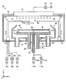
- FIG. 2 is a schematic side view showing a configuration example of the damage layer removing apparatus.
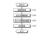
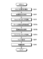
- FIG. 3 is a flowchart illustrating an example of a processing procedure for substrate processing executed in the substrate processing system.
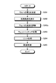
- FIG. 4 is a flowchart illustrating an example of a processing procedure of a damage layer removal process executed in the damage layer removal apparatus.
- FIG. 5A is an explanatory diagram of the operation of the damage layer removing apparatus.
- FIG. 5B is an operation explanatory diagram of the damage layer removing apparatus.
- FIG. 5C is an operation explanatory diagram of the damage layer removing apparatus.
- FIG. 5D is an explanatory diagram of the operation of the damaged layer removing apparatus.
- FIG. 5A is an explanatory diagram of the operation of the damage layer removing apparatus.
- FIG. 5B is an operation explanatory diagram of the damage layer removing apparatus.
- FIG. 5C is an
- FIG. 6A is an operation explanatory diagram of the damage layer removing apparatus.
- FIG. 6B is an operation explanatory diagram of the damage layer removing apparatus.
- FIG. 6C is an operation explanatory diagram of the damage layer removing apparatus.
- FIG. 7A is an operation explanatory diagram of the damage layer removing apparatus.
- FIG. 7B is an explanatory diagram of the operation of the damage layer removing apparatus.
- FIG. 7C is an operation explanatory diagram of the damage layer removing apparatus.
- FIG. 7D is an operation explanatory diagram of the damage layer removing apparatus.
- FIG. 8 is a diagram illustrating an example of the relationship between the thickness of the wafer and the supply amount of the processing liquid.
- FIG. 9 is a diagram illustrating an example of the relationship between the thickness of the wafer and the supply time of the processing liquid.
- FIG. 10 is a flowchart illustrating an example of a processing procedure of a damage layer removal process executed in the damage layer removal apparatus according to the third embodiment.
- FIG. 11 is a schematic side view showing a configuration example of a damage layer removing apparatus according to the fourth embodiment.
- FIG. 12 is a flowchart illustrating an example of a processing procedure of a damage layer removal process executed in the damage layer removal apparatus according to the fourth embodiment.
- FIG. 13 is an operation explanatory diagram of the damage layer removing apparatus according to the fourth embodiment.
- FIG. 14 is an explanatory diagram of the operation of the damaged layer removing apparatus according to the fourth embodiment.
- FIG. 1 is a diagram illustrating a schematic configuration of a substrate processing system according to the first embodiment.
- the X axis, the Y axis, and the Z axis that are orthogonal to each other are defined, and the positive direction of the Z axis is the vertically upward direction.
- a substrate processing system 1 according to this embodiment shown in FIG. 1 is a system for thinning a substrate.
- the substrate processing system 1 is an example of a substrate processing apparatus.
- the substrate processing system 1 includes a carry-in / out station 2 and a processing station 3.
- the loading / unloading station 2 and the processing station 3 are arranged in the order of the loading / unloading station 2 and the processing station 3 along the positive direction of the X axis.
- the loading / unloading station 2 includes a mounting table 10 and a transfer area 20.
- the mounting table 10 includes a plurality of mounting plates 11. On each mounting plate 11, a carrier C that stores a plurality of substrates, in this embodiment, a semiconductor substrate W such as a silicon wafer (hereinafter sometimes referred to as “wafer W”) in a horizontal state is mounted.
- wafer W a semiconductor substrate W such as a silicon wafer
- the conveyance area 20 is arranged adjacent to the X-axis positive direction side of the mounting table 10.
- a conveyance path 21 extending in the Y-axis direction and a conveyance device 22 movable along the conveyance path 21 are provided.
- the transfer device 22 is also movable in the X-axis direction and can be swung around the Z-axis. Between the carrier C mounted on the mounting plate 11 and a third processing block G3 of the processing station 3 described later. Then, the wafer W is transferred.
- the number of carriers C placed on the placement plate 11 is not limited to the illustrated one.
- a carrier or the like for collecting a substrate in which a problem has occurred may be placed on the placement plate 11.
- the processing station 3 is provided with a plurality of, for example, three processing blocks G1, G2, G3 provided with various devices.
- the first processing block G1 is provided on the back side of the processing station 3 (Y-axis positive direction side in FIG. 1), and the second side is provided on the front side of the processing station 3 (Y-axis negative direction side in FIG. 1).
- a processing block G2 is provided.
- a third processing block G3 is provided on the loading / unloading station 2 side of the processing station 3 (X-axis negative direction side in FIG. 1).
- a rough grinding device 31 and a finish grinding device 32 are arranged.
- the rough grinding device 31 and the finish grinding device 32 are examples of a grinding unit.
- the rough grinding device 31 performs a rough grinding process on the wafer W.
- the rough grinding apparatus 31 includes, for example, a chuck (not shown) that holds the wafer W therein, and the surface of the wafer W held by the chuck is brought into contact with a grinding wheel (not shown). In this state, the surface is roughly ground by rotating the chuck and the grinding wheel.
- a grinding liquid such as water is supplied to the surface of the wafer W.
- the finish grinding device 32 performs finish grinding on the wafer W.
- the specific configuration of the finish grinding device 32 is substantially the same as the configuration of the rough grinding device 31.
- the particle size of the grinding wheel (not shown) in the finish grinding device 32 is preferably set smaller than the particle size of the grinding wheel of the rough grinding device 31.
- the finish grinding apparatus 32 configured as described above performs grinding with the chuck while supplying the grinding liquid to the surface of the wafer W held by a chuck (not shown) while the surface is in contact with a grinding wheel having a small particle size.
- the surface is finish ground by rotating the grinding wheel.
- the configurations of the rough grinding device 31 and the finish grinding device 32 are not limited to the above, and may be a configuration in which the wafer W is ground by other methods such as CMP (Chemical Mechanical Polishing).
- the thickness of the wafer W after grinding is measured, and the processing conditions for the wet etching process are determined based on the measured thickness of the wafer W. did. Thereby, the flatness of the surface can be improved in the wafer W after the damaged layer is removed.
- a damage layer removing device 33 and a cleaning device 34 are arranged in the second processing block G2 of the substrate processing system 1.
- the damaged wafer removing apparatus 33 carries the ground wafer W, supplies a processing liquid to the wafer W, performs wet etching, and removes the damaged layer formed on the surface of the wafer W.
- the configuration of the damage layer removing device 33 will be described later with reference to FIG.
- the arrangement position of the damage layer removal apparatus 33 shown in FIG. 1 is an illustration and is not limited. That is, for example, the damage layer removing device 33 may be arranged in the first processing block G1 or the third processing block G3. Further, for example, a new station is provided between the position of the processing station 3 on the positive side of the X-axis or between the loading / unloading station 2 and the processing station 3, and the damage layer removing device 33 is disposed at the new station. May be.
- the damaged layer removing device 33 is an example of a damaged layer removing unit.
- the cleaning device 34 includes, for example, a chuck (not shown) that holds the wafer W therein, and supplies cleaning liquid such as DIW (pure water) to the front and back surfaces of the wafer W while rotating the chuck and the wafer W. Thereby, the surface of the wafer W and the like are cleaned.
- the cleaning device 34 is not limited to the configuration described above.
- a wafer W transition device 35 is provided in the third processing block G3.
- a transfer area 40 is formed in an area surrounded by the first processing block G1 to the third processing block G3 configured as described above.
- a transport device 41 is disposed in the transport region 40.
- the transfer device 41 has a transfer arm that can move around the vertical direction, the horizontal direction, and the vertical axis, for example.
- the transfer apparatus 41 moves in the transfer area 40 and transfers the wafer W to a predetermined apparatus in the first process block G1, the second process block G2, and the third process block G3 adjacent to the transfer area 40.
- the substrate processing system 1 includes a control device 100.
- the control device 100 is a computer, for example, and includes a control unit 101 and a storage unit 102.
- the storage unit 102 stores a program for controlling various processes executed in the substrate processing system 1.
- the control unit 101 controls the operation of the substrate processing system 1 by reading and executing a program stored in the storage unit 102.
- Such a program may be recorded on a computer-readable storage medium and may be installed in the storage unit 102 of the control device 100 from the storage medium.
- Examples of the computer-readable storage medium include a hard disk (HD), a flexible disk (FD), a compact disk (CD), a magnetic optical disk (MO), and a memory card.
- FIG. 2 is a schematic side view showing a configuration example of the damage layer removing device 33.
- the damaged layer removing apparatus 33 includes a chamber 50, a substrate holding mechanism 60, a processing liquid supply unit 70, a measuring mechanism 80, and a recovery cup 90.
- the chamber 50 accommodates the substrate holding mechanism 60, the processing liquid supply unit 70, the measurement mechanism 80, and the recovery cup 90.
- An FFU (Fan Filter Unit) 51 is provided on the ceiling of the chamber 50.
- An inert gas supply source 53 is connected to the FFU 51 via a valve 52. Then, the FFU 51 discharges an inert gas such as N 2 gas supplied from the inert gas supply source 53 into the chamber 50 to form a down flow.
- the substrate holding mechanism 60 includes a holding part 61, a support part 62, and a driving part 63.
- the holding unit 61 holds the wafer W horizontally. Specifically, a holding member 611 that holds the wafer W from the side surface is provided on the upper surface of the holding unit 61. The wafer W is horizontally held by the holding member 611 while being slightly separated from the upper surface of the holding unit 61. The wafer W is held by the holding unit 61 with the surface on which the damaged layer is formed by grinding facing upward.
- the column part 62 is a member extending in the vertical direction, and a base end part is rotatably supported by the drive part 63, and the holding part 61 is horizontally supported at the tip part.
- the drive unit 63 rotates the column unit 62 around the vertical axis.
- an electric motor is used as the drive unit 63.
- the substrate holding mechanism 60 configured as described above rotates the support part 62 by rotating the support part 62 using the drive part 63, thereby rotating the support part 61 supported by the support part 62.
- the wafer W is rotated.
- the treatment liquid supply unit 70 includes nozzles 71 a and 71 b, an arm 72 that horizontally supports the nozzles 71 a and 71 b, and a swivel lifting mechanism 73 that swivels and lifts the arm 72.
- the processing liquid supply unit 70 supplies a processing liquid (here, hydrofluoric acid) used for the wet etching process to the wafer W from the nozzle 71a, and supplies DIW, which is a type of rinsing liquid, from the nozzle 71b.
- a processing liquid here, hydrofluoric acid
- DIW which is a type of rinsing liquid
- the above-described treatment liquid includes a plurality of types of chemical liquids (here, hydrofluoric acid (HF) and nitric acid (HNO3)).
- a hydrofluoric acid supply source 75a is connected to the nozzle 71a via a valve 74a
- a nitric acid supply source 75b is connected via a valve 74b
- a DIW supply source 75c is connected to the nozzle 71b via a valve 74c.
- the hydrofluoric acid supplied from the nozzle 71a has a predetermined mixing ratio by controlling the opening degree of the valves 74a and 74b by the control device 100.
- the state of the wafer W after the wet etching process changes depending on the mixing ratio.
- the surface of the wafer W is etched with sharp corners.
- the corners of the surface of the wafer W are rounded and etched into a flat state.
- the opening degree of the valves 74a and 74b is controlled so that hydrofluoric acid having a higher ratio of nitric acid than hydrofluoric acid is supplied from the nozzle 71a, thereby improving the flatness of the surface of the wafer W.
- the mixing ratio of hydrofluoric acid and nitric acid is set to 0.3 to 3: 9.7 to 7, and preferably set to 1: 9.
- the damaged layer of the wafer W can be efficiently removed by isotropic etching.
- the opening degree of the valves 74a and 74b is controlled to adjust the nitric acid to a predetermined mixing ratio.
- the present invention is not limited to this.
- the nozzle 71a is previously mixed at a predetermined mixing ratio.
- a supply source of hydrofluoric acid may be connected.
- the nozzles 71a and 71b do not need to be separate nozzles, and may be the same nozzle, for example.
- the measurement mechanism 80 includes a measurement unit 81 that measures the thickness of the wafer W, an arm 82 that horizontally supports the measurement unit 81, and a turning lift mechanism 83 that turns and lifts the arm 82. And the measurement part 81 is moved above the wafer W using the turning raising / lowering mechanism 83, Thereby, the thickness of the whole wafer W can be measured.
- a spectral interference type thickness measuring device can be used, but is not limited thereto, and may be another thickness measuring device such as a laser displacement meter or a capacitance sensor.
- the collection cup 90 is disposed so as to surround the holding unit 61, and collects the processing liquid scattered from the wafer W by the rotation of the holding unit 61.
- a drainage port 91 is formed at the bottom of the recovery cup 90, and the processing liquid collected by the recovery cup 90 is discharged from the drainage port 91 to the outside of the damage layer removing device 33.
- an exhaust port 92 for discharging the gas supplied from the FFU 51 to the outside of the damage layer removing device 33 is formed at the bottom of the recovery cup 90.
- FIG. 3 is a flowchart showing an example of the processing procedure of the substrate processing executed in the substrate processing system 1. 3 is executed by the control unit 101 of the control device 100, for example.
- the control unit 101 takes out the wafer W before being thinned in the carrier C by the transfer device 22 (see FIG. 1) of the loading / unloading station 2 and performs the third processing in the processing station 3. It is transferred to the transition device 35 (see FIG. 1) of the block G3.
- the controller 101 transports the wafer W of the transition device 35 to the rough grinding device 31 of the first processing block G1 by the transport device 41 (see FIG. 1).
- control unit 101 performs a rough grinding process on the wafer W in the rough grinding apparatus 31 (step S101).
- control unit 101 transports the roughly ground wafer W to the finish grinding device 32 by the transport device 41, and performs finish grinding processing on the wafer W (step S102).
- control unit 101 transports the wafer W, which has been finish-ground by the finish grinding device 32, to the damaged layer removing device 33 by the transport device 41.
- the wafer W transferred to the damaged layer removing apparatus 33 is held by the holding unit 61 (see FIG. 2).
- the wafer W is held by the holding unit 61 with the ground surface facing upward.
- the control part 101 performs the process which supplies a process liquid with respect to the wafer W, performs a wet etching process within the damage layer removal apparatus 33, and removes the damage layer of the wafer W (step S103).
- control unit 101 performs processing for transporting the wafer W from which the damaged layer has been removed by the damaged layer removing device 33 to the cleaning device 34 by the transport device 41 and cleaning the surface of the wafer W (step S104).
- control unit 101 unloads the cleaned wafer W from the cleaning device 34 by the transfer device 41 and transfers it to the transition device 35. And the control part 101 returns the processed wafer W in the transition apparatus 35 to the carrier C of the mounting board 11 by the conveying apparatus 22, and a series of substrate processes are complete
- FIG. 4 is a flowchart illustrating an example of a processing procedure of the damage layer removal process executed in the damage layer removal apparatus 33.
- 5A to 5D are explanatory diagrams of the operation of the damaged layer removing apparatus 33.
- FIG. 4 is a flowchart illustrating an example of a processing procedure of the damage layer removal process executed in the damage layer removal apparatus 33.
- 5A to 5D are explanatory diagrams of the operation of the damaged layer removing apparatus 33.
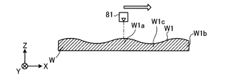
- the control unit 101 measures the thickness of the ground wafer W by the measuring unit 81 (step S201). Specifically, the control unit 101 moves the measurement unit 81 and measures the thickness of the entire wafer W as shown in FIG. 5A. Note that the thickness of the wafer W may be measured without rotating the wafer W or while rotating the wafer W.
- the shape of the wafer W after grinding is a shape in which the central portion W1a of the surface W1 is recessed in the negative direction of the Z axis from the peripheral portion W1b as shown in FIG. 5A
- the thickness Tb of the peripheral portion W1b of the wafer W is thicker than the thickness Ta of the central portion W1a
- Tb> Ta the thickness variation of the wafer W caused by grinding is exaggerated for convenience of understanding.
- control unit 101 determines the processing conditions for the wet etching process based on the measured thickness of the wafer W (Step S202), and supplies the processing liquid to the ground wafer W based on the determined processing conditions. Supply the wet etching process (step S203). The damaged layer formed on the wafer W is removed by the wet etching process.
- the control unit 101 is an example of a condition determining unit.
- the processing conditions of the above-described wet etching process include, for example, at least one of the operation of the nozzle 71a that supplies the processing liquid, the rotation speed of the wafer W, the supply amount of the processing liquid, and the supply time of the processing liquid. It is preferably included.
- the contents of the processing conditions described above are merely examples and are not limited, and are other contents as long as they affect the wet etching process, for example, the etching rate. Also good.
- the control unit 101 determines the operation of the nozzle 71a and the rotation speed of the wafer W according to the thickness of the wafer W. Was changed.
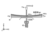
- control unit 101 positions the nozzle 71a above the center of the wafer W. Thereafter, the control unit 101 opens the valves 74a and 74b (see FIG. 2) to supply hydrofluoric acid as a processing liquid from the nozzle 71a to the surface W1 of the wafer W (see FIG. 5B).
- control unit 101 rotates the holding unit 61 by the driving unit 63 and rotates the wafer W held by the holding unit 61.
- the processing liquid supplied to the wafer W spreads on the surface W1 of the wafer W due to the centrifugal force accompanying the rotation of the wafer W, and the surface W1 is entirely etched.
- the rotation speed of the wafer W is the first rotation speed set to a relatively low value.
- the control unit 101 moves the nozzle 71a from the central portion W1a to the peripheral portion W1b of the wafer W while the processing liquid is supplied from the nozzle 71a (see FIGS. 5C and 5D). Due to the movement of the nozzle 71a, in the vicinity of the central portion W1a of the surface W1 of the wafer W, the processing liquid is not supplied and is not etched or is not easily etched. On the other hand, in the vicinity of the peripheral edge W1b in the surface W1 of the wafer W, the processing liquid is supplied, and thus etching is continued.
- the vicinity of the thick peripheral edge W1b is etched more than the vicinity of the thin central part W1a, so that the wafer W can be brought close to a uniform thickness as a whole.
- the flatness of the surface W1 can be improved.
- the flatness can be expressed by, for example, TTV (total thickness variation: difference between the maximum value and the minimum value of the thickness of the entire surface of the wafer W).
- TTV total thickness variation: difference between the maximum value and the minimum value of the thickness of the entire surface of the wafer W.
- TTV can be reduced, that is, flatness can be improved by performing wet etching under the above-described processing conditions.
- the nozzle 71a is moved from the central portion W1a toward the peripheral portion W1b, The wafer W was rotated at a relatively low first rotational speed.
- shape of the wafer W after grinding is not limited to the example shown in FIG. 5A.
- 6A to 6C are operation explanatory views of the damaged layer removing apparatus 33 when the shape of the wafer W after grinding is different from the example shown in FIG. 5A.
- the case where the shape of the wafer W after grinding is a shape in which the central portion W1a of the surface W1 protrudes in the positive direction of the Z-axis from the peripheral edge portion W1b is taken as an example.
- a case where the thickness Tb of the peripheral portion W1b of the wafer W is thinner than the thickness Ta of the central portion W1a is taken as an example (Tb ⁇ Ta).
- control unit 101 first measures the thickness of the ground wafer W by the measuring unit 81 (see FIG. 6A). Then, the control unit 101 determines the operation of the nozzle 71a and the rotation speed of the wafer W as processing conditions for the wet etching process based on the measured thickness of the wafer W, and performs the wet etching process under the processing conditions.
- control unit 101 positions the nozzle 71a above the center of the wafer W. Thereafter, the controller 101 opens the valves 74a and 74b, and supplies the processing liquid from the nozzle 71a to the surface W1 of the wafer W (see FIG. 6B).
- control unit 101 rotates the holding unit 61 (see FIG. 2) at the second rotation number set to a value higher than the first rotation number described above, and rotates the wafer W held by the holding unit 61. .
- the processing liquid supplied to the wafer W spreads on the surface W1 of the wafer W due to the centrifugal force accompanying the rotation of the wafer W, and the surface W1 is entirely etched.
- control unit 101 continues to supply the processing liquid without moving the nozzle 71a (see FIG. 6C).
- the wafer W is continuously etched in the vicinity of the thick central portion W1a.
- the processing liquid spreading near the peripheral edge W1b is spun off in a shorter time than when rotating at the first rotation speed.
- the vicinity of the thick central portion W1a is etched more than the vicinity of the thin peripheral portion W1b, so that the wafer W can be brought close to a uniform thickness as a whole.
- the flatness of the surface W1 can be improved.
- FIGS. 7A to 7D are operation explanatory views of the damage layer removing apparatus 33 when the shape of the wafer W after grinding is different from the example shown in FIGS. 5A and 6A.
- control unit 101 first measures the thickness of the ground wafer W by the measurement unit 81 (see FIG. 7A). Then, the control unit 101 determines the operation of the nozzle 71a and the rotation speed of the wafer W as processing conditions for the wet etching process based on the measured thickness of the wafer W, and performs the wet etching process under the processing conditions.
- control unit 101 positions the nozzle 71a above the center of the wafer W. Thereafter, the controller 101 opens the valves 74a and 74b, and supplies the processing liquid from the nozzle 71a to the surface W1 of the wafer W (see FIG. 7B).
- the control unit 101 rotates the holding unit 61 (see FIG. 2) at the first rotation number, and rotates the wafer W held by the holding unit 61. Thereby, the processing liquid supplied to the wafer W spreads on the surface W1 of the wafer W, and the surface W1 is etched as a whole.
- the rotation speed of the wafer W is the first rotation speed.
- the rotation speed is not limited to this, and may be a rotation speed set to a value other than the second rotation speed or the first and second rotation speeds. .
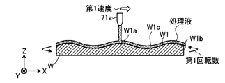
- control unit 101 moves the nozzle 71a from the central portion W1a of the wafer W toward the peripheral portion W1b at a first speed set to a relatively low value while the processing liquid is being supplied from the nozzle 71a.
- the wafer W is sufficiently etched in the vicinity of the thick central portion W1a.
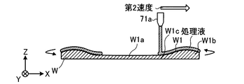
- the control unit 101 moves the nozzle 71a at the second speed set to a value higher than the first speed. Due to the movement of the nozzle 71a, in the vicinity of the intermediate portion W1c of the surface W1 of the wafer W, the supply amount of the processing liquid is smaller than the other portions, and the etching amount is also reduced.
- the control unit 101 moves the nozzle 71a back to the relatively low first speed. Thereby, in the wafer W, sufficient etching is performed in the vicinity of the thick peripheral edge W1b.
- the nozzle 71a that has reached the vicinity of the peripheral edge W1b is moved at the first speed.
- the present invention is not limited to this. For example, other speeds may be used as long as the speed is lower than the second speed. .
- the thick central portion W1a and the peripheral portion W1b are etched more than the thin intermediate portion W1c, and the wafer W can be made close to a uniform thickness as a whole.
- the flatness of the surface W1 of the wafer W can be improved.
- the processing conditions are determined according to the thickness of the wafer W. Specifically, the operation of the nozzle 71a such as the presence / absence and movement of the nozzle 71a, and the rotation of the wafer W The number was changed. Thereby, the flatness of the surface W1 of the wafer W can be improved.
- FIG. 8 is a diagram illustrating an example of the relationship between the thickness of the wafer W and the supply amount of the processing liquid.
- the supply amount of the processing liquid is set to increase as the thickness of the wafer W increases. Therefore, when the control unit 101 determines the supply amount of the processing liquid in the example shown in FIG. 8 based on the thickness of the wafer W, a large amount of processing liquid is supplied to the thick portion of the wafer W, while the thin portion A smaller amount of processing liquid is supplied than in the thick part.
- the wafer W a thick part is etched more than a thin part, and the wafer W can be brought close to a shape having a uniform thickness as a whole. Therefore, the flatness of the surface W1 of the wafer W is increased. Can be improved.
- FIG. 9 is a diagram illustrating an example of the relationship between the thickness of the wafer W and the supply time of the processing liquid.
- the processing liquid supply time is set to become longer as the thickness of the wafer W increases. Therefore, when the control unit 101 determines the supply time of the processing liquid in the example illustrated in FIG. 9 based on the thickness of the wafer W, the processing liquid is supplied to the thick portion of the wafer W for a long time while the processing liquid is thin. The processing solution is supplied to the part for a shorter time than the thick part.
- the wafer W a thick part is etched more than a thin part, and the wafer W can be brought close to a shape having a uniform thickness as a whole. Therefore, the flatness of the surface W1 of the wafer W is increased. Can be improved.
- the graphs shown in FIGS. 8 and 9 are merely examples and are not limited.
- the processing conditions of the wet etching process are optimized, and the surface W1 of the wafer W is optimized.
- the flatness was improved.
- control unit 101 subsequently performs a rinsing process on the wafer W from which the damaged layer has been removed (step S ⁇ b> 204).
- the control unit 101 opens the valve 74c for a predetermined time and rotates the wafer W at a predetermined rotation speed.
- DIW supplied from the DIW supply source 75c is supplied from the nozzle 71b to the surface W1 of the wafer W, so that the processing liquid remaining on the wafer W is washed away by the DIW and the wet etching process is stopped.
- control unit 101 performs a drying process (step S205).
- a drying process the control unit 101 dries the DIW on the wafer W by increasing the number of rotations of the wafer W to dry the wafer W.
- the substrate processing method includes a grinding process, a measurement process, a condition determination process, and a damage layer removal process.
- the grinding process the surface W1 of the wafer W is ground.
- the measuring step the thickness of the ground wafer W is measured.
- the condition determining step the processing conditions for the wet etching process performed on the wafer W are determined based on the measured thickness of the wafer W.
- a processing liquid is supplied to the ground wafer W based on the determined processing conditions to perform wet etching, and the damaged layer formed on the surface W1 of the wafer W is removed.
- the processing conditions of the wet etching process can be optimized based on the thickness of the ground wafer W, and thus the flatness of the surface W1 can be improved in the wafer W after removing the damaged layer. Furthermore, by optimizing the processing conditions of the wet etching process, the surface roughness of the wafer W after removal of the damaged layer can also be improved (specifically reduced).
- the surface W1 of the wafer W can be set to the intended flatness regardless of the grinding accuracy in the finish grinding apparatus 32, and the yield can be increased. It can also be improved.
- the damaged layer removing apparatus 33 of the substrate processing system 1 in the second embodiment is configured to be able to supply a plurality of types of processing liquids to the wafer W, and supply the wafer W based on the measured thickness of the wafer W.
- the type of liquid was changed.
- an acetic acid (CH3COOH) supply source 75d is connected to the nozzle 71a via a valve 74d.
- the control unit 101 can also dilute by adding acetic acid to hydrofluoric acid (treatment liquid) in which hydrofluoric acid and nitric acid are mixed by opening the valve 74d.
- hydrofluoric acid treatment liquid
- the hydrofluoric acid in which hydrofluoric acid and nitric acid are mixed may be referred to as a “first treatment liquid”
- the treatment liquid obtained by adding acetic acid to the hydrofluoric acid may be referred to as a “second treatment liquid”.
- the mixing ratio of hydrofluoric acid, nitric acid and acetic acid in the second treatment liquid can be arbitrarily set, but is set to, for example, 1 to 1.5: 3 to 4.5: 1 to 2.5. .
- the etching rate of the second processing liquid mixed as described above is higher than that of the first processing liquid. Therefore, the control unit 101 according to the second embodiment determines the processing liquid to be supplied to the wafer W from the first and second processing liquids based on the thickness of the ground wafer W.
- the control unit 101 supplies the first processing liquid to the vicinity of the thin central portion W1a, and supplies the second processing liquid to the vicinity of the thick peripheral portion W1b.
- the operation of the valves 74a, 74b, 74d is controlled.
- the vicinity of the thick peripheral edge W1b is etched more than the vicinity of the thin central part W1a, so that the wafer W can be brought close to a uniform thickness as a whole.
- the flatness of the surface W1 can be further improved.
- the control unit 101 uses a plurality of types of processing liquids as processing conditions based on the thickness of the wafer W.
- the processing liquid supplied to the wafer W was determined from the inside.
- the two types of treatment liquids are the first and second treatment liquids, but the present invention is not limited to this, and three or more kinds may be used.
- the substrate processing system 1 according to the third embodiment will be described.
- the thickness of the wafer W is measured again during the wet etching process of the wafer W, and the processing conditions of the wet etching process are changed based on the re-measured thickness of the wafer W. I tried to do it.
- FIG. 10 is a flowchart illustrating an example of a processing procedure of a damage layer removal process executed in the damage layer removal apparatus 33 according to the third embodiment.
- control unit 101 performs the above-described processing of steps S201 to S203.
- control unit 101 measures the thickness of the wafer W again by the measuring unit 81 while the wet etching process is being performed in step S203 (step S203a).
- control unit 101 changes the processing condition determined in step S202 based on the thickness of the wafer W obtained by remeasurement (step S203b). Specifically, for example, an increase / decrease in the moving speed of the nozzle 71a, an increase / decrease in the number of rotations of the wafer W, an increase / decrease in the supply amount of the processing liquid, an increase / decrease in the supply time of the processing liquid are performed. And the control part 101 performs a wet etching process based on the changed process conditions (step S203c).
- the processing conditions of the wet etching process can be modified according to the etching reaction state on the surface W1 of the wafer W, and further optimization can be achieved. Since the remaining effects are the same as those in the previous embodiment, description thereof is omitted.
- the thickness of the wafer W is measured again during the wet etching process.
- the present invention is not limited to this.
- the thickness may be measured again after the wet etching process.
- a substrate processing system 1 according to the fourth embodiment Next, a substrate processing system 1 according to the fourth embodiment will be described.
- a mechanism capable of adjusting the temperature of the wafer W is provided, and the temperature of the wafer W is adjusted based on the measured thickness of the wafer W. I tried to do it.
- FIG. 11 is a schematic side view showing a configuration example of the damage layer removing apparatus 33 according to the fourth embodiment.
- the substrate holding mechanism 60 of the damaged layer removing apparatus 33 includes a fluid supply unit 64 that supplies a fluid to the wafer W and adjusts the temperature of the wafer W.
- the fluid supply part 64 is a long member inserted through a hollow part 621 formed in the center of the column part 62, and a flow path 641 is formed inside.
- a CDIW supply source 115a is connected to the flow path 641 through a valve 114a, and an HDIW supply source 115b is connected through a valve 114b.
- the fluid supply unit 64 supplies CDIW or HDIW supplied from the supply sources 115 a and 115 b to the back surface of the wafer W through the flow path 641.
- CDIW is, for example, room temperature pure water.
- HDIW is pure water heated to a temperature higher than that of CDIW.
- the fluid supplied from the fluid supply unit 64 to the back surface of the wafer W is pure water.
- the present invention is not limited to this, and other types of fluid such as N 2 gas may be used.
- FIG. 12 is a flowchart showing an example of the processing procedure of the damage layer removal process executed in the damage layer removal apparatus 33 configured as described above.
- control unit 101 performs the processes of steps S ⁇ b> 201 and S ⁇ b> 202 described above.
- the control unit 101 supplies a fluid to the wafer W based on the thickness of the wafer W measured in step S201 to adjust the temperature of the wafer W (step S202a), and then performs a wet etching process. (Step S203).
- steps S202a and S203 will be specifically described with reference to FIG. 13 and FIG. 13 and 14 are explanatory diagrams of the operation of the damaged layer removing apparatus 33 according to the fourth embodiment.
- the control unit 101 opens the valve 114a (see FIG. 11) to open the wafer from the fluid supply unit 64.
- CDIW is supplied to the vicinity of the central portion W1a on the back surface of W.
- CDIW is supplied to the vicinity of the central portion W1a on the back surface of the wafer W, so that a temperature rise due to reaction heat in the vicinity of the central portion W1a can be suppressed. It is possible to suppress the etching from being accelerated in the vicinity of W1a.
- the vicinity of the thick peripheral edge W1b is etched more than the vicinity of the thin central part W1a, so that the wafer W can be brought close to a uniform thickness as a whole.
- the flatness of the surface W1 can be further improved.
- the control unit 101 opens the valve 114b (see FIG. 11) to open the fluid supply unit 64.
- HDIW is supplied to the vicinity of the central portion W1a on the back surface of the wafer W.
- the temperature of the central portion W1a can be raised, and thus the etching in the vicinity of the central portion W1a can be further promoted.
- the vicinity of the thick central portion W1a is etched more than the vicinity of the thin peripheral portion W1b, so that the wafer W can be brought close to a uniform thickness as a whole.
- the flatness of the surface W1 can be further improved.
- the fluid is supplied from the fluid supply unit 64 to the vicinity of the central portion W1a on the back surface of the wafer W.
- the present invention is not limited to this. That is, for example, a plurality of fluid supply parts 64 are provided at positions corresponding to the central part W1a, the peripheral edge part W1b, and the intermediate part W1c of the wafer W, and the fluid supply parts 64 to which the fluid is to be supplied from the plurality of fluid supply parts 64 are provided. An appropriate selection may be made based on the thickness of the wafer W.
- the fluid supply unit 64 is configured to supply two types of fluids, CDIW and HDIW, to the wafer W.
- the present invention is not limited to this, and any one type or three or more types of fluids are supplied to the wafer W. You may make it supply.
- the numbers and arrangement positions of the rough grinding device 31, the finish grinding device 32, the damaged layer removing device 33, and the cleaning device 34 are shown in FIG. It is not restricted to an example, You may set arbitrarily.
- the rough grinding device 31, the finish grinding device 32, the damaged layer removing device 33, and the cleaning device 34 are separate devices, but the present invention is not limited to this. For example, one or two It may be combined into two or more devices.
- the measurement unit 81 is provided in the damaged layer removing device 33.
- the measurement unit 81 is not limited thereto.
- the measurement unit 81 is provided in the finish grinding device 32, and the thickness of the wafer W is increased during the finish grinding process. You may make it measure.
- the wafer W described above may be a superposed substrate in which, for example, a wafer on which an electronic circuit is formed and a bare wafer on which an electronic circuit is not formed are bonded.
- the first to fourth embodiments described above may be combined. That is, for example, by combining the second embodiment and the fourth embodiment, the control unit 101 determines the type of processing liquid to be supplied to the wafer W based on the thickness of the wafer W, and the wafer W The temperature may be adjusted.
- processing liquid supplied to the wafer W in the first, third, and fourth embodiments may be the second processing liquid in the second embodiment.
Landscapes
- Engineering & Computer Science (AREA)
- Mechanical Engineering (AREA)
- Weting (AREA)
- Constituent Portions Of Griding Lathes, Driving, Sensing And Control (AREA)
- Grinding Of Cylindrical And Plane Surfaces (AREA)
- Mechanical Treatment Of Semiconductor (AREA)
- Cleaning Or Drying Semiconductors (AREA)
Abstract
実施形態の一態様に係る基板処理方法は、研削工程と、測定工程と、条件決定工程と、ダメージ層除去工程とを含む。研削工程は、基板(W)の表面(W1)を研削する。測定工程は、研削された基板の厚さを測定する。条件決定工程は、測定された基板の厚さに基づき、基板に対して行われるウェットエッチング処理の処理条件を決定する。ダメージ層除去工程は、決定された処理条件に基づいて、研削された基板に処理液を供給してウェットエッチング処理を行い、基板の表面に形成されたダメージ層を除去する。
Description
開示の実施形態は、基板処理方法および基板処理装置に関する。
近年、たとえば、半導体デバイスの製造工程において、シリコンウェハなどの半導体基板の表面を研削し、基板の薄型化を図る技術が提案されている(たとえば、特許文献1参照)。また、上記した従来技術にあっては、研削によって基板の表面に形成されたダメージ層を、ウェットエッチング処理などにより除去するようにしている。
しかしながら、上述した従来技術には、ダメージ層が除去された後の基板において、表面の平坦度を向上させるという点で更なる改善の余地があった。
実施形態の一態様は、ダメージ層除去後の基板において、表面の平坦度を向上させることができる基板処理方法および基板処理装置を提供することを目的とする。
実施形態の一態様に係る基板処理方法は、研削工程と、測定工程と、条件決定工程と、ダメージ層除去工程とを含む。研削工程は、基板の表面を研削する。測定工程は、研削された前記基板の厚さを測定する。条件決定工程は、測定された前記基板の厚さに基づき、前記基板に対して行われるウェットエッチング処理の処理条件を決定する。ダメージ層除去工程は、決定された前記処理条件に基づいて、研削された前記基板に処理液を供給してウェットエッチング処理を行い、前記基板の表面に形成されたダメージ層を除去する。
実施形態の一態様によれば、ダメージ層除去後の基板において、表面の平坦度を向上させることができる。
以下、添付図面を参照して、本願の開示する基板処理方法および基板処理装置の実施形態を詳細に説明する。なお、以下に示す実施形態によりこの発明が限定されるものではない。
(第1の実施形態)
<1.基板処理システムの構成>
図1は、第1の実施形態に係る基板処理システムの概略構成を示す図である。以下では、位置関係を明確にするために、互いに直交するX軸、Y軸およびZ軸を規定し、Z軸正方向を鉛直上向き方向とする。
<1.基板処理システムの構成>
図1は、第1の実施形態に係る基板処理システムの概略構成を示す図である。以下では、位置関係を明確にするために、互いに直交するX軸、Y軸およびZ軸を規定し、Z軸正方向を鉛直上向き方向とする。
図1に示す本実施形態に係る基板処理システム1は、基板を薄型化するシステムである。なお、基板処理システム1は、基板処理装置の一例である。
図1に示すように、基板処理システム1は、搬入出ステーション2と、処理ステーション3とを備える。搬入出ステーション2および処理ステーション3は、X軸正方向に沿って、搬入出ステーション2および処理ステーション3の順番で並べて配置される。
搬入出ステーション2は、載置台10と、搬送領域20とを備える。載置台10は、複数の載置板11を備える。各載置板11には、複数枚の基板、本実施形態ではたとえばシリコンウェハなどの半導体基板W(以下「ウェハW」という場合がある)を水平状態で収容するキャリアCが載置される。
搬送領域20は、載置台10のX軸正方向側に隣接して配置される。かかる搬送領域20には、Y軸方向に延在する搬送路21と、搬送路21に沿って移動可能な搬送装置22とが設けられる。搬送装置22は、X軸方向にも移動可能かつZ軸周りに旋回可能であり、載置板11に載置されたキャリアCと、後述する処理ステーション3の第3処理ブロックG3との間で、ウェハWの搬送を行う。
なお、載置板11に載置されるキャリアCの個数は、図示のものに限定されない。また、載置板11には、キャリアC以外に、不具合が生じた基板を回収するためのキャリア等が載置されてもよい。
処理ステーション3には、各種装置を備えた複数たとえば3つの処理ブロックG1,G2,G3が設けられる。たとえば処理ステーション3の背面側(図1のY軸正方向側)には、第1処理ブロックG1が設けられ、処理ステーション3の正面側(図1のY軸負方向側)には、第2処理ブロックG2が設けられる。また、処理ステーション3の搬入出ステーション2側(図1のX軸負方向側)には、第3処理ブロックG3が設けられる。
第1処理ブロックG1には、粗研削装置31と、仕上げ研削装置32とが配置される。なお、粗研削装置31と仕上げ研削装置32とは、研削部の一例である。
粗研削装置31は、ウェハWに対して粗研削処理を行う。具体的には、粗研削装置31は、たとえばウェハWを保持するチャック(図示せず)を内部に備え、チャックに保持されたウェハWの表面を研削砥石(図示せず)に当接させた状態で、チャックと研削砥石とをそれぞれ回転させることによって表面を粗研削する。なお、粗研削が行われる際、ウェハWの表面には、たとえば水などの研削液が供給される。
仕上げ研削装置32は、ウェハWに対して仕上げ研削処理を行う。具体的な仕上げ研削装置32の構成は、粗研削装置31の構成とほぼ同様である。但し、仕上げ研削装置32における研削砥石(図示せず)の粒度は、粗研削装置31の研削砥石の粒度より小さく設定されることが好ましい。
上記のように構成された仕上げ研削装置32は、図示しないチャックに保持されたウェハWの表面に研削液を供給しながら、表面を粒度の小さい研削砥石に当接させた状態で、チャックと研削砥石とをそれぞれ回転させることによって表面を仕上げ研削する。なお、粗研削装置31および仕上げ研削装置32の構成は、上記に限定されるものではなく、たとえばCMP(Chemical Mechanical Polishing)などその他の方法でウェハWを研削する構成であってもよい。
ところで、上記のようにウェハWの表面が研削砥石によって研削されると、ウェハWの表面には、たとえば微小な亀裂等の機械的なダメージのあるダメージ層が形成される。そのため、研削後のウェハWに対してダメージ層を除去するウェットエッチング処理が施される。そして、かかるダメージ層が除去された後のウェハWの表面にあっては、たとえば鏡面仕上げなど比較的高い平坦度が要求されるが、従来技術においては、表面の平坦度を向上させるという点で更なる改善の余地があった。
そこで、本実施形態に係る基板処理システム1にあっては、研削後のウェハWの厚さを測定し、測定されたウェハWの厚さに基づいてウェットエッチング処理の処理条件を決定するようにした。これにより、ダメージ層が除去された後のウェハWにおいて、表面の平坦度を向上させることができる。
以下詳しく説明すると、基板処理システム1の第2処理ブロックG2には、ダメージ層除去装置33と、洗浄装置34とが配置される。ダメージ層除去装置33には、研削されたウェハWが搬入され、かかるウェハWに対して処理液を供給してウェットエッチング処理を行い、ウェハWの表面に形成されたダメージ層を除去する。なお、ダメージ層除去装置33の構成については、図2以降を参照して後述する。
なお、図1で示したダメージ層除去装置33の配置位置は、例示であって限定されるものではない。すなわち、たとえば第1処理ブロックG1や第3処理ブロックG3にダメージ層除去装置33を配置してもよい。さらには、たとえば処理ステーション3のX軸正方向側の位置や、搬入出ステーション2と処理ステーション3との間に新たなステーションを設け、その新たなステーションにダメージ層除去装置33を配置するようにしてもよい。なお、ダメージ層除去装置33は、ダメージ層除去部の一例である。
洗浄装置34は、たとえばウェハWを保持するチャック(図示せず)を内部に備え、チャックおよびウェハWを回転させながら、DIW(純水)などの洗浄液をウェハWの表面や裏面へ供給する。これにより、ウェハWの表面等が洗浄される。なお、この洗浄装置34は、上記した構成に限定されるものではない。
第3処理ブロックG3には、ウェハWのトランジション装置35が設けられる。上記のように構成された第1処理ブロックG1~第3処理ブロックG3に囲まれた領域には、搬送領域40が形成される。搬送領域40には、搬送装置41が配置される。
搬送装置41は、たとえば鉛直方向、水平方向および鉛直軸周りに移動自在な搬送アームを有する。かかる搬送装置41は、搬送領域40内を移動し、搬送領域40に隣接する第1処理ブロックG1、第2処理ブロックG2および第3処理ブロックG3内の所定の装置にウェハWを搬送する。
また、基板処理システム1は、制御装置100を備える。制御装置100は、たとえばコンピュータであり、制御部101と記憶部102とを備える。記憶部102には、基板処理システム1において実行される各種の処理を制御するプログラムが格納される。制御部101は、記憶部102に記憶されたプログラムを読み出して実行することによって基板処理システム1の動作を制御する。
なお、かかるプログラムは、コンピュータによって読み取り可能な記憶媒体に記録されていたものであって、その記憶媒体から制御装置100の記憶部102にインストールされたものであってもよい。コンピュータによって読み取り可能な記憶媒体としては、たとえばハードディスク(HD)、フレキシブルディスク(FD)、コンパクトディスク(CD)、マグネットオプティカルディスク(MO)、メモリカードなどがある。
<2.ダメージ層除去装置の構成>
次に、ダメージ層除去装置33の構成について図2を参照して説明する。図2は、ダメージ層除去装置33の構成例を示す模式側面図である。
次に、ダメージ層除去装置33の構成について図2を参照して説明する。図2は、ダメージ層除去装置33の構成例を示す模式側面図である。
図2に示すように、ダメージ層除去装置33は、チャンバ50と、基板保持機構60と、処理液供給部70と、測定機構80と、回収カップ90とを備える。
チャンバ50は、基板保持機構60と処理液供給部70と測定機構80と回収カップ90とを収容する。チャンバ50の天井部には、FFU(Fan Filter Unit)51が設けられる。FFU51には、バルブ52を介して不活性ガス供給源53が接続される。そして、FFU51は、不活性ガス供給源53から供給されるN2ガス等の不活性ガスをチャンバ50内に吐出してダウンフローを形成する。
基板保持機構60は、保持部61と、支柱部62と、駆動部63とを備える。保持部61は、ウェハWを水平に保持する。詳しくは、保持部61上面には、ウェハWを側面から保持する保持部材611が設けられる。ウェハWは、かかる保持部材611によって保持部61の上面からわずかに離間した状態で水平保持される。なお、ウェハWは、研削によってダメージ層が形成された面を上方に向けた状態で保持部61に保持される。
支柱部62は、鉛直方向に延在する部材であり、基端部が駆動部63によって回転可能に支持され、先端部において保持部61を水平に支持する。駆動部63は、支柱部62を鉛直軸まわりに回転させる。なお、駆動部63としては、たとえば電動モータが用いられる。
上記のように構成された基板保持機構60は、駆動部63を用いて支柱部62を回転させることによって支柱部62に支持された保持部61を回転させ、これにより、保持部61に保持されたウェハWを回転させる。
処理液供給部70は、ノズル71a,71bと、ノズル71a,71bを水平に支持するアーム72と、アーム72を旋回および昇降させる旋回昇降機構73とを備える。
処理液供給部70は、ウェハWに対し、ウェットエッチング処理に用いられる処理液(ここでは、フッ硝酸)をノズル71aから供給し、リンス液の一種であるDIWをノズル71bから供給する。
上記した処理液には、複数種の薬液(ここでは、フッ酸(HF)および硝酸(HNO3))が含まれる。具体的には、ノズル71aには、バルブ74aを介してフッ酸供給源75aが接続されるとともに、バルブ74bを介して硝酸供給源75bが接続される。また、ノズル71bには、バルブ74cを介してDIW供給源75cが接続される。
ノズル71aから供給されるフッ硝酸は、バルブ74a,74bの開度が制御装置100によって制御されることで、所定の混合比とされる。
詳しくは、上記したフッ硝酸においては、混合比によってウェットエッチング処理後のウェハWの状態が変化する。たとえば、硝酸よりもフッ酸の比率が高いフッ硝酸の場合、ウェハWの表面において角が尖った状態のままエッチングされる。他方、フッ酸よりも硝酸の比率が高いフッ硝酸の場合、ウェハWの表面において角が丸くなって平坦な状態にエッチングされる。
したがって、本実施形態では、フッ酸よりも硝酸の比率が高いフッ硝酸がノズル71aから供給されるようにバルブ74a,74bの開度が制御され、これにより、ウェハWの表面の平坦度を向上させることができる。詳しくは、たとえば、フッ酸および硝酸の混合比は、0.3~3:9.7~7に設定され、好ましくは1:9に設定される。
また、ウェットエッチング処理用の処理液をフッ硝酸とすることで、ウェハWのダメージ層を等方性エッチングによって効率よく除去することができる。
なお、上記では、バルブ74a,74bの開度を制御してフッ硝酸を所定の混合比に調整するようにしたが、これに限られず、たとえば、ノズル71aに予め所定の混合比で混合されたフッ硝酸の供給源が接続されるようにしてもよい。また、ノズル71a,71bは、別々のノズルであることを要せず、たとえば同じノズルであってもよい。
測定機構80は、ウェハWの厚さを測定する測定部81と、測定部81を水平に支持するアーム82と、アーム82を旋回および昇降させる旋回昇降機構83とを備える。そして、測定部81は、旋回昇降機構83を用いてウェハWの上方を移動させられ、これにより、ウェハW全体の厚さを測定することができる。
なお、測定部81としては、分光干渉式の厚さ測定装置を用いることができるが、これに限られず、たとえばレーザ変位計や静電容量センサなどその他の厚さ測定装置であってもよい。
回収カップ90は、保持部61を取り囲むように配置され、保持部61の回転によってウェハWから飛散する処理液を捕集する。回収カップ90の底部には、排液口91が形成されており、回収カップ90によって捕集された処理液は、かかる排液口91からダメージ層除去装置33の外部へ排出される。また、回収カップ90の底部には、FFU51から供給される気体をダメージ層除去装置33の外部へ排出する排気口92が形成される。
<3.基板処理システムの具体的動作>
次に、上記した基板処理システム1において実行されるダメージ層除去処理について説明する。ここで、ダメージ層除去処理の説明に入る前に、本実施形態に係る基板処理システム1において実行される一連の基板処理について説明しておく。
次に、上記した基板処理システム1において実行されるダメージ層除去処理について説明する。ここで、ダメージ層除去処理の説明に入る前に、本実施形態に係る基板処理システム1において実行される一連の基板処理について説明しておく。
図3は、基板処理システム1において実行される基板処理の処理手順の一例を示すフローチャートである。なお、図3に示す一連の基板処理は、たとえば、制御装置100の制御部101によって実行されるものとする。
まず、制御部101は、基板処理に先立って、搬入出ステーション2の搬送装置22(図1参照)により、キャリアC内の薄型化される前のウェハWを取り出し、処理ステーション3の第3処理ブロックG3のトランジション装置35(図1参照)へ搬送する。次に、制御部101は、トランジション装置35のウェハWを、搬送装置41(図1参照)によって第1処理ブロックG1の粗研削装置31へ搬送する。
つづいて、制御部101は、粗研削装置31内でウェハWに対して粗研削処理を行う(ステップS101)。次に、制御部101は、粗研削されたウェハWを搬送装置41によって仕上げ研削装置32へ搬送し、ウェハWに対して仕上げ研削処理を行う(ステップS102)。
次に、制御部101は、仕上げ研削装置32によって仕上げ研削されたウェハWを搬送装置41によりダメージ層除去装置33へ搬送する。ダメージ層除去装置33へ搬送されたウェハWは、保持部61(図2参照)に保持される。このときウェハWは、研削された面が上向きの状態で保持部61に保持される。そして、制御部101は、ダメージ層除去装置33内で、ウェハWに対して処理液を供給してウェットエッチング処理を行い、ウェハWのダメージ層を除去する処理を実行する(ステップS103)。
つづいて、制御部101は、ダメージ層除去装置33によってダメージ層が除去されたウェハWを搬送装置41により洗浄装置34へ搬送し、ウェハWの表面を洗浄する処理を行う(ステップS104)。
つづいて、制御部101は、洗浄されたウェハWを搬送装置41によって洗浄装置34から搬出し、トランジション装置35へ搬送する。そして、制御部101は、トランジション装置35にある処理済のウェハWを、搬送装置22によって載置板11のキャリアCへ戻し、一連の基板処理が終了する。
次に、ダメージ層除去装置33において実行されるダメージ層除去処理について、図4以降を参照して詳しく説明する。図4は、ダメージ層除去装置33において実行されるダメージ層除去処理の処理手順の一例を示すフローチャートである。また、図5A~図5Dは、ダメージ層除去装置33の動作説明図である。
図4に示すように、制御部101は、研削されたウェハWの厚さを測定部81によって測定する(ステップS201)。具体的には、制御部101は、図5Aに示すように、測定部81を移動させ、ウェハW全体の厚さを測定する。なお、ウェハWの厚さの測定は、ウェハWを回転させずに行っても、ウェハWを回転させながら行ってもよい。
また、ここではまず、研削後のウェハWの形状が、図5Aに示すように、表面W1の中央部W1aが周縁部W1bよりもZ軸負方向に凹んだ形状である場合を例にとって説明する。言い換えると、ウェハWの周縁部W1bの厚さTbが、中央部W1aの厚さTaよりも厚い場合を例にとって説明する(Tb>Ta)。なお、図5A~図5D、および後述する図6A~図7D、図13、図14では、理解の便宜のため、研削によって生じるウェハWの厚さのバラツキを誇張して示している。
次いで、制御部101は、測定されたウェハWの厚さに基づき、ウェットエッチング処理の処理条件を決定し(ステップS202)、決定された処理条件に基づいて、研削されたウェハWに処理液を供給してウェットエッチング処理を行う(ステップS203)。かかるウェットエッチング処理により、ウェハWに形成されたダメージ層が除去される。なお、制御部101は、条件決定部の一例である。
上記したウェットエッチング処理の処理条件には、たとえば、処理液を供給するノズル71aの動作、ウェハWの回転数、処理液の供給量、および、処理液の供給時間のうちの少なくともいずれか1つが含まれることが好ましい。なお、上記した処理条件の内容は、あくまでも例示であって限定されるものではなく、ウェットエッチング処理に影響を及ぼすもの、たとえばエッチングレートなどに影響を及ぼすものであれば、その他の内容であってもよい。
処理条件について以下詳説すると、まず処理条件が、たとえばノズル71aの動作およびウェハWの回転数である場合、制御部101は、ウェハWの厚さに応じてノズル71aの動作およびウェハWの回転数を変更するようにした。
具体的には、制御部101は、ノズル71aをウェハWの中央上方に位置させる。その後、制御部101は、バルブ74a,74b(図2参照)を開放することによって、ノズル71aからウェハWの表面W1に処理液たるフッ硝酸を供給する(図5B参照)。
また、制御部101は、駆動部63によって保持部61を回転させ、保持部61に保持されたウェハWを回転させる。これにより、ウェハWへ供給された処理液は、ウェハWの回転に伴う遠心力によってウェハWの表面W1に広がり、表面W1が全体的にエッチングされる。なお、ウェハWの回転数は、比較的低い値に設定された第1回転数とされる。
つづいて制御部101は、処理液がノズル71aから供給されている状態で、ノズル71aをウェハWの中央部W1aから周縁部W1bに向けて移動させる(図5C,5D参照)。かかるノズル71aの移動によってウェハWの表面W1のうち中央部W1a付近においては、処理液が供給されなくなってエッチングされない、あるいはエッチングされにくくなる。一方、ウェハWの表面W1のうち周縁部W1b付近においては、処理液が供給されるため、エッチングされ続ける。
これにより、ウェハWにおいては、厚い周縁部W1b付近が薄い中央部W1a付近に比べて多くエッチングされるため、ウェハWを全体的に均一な厚さの形状に近づけることができ、よってウェハWの表面W1の平坦度を向上させることができる。
なお、平坦度は、たとえばTTV(total thickness variation:ウェハWの全面における厚さの最大値と最小値との差)で表すことができる。具体的には、本実施形態においては、上記のような処理条件下でウェットエッチング処理を行うことで、TTVを減少させることができる、すなわち、平坦度を向上させることができる。
このように、本実施形態にあっては、周縁部W1bが中央部W1aよりも厚いウェハWである場合(図5A参照)、ノズル71aを中央部W1aから周縁部W1bに向けて移動させつつ、ウェハWを比較的低い第1回転数で回転させるようにした。
また、研削後のウェハWの形状は、図5Aに示す例に限られない。図6A~図6Cは、研削後のウェハWの形状が図5Aに示す例とは異なる場合のダメージ層除去装置33の動作説明図である。
図6Aに示すように、ここでは、研削後のウェハWの形状が、表面W1の中央部W1aが周縁部W1bよりもZ軸正方向に突出した形状である場合を例にとる。言い換えると、ウェハWの周縁部W1bの厚さTbが、中央部W1aの厚さTaよりも薄い場合を例にとる(Tb<Ta)。
上記したように制御部101は、まず、研削されたウェハWの厚さを測定部81によって測定する(図6A参照)。そして、制御部101は、測定されたウェハWの厚さに基づき、ウェットエッチング処理の処理条件としてノズル71aの動作およびウェハWの回転数を決定し、かかる処理条件下でウェットエッチング処理を行う。
具体的には、制御部101は、ノズル71aをウェハWの中央上方に位置させる。その後、制御部101は、バルブ74a,74bを開放し、ノズル71aからウェハWの表面W1に処理液を供給する(図6B参照)。
また、制御部101は、保持部61(図2参照)を上記した第1回転数よりも高い値に設定された第2回転数で回転させ、保持部61に保持されたウェハWを回転させる。これにより、ウェハWへ供給された処理液は、ウェハWの回転に伴う遠心力によってウェハWの表面W1に広がり、表面W1が全体的にエッチングされる。
その後制御部101は、ノズル71aを移動させることなく、処理液の供給を継続する(図6C参照)。これにより、ウェハWにあっては、厚い中央部W1a付近において継続してエッチングされる。また、ウェハWが比較的高い第2回転数で回転されるため、周縁部W1b付近に広がった処理液は、第1回転数で回転される場合に比べて短い時間で振り切られる。
これにより、ウェハWにおいては、厚い中央部W1a付近が薄い周縁部W1b付近に比べて多くエッチングされることとなり、ウェハWを全体的に均一な厚さの形状に近づけることができ、よってウェハWの表面W1の平坦度を向上させることができる。
また、研削後のウェハWの形状は、図5A,6Aに示す例に限られない。図7A~図7Dは、研削後のウェハWの形状が図5A,6Aに示す例とは異なる場合のダメージ層除去装置33の動作説明図である。
図7Aに示すように、ここでは、ウェハWの表面W1において、中央部W1aと周縁部W1bとの間にある中間部W1cが、中央部W1aや周縁部W1bよりも薄い場合、言い換えると、ウェハWの表面W1が側面視において波状である場合を例にとる。
上記したように制御部101は、まず、研削されたウェハWの厚さを測定部81によって測定する(図7A参照)。そして、制御部101は、測定されたウェハWの厚さに基づき、ウェットエッチング処理の処理条件としてノズル71aの動作およびウェハWの回転数を決定し、かかる処理条件下でウェットエッチング処理を行う。
具体的には、制御部101は、ノズル71aをウェハWの中央上方に位置させる。その後、制御部101は、バルブ74a,74bを開放し、ノズル71aからウェハWの表面W1に処理液を供給する(図7B参照)。
また、制御部101は、保持部61(図2参照)を第1回転数で回転させ、保持部61に保持されたウェハWを回転させる。これにより、ウェハWへ供給された処理液は、ウェハWの表面W1に広がり、表面W1が全体的にエッチングされる。なお、上記では、ウェハWの回転数を第1回転数としたが、これに限られず、第2回転数あるいは第1、第2回転数以外の値に設定された回転数であってもよい。
その後制御部101は、処理液がノズル71aから供給されている状態で、ノズル71aをウェハWの中央部W1aから周縁部W1bに向けて、比較的低い値に設定された第1速度で移動させる。これにより、ウェハWにあっては、厚い中央部W1a付近において十分なエッチングがなされる。
つづいて、図7Cに示すように、ノズル71aが薄い中間部W1c付近に到達すると、制御部101は、ノズル71aを第1速度よりも高い値に設定された第2速度で移動させる。かかるノズル71aの移動によってウェハWの表面W1のうち中間部W1c付近においては、処理液の供給量が他の部分に比べて少なくなり、よってエッチングの量も少なくなる。
そして、図7Dに示すように、ノズル71aが厚い周縁部W1b付近に到達すると、制御部101は、ノズル71aを比較的低速の第1速度に戻して移動させる。これにより、ウェハWにあっては、厚い周縁部W1b付近において十分なエッチングがなされる。なお、上記では、周縁部W1b付近に到達したノズル71aを第1速度で移動させるようにしたが、これに限られず、たとえば、第2速度よりも低速であればその他の速度であってもよい。
これにより、ウェハWにおいては、厚い中央部W1aや周縁部W1b付近が薄い中間部W1c付近に比べて多くエッチングされることとなり、ウェハWを全体的に均一な厚さの形状に近づけることができ、ウェハWの表面W1の平坦度を向上させることができる。
このように、本実施形態にあっては、ウェハWの厚さに応じて処理条件を決定する、詳しくは、ノズル71aの移動の有無や速度などのノズル71aの動作、および、ウェハWの回転数を変更するようにした。これにより、ウェハWの表面W1の平坦度を向上させることができる。
次に、ウェットエッチング処理の処理条件が、処理液の供給量である場合について図8を参照して説明する。図8は、ウェハWの厚さと処理液の供給量との関係の一例を示す図である。
図8に示すように、たとえば、処理液の供給量はウェハWの厚さが厚くなるにつれて多くなるように設定される。したがって、制御部101がウェハWの厚さに基づき、図8に示す例で処理液の供給量を決定すると、ウェハWにおいて厚い部分には多量の処理液が供給される一方、薄い部分には厚い部分よりも少ない量の処理液が供給される。
これにより、ウェハWにおいては、厚い部分が薄い部分に比べて多くエッチングされることとなり、ウェハWを全体的に均一な厚さの形状に近づけることができ、よってウェハWの表面W1の平坦度を向上させることができる。
次に、ウェットエッチング処理の処理条件が、処理液の供給時間である場合について図9を参照して説明する。図9は、ウェハWの厚さと処理液の供給時間との関係の一例を示す図である。
図9に示すように、たとえば、処理液の供給時間はウェハWの厚さが厚くなるにつれて長くなるように設定される。したがって、制御部101がウェハWの厚さに基づき、図9に示す例で処理液の供給時間を決定すると、ウェハWにおいて厚い部分には長い時間に亘って処理液が供給される一方、薄い部分には厚い部分よりも短い時間処理液が供給される。
これにより、ウェハWにおいては、厚い部分が薄い部分に比べて多くエッチングされることとなり、ウェハWを全体的に均一な厚さの形状に近づけることができ、よってウェハWの表面W1の平坦度を向上させることができる。なお、図8,9に示したグラフは、あくまでも例示であって限定されるものではない。
このように、本実施形態にあっては、測定部81によって測定されたウェハWの厚さに関するプロファイル(厚み分布)に基づいて、ウェットエッチング処理の処理条件を最適化し、ウェハWの表面W1の平坦度を向上させるようにした。
図4の説明に戻ると、つづいて制御部101は、ダメージ層が除去されたウェハWに対してリンス処理を行う(ステップS204)。かかるリンス処理では、制御部101は、バルブ74cを所定時間開放するとともに、ウェハWを所定回転数で回転させる。これにより、DIW供給源75cから供給されるDIWがノズル71bからウェハWの表面W1へ供給され、よってウェハWに残存する処理液がDIWによって洗い流され、ウェットエッチング処理が停止する。
次いで、制御部101は、乾燥処理を行う(ステップS205)。かかる乾燥処理では、制御部101は、ウェハWの回転数を増加させることによってウェハW上のDIWを振り切ってウェハWを乾燥させる。
上述してきたように、本実施形態に係る基板処理方法は、研削工程と、測定工程と、条件決定工程と、ダメージ層除去工程とを含む。研削工程は、ウェハWの表面W1を研削する。測定工程は、研削されたウェハWの厚さを測定する。条件決定工程は、測定されたウェハWの厚さに基づき、ウェハWに対して行われるウェットエッチング処理の処理条件を決定する。ダメージ層除去工程は、決定された処理条件に基づいて、研削されたウェハWに処理液を供給してウェットエッチング処理を行い、ウェハWの表面W1に形成されたダメージ層を除去する。
これにより、研削されたウェハWの厚さに基づき、ウェットエッチング処理の処理条件を最適化することができ、よってダメージ層除去後のウェハWにおいて、表面W1の平坦度を向上させることができる。さらに、ウェットエッチング処理の処理条件を最適化することで、ダメージ層除去後のウェハWの表面粗さも向上(具体的には減少)させることができる。
また、上記のようにウェットエッチング処理の処理条件を最適化することから、仕上げ研削装置32における研削精度にかかわらず、ウェハWの表面W1を所期の平坦度にすることも可能となり、歩留りを向上させることもできる。
(第2の実施形態)
次いで、第2の実施形態に係る基板処理システム1について説明する。なお、以下の説明では、既に説明した部分と同様の部分については、既に説明した部分と同一の符号を付し、重複する説明を省略する。
次いで、第2の実施形態に係る基板処理システム1について説明する。なお、以下の説明では、既に説明した部分と同様の部分については、既に説明した部分と同一の符号を付し、重複する説明を省略する。
第2の実施形態における基板処理システム1のダメージ層除去装置33では、複数種の処理液をウェハWへ供給可能に構成し、測定されたウェハWの厚さに基づき、ウェハWへ供給する処理液の種類を変えるようにした。
詳説すると、図2に想像線で示すように、ノズル71aには、上記したフッ酸供給源75aおよび硝酸供給源75bに加え、酢酸(CH3COOH)供給源75dがバルブ74dを介して接続される。
制御部101は、ウェットエッチング処理においてバルブ74a,74bを開放する際、バルブ74dも開放することで、フッ酸と硝酸とが混合されたフッ硝酸(処理液)に酢酸を加えて希釈することが可能となる。以下においては、フッ酸と硝酸とが混合されたフッ硝酸を「第1処理液」、フッ硝酸に酢酸を加えた処理液を「第2処理液」と記載する場合がある。なお、第2処理液におけるフッ酸と硝酸と酢酸との混合比は、任意に設定可能であるが、たとえば、1~1.5:3~4.5:1~2.5に設定される。
上記のように混合された第2処理液は、第1処理液に比べてエッチングレートが高い。そこで、第2の実施形態に係る制御部101は、研削されたウェハWの厚さに基づき、第1、第2処理液のうちからウェハWに供給する処理液を決定するようにした。
具体的に図5Aに示すウェハWの場合を例にとって説明すると、制御部101は、薄い中央部W1a付近に第1処理液を供給する一方、厚い周縁部W1b付近に第2処理液を供給するように、バルブ74a,74b,74dの動作を制御する。
これにより、ウェハWにおいては、厚い周縁部W1b付近が薄い中央部W1a付近に比べて多くエッチングされるため、ウェハWを全体的に均一な厚さの形状に近づけることができ、よってウェハWの表面W1の平坦度をより向上させることができる。
上述したように、第2の実施形態においては、処理液が第1、第2処理液の複数種あり、制御部101は、ウェハWの厚さに基づき、処理条件として複数種の処理液のうちからウェハWに供給する処理液を決定するようにした。
これにより、第1の実施形態と同様な効果を得ることができる。なお、上記では、処理液が第1、第2処理液の2種類としたが、これに限られず、3種類以上であってもよい。
(第3の実施形態)
次いで、第3の実施形態に係る基板処理システム1について説明する。第3の実施形態における基板処理システム1では、ウェハWのウェットエッチング処理中にウェハWの厚さを再度測定し、再測定されたウェハWの厚さに基づき、ウェットエッチング処理の処理条件を変更するようにした。
次いで、第3の実施形態に係る基板処理システム1について説明する。第3の実施形態における基板処理システム1では、ウェハWのウェットエッチング処理中にウェハWの厚さを再度測定し、再測定されたウェハWの厚さに基づき、ウェットエッチング処理の処理条件を変更するようにした。
これについて、図10を参照して詳しく説明する。図10は、第3の実施形態に係るダメージ層除去装置33において実行されるダメージ層除去処理の処理手順の一例を示すフローチャートである。
図10に示すように、第3の実施形態に係る制御部101は、上記したステップS201~S203の処理を行う。次いで、制御部101は、ステップS203でウェットエッチング処理が施されている途中に、ウェハWの厚さを測定部81によって再度測定する(ステップS203a)。
つづいて、制御部101は、再測定によって得られたウェハWの厚さに基づき、ステップS202で決定した処理条件を変更する(ステップS203b)。具体的には、たとえば、ノズル71aの移動速度の増減、ウェハWの回転数の増減、処理液の供給量の増減、処理液の供給時間の増減などが行われる。そして、制御部101は、変更された処理条件に基づいてウェットエッチング処理を行う(ステップS203c)。
これにより、第3の実施形態においては、ウェットエッチング処理の処理条件を、ウェハWの表面W1におけるエッチングの反応状態に応じて修正でき、より一層の最適化を図ることが可能となる。なお、残余の効果は従前の実施形態と同一であるので、説明を省略する。
なお、上記では、ウェットエッチング処理中にウェハWの厚さを再測定するようにしたが、これに限定されるものではなく、たとえばウェットエッチング処理後に再測定するようにしてもよい。
(第4の実施形態)
次いで、第4の実施形態に係る基板処理システム1について説明する。第4の実施形態に係る基板処理システム1のダメージ層除去装置33では、ウェハWの温度を調整可能な機構を備えるようにし、測定されたウェハWの厚さに基づき、ウェハWの温度を調整するようにした。
次いで、第4の実施形態に係る基板処理システム1について説明する。第4の実施形態に係る基板処理システム1のダメージ層除去装置33では、ウェハWの温度を調整可能な機構を備えるようにし、測定されたウェハWの厚さに基づき、ウェハWの温度を調整するようにした。
図11は、第4の実施形態に係るダメージ層除去装置33の構成例を示す模式側面図である。図11に示すように、ダメージ層除去装置33の基板保持機構60は、ウェハWに流体を供給してウェハWの温度を調整する流体供給部64を備える。
流体供給部64は、支柱部62の中央に形成される中空部621に挿通された長尺状の部材であり、内部には流路641が形成される。流路641には、バルブ114aを介してCDIW供給源115aが、バルブ114bを介してHDIW供給源115bがそれぞれ接続される。流体供給部64は、上記供給源115a,115bから供給されるCDIWまたはHDIWを流路641を介してウェハWの裏面へ供給する。
上記したCDIWは、たとえば常温の純水である。また、HDIWは、CDIWの温度よりも高い温度まで加熱された純水である。なお、上記では、流体供給部64からウェハWの裏面へ供給される流体を純水としたが、これに限定されるものではなく、たとえばN2ガスなどその他の種類の流体であってもよい。
図12は、上記のように構成されたダメージ層除去装置33において実行されるダメージ層除去処理の処理手順の一例を示すフローチャートである。
図12に示すように、第4の実施形態に係る制御部101は、上記したステップS201,S202の処理を行う。次いで、制御部101は、ステップS201で測定されたウェハWの厚さに基づき、ウェハWに対して流体を供給してウェハWの温度を調整し(ステップS202a)、つづけてウェットエッチング処理を行う(ステップS203)。
ここで、ステップS202a,S203の処理について図13および図14を参照しつつ具体的に説明する。図13および図14は、第4の実施形態に係るダメージ層除去装置33の動作説明図である。
たとえば、図13に示すように、中央部W1aが周縁部W1bよりも薄いウェハWであった場合、制御部101は、バルブ114a(図11参照)を開放することによって、流体供給部64からウェハWの裏面の中央部W1a付近へCDIWを供給する。
ウェットエッチング処理では、処理液とウェハWの表面W1との反応によって熱が生じ、かかる反応熱によってエッチングがさらに促進される。しかしながら、第4の実施形態では、上記のように、ウェハWの裏面の中央部W1a付近にCDIWを供給することから、中央部W1a付近の反応熱による温度上昇を抑えることができ、よって中央部W1a付近においてエッチングが促進されることを抑制することができる。
これにより、ウェハWにおいては、厚い周縁部W1b付近が薄い中央部W1a付近に比べて多くエッチングされるため、ウェハWを全体的に均一な厚さの形状に近づけることができ、よってウェハWの表面W1の平坦度をより一層向上させることができる。
また、たとえば図14に示すように、中央部W1aが周縁部W1bよりも厚いウェハWであった場合、制御部101は、バルブ114b(図11参照)を開放することによって、流体供給部64からウェハWの裏面の中央部W1a付近へHDIWを供給する。
このように、ウェハWの裏面の中央部W1a付近にHDIWを供給することで、中央部W1aの温度を上昇させることができ、よって中央部W1a付近におけるエッチングをさらに促進させることができる。
これにより、ウェハWにおいては、厚い中央部W1a付近が薄い周縁部W1b付近に比べて多くエッチングされることとなり、ウェハWを全体的に均一な厚さの形状に近づけることができ、よってウェハWの表面W1の平坦度をより一層向上させることができる。
なお、上記では、流体供給部64からウェハWの裏面の中央部W1a付近へ流体を供給するようにしたが、これに限定されるものではない。すなわち、たとえば、流体供給部64をウェハWの中央部W1a、周縁部W1b、中間部W1cに対応する位置に複数設け、複数の流体供給部64の中から流体を供給すべき流体供給部64をウェハWの厚さに基づいて適宜に選択するようにしてもよい。
また、上記では、流体供給部64は、CDIWおよびHDIWの2種類の流体をウェハWへ供給するように構成したが、これに限られず、いずれか1種類あるいは3種類以上の流体をウェハWへ供給するようにしてもよい。
なお、上記した第1~第4の実施形態に係る基板処理システム1において、粗研削装置31、仕上げ研削装置32、ダメージ層除去装置33および洗浄装置34の数や配置位置は、図1に示す例に限られず、任意に設定してもよい。
また、図1に示す例では、粗研削装置31、仕上げ研削装置32、ダメージ層除去装置33および洗浄装置34を別々の装置としたが、これに限定されるものではなく、たとえば1つあるいは2つ以上の装置にまとめてもよい。
また、上記では、ダメージ層除去装置33に測定部81を設けるようにしたが、これに限られず、たとえば、仕上げ研削装置32に測定部81を設け、仕上げ研削処理中にウェハWの厚さを測定するようにしてもよい。
また、上記したウェハWは、たとえば、電子回路が形成されたウェハと、電子回路が形成されていないベアウェハとが接合された重合基板であってもよい。
また、上記した第1~第4の実施形態を組み合わせるように構成してもよい。すなわち、たとえば第2の実施形態と第4の実施形態とを組み合わせることで、制御部101が、ウェハWの厚さに基づき、ウェハWに供給する処理液の種類を決定するとともに、ウェハWの温度を調整するようにしてもよい。
また、第1、第3、第4の実施形態においてウェハWに供給される処理液が、第2の実施形態における第2処理液であってもよい。
さらなる効果や変形例は、当業者によって容易に導き出すことができる。このため、本発明のより広範な態様は、以上のように表しかつ記述した特定の詳細および代表的な実施形態に限定されるものではない。したがって、添付の請求の範囲およびその均等物によって定義される総括的な発明の概念の精神または範囲から逸脱することなく、様々な変更が可能である。
1 基板処理システム
31 粗研削装置
32 仕上げ研削装置
33 ダメージ層除去装置
34 洗浄装置
60 基板保持機構
70 処理液供給部
71a,71b ノズル
75a フッ酸供給源
75b 硝酸供給源
75c DIW供給源
75d 酢酸供給源
80 測定機構
81 測定部
100 制御装置
101 制御部
115a CDIW供給源
115b HDIW供給源
W ウェハ
W1 表面
31 粗研削装置
32 仕上げ研削装置
33 ダメージ層除去装置
34 洗浄装置
60 基板保持機構
70 処理液供給部
71a,71b ノズル
75a フッ酸供給源
75b 硝酸供給源
75c DIW供給源
75d 酢酸供給源
80 測定機構
81 測定部
100 制御装置
101 制御部
115a CDIW供給源
115b HDIW供給源
W ウェハ
W1 表面
Claims (9)
- 基板の表面を研削する研削工程と、
研削された前記基板の厚さを測定する測定工程と、
測定された前記基板の厚さに基づき、前記基板に対して行われるウェットエッチング処理の処理条件を決定する条件決定工程と、
決定された前記処理条件に基づいて、研削された前記基板に処理液を供給してウェットエッチング処理を行い、前記基板の表面に形成されたダメージ層を除去するダメージ層除去工程と
を含むことを特徴とする基板処理方法。 - 前記条件決定工程は、
前記基板の厚さに基づき、前記処理条件として前記処理液を供給するノズルの動作を決定すること
を特徴とする請求項1に記載の基板処理方法。 - 前記条件決定工程は、
前記基板の厚さに基づき、前記処理条件として前記基板の回転数を決定し、
前記ダメージ層除去工程は、
決定された回転数で前記基板を回転させつつ前記基板に対してウェットエッチングを行い、前記基板のダメージ層を除去すること
を特徴とする請求項1または2に記載の基板処理方法。 - 前記条件決定工程は、
前記基板の厚さに基づき、前記処理条件として前記処理液の供給量を決定すること
を特徴とする請求項1または2に記載の基板処理方法。 - 前記条件決定工程は、
前記基板の厚さに基づき、前記処理条件として前記処理液の供給時間を決定すること
を特徴とする請求項1または2に記載の基板処理方法。 - 前記処理液は、複数種あり、
前記条件決定工程は、
前記基板の厚さに基づき、前記処理条件として複数種の前記処理液のうちから前記基板に供給する前記処理液を決定すること
を特徴とする請求項1または2に記載の基板処理方法。 - さらに、
ウェットエッチング処理中、または、ウェットエッチング処理後の前記基板の厚さを再度測定する再測定工程と、
前記再測定工程で測定された前記基板の厚さに基づき、前記条件決定工程で決定された前記処理条件を変更する条件変更工程と
を含むことを特徴とする請求項1または2に記載の基板処理方法。 - さらに、
測定された前記基板の厚さに基づき、ウェットエッチング処理が行われる前記基板に対して流体を供給して前記基板の温度を調整する基板温度調整工程
を含むことを特徴とする請求項1または2に記載の基板処理方法。 - 基板の表面を研削する研削部と、
研削された前記基板の厚さを測定する測定部と、
測定された前記基板の厚さに基づき、前記基板に対して行われるウェットエッチング処理の処理条件を決定する条件決定部と、
決定された前記処理条件に基づいて、研削された前記基板に処理液を供給してウェットエッチング処理を行い、前記基板の表面に形成されたダメージ層を除去するダメージ層除去部と
を備えることを特徴とする基板処理装置。
Applications Claiming Priority (2)
| Application Number | Priority Date | Filing Date | Title |
|---|---|---|---|
| JP2015147988A JP2018147908A (ja) | 2015-07-27 | 2015-07-27 | 基板処理方法および基板処理装置 |
| JP2015-147988 | 2015-07-27 |
Publications (1)
| Publication Number | Publication Date |
|---|---|
| WO2017018219A1 true WO2017018219A1 (ja) | 2017-02-02 |
Family
ID=57884661
Family Applications (1)
| Application Number | Title | Priority Date | Filing Date |
|---|---|---|---|
| PCT/JP2016/070712 Ceased WO2017018219A1 (ja) | 2015-07-27 | 2016-07-13 | 基板処理方法および基板処理装置 |
Country Status (2)
| Country | Link |
|---|---|
| JP (1) | JP2018147908A (ja) |
| WO (1) | WO2017018219A1 (ja) |
Cited By (6)
| Publication number | Priority date | Publication date | Assignee | Title |
|---|---|---|---|---|
| CN111480216A (zh) * | 2017-12-19 | 2020-07-31 | 东京毅力科创株式会社 | 基板处理系统、基板处理方法以及计算机存储介质 |
| CN112420506A (zh) * | 2019-08-23 | 2021-02-26 | 东京毅力科创株式会社 | 基板处理方法和基板处理系统 |
| CN112514035A (zh) * | 2018-07-26 | 2021-03-16 | 东京毅力科创株式会社 | 基板处理系统和基板处理方法 |
| CN113348534A (zh) * | 2019-01-23 | 2021-09-03 | 东京毅力科创株式会社 | 基板处理装置和基板处理方法 |
| US11276586B2 (en) | 2018-09-10 | 2022-03-15 | Kioxia Corporation | Semiconductor manufacturing apparatus and method for manufacturing semiconductor device |
| FR3155359A1 (fr) * | 2023-11-14 | 2025-05-16 | Soitec | Procede d’amincissement de la couche superficielle d’un substrat soi |
Families Citing this family (9)
| Publication number | Priority date | Publication date | Assignee | Title |
|---|---|---|---|---|
| JP7408421B2 (ja) * | 2020-01-30 | 2024-01-05 | 株式会社Screenホールディングス | 処理条件特定方法、基板処理方法、基板製品製造方法、コンピュータープログラム、記憶媒体、処理条件特定装置、及び、基板処理装置 |
| JP7703668B2 (ja) * | 2021-08-27 | 2025-07-07 | 東京エレクトロン株式会社 | 基板処理方法及び基板処理システム |
| EP4418307A4 (en) | 2021-10-19 | 2026-02-25 | Tokyo Electron Ltd | SUBSTRATE TREATMENT METHOD AND SUBSTRATE TREATMENT SYSTEM |
| JP7773884B2 (ja) * | 2021-10-29 | 2025-11-20 | 東京エレクトロン株式会社 | 基板処理方法及び基板処理システム |
| JP7717185B2 (ja) | 2021-12-06 | 2025-08-01 | 東京エレクトロン株式会社 | 基板処理方法及び基板処理システム |
| JP7804529B2 (ja) * | 2022-05-13 | 2026-01-22 | 東京エレクトロン株式会社 | 基板処理方法及び基板処理システム |
| JPWO2023248860A1 (ja) * | 2022-06-24 | 2023-12-28 | ||
| CN121039790A (zh) | 2023-04-10 | 2025-11-28 | 东京毅力科创株式会社 | 基板处理方法和基板处理系统 |
| JP2024160726A (ja) * | 2023-05-02 | 2024-11-15 | 株式会社Screenホールディングス | 基板処理方法 |
Citations (7)
| Publication number | Priority date | Publication date | Assignee | Title |
|---|---|---|---|---|
| JPH10154701A (ja) * | 1996-09-24 | 1998-06-09 | Tokyo Electron Ltd | 枚葉回転処理方法及びその装置 |
| JP2003318154A (ja) * | 2002-04-25 | 2003-11-07 | Dainippon Screen Mfg Co Ltd | 基板エッチング方法および基板エッチング装置 |
| JP2004335923A (ja) * | 2003-05-12 | 2004-11-25 | Sony Corp | エッチング方法およびエッチング装置 |
| WO2007083656A1 (ja) * | 2006-01-20 | 2007-07-26 | Sumco Corporation | ウェーハの表面平滑方法およびその装置 |
| WO2007088755A1 (ja) * | 2006-01-31 | 2007-08-09 | Sumco Corporation | ウェーハの枚葉式エッチング方法 |
| JP2007207810A (ja) * | 2006-01-31 | 2007-08-16 | Sumco Corp | ウェーハの枚葉式エッチング装置及びウェーハの枚葉式エッチング方法 |
| JP2010003847A (ja) * | 2008-06-19 | 2010-01-07 | Sumco Corp | 半導体ウェーハの製造方法 |
-
2015
- 2015-07-27 JP JP2015147988A patent/JP2018147908A/ja active Pending
-
2016
- 2016-07-13 WO PCT/JP2016/070712 patent/WO2017018219A1/ja not_active Ceased
Patent Citations (7)
| Publication number | Priority date | Publication date | Assignee | Title |
|---|---|---|---|---|
| JPH10154701A (ja) * | 1996-09-24 | 1998-06-09 | Tokyo Electron Ltd | 枚葉回転処理方法及びその装置 |
| JP2003318154A (ja) * | 2002-04-25 | 2003-11-07 | Dainippon Screen Mfg Co Ltd | 基板エッチング方法および基板エッチング装置 |
| JP2004335923A (ja) * | 2003-05-12 | 2004-11-25 | Sony Corp | エッチング方法およびエッチング装置 |
| WO2007083656A1 (ja) * | 2006-01-20 | 2007-07-26 | Sumco Corporation | ウェーハの表面平滑方法およびその装置 |
| WO2007088755A1 (ja) * | 2006-01-31 | 2007-08-09 | Sumco Corporation | ウェーハの枚葉式エッチング方法 |
| JP2007207810A (ja) * | 2006-01-31 | 2007-08-16 | Sumco Corp | ウェーハの枚葉式エッチング装置及びウェーハの枚葉式エッチング方法 |
| JP2010003847A (ja) * | 2008-06-19 | 2010-01-07 | Sumco Corp | 半導体ウェーハの製造方法 |
Cited By (10)
| Publication number | Priority date | Publication date | Assignee | Title |
|---|---|---|---|---|
| CN111480216A (zh) * | 2017-12-19 | 2020-07-31 | 东京毅力科创株式会社 | 基板处理系统、基板处理方法以及计算机存储介质 |
| CN111480216B (zh) * | 2017-12-19 | 2023-09-29 | 东京毅力科创株式会社 | 基板处理系统、基板处理方法以及计算机存储介质 |
| CN112514035A (zh) * | 2018-07-26 | 2021-03-16 | 东京毅力科创株式会社 | 基板处理系统和基板处理方法 |
| US11276586B2 (en) | 2018-09-10 | 2022-03-15 | Kioxia Corporation | Semiconductor manufacturing apparatus and method for manufacturing semiconductor device |
| CN113348534A (zh) * | 2019-01-23 | 2021-09-03 | 东京毅力科创株式会社 | 基板处理装置和基板处理方法 |
| CN113348534B (zh) * | 2019-01-23 | 2024-03-26 | 东京毅力科创株式会社 | 基板处理装置和基板处理方法 |
| US12191166B2 (en) | 2019-01-23 | 2025-01-07 | Tokyo Electron Limited | Substrate processing apparatus and substrate processing method |
| CN112420506A (zh) * | 2019-08-23 | 2021-02-26 | 东京毅力科创株式会社 | 基板处理方法和基板处理系统 |
| FR3155359A1 (fr) * | 2023-11-14 | 2025-05-16 | Soitec | Procede d’amincissement de la couche superficielle d’un substrat soi |
| WO2025103687A1 (fr) * | 2023-11-14 | 2025-05-22 | Soitec | Procede d'amincissement de la couche superficielle d'un substrat soi |
Also Published As
| Publication number | Publication date |
|---|---|
| JP2018147908A (ja) | 2018-09-20 |
Similar Documents
| Publication | Publication Date | Title |
|---|---|---|
| WO2017018219A1 (ja) | 基板処理方法および基板処理装置 | |
| US11203094B2 (en) | Substrate cleaning device, substrate processing apparatus, substrate cleaning method and substrate processing method | |
| US10847387B2 (en) | Substrate processing apparatus, substrate processing method and recording medium | |
| JP6093328B2 (ja) | 基板処理システム、基板処理方法、プログラム及びコンピュータ記憶媒体 | |
| US20040182422A1 (en) | System and method for integrating in-situ metrology within a wafer process | |
| US20180071884A1 (en) | Substrate cleaning device, substrate processing apparatus and substrate cleaning method | |
| JPWO2018235619A1 (ja) | 基板処理システム、基板処理方法及びコンピュータ記憶媒体 | |
| US10665478B2 (en) | Liquid processing apparatus | |
| JP6584532B2 (ja) | 研削装置および研削方法 | |
| KR102539405B1 (ko) | 기판 처리 방법 및 기판 처리 장치 | |
| CN116018497A (zh) | 厚度测定装置和厚度测定方法 | |
| WO2008111729A1 (en) | Method of thinning substrate, apparatus for thinning substrate and system having the same | |
| TW202329239A (zh) | 基板處理方法及基板處理系統 | |
| US11534886B2 (en) | Polishing device, polishing head, polishing method, and method of manufacturing semiconductor device | |
| JP2015035582A (ja) | 成膜システム | |
| JP6794275B2 (ja) | 研磨方法 | |
| JP2015035585A (ja) | 成膜システム | |
| JP6434383B2 (ja) | 基板処理装置、連携処理システムおよび基板処理方法 | |
| JP6444277B2 (ja) | 基板処理装置および基板処理方法 | |
| JP2018056198A (ja) | 基板処理方法、基板処理装置、および、記録媒体 | |
| JP2010225790A (ja) | 基板の薄厚化方法および基板薄厚化装置 | |
| CN116529026B (zh) | 基板处理系统和基板处理方法 | |
| KR102534573B1 (ko) | 기판 처리 방법 및 기판 처리 장치 | |
| JP6270675B2 (ja) | 基板処理装置および基板処理方法 | |
| JP2023056464A (ja) | 接合システムおよび接合方法 |
Legal Events
| Date | Code | Title | Description |
|---|---|---|---|
| 121 | Ep: the epo has been informed by wipo that ep was designated in this application |
Ref document number: 16830324 Country of ref document: EP Kind code of ref document: A1 |
|
| NENP | Non-entry into the national phase |
Ref country code: DE |
|
| NENP | Non-entry into the national phase |
Ref country code: JP |
|
| 122 | Ep: pct application non-entry in european phase |
Ref document number: 16830324 Country of ref document: EP Kind code of ref document: A1 |