WO2017002973A1 - Corps lié et procédé de production d'un corps lié - Google Patents
Corps lié et procédé de production d'un corps lié Download PDFInfo
- Publication number
- WO2017002973A1 WO2017002973A1 PCT/JP2016/069716 JP2016069716W WO2017002973A1 WO 2017002973 A1 WO2017002973 A1 WO 2017002973A1 JP 2016069716 W JP2016069716 W JP 2016069716W WO 2017002973 A1 WO2017002973 A1 WO 2017002973A1
- Authority
- WO
- WIPO (PCT)
- Prior art keywords
- joined body
- optical element
- substrate
- adhesive layer
- body according
- Prior art date
Links
Images


Classifications
-
- B—PERFORMING OPERATIONS; TRANSPORTING
- B29—WORKING OF PLASTICS; WORKING OF SUBSTANCES IN A PLASTIC STATE IN GENERAL
- B29C—SHAPING OR JOINING OF PLASTICS; SHAPING OF MATERIAL IN A PLASTIC STATE, NOT OTHERWISE PROVIDED FOR; AFTER-TREATMENT OF THE SHAPED PRODUCTS, e.g. REPAIRING
- B29C65/00—Joining or sealing of preformed parts, e.g. welding of plastics materials; Apparatus therefor
- B29C65/02—Joining or sealing of preformed parts, e.g. welding of plastics materials; Apparatus therefor by heating, with or without pressure
Definitions
- the present invention relates to a joined body composed of a thermoplastic resin and an inorganic material and a method for producing the joined body.
- the environmental resistance of the joining material (specifically, resin or primer).
- the environmental resistance of the joining material (specifically, resin or primer).
- the bonding material may swell and peel off.
- the hygroscopicity of the bonded portion is low, the bonded material cannot be fully endured and the bonded material may be destroyed.
- methods such as Patent Documents 1 and 2 that are pressure-bonded on the surface are suitable for joining sheets and films. It is difficult to join.
- Patent Document 3 is limited to bonding of a material that absorbs laser light and a material that transmits laser light, and for example, it is difficult to bond transparent members or black members.
- An object of the present invention is to provide a bonded body in which different members such as a thermoplastic resin and an inorganic material are partially bonded and in a good bonded state.
- the present invention also aims to provide a method for producing this type of joined body.
- a joined body includes a first member formed of a thermoplastic resin and a second member formed of an inorganic material, and the first member is interposed between the first member and the second member.
- the molecular adhesive layer has a molecular adhesive layer, and the first member is locally melted by heat from a wiring-shaped electrothermal portion disposed at or near the boundary between the first and second members. It is chemically joined to the 2nd member via.
- the molecular adhesive layer is composed of a single adhesive that is covalently bonded to both the first and second members, and basically does not include other adhesive members.
- different members such as a thermoplastic resin and an inorganic material can be joined by chemical bonding (specifically, covalent bonding) using a molecular adhesive layer.
- the molecular adhesive is basically not mixed with other bonding members, for example, as in the case where the molecular adhesive is substantially composed of only the silane coupling agent, a stable bonding force can be obtained.
- the molecular adhesive layer is covalently bonded, shrinkage or the like does not occur at the time of curing as compared with an adhesive layer that is not covalently bonded, and positional displacement between the first and second members can be prevented.
- the bonding through the molecular adhesive layer does not need to be fixed until the curing reaction is completed unlike the adhesive layer that is not covalently bonded, and is relatively short by appropriately setting conditions such as the bonding temperature and the cooling method. Can be done in time.
- the target location can be joined locally (or selectively). Since the amount of thermoplastic resin that melts during bonding is very small, the amount of shrinkage of the melted resin is much smaller than the amount of shrinkage that occurs when the liquid adhesive is cured as a whole. The impact is very small. Therefore, it is difficult to affect the positional deviation between the first and second members.
- a wiring-shaped electrothermal portion is provided at or near the boundary between the first member formed of a thermoplastic resin and the second member formed of an inorganic substance, and the second member
- a molecular adhesive layer is provided on the surface facing one member, and the first member is locally melted by heat from the electric heating portion and chemically bonded to the second member through the molecular adhesive layer.
- thermoplastic resin and an inorganic substance can be stably joined by chemical bonding (covalent bonding) using a molecular adhesive layer.
- the molecular adhesive layer does not shrink during curing, and can prevent displacement between the first and second members.
- the bonding via the molecular adhesive layer can be performed in a relatively short time.
- the first and second members are joined using electric heat, they can be joined locally. Since the thermoplastic resin that melts at the time of joining is a very small amount, the thermal influence during curing shrinkage and melting is very small, and the positional deviation between the first and second members is hardly affected.
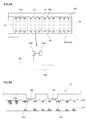
- FIG. 1A is a cross-sectional view of a light source unit including the joined body of the first embodiment
- FIG. 1B is a plan view of the joined body shown in FIG. 1A
- 2A is a partially enlarged cross-sectional view of the joined body of FIG. 1
- FIG. 2B is a view for explaining a bonding relationship between the first member, the molecular adhesive layer, and the second member.
- 3A to 3D are views for explaining a method of manufacturing a joined body. It is a figure explaining joining by electric heating.
- 5A is a perspective view of a light source unit including the joined body of the second embodiment
- FIG. 5B is a cross-sectional view of the joined body shown in FIG. 5A
- FIG. 5A is a perspective view of a light source unit including the joined body of the second embodiment
- FIG. 5B is a cross-sectional view of the joined body shown in FIG. 5A
- FIG. 5A is a perspective view of a light source unit including the joined body of
- FIG. 5C is a cross-sectional view of the light source unit of FIG. It is a figure explaining a modification.
- 6A is a diagram for explaining an electric heating portion and the like in the light source unit shown in FIG. 5A and the like
- FIG. 6B is a partially enlarged side sectional view of the portion shown in FIG. 6A.
- FIG. FIG. 8A is a diagram for explaining an electric heating portion and the like in the light source unit including the joined body of the third embodiment
- FIG. 8B is an enlarged side sectional view of a portion shown in FIG. 8A.
- FIG. 10 It is sectional drawing of the light source unit containing the conjugate
- the joined body 100 includes an optical element 10 that is a first member and a substrate 20 that is a second member.
- the optical element 10 and the substrate 20 are stacked and joined in the Z-axis direction perpendicular to the XY plane.
- the joined body 100 can be used as the light source unit 200 by providing the light emitting element 22 on the substrate 20, for example.
- the optical element (first member) 10 is a member having optical transparency that can transmit light in a wavelength range to be used.
- the optical element (first member) 10 is a transparent member when transmitting light having a wavelength in the visible light region.
- the optical element 10 is formed of a thermoplastic resin that is an organic substance.
- the thermoplastic resin is one that melts by electricity, that is, electric heat.
- COP cycloolefin polymer
- PMMA acrylic
- PC polycarbonate
- the optical element 10 has a substantially circular outline when viewed from the optical axis OA direction.
- the optical element 10 includes a lens element 10a and a support portion 10b that supports the lens element 10a from the periphery.
- the lens element 10a is a biconvex aspheric lens, for example, and has a first optical surface 11a and a second optical surface 11b.
- the support portion 10b has a flat plate portion 12a and an annular frame portion 12b extending in parallel with the optical axis OA from the outer periphery of the flat plate portion 12a.
- a protrusion 12d is formed on the end surface 12c of the frame portion 12b on the substrate 20 side.
- the protrusion 12d is formed at a portion where the optical element 10 and the substrate 20 are to be joined.
- the protrusion 12d has a double annular shape.
- the arrangement of the protrusion 12d corresponds to the wiring shape of the electric heating unit 90 described later.
- the protrusion 12d before joining has a flat surface at the tip so as to be stable when brought into contact with the electric heating part 90.
- the cross-sectional shape of the protrusion 12d is not limited to the trapezoid as shown in FIG. 3A, and may be a shape obtained by cutting out a hemisphere or an ellipse, for example.
- the optical element 10 is used as a condensing lens, for example.
- the substrate (second member) 20 is a transparent and light-transmitting plate-like member, and is a glass substrate formed of glass that is an inorganic substance.
- the optical element 10 is bonded to the first surface 20 a of the substrate 20.
- the light emitting element 22 is provided on the second surface 20 b of the substrate 20.
- the center of the light emitting element 22 is disposed on the optical axis OA of the optical element 10.
- the light emitting element 22 for example, an organic EL or LED element is used.
- a surface treatment for activating molecules is performed on the first surface 20 a that is a surface facing the optical element 10 in advance.
- the surface treatment is performed on a part or the whole of the first surface 20a.
- the surface treatment for example, corona treatment, plasma treatment, ozone treatment, and ultraviolet (UV) treatment are performed.
- the coupling force between the optical element 10 and the substrate 20 can be further increased.
- the end surface 12c of the frame portion 12b of the optical element 10 (particularly, the tip of the protrusion 12d) may be subjected to a surface treatment that activates molecules.
- the bonding strength can be further increased.
- the substrate 20 and the optical element 10 may not be subjected to the above surface treatment, and may be simply wiped and cleaned with isopropyl alcohol (IPA) or the like.
- IPA isopropyl alcohol
- a molecular adhesive layer 30 is provided between the optical element 10 and the substrate 20, specifically, on the first surface 20 a of the substrate 20.
- the molecular adhesive layer 30 may be provided at a position corresponding to the frame portion 12 b of the optical element 10, or may be provided on the entire first surface 20 a of the substrate 20.
- the molecular adhesive layer 30 is composed of a single adhesive that is covalently bonded to both the optical element 10 and the substrate 20, and basically does not include other adhesive members.
- the molecular adhesive layer 30 is illustrated as having a thickness, but in reality, the molecular adhesive layer 30 has a molecular size, and the curing shrinkage of the adhesive is taken into consideration. There is no need. As shown in FIG.
- the substrate 20 and the molecular adhesive layer 30 are formed by bonding a hydrolyzable group of the molecular adhesive through a covalent bond G1 through a hydrolysis reaction and a condensation reaction, and the optical element 10 and the molecular adhesive layer. 30, an organic functional group of the molecular adhesive is bonded by a covalent bond G2 through a predetermined reaction. Since the bonded body 100 is covalently bonded (chemically bonded) to both the optical element 10 and the substrate 20, the environment resistance is good.
- a silanol-containing adhesive or the like specifically, a silane coupling agent or the like is used as the molecular adhesive that forms the molecular adhesive layer 30, for example, a silanol-containing adhesive or the like, specifically, a silane coupling agent or the like is used.
- an electric heating section 90 is disposed at or near the boundary between the first surface 20a of the substrate 20 and the frame portion 12b of the optical element 10.
- the electrothermal unit 90 is provided at a portion where the optical element 10 and the substrate 20 are to be joined.
- the electric heating part 90 is formed of a wiring-like electric heating wire 91.
- the heating wire 91 for example, an inexpensive nichrome wire or the like is used, and the optical element 10 as the first member can be heated and melted to be bonded at a low cost.
- the heating section 90 has a double annular shape (including an inner heating wire 91a and an outer heating wire 91b).
- the arrangement of the electric heating unit 90 is not limited to an annular shape, and may be, for example, a linear shape in a direction perpendicular to the optical axis OA as long as the arrangement does not hinder wiring.
- the optical element 10 and the substrate 20 are chemically bonded via a molecular adhesive layer 30. As shown in an enlarged view in FIG. 2A, the portion where the protrusion 12d of the optical element 10 is in contact with the electric heating portion 90 and the periphery thereof are melted by the heat from the electric heating portion 90, and the melting mark is the molten portion. 12 h is a portion where the optical element 10 and the substrate 20 are locally joined.
- the optical element 10 is bonded to the substrate 20 at the position of the protrusion 12d via the molecular adhesive layer 30 by locally melting using electric heat. That is, the optical element 10 and the substrate 20 are bonded only to the portions to be bonded. Heat is generated at the bonding interface between the optical element 10 and the substrate 20 due to the heat from the electric heating portion, and the resin is melted, whereby the molecular adhesive layer 30 chemically reacts and chemically reacts with the optical element 10 and the substrate 20. To join.
- the optical element 10 as the first member is molded.
- injection molding, molding, or the like is used.
- a protrusion 12d is formed on the end surface 12c of the frame portion 12b of the optical element 10.
- the resin is melted and the heating wire 91 of the heating part 90 is attached.
- the optical element 10 is placed on the electrothermal portion 90 while positioning the optical element 10 in a state where the heating wire 91 of the electrothermal portion 90 is temporarily fixed to the transfer substrate 99a with the adhesive 99b.
- the protruding portion 12d is melted by the heat from the electric heating portion 90, and the electric heating portion 90 is embedded at the tip of the protruding portion 12d.
- the heating unit 90 may be disposed on the substrate 20.
- the heating unit 90 may be fixed on the substrate 20 using the adhesive 99 b while the heating wire 91 is pulled, or the heating wire 91 may be energized to attach the substrate 20. It may be partially melted and fixed on the substrate 20 or may be fixed integrally when the substrate 20 is manufactured.
- a substrate 20 as a second member is prepared.
- a surface treatment for activating molecules is performed on the first surface 20 a of the substrate 20. Specifically, corona treatment, plasma treatment, ozone treatment, ultraviolet (UV) treatment, or the like is performed.
- a molecular adhesive is applied to the first surface 20 a to form the molecular adhesive layer 30.
- a silane coupling agent is dissolved in water, an organic solvent, or the like, applied to a predetermined portion of the first surface 20a of the substrate 20 by a method such as dipping, spraying, or spin coating, and dried.
- the light emitting element 22 is attached to the second surface 20b of the substrate 20 (see FIG. 1A).
- the surface treatment for activating molecules may be performed on the first surface 20a before the formation of the molecular adhesive layer 30 as described above, or may be performed after the formation.
- the surface treatment can be performed on the surface of the molecular adhesive layer 30, or the surface treatment can be performed on the tip surface of the protrusion 12 d or the like.
- the power supply device 60 is used for joining (see FIG. 4).
- the substrate 20 is fixed on the support base 61.
- the substrate 20 and the optical element 10 are aligned.
- the optical element 10 may be fixed from the side surface in a state where the optical element 10 is positioned on the first surface 20 a of the substrate 20.
- the pressing device 62 is pressed against the end surface 10 s of the optical element 10 from the direction of the optical axis OA.
- the force pressed from the direction of the optical axis OA is, for example, 1N to 10N.
- the voltage of the power supply device 60 is, for example, 0.5 V to 8 V, the current is, for example, 0.1 A to 2 A, and the junction time is, for example, 0.1 seconds to 3 seconds.
- the protrusion 12 d of the optical element 10 is first in contact with the substrate 20.
- FIGS. 3C and 4 by operating the power supply device 60, heat is generated at the bonding interface between the optical element 10 and the substrate 20 (specifically, the tip of the protrusion 12 d and its periphery).
- FIG. 3D the resin at the tip of the protrusion 12d of the optical element 10 is melted.
- thermoplastic resin of the optical element 10 the glass of the substrate 20, and the silane coupling agent which is the molecular adhesive layer 30 chemically react, and these are chemically bonded. Since the melting of the resin occurs at the portion in contact with the substrate 20, only the portion of the protruding portion 12d is locally bonded. Since the contact portion between the optical element 10 and the substrate 20 is local, only a small amount of resin is melted at the protrusion 12d, and the thermal influence during shrinkage and melting is very small. By finishing the electric heating and cooling, the joined body 100 or the light source unit 200 in which the optical element 10 and the substrate 20 are joined is completed.
- a series of steps of surface treatment, formation of the molecular adhesive layer 30 and bonding by electric heating may be performed in the same atmosphere (for example, in an inert atmosphere), and the effect of the surface treatment is not lost. , It does not have to be performed in the same atmosphere.
- the heating wire 91 of the heating part 90 may be pulled out and removed, or the heating wire 91 may be left to improve the rigidity of the joined body.
- the different members (the optical element 10 as the first member) and the thermoplastic resin and the inorganic substance by chemical bonding (specifically, covalent bonding) using the molecular adhesive layer 30, and The board
- the molecular adhesive layer 30 is covalently bonded, shrinkage or the like does not occur at the time of curing as compared with an adhesive layer that is not covalently bonded, and the positional deviation between the optical element 10 and the substrate 20 can be prevented. it can.
- the bonding through the molecular adhesive layer 30 does not need to be fixed until the curing reaction is completed as in the case of an adhesive layer that is not covalently bonded, and can be relatively set by appropriately setting conditions such as a bonding temperature and a cooling method. It can be done in a short time.
- the optical element 10 and the substrate 20 are bonded using electric heat, the target location can be bonded locally (or selectively).
- the amount of thermoplastic resin that melts during bonding is very small, the amount of shrinkage of the melted resin is much smaller than the amount of shrinkage that occurs when the liquid adhesive is cured as a whole. The impact is very small. For this reason, it is difficult to affect the positional deviation between the optical element 10 and the substrate 20.
- the bonding state is good because the resin is melted using electric heat. It becomes. That is, the optical element 10 and the substrate 20 can be joined regardless of the color, and both are not limited to transparent members, and for example, a black member may be used.
- the bonding performed by melting the resin and passing through the molecular adhesive layer 30 is suitable for bonding members that have light transmission properties, dislike distortion, and have environmental resistance, particularly those that are highly important with respect to displacement.
- the bonding performed by melting the resin and passing through the molecular adhesive layer 30 is suitable for bonding members that have light transmission properties, dislike distortion, and have environmental resistance, particularly those that are highly important with respect to displacement.
- a good joined state can be achieved even in the joined body 100 in which the optical element 10 that is the first member made of resin and the substrate 20 that is the second member made of glass are combined.
- Example 1 Hereinafter, Example 1 of the present embodiment will be described.
- the first member was molded by injection molding using a thermoplastic resin as a sample.
- the first member is not an optical element but a quadrangular prism-shaped member.
- the cross section of the protrusion was trapezoidal, and the dimensions were 1 mm in height, 1.5 mm in width on the base side, 0.5 mm in width on the tip side, and 5 mm in length.
- the protrusions are formed in two rows, and the distance between the tips of the two protrusions is 3 mm.
- Thermoplastic resins include cycloolefin polymer (COP) (ZEONEX E48R (manufactured by ZEONEX)), polycarbonate (PC) (PC1600 (manufactured by Takiron)), and acrylic (PMMA) (Delagrass K (manufactured by Asahi Kasei Technoplus)) Was used.
- COP cycloolefin polymer
- PC polycarbonate
- PMMA acrylic
- Delagrass K manufactured by Asahi Kasei Technoplus
- the UV ozone cleaning was performed under the conditions that the UV wavelength (185 to 253 nm), the irradiation distance was 10 mm, and the cleaning time was 5 minutes. Plasma cleaning was performed under the conditions of a pressure of 10 Pa, an output of 150 W, and a cleaning time of 10 seconds.
- numerator wiped and cleaned the 1st surface with IPA. After the treatment, a molecular adhesive was applied to the first surface of the second member to form a molecular adhesive layer.
- silanol-containing adhesive silanol-containing adhesive (silane coupling agent SZ-6300 (manufactured by Toray Dow Corning) or silane coupling agent Z-6011 (manufactured by Toray Dow Corning)) was used. Then, the 1st member and the 2nd member were joined by electric heating, and the joined object was produced. Joining was performed under the conditions of a voltage of 8 V, a current of 2 A, a load of 10 N during joining, and a joining time of 3 seconds.
- Table 1 shows the joined state of the first member and the second member.
- silane coupling agent SZ-6300 is indicated as “A”
- silane coupling agent Z-6011 is indicated as “B”.
- the evaluation of the joined state of the joined body was judged by the joining force at the time of peeling or breaking of the first and second members. The bonding force was measured using a pull gauge, with the second member fixed, the first member chucked using a jig, pulled up vertically.
- the joined body according to the second embodiment will be described. Note that the joined body according to the second embodiment is obtained by partially changing the joined body according to the first embodiment, and matters that are not particularly described are the same as those in the first embodiment.
- a plurality of optical elements 10 as first members are locally bonded to a substrate 20 as a second member via a molecular adhesive layer 30.
- a light shield 40 is provided between the substrate 20 and the optical element 10.
- the light source unit 200 including the joined body 100 is used for a print head or the like, for example.
- the optical element 10 has a rectangular outline when viewed from the direction of the optical axis OA.
- the optical element 10 includes a plurality of lens elements 10a and a support portion 10b that supports the plurality of lens elements 10a from the periphery.
- the lens elements 10a are provided in an array.
- the support portion 10b includes a frame portion 12b extending in a direction perpendicular to the flat plate portion 12a from two opposing sides of the flat plate portion 12a.
- a protrusion 12d is formed on the end surface 12c of the frame portion 12b.
- the electrothermal unit 90 is an electrothermal wiring 93 formed on an electrothermal sheet 92.
- the electrothermal sheet 92 is a frame-shaped thin film provided between the optical element 10 and the substrate 20. That is, the electrothermal sheet 92 is provided at a position corresponding to the frame portion 12b (see FIG. 5B) of the optical element 10, and is not provided at a position corresponding to the lens element 10a. Fine holes 92a are partially formed in the electric heating sheet 92. When the resin of the optical element 10 is melted, the molten resin passes through the holes 92a of the electric heating sheet 92, and the molecular adhesive layer 30.
- the entire electrothermal sheet 92 may be mesh.
- the electric heating wiring 93 is formed so as to correspond to the position of the protrusion 12 d of the optical element 10.
- the electric heating wire 93 may be formed by embedding an electric heating wire in the electric heating sheet 92.
- the electric heating sheet 92 has a mesh shape, it may be formed by printing a metal wiring pattern.
- a plurality of light emitting elements 22 are provided in an array on the second surface 20 b of the substrate 20 at positions corresponding to the lens elements 10 a of the optical element 10.
- the light shield 40 is a flat plate member that shields unnecessary light from the light emitting element 22.
- the light shielding body 40 for example, a glass or resin substrate containing light-absorbing particles such as black, a metal substrate painted black, or the like is used.
- An opening 40 a is formed in the light shielding body 40 at a position corresponding to the lens element 10 a of the optical element 10.
- the light shield 40 is bonded to the substrate 20 side.
- the light blocking body 40 may be bonded with an adhesive other than a molecular adhesive, but may be bonded using electric heat in the same manner as the bonding between the optical element 10 and the substrate 20 depending on the combination of materials. For example, if the material of the light shielding body 40 is a resin different from the inorganic material that is the material of the substrate 20, the light shielding body 40 can be bonded via the molecular adhesive layer 130.
- the plurality of optical elements 10 may be bonded together by electric heating in a state where all the optical elements 10 are arranged on the first surface 20 a of the substrate 20, or the optical elements 10 are arranged in units of one or several. You may make it join in several times by electroheating.
- joining by electric heating can be performed in a relatively short time as long as the wattage is high, so that a plurality of optical elements (first members) 10 are joined at once or divided into a plurality of times. Even if it makes it, it can join in a comparatively short time and productivity is good.
- the electric heating wiring 93 is formed on the electric heating sheet 92, the shape of the electric heating portion 90 is stable and easy to assemble. Thereby, the part to be melted of the optical element 10 can be melted with high accuracy. Moreover, since the process of directly patterning a heating wire on the optical element 10 or the substrate 20 is not required, the production efficiency is good.
- the light source unit 200 including the joined body 100 is provided, for example, in an image forming unit 80 built in an electrophotographic printer that is an image forming apparatus.
- the image forming unit 80 is for transferring development toner onto a sheet.
- the image forming unit 80 includes a photoconductor 81, a charging roller 82, a print head 83, a developing device 84, a transfer device 85, a cleaning device 86, and a charge eliminating device 87.
- the light source unit 200 is provided in the print head 83 among these.
- the other members 82 to 87 act on the photosensitive member 81, whereby an image is formed on the paper PP.
- the light blocking body 40 is not limited to being bonded to the substrate 20 side, but may be bonded to the optical element 10 side. In this case, even if the material of the light blocking body 40 is any of resin, glass, and metal, it can be bonded via the molecular adhesive layer 230.
- the joined body according to the third embodiment will be described. Note that the joined body according to the third embodiment is obtained by partially changing the joined body according to the second embodiment, and matters that are not particularly described are the same as those in the second embodiment.
- the electrothermal unit 90 is a wiring pattern 95.
- the wiring pattern 95 is formed by printing a metal wiring pattern.
- a wiring pattern 95 is formed on the surface (first surface 20 a) of the substrate 20.
- the wiring pattern 95 is disposed so as to correspond to the position of the protrusion 12d of the optical element 10.
- the electrothermal unit 90 may be provided on the optical element 10 side.
- the wiring pattern 95 is about several ⁇ m, only a finer part can be melted.
- the thickness of the electric heating section 90 can be made relatively thin, the amount of melting of the resin can be made relatively smaller than that of the heating wire, and the melting time can also be made relatively short.
- the joined body according to the fourth embodiment will be described. Note that the joined body according to the fourth embodiment is obtained by partially changing the joined body according to the first embodiment, and items that are not particularly described are the same as those in the first embodiment.
- the joined body 100 includes an optical element 50 as a third member in addition to the optical element 10 as a first member and the substrate 20 as a second member.
- the optical element 50 is overlapped and bonded on the optical element 10. That is, the optical element 50 is further bonded to the optical element 10 to which the substrate 20 is bonded.
- the optical element 50 is a transparent and light-transmitting member, and is formed of a thermoplastic resin that is an organic substance.
- the shape of the optical element 50 is the same as the shape of the optical element 10, but can be changed as appropriate.
- the optical element 50 includes a lens element 50a and a support portion 50b that supports the lens element 50a from the periphery.
- the lens element 50a is, for example, a biconvex aspheric lens, and has a third optical surface 51a and a fourth optical surface 51b.
- the support portion 50b includes a flat plate portion 52a and an annular frame portion 52b extending from the flat plate portion 52a in parallel with the optical axis OA.
- a protrusion 52d is formed on the end surface 52c of the frame portion 52b on the optical element 10 side.
- an electric heating unit 190 is provided between the optical element 10 and the optical element 50. That is, the wiring-shaped electrothermal portion 190 is disposed at or near the boundary between the optical element (third member) 50 and the optical element (first member) 10.
- the protrusion 52d of the optical element 50 and the support part 10b of the optical element 10 are interposed via the molecular adhesive layer 330 by locally melting with electric heating. Are locally chemically bonded. Thereby, the joined body 100 in which the two optical elements 10 and 50 are stacked on the substrate 20 can be obtained.
- a plurality of optical elements 10 and 50 may be arranged on one substrate 20 as in the second embodiment.
- the joined body according to the fifth embodiment will be described. Note that the joined body according to the fifth embodiment is obtained by partially changing the joined body of the first or second embodiment, and matters that are not particularly described are the same as those in the first or second embodiment.
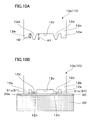
- a leg portion 12e is formed on the end surface 12c of the frame portion 12b on the substrate 20 side in addition to the protruding portion 12d.
- the protrusion 12d is provided in a state sandwiched between the legs 12e, and as shown in FIG. 10A, the height H1 of the protrusion 12d is higher than the height H2 of the legs 12e before joining. .
- the protruding portion 12d has substantially the same height as the leg portion 12e in the melted state. At the time of joining, if the projection 12d is melted using electric heat and the heating is terminated when the leg 12e comes into contact with the substrate 20, the optical element 10 is more stably supported by the leg 12e. Become.
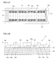
- legs 12e may be provided so as to be sandwiched between each pair of protrusions 12d as shown in FIGS. 11A and 11B.
- the position of the leg part 12e can be changed suitably, for example, you may provide the leg part 12e also between the lens elements 10a.
- the lens element 10a has a light guide 11g on the substrate 20 side instead of the second optical surface 11b in the first embodiment.
- the light guide portion 11g is columnar and has a flat surface 11c at the lower end.
- the light guide portion 11g may be cylindrical or prismatic, and may or may not have a taper.
- a light shielding part 11r is formed on the side surface of the light guide part 11g to prevent intrusion of external light.
- the light shielding part 11r is formed, for example, by attaching a black light shielding film, forming a black light shielding film, or applying a texture.
- the light guide 11g corresponds to each lens element 10a. When the light emitting element 22 emits light in the light source unit 200 including the joined body 100, the light passes through the substrate 20, the light guide 11g, and the lens element 10a. Then, the light is emitted from the first optical surface 11a to form an image.
- a projection 12d is provided on the end surface 12c of the frame portion 12b of the optical element 10.
- the flat surface 11c of the light guide portion 11g comes into contact with the substrate 20 in a state where the projection 12d is melted using electric heat and the optical element 10 and the substrate 20 are joined.
- a plurality of optical elements 10 may be arranged on one substrate 20 as in the second embodiment.
- the joined body according to the seventh embodiment will be described.
- the joined body according to the seventh embodiment is obtained by partially changing the joined body according to the sixth embodiment, and matters that are not particularly described are the same as those in the sixth embodiment.
- the liquid LQ is sealed in a sealed space formed between the optical element 10 that is the first member and the substrate 20 that is the second member.
- a liquid resin a material without an ultraviolet curing or thermosetting initiator
- oil or the like is used.
- the lens element 10a has a light guide portion 11g on the substrate 20 side instead of the second optical surface 11b in the first embodiment.
- 11 g of light guides are columnar, and have the recessed part 11k for filling the liquid LQ in a lower end part.
- a protrusion 11p is provided on the outer peripheral portion 11m of the light guide portion 11g.
- a light shielding part 11r is formed on the side surface of the light guide part 11g to prevent intrusion of external light.
- the liquid LQ is filled in the recess 11k before bonding, and these are bonded in a state where the liquid LQ is sandwiched between the optical element 10 and the substrate 20.
- the substrate 20 is plate-shaped, and if the joint surface between the optical element 10 and the substrate 20 is large, the substrate 20 may be warped. Therefore, it is possible to prevent the optical path from being obstructed by reflection loss by limiting the joint surface to the outer periphery and enclosing, for example, liquid LQ having a refractive index equivalent to that of the optical element 10 inside.
- a plurality of optical elements 10 may be arranged on one substrate 20 as in the second embodiment.
- the joined body etc. which concern on embodiment were demonstrated, the joined body etc. which concern on this invention are not restricted to said thing.
- the shape and size of the optical elements 10 and 50 can be changed as appropriate according to the application and function.
- the first member and the second member are not limited to the optical element 10 and the substrate 20, respectively, and can be appropriately changed according to the application.
- the optical element 10 may be provided with the protrusions 12d and 11p, and the resin around the electric heating portion 90 may be melted and bonded.
- the optical element 10 is not limited to an array-shaped optical element, and may be one as in the first embodiment.
- a plurality of optical elements 10 having lens elements 10a may be arranged, or a plurality of stacked optical elements 10 and 50 as in the third embodiment may be arranged.
- the joined body 100 of the second embodiment may be cut into individual pieces.
Landscapes
- Engineering & Computer Science (AREA)
- Mechanical Engineering (AREA)
- Lining Or Joining Of Plastics Or The Like (AREA)
- Mounting And Adjusting Of Optical Elements (AREA)
Abstract
La présente invention concerne un corps lié comprenant : un élément optique (10) qui est un premier élément formé à partir d'une résine thermoplastique ; et un substrat (20) qui est un second élément formé à partir d'un matériau inorganique. Le corps lié comprend une couche adhésive moléculaire (30) entre l'élément optique (10) et le substrat (20). L'élément optique (10) est chimiquement lié au substrat (20) via la couche adhésive moléculaire (30) par fusion localement avec de la chaleur provenant d'une unité de chauffage électrique (90) de type câble disposée à la limite ou à proximité de la limite entre l'élément optique (10) et le substrat (20).
Priority Applications (1)
| Application Number | Priority Date | Filing Date | Title |
|---|---|---|---|
| JP2017526459A JPWO2017002973A1 (ja) | 2015-07-02 | 2016-07-01 | 接合体及び接合体の製造方法 |
Applications Claiming Priority (2)
| Application Number | Priority Date | Filing Date | Title |
|---|---|---|---|
| JP2015-133978 | 2015-07-02 | ||
| JP2015133978 | 2015-07-02 |
Publications (1)
| Publication Number | Publication Date |
|---|---|
| WO2017002973A1 true WO2017002973A1 (fr) | 2017-01-05 |
Family
ID=57608309
Family Applications (1)
| Application Number | Title | Priority Date | Filing Date |
|---|---|---|---|
| PCT/JP2016/069716 WO2017002973A1 (fr) | 2015-07-02 | 2016-07-01 | Corps lié et procédé de production d'un corps lié |
Country Status (2)
| Country | Link |
|---|---|
| JP (1) | JPWO2017002973A1 (fr) |
| WO (1) | WO2017002973A1 (fr) |
Citations (7)
| Publication number | Priority date | Publication date | Assignee | Title |
|---|---|---|---|---|
| JPS612738A (ja) * | 1984-06-13 | 1986-01-08 | Sumitomo Electric Ind Ltd | 合成樹脂成形品の表面処理方法 |
| JPH0557797A (ja) * | 1990-12-29 | 1993-03-09 | Asahi Glass Co Ltd | 樹脂枠体付きガラス窓の製造法 |
| JP2003181932A (ja) * | 2001-12-21 | 2003-07-03 | Asahi Kasei Corp | 成形品の接合方法 |
| JP2004133073A (ja) * | 2002-10-09 | 2004-04-30 | Canon Inc | 光学部材の固定構造、および光学ユニット |
| JP2007237519A (ja) * | 2006-03-07 | 2007-09-20 | Yokohama Rubber Co Ltd:The | 樹脂集積配管の製造方法および樹脂集積配管 |
| JP2008284782A (ja) * | 2007-05-17 | 2008-11-27 | Hamamatsu Photonics Kk | 樹脂・ガラス溶着方法及び樹脂・ガラス溶着装置 |
| WO2011010738A1 (fr) * | 2009-07-24 | 2011-01-27 | Taga Yasunori | Procédé de production dune structure dassemblage et structure dassemblage |
-
2016
- 2016-07-01 JP JP2017526459A patent/JPWO2017002973A1/ja active Pending
- 2016-07-01 WO PCT/JP2016/069716 patent/WO2017002973A1/fr active Application Filing
Patent Citations (7)
| Publication number | Priority date | Publication date | Assignee | Title |
|---|---|---|---|---|
| JPS612738A (ja) * | 1984-06-13 | 1986-01-08 | Sumitomo Electric Ind Ltd | 合成樹脂成形品の表面処理方法 |
| JPH0557797A (ja) * | 1990-12-29 | 1993-03-09 | Asahi Glass Co Ltd | 樹脂枠体付きガラス窓の製造法 |
| JP2003181932A (ja) * | 2001-12-21 | 2003-07-03 | Asahi Kasei Corp | 成形品の接合方法 |
| JP2004133073A (ja) * | 2002-10-09 | 2004-04-30 | Canon Inc | 光学部材の固定構造、および光学ユニット |
| JP2007237519A (ja) * | 2006-03-07 | 2007-09-20 | Yokohama Rubber Co Ltd:The | 樹脂集積配管の製造方法および樹脂集積配管 |
| JP2008284782A (ja) * | 2007-05-17 | 2008-11-27 | Hamamatsu Photonics Kk | 樹脂・ガラス溶着方法及び樹脂・ガラス溶着装置 |
| WO2011010738A1 (fr) * | 2009-07-24 | 2011-01-27 | Taga Yasunori | Procédé de production dune structure dassemblage et structure dassemblage |
Also Published As
| Publication number | Publication date |
|---|---|
| JPWO2017002973A1 (ja) | 2018-04-12 |
Similar Documents
| Publication | Publication Date | Title |
|---|---|---|
| TWI298804B (en) | Method of fixing optical member and optical unit | |
| KR102131962B1 (ko) | 커버 윈도우의 제조장치 및 커버 윈도우의 제조방법 | |
| JP6173354B2 (ja) | 光透過型インプリント用モールド、大面積モールドの製造方法 | |
| JP5498219B2 (ja) | ミラー面を有する光導波路の製造方法及び光電複合配線板 | |
| JP6567969B2 (ja) | 三次元複雑多層構造物及びその製造方法 | |
| JP4071187B2 (ja) | 光学デバイスおよびその作製方法 | |
| JPWO2007007755A1 (ja) | 反射防止構造体を備えた光学機器の製造方法 | |
| TW201040600A (en) | Method of manufacturing optical waveguide core, method of manufacturing optical waveguide, optical waveguide, and optoelectric composite wiring board | |
| TWI464027B (zh) | 利用雷射光之部件分離方法 | |
| WO2017002974A1 (fr) | Corps lié et procédé de production d'un corps lié | |
| US8790483B2 (en) | Method of weldbonding and a device comprising weldbonded components | |
| WO2017002973A1 (fr) | Corps lié et procédé de production d'un corps lié | |
| WO2013147105A1 (fr) | Moule en forme de rouleau et procédé permettant de fabriquer un moule en forme de rouleau ainsi qu'un élément | |
| US9229558B2 (en) | Method of manufacturing touch panel and touch panel | |
| JP2010271465A (ja) | 遮光膜付マイクロレンズアレイの製造方法、製造装置、及び遮光膜付マイクロレンズアレイ | |
| JP2007240583A (ja) | レンズユニットおよびその製造方法 | |
| JP4498127B2 (ja) | 光学部材固定方法および光学機器 | |
| JP2014040061A (ja) | マイクロ流路チップの製造方法及びマイクロ流路チップ | |
| CN108472877B (zh) | 接合体的制造方法 | |
| JP2016048357A (ja) | 曲面スクリーンを構成する積層体の製造方法 | |
| US20220384674A1 (en) | Method of manufacturing electric device | |
| JP3718218B2 (ja) | フィルムスクリーンの製造装置及び製造方法 | |
| KR20110132523A (ko) | 광 도파로의 제조 방법 | |
| JP2011032144A (ja) | ガラス製部材の接着方法及びガラス製部材の接合体 | |
| JP2005088444A (ja) | 光透過性スタンパの製造方法及び光メモリ素子の製造方法 |
Legal Events
| Date | Code | Title | Description |
|---|---|---|---|
| 121 | Ep: the epo has been informed by wipo that ep was designated in this application |
Ref document number: 16818081 Country of ref document: EP Kind code of ref document: A1 |
|
| ENP | Entry into the national phase |
Ref document number: 2017526459 Country of ref document: JP Kind code of ref document: A |
|
| NENP | Non-entry into the national phase |
Ref country code: DE |
|
| 122 | Ep: pct application non-entry in european phase |
Ref document number: 16818081 Country of ref document: EP Kind code of ref document: A1 |