WO2017002973A1 - Bonded body and method for producing bonded body - Google Patents
Bonded body and method for producing bonded body Download PDFInfo
- Publication number
- WO2017002973A1 WO2017002973A1 PCT/JP2016/069716 JP2016069716W WO2017002973A1 WO 2017002973 A1 WO2017002973 A1 WO 2017002973A1 JP 2016069716 W JP2016069716 W JP 2016069716W WO 2017002973 A1 WO2017002973 A1 WO 2017002973A1
- Authority
- WO
- WIPO (PCT)
- Prior art keywords
- joined body
- optical element
- substrate
- adhesive layer
- body according
- Prior art date
Links
Images


Classifications
-
- B—PERFORMING OPERATIONS; TRANSPORTING
- B29—WORKING OF PLASTICS; WORKING OF SUBSTANCES IN A PLASTIC STATE IN GENERAL
- B29C—SHAPING OR JOINING OF PLASTICS; SHAPING OF MATERIAL IN A PLASTIC STATE, NOT OTHERWISE PROVIDED FOR; AFTER-TREATMENT OF THE SHAPED PRODUCTS, e.g. REPAIRING
- B29C65/00—Joining or sealing of preformed parts, e.g. welding of plastics materials; Apparatus therefor
- B29C65/02—Joining or sealing of preformed parts, e.g. welding of plastics materials; Apparatus therefor by heating, with or without pressure
Definitions
- the present invention relates to a joined body composed of a thermoplastic resin and an inorganic material and a method for producing the joined body.
- the environmental resistance of the joining material (specifically, resin or primer).
- the environmental resistance of the joining material (specifically, resin or primer).
- the bonding material may swell and peel off.
- the hygroscopicity of the bonded portion is low, the bonded material cannot be fully endured and the bonded material may be destroyed.
- methods such as Patent Documents 1 and 2 that are pressure-bonded on the surface are suitable for joining sheets and films. It is difficult to join.
- Patent Document 3 is limited to bonding of a material that absorbs laser light and a material that transmits laser light, and for example, it is difficult to bond transparent members or black members.
- An object of the present invention is to provide a bonded body in which different members such as a thermoplastic resin and an inorganic material are partially bonded and in a good bonded state.
- the present invention also aims to provide a method for producing this type of joined body.
- a joined body includes a first member formed of a thermoplastic resin and a second member formed of an inorganic material, and the first member is interposed between the first member and the second member.
- the molecular adhesive layer has a molecular adhesive layer, and the first member is locally melted by heat from a wiring-shaped electrothermal portion disposed at or near the boundary between the first and second members. It is chemically joined to the 2nd member via.
- the molecular adhesive layer is composed of a single adhesive that is covalently bonded to both the first and second members, and basically does not include other adhesive members.
- different members such as a thermoplastic resin and an inorganic material can be joined by chemical bonding (specifically, covalent bonding) using a molecular adhesive layer.
- the molecular adhesive is basically not mixed with other bonding members, for example, as in the case where the molecular adhesive is substantially composed of only the silane coupling agent, a stable bonding force can be obtained.
- the molecular adhesive layer is covalently bonded, shrinkage or the like does not occur at the time of curing as compared with an adhesive layer that is not covalently bonded, and positional displacement between the first and second members can be prevented.
- the bonding through the molecular adhesive layer does not need to be fixed until the curing reaction is completed unlike the adhesive layer that is not covalently bonded, and is relatively short by appropriately setting conditions such as the bonding temperature and the cooling method. Can be done in time.
- the target location can be joined locally (or selectively). Since the amount of thermoplastic resin that melts during bonding is very small, the amount of shrinkage of the melted resin is much smaller than the amount of shrinkage that occurs when the liquid adhesive is cured as a whole. The impact is very small. Therefore, it is difficult to affect the positional deviation between the first and second members.
- a wiring-shaped electrothermal portion is provided at or near the boundary between the first member formed of a thermoplastic resin and the second member formed of an inorganic substance, and the second member
- a molecular adhesive layer is provided on the surface facing one member, and the first member is locally melted by heat from the electric heating portion and chemically bonded to the second member through the molecular adhesive layer.
- thermoplastic resin and an inorganic substance can be stably joined by chemical bonding (covalent bonding) using a molecular adhesive layer.
- the molecular adhesive layer does not shrink during curing, and can prevent displacement between the first and second members.
- the bonding via the molecular adhesive layer can be performed in a relatively short time.
- the first and second members are joined using electric heat, they can be joined locally. Since the thermoplastic resin that melts at the time of joining is a very small amount, the thermal influence during curing shrinkage and melting is very small, and the positional deviation between the first and second members is hardly affected.
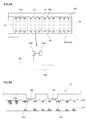
- FIG. 1A is a cross-sectional view of a light source unit including the joined body of the first embodiment
- FIG. 1B is a plan view of the joined body shown in FIG. 1A
- 2A is a partially enlarged cross-sectional view of the joined body of FIG. 1
- FIG. 2B is a view for explaining a bonding relationship between the first member, the molecular adhesive layer, and the second member.
- 3A to 3D are views for explaining a method of manufacturing a joined body. It is a figure explaining joining by electric heating.
- 5A is a perspective view of a light source unit including the joined body of the second embodiment
- FIG. 5B is a cross-sectional view of the joined body shown in FIG. 5A
- FIG. 5A is a perspective view of a light source unit including the joined body of the second embodiment
- FIG. 5B is a cross-sectional view of the joined body shown in FIG. 5A
- FIG. 5A is a perspective view of a light source unit including the joined body of
- FIG. 5C is a cross-sectional view of the light source unit of FIG. It is a figure explaining a modification.
- 6A is a diagram for explaining an electric heating portion and the like in the light source unit shown in FIG. 5A and the like
- FIG. 6B is a partially enlarged side sectional view of the portion shown in FIG. 6A.
- FIG. FIG. 8A is a diagram for explaining an electric heating portion and the like in the light source unit including the joined body of the third embodiment
- FIG. 8B is an enlarged side sectional view of a portion shown in FIG. 8A.
- FIG. 10 It is sectional drawing of the light source unit containing the conjugate
- the joined body 100 includes an optical element 10 that is a first member and a substrate 20 that is a second member.
- the optical element 10 and the substrate 20 are stacked and joined in the Z-axis direction perpendicular to the XY plane.
- the joined body 100 can be used as the light source unit 200 by providing the light emitting element 22 on the substrate 20, for example.
- the optical element (first member) 10 is a member having optical transparency that can transmit light in a wavelength range to be used.
- the optical element (first member) 10 is a transparent member when transmitting light having a wavelength in the visible light region.
- the optical element 10 is formed of a thermoplastic resin that is an organic substance.
- the thermoplastic resin is one that melts by electricity, that is, electric heat.
- COP cycloolefin polymer
- PMMA acrylic
- PC polycarbonate
- the optical element 10 has a substantially circular outline when viewed from the optical axis OA direction.
- the optical element 10 includes a lens element 10a and a support portion 10b that supports the lens element 10a from the periphery.
- the lens element 10a is a biconvex aspheric lens, for example, and has a first optical surface 11a and a second optical surface 11b.
- the support portion 10b has a flat plate portion 12a and an annular frame portion 12b extending in parallel with the optical axis OA from the outer periphery of the flat plate portion 12a.
- a protrusion 12d is formed on the end surface 12c of the frame portion 12b on the substrate 20 side.
- the protrusion 12d is formed at a portion where the optical element 10 and the substrate 20 are to be joined.
- the protrusion 12d has a double annular shape.
- the arrangement of the protrusion 12d corresponds to the wiring shape of the electric heating unit 90 described later.
- the protrusion 12d before joining has a flat surface at the tip so as to be stable when brought into contact with the electric heating part 90.
- the cross-sectional shape of the protrusion 12d is not limited to the trapezoid as shown in FIG. 3A, and may be a shape obtained by cutting out a hemisphere or an ellipse, for example.
- the optical element 10 is used as a condensing lens, for example.
- the substrate (second member) 20 is a transparent and light-transmitting plate-like member, and is a glass substrate formed of glass that is an inorganic substance.
- the optical element 10 is bonded to the first surface 20 a of the substrate 20.
- the light emitting element 22 is provided on the second surface 20 b of the substrate 20.
- the center of the light emitting element 22 is disposed on the optical axis OA of the optical element 10.
- the light emitting element 22 for example, an organic EL or LED element is used.
- a surface treatment for activating molecules is performed on the first surface 20 a that is a surface facing the optical element 10 in advance.
- the surface treatment is performed on a part or the whole of the first surface 20a.
- the surface treatment for example, corona treatment, plasma treatment, ozone treatment, and ultraviolet (UV) treatment are performed.
- the coupling force between the optical element 10 and the substrate 20 can be further increased.
- the end surface 12c of the frame portion 12b of the optical element 10 (particularly, the tip of the protrusion 12d) may be subjected to a surface treatment that activates molecules.
- the bonding strength can be further increased.
- the substrate 20 and the optical element 10 may not be subjected to the above surface treatment, and may be simply wiped and cleaned with isopropyl alcohol (IPA) or the like.
- IPA isopropyl alcohol
- a molecular adhesive layer 30 is provided between the optical element 10 and the substrate 20, specifically, on the first surface 20 a of the substrate 20.
- the molecular adhesive layer 30 may be provided at a position corresponding to the frame portion 12 b of the optical element 10, or may be provided on the entire first surface 20 a of the substrate 20.
- the molecular adhesive layer 30 is composed of a single adhesive that is covalently bonded to both the optical element 10 and the substrate 20, and basically does not include other adhesive members.
- the molecular adhesive layer 30 is illustrated as having a thickness, but in reality, the molecular adhesive layer 30 has a molecular size, and the curing shrinkage of the adhesive is taken into consideration. There is no need. As shown in FIG.
- the substrate 20 and the molecular adhesive layer 30 are formed by bonding a hydrolyzable group of the molecular adhesive through a covalent bond G1 through a hydrolysis reaction and a condensation reaction, and the optical element 10 and the molecular adhesive layer. 30, an organic functional group of the molecular adhesive is bonded by a covalent bond G2 through a predetermined reaction. Since the bonded body 100 is covalently bonded (chemically bonded) to both the optical element 10 and the substrate 20, the environment resistance is good.
- a silanol-containing adhesive or the like specifically, a silane coupling agent or the like is used as the molecular adhesive that forms the molecular adhesive layer 30, for example, a silanol-containing adhesive or the like, specifically, a silane coupling agent or the like is used.
- an electric heating section 90 is disposed at or near the boundary between the first surface 20a of the substrate 20 and the frame portion 12b of the optical element 10.
- the electrothermal unit 90 is provided at a portion where the optical element 10 and the substrate 20 are to be joined.
- the electric heating part 90 is formed of a wiring-like electric heating wire 91.
- the heating wire 91 for example, an inexpensive nichrome wire or the like is used, and the optical element 10 as the first member can be heated and melted to be bonded at a low cost.
- the heating section 90 has a double annular shape (including an inner heating wire 91a and an outer heating wire 91b).
- the arrangement of the electric heating unit 90 is not limited to an annular shape, and may be, for example, a linear shape in a direction perpendicular to the optical axis OA as long as the arrangement does not hinder wiring.
- the optical element 10 and the substrate 20 are chemically bonded via a molecular adhesive layer 30. As shown in an enlarged view in FIG. 2A, the portion where the protrusion 12d of the optical element 10 is in contact with the electric heating portion 90 and the periphery thereof are melted by the heat from the electric heating portion 90, and the melting mark is the molten portion. 12 h is a portion where the optical element 10 and the substrate 20 are locally joined.
- the optical element 10 is bonded to the substrate 20 at the position of the protrusion 12d via the molecular adhesive layer 30 by locally melting using electric heat. That is, the optical element 10 and the substrate 20 are bonded only to the portions to be bonded. Heat is generated at the bonding interface between the optical element 10 and the substrate 20 due to the heat from the electric heating portion, and the resin is melted, whereby the molecular adhesive layer 30 chemically reacts and chemically reacts with the optical element 10 and the substrate 20. To join.
- the optical element 10 as the first member is molded.
- injection molding, molding, or the like is used.
- a protrusion 12d is formed on the end surface 12c of the frame portion 12b of the optical element 10.
- the resin is melted and the heating wire 91 of the heating part 90 is attached.
- the optical element 10 is placed on the electrothermal portion 90 while positioning the optical element 10 in a state where the heating wire 91 of the electrothermal portion 90 is temporarily fixed to the transfer substrate 99a with the adhesive 99b.
- the protruding portion 12d is melted by the heat from the electric heating portion 90, and the electric heating portion 90 is embedded at the tip of the protruding portion 12d.
- the heating unit 90 may be disposed on the substrate 20.
- the heating unit 90 may be fixed on the substrate 20 using the adhesive 99 b while the heating wire 91 is pulled, or the heating wire 91 may be energized to attach the substrate 20. It may be partially melted and fixed on the substrate 20 or may be fixed integrally when the substrate 20 is manufactured.
- a substrate 20 as a second member is prepared.
- a surface treatment for activating molecules is performed on the first surface 20 a of the substrate 20. Specifically, corona treatment, plasma treatment, ozone treatment, ultraviolet (UV) treatment, or the like is performed.
- a molecular adhesive is applied to the first surface 20 a to form the molecular adhesive layer 30.
- a silane coupling agent is dissolved in water, an organic solvent, or the like, applied to a predetermined portion of the first surface 20a of the substrate 20 by a method such as dipping, spraying, or spin coating, and dried.
- the light emitting element 22 is attached to the second surface 20b of the substrate 20 (see FIG. 1A).
- the surface treatment for activating molecules may be performed on the first surface 20a before the formation of the molecular adhesive layer 30 as described above, or may be performed after the formation.
- the surface treatment can be performed on the surface of the molecular adhesive layer 30, or the surface treatment can be performed on the tip surface of the protrusion 12 d or the like.
- the power supply device 60 is used for joining (see FIG. 4).
- the substrate 20 is fixed on the support base 61.
- the substrate 20 and the optical element 10 are aligned.
- the optical element 10 may be fixed from the side surface in a state where the optical element 10 is positioned on the first surface 20 a of the substrate 20.
- the pressing device 62 is pressed against the end surface 10 s of the optical element 10 from the direction of the optical axis OA.
- the force pressed from the direction of the optical axis OA is, for example, 1N to 10N.
- the voltage of the power supply device 60 is, for example, 0.5 V to 8 V, the current is, for example, 0.1 A to 2 A, and the junction time is, for example, 0.1 seconds to 3 seconds.
- the protrusion 12 d of the optical element 10 is first in contact with the substrate 20.
- FIGS. 3C and 4 by operating the power supply device 60, heat is generated at the bonding interface between the optical element 10 and the substrate 20 (specifically, the tip of the protrusion 12 d and its periphery).
- FIG. 3D the resin at the tip of the protrusion 12d of the optical element 10 is melted.
- thermoplastic resin of the optical element 10 the glass of the substrate 20, and the silane coupling agent which is the molecular adhesive layer 30 chemically react, and these are chemically bonded. Since the melting of the resin occurs at the portion in contact with the substrate 20, only the portion of the protruding portion 12d is locally bonded. Since the contact portion between the optical element 10 and the substrate 20 is local, only a small amount of resin is melted at the protrusion 12d, and the thermal influence during shrinkage and melting is very small. By finishing the electric heating and cooling, the joined body 100 or the light source unit 200 in which the optical element 10 and the substrate 20 are joined is completed.
- a series of steps of surface treatment, formation of the molecular adhesive layer 30 and bonding by electric heating may be performed in the same atmosphere (for example, in an inert atmosphere), and the effect of the surface treatment is not lost. , It does not have to be performed in the same atmosphere.
- the heating wire 91 of the heating part 90 may be pulled out and removed, or the heating wire 91 may be left to improve the rigidity of the joined body.
- the different members (the optical element 10 as the first member) and the thermoplastic resin and the inorganic substance by chemical bonding (specifically, covalent bonding) using the molecular adhesive layer 30, and The board
- the molecular adhesive layer 30 is covalently bonded, shrinkage or the like does not occur at the time of curing as compared with an adhesive layer that is not covalently bonded, and the positional deviation between the optical element 10 and the substrate 20 can be prevented. it can.
- the bonding through the molecular adhesive layer 30 does not need to be fixed until the curing reaction is completed as in the case of an adhesive layer that is not covalently bonded, and can be relatively set by appropriately setting conditions such as a bonding temperature and a cooling method. It can be done in a short time.
- the optical element 10 and the substrate 20 are bonded using electric heat, the target location can be bonded locally (or selectively).
- the amount of thermoplastic resin that melts during bonding is very small, the amount of shrinkage of the melted resin is much smaller than the amount of shrinkage that occurs when the liquid adhesive is cured as a whole. The impact is very small. For this reason, it is difficult to affect the positional deviation between the optical element 10 and the substrate 20.
- the bonding state is good because the resin is melted using electric heat. It becomes. That is, the optical element 10 and the substrate 20 can be joined regardless of the color, and both are not limited to transparent members, and for example, a black member may be used.
- the bonding performed by melting the resin and passing through the molecular adhesive layer 30 is suitable for bonding members that have light transmission properties, dislike distortion, and have environmental resistance, particularly those that are highly important with respect to displacement.
- the bonding performed by melting the resin and passing through the molecular adhesive layer 30 is suitable for bonding members that have light transmission properties, dislike distortion, and have environmental resistance, particularly those that are highly important with respect to displacement.
- a good joined state can be achieved even in the joined body 100 in which the optical element 10 that is the first member made of resin and the substrate 20 that is the second member made of glass are combined.
- Example 1 Hereinafter, Example 1 of the present embodiment will be described.
- the first member was molded by injection molding using a thermoplastic resin as a sample.
- the first member is not an optical element but a quadrangular prism-shaped member.
- the cross section of the protrusion was trapezoidal, and the dimensions were 1 mm in height, 1.5 mm in width on the base side, 0.5 mm in width on the tip side, and 5 mm in length.
- the protrusions are formed in two rows, and the distance between the tips of the two protrusions is 3 mm.
- Thermoplastic resins include cycloolefin polymer (COP) (ZEONEX E48R (manufactured by ZEONEX)), polycarbonate (PC) (PC1600 (manufactured by Takiron)), and acrylic (PMMA) (Delagrass K (manufactured by Asahi Kasei Technoplus)) Was used.
- COP cycloolefin polymer
- PC polycarbonate
- PMMA acrylic
- Delagrass K manufactured by Asahi Kasei Technoplus
- the UV ozone cleaning was performed under the conditions that the UV wavelength (185 to 253 nm), the irradiation distance was 10 mm, and the cleaning time was 5 minutes. Plasma cleaning was performed under the conditions of a pressure of 10 Pa, an output of 150 W, and a cleaning time of 10 seconds.
- numerator wiped and cleaned the 1st surface with IPA. After the treatment, a molecular adhesive was applied to the first surface of the second member to form a molecular adhesive layer.
- silanol-containing adhesive silanol-containing adhesive (silane coupling agent SZ-6300 (manufactured by Toray Dow Corning) or silane coupling agent Z-6011 (manufactured by Toray Dow Corning)) was used. Then, the 1st member and the 2nd member were joined by electric heating, and the joined object was produced. Joining was performed under the conditions of a voltage of 8 V, a current of 2 A, a load of 10 N during joining, and a joining time of 3 seconds.
- Table 1 shows the joined state of the first member and the second member.
- silane coupling agent SZ-6300 is indicated as “A”
- silane coupling agent Z-6011 is indicated as “B”.
- the evaluation of the joined state of the joined body was judged by the joining force at the time of peeling or breaking of the first and second members. The bonding force was measured using a pull gauge, with the second member fixed, the first member chucked using a jig, pulled up vertically.
- the joined body according to the second embodiment will be described. Note that the joined body according to the second embodiment is obtained by partially changing the joined body according to the first embodiment, and matters that are not particularly described are the same as those in the first embodiment.
- a plurality of optical elements 10 as first members are locally bonded to a substrate 20 as a second member via a molecular adhesive layer 30.
- a light shield 40 is provided between the substrate 20 and the optical element 10.
- the light source unit 200 including the joined body 100 is used for a print head or the like, for example.
- the optical element 10 has a rectangular outline when viewed from the direction of the optical axis OA.
- the optical element 10 includes a plurality of lens elements 10a and a support portion 10b that supports the plurality of lens elements 10a from the periphery.
- the lens elements 10a are provided in an array.
- the support portion 10b includes a frame portion 12b extending in a direction perpendicular to the flat plate portion 12a from two opposing sides of the flat plate portion 12a.
- a protrusion 12d is formed on the end surface 12c of the frame portion 12b.
- the electrothermal unit 90 is an electrothermal wiring 93 formed on an electrothermal sheet 92.
- the electrothermal sheet 92 is a frame-shaped thin film provided between the optical element 10 and the substrate 20. That is, the electrothermal sheet 92 is provided at a position corresponding to the frame portion 12b (see FIG. 5B) of the optical element 10, and is not provided at a position corresponding to the lens element 10a. Fine holes 92a are partially formed in the electric heating sheet 92. When the resin of the optical element 10 is melted, the molten resin passes through the holes 92a of the electric heating sheet 92, and the molecular adhesive layer 30.
- the entire electrothermal sheet 92 may be mesh.
- the electric heating wiring 93 is formed so as to correspond to the position of the protrusion 12 d of the optical element 10.
- the electric heating wire 93 may be formed by embedding an electric heating wire in the electric heating sheet 92.
- the electric heating sheet 92 has a mesh shape, it may be formed by printing a metal wiring pattern.
- a plurality of light emitting elements 22 are provided in an array on the second surface 20 b of the substrate 20 at positions corresponding to the lens elements 10 a of the optical element 10.
- the light shield 40 is a flat plate member that shields unnecessary light from the light emitting element 22.
- the light shielding body 40 for example, a glass or resin substrate containing light-absorbing particles such as black, a metal substrate painted black, or the like is used.
- An opening 40 a is formed in the light shielding body 40 at a position corresponding to the lens element 10 a of the optical element 10.
- the light shield 40 is bonded to the substrate 20 side.
- the light blocking body 40 may be bonded with an adhesive other than a molecular adhesive, but may be bonded using electric heat in the same manner as the bonding between the optical element 10 and the substrate 20 depending on the combination of materials. For example, if the material of the light shielding body 40 is a resin different from the inorganic material that is the material of the substrate 20, the light shielding body 40 can be bonded via the molecular adhesive layer 130.
- the plurality of optical elements 10 may be bonded together by electric heating in a state where all the optical elements 10 are arranged on the first surface 20 a of the substrate 20, or the optical elements 10 are arranged in units of one or several. You may make it join in several times by electroheating.
- joining by electric heating can be performed in a relatively short time as long as the wattage is high, so that a plurality of optical elements (first members) 10 are joined at once or divided into a plurality of times. Even if it makes it, it can join in a comparatively short time and productivity is good.
- the electric heating wiring 93 is formed on the electric heating sheet 92, the shape of the electric heating portion 90 is stable and easy to assemble. Thereby, the part to be melted of the optical element 10 can be melted with high accuracy. Moreover, since the process of directly patterning a heating wire on the optical element 10 or the substrate 20 is not required, the production efficiency is good.
- the light source unit 200 including the joined body 100 is provided, for example, in an image forming unit 80 built in an electrophotographic printer that is an image forming apparatus.
- the image forming unit 80 is for transferring development toner onto a sheet.
- the image forming unit 80 includes a photoconductor 81, a charging roller 82, a print head 83, a developing device 84, a transfer device 85, a cleaning device 86, and a charge eliminating device 87.
- the light source unit 200 is provided in the print head 83 among these.
- the other members 82 to 87 act on the photosensitive member 81, whereby an image is formed on the paper PP.
- the light blocking body 40 is not limited to being bonded to the substrate 20 side, but may be bonded to the optical element 10 side. In this case, even if the material of the light blocking body 40 is any of resin, glass, and metal, it can be bonded via the molecular adhesive layer 230.
- the joined body according to the third embodiment will be described. Note that the joined body according to the third embodiment is obtained by partially changing the joined body according to the second embodiment, and matters that are not particularly described are the same as those in the second embodiment.
- the electrothermal unit 90 is a wiring pattern 95.
- the wiring pattern 95 is formed by printing a metal wiring pattern.
- a wiring pattern 95 is formed on the surface (first surface 20 a) of the substrate 20.
- the wiring pattern 95 is disposed so as to correspond to the position of the protrusion 12d of the optical element 10.
- the electrothermal unit 90 may be provided on the optical element 10 side.
- the wiring pattern 95 is about several ⁇ m, only a finer part can be melted.
- the thickness of the electric heating section 90 can be made relatively thin, the amount of melting of the resin can be made relatively smaller than that of the heating wire, and the melting time can also be made relatively short.
- the joined body according to the fourth embodiment will be described. Note that the joined body according to the fourth embodiment is obtained by partially changing the joined body according to the first embodiment, and items that are not particularly described are the same as those in the first embodiment.
- the joined body 100 includes an optical element 50 as a third member in addition to the optical element 10 as a first member and the substrate 20 as a second member.
- the optical element 50 is overlapped and bonded on the optical element 10. That is, the optical element 50 is further bonded to the optical element 10 to which the substrate 20 is bonded.
- the optical element 50 is a transparent and light-transmitting member, and is formed of a thermoplastic resin that is an organic substance.
- the shape of the optical element 50 is the same as the shape of the optical element 10, but can be changed as appropriate.
- the optical element 50 includes a lens element 50a and a support portion 50b that supports the lens element 50a from the periphery.
- the lens element 50a is, for example, a biconvex aspheric lens, and has a third optical surface 51a and a fourth optical surface 51b.
- the support portion 50b includes a flat plate portion 52a and an annular frame portion 52b extending from the flat plate portion 52a in parallel with the optical axis OA.
- a protrusion 52d is formed on the end surface 52c of the frame portion 52b on the optical element 10 side.
- an electric heating unit 190 is provided between the optical element 10 and the optical element 50. That is, the wiring-shaped electrothermal portion 190 is disposed at or near the boundary between the optical element (third member) 50 and the optical element (first member) 10.
- the protrusion 52d of the optical element 50 and the support part 10b of the optical element 10 are interposed via the molecular adhesive layer 330 by locally melting with electric heating. Are locally chemically bonded. Thereby, the joined body 100 in which the two optical elements 10 and 50 are stacked on the substrate 20 can be obtained.
- a plurality of optical elements 10 and 50 may be arranged on one substrate 20 as in the second embodiment.
- the joined body according to the fifth embodiment will be described. Note that the joined body according to the fifth embodiment is obtained by partially changing the joined body of the first or second embodiment, and matters that are not particularly described are the same as those in the first or second embodiment.
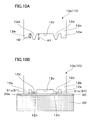
- a leg portion 12e is formed on the end surface 12c of the frame portion 12b on the substrate 20 side in addition to the protruding portion 12d.
- the protrusion 12d is provided in a state sandwiched between the legs 12e, and as shown in FIG. 10A, the height H1 of the protrusion 12d is higher than the height H2 of the legs 12e before joining. .
- the protruding portion 12d has substantially the same height as the leg portion 12e in the melted state. At the time of joining, if the projection 12d is melted using electric heat and the heating is terminated when the leg 12e comes into contact with the substrate 20, the optical element 10 is more stably supported by the leg 12e. Become.
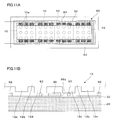
- legs 12e may be provided so as to be sandwiched between each pair of protrusions 12d as shown in FIGS. 11A and 11B.
- the position of the leg part 12e can be changed suitably, for example, you may provide the leg part 12e also between the lens elements 10a.
- the lens element 10a has a light guide 11g on the substrate 20 side instead of the second optical surface 11b in the first embodiment.
- the light guide portion 11g is columnar and has a flat surface 11c at the lower end.
- the light guide portion 11g may be cylindrical or prismatic, and may or may not have a taper.
- a light shielding part 11r is formed on the side surface of the light guide part 11g to prevent intrusion of external light.
- the light shielding part 11r is formed, for example, by attaching a black light shielding film, forming a black light shielding film, or applying a texture.
- the light guide 11g corresponds to each lens element 10a. When the light emitting element 22 emits light in the light source unit 200 including the joined body 100, the light passes through the substrate 20, the light guide 11g, and the lens element 10a. Then, the light is emitted from the first optical surface 11a to form an image.
- a projection 12d is provided on the end surface 12c of the frame portion 12b of the optical element 10.
- the flat surface 11c of the light guide portion 11g comes into contact with the substrate 20 in a state where the projection 12d is melted using electric heat and the optical element 10 and the substrate 20 are joined.
- a plurality of optical elements 10 may be arranged on one substrate 20 as in the second embodiment.
- the joined body according to the seventh embodiment will be described.
- the joined body according to the seventh embodiment is obtained by partially changing the joined body according to the sixth embodiment, and matters that are not particularly described are the same as those in the sixth embodiment.
- the liquid LQ is sealed in a sealed space formed between the optical element 10 that is the first member and the substrate 20 that is the second member.
- a liquid resin a material without an ultraviolet curing or thermosetting initiator
- oil or the like is used.
- the lens element 10a has a light guide portion 11g on the substrate 20 side instead of the second optical surface 11b in the first embodiment.
- 11 g of light guides are columnar, and have the recessed part 11k for filling the liquid LQ in a lower end part.
- a protrusion 11p is provided on the outer peripheral portion 11m of the light guide portion 11g.
- a light shielding part 11r is formed on the side surface of the light guide part 11g to prevent intrusion of external light.
- the liquid LQ is filled in the recess 11k before bonding, and these are bonded in a state where the liquid LQ is sandwiched between the optical element 10 and the substrate 20.
- the substrate 20 is plate-shaped, and if the joint surface between the optical element 10 and the substrate 20 is large, the substrate 20 may be warped. Therefore, it is possible to prevent the optical path from being obstructed by reflection loss by limiting the joint surface to the outer periphery and enclosing, for example, liquid LQ having a refractive index equivalent to that of the optical element 10 inside.
- a plurality of optical elements 10 may be arranged on one substrate 20 as in the second embodiment.
- the joined body etc. which concern on embodiment were demonstrated, the joined body etc. which concern on this invention are not restricted to said thing.
- the shape and size of the optical elements 10 and 50 can be changed as appropriate according to the application and function.
- the first member and the second member are not limited to the optical element 10 and the substrate 20, respectively, and can be appropriately changed according to the application.
- the optical element 10 may be provided with the protrusions 12d and 11p, and the resin around the electric heating portion 90 may be melted and bonded.
- the optical element 10 is not limited to an array-shaped optical element, and may be one as in the first embodiment.
- a plurality of optical elements 10 having lens elements 10a may be arranged, or a plurality of stacked optical elements 10 and 50 as in the third embodiment may be arranged.
- the joined body 100 of the second embodiment may be cut into individual pieces.
Abstract
A bonded body is provided with: an optical element 10 that is a first member formed from a thermoplastic resin; and a substrate 20 that is a second member formed from an inorganic material. The bonded body comprises a molecular adhesive layer 30 between the optical element 10 and the substrate 20. The optical element 10 is chemically bonded to the substrate 20 via the molecular adhesive layer 30 by melting locally with heat from a wiring-type electric heating unit 90 arranged at the boundary or in the vicinity of the boundary between the optical element 10 and the substrate 20.
Description
本発明は、熱可塑性樹脂と無機物とで構成される接合体及び当該接合体の製造方法に関する。
The present invention relates to a joined body composed of a thermoplastic resin and an inorganic material and a method for producing the joined body.
有機物と他の部材とを接合する方法として、シランカップリング剤含有の樹脂や、シランカップリング剤含有のプライマーを使用し、有機基材と無機基材とを接合する方法がある(例えば、特許文献1、2参照)。また、有機物と他の部材とを接合するさらに別の方法として、レーザー光を用いた異材接合方法によって、狙った位置のみを接合するという方法がある(例えば、特許文献3参照)。
As a method of joining an organic substance and another member, there is a method of joining an organic substrate and an inorganic substrate using a resin containing a silane coupling agent or a primer containing a silane coupling agent (for example, a patent) References 1 and 2). Further, as another method for joining an organic substance and another member, there is a method in which only a target position is joined by a different material joining method using laser light (see, for example, Patent Document 3).
しかしながら、特許文献1、2の接合方法では、基材以外の組成物が接合界面に存在するため、基材の耐環境性以外に接合材(具体的には、樹脂やプライマー)の耐環境性も考慮しなければならない。例えば吸湿性の面でいえば、接合材の吸湿性が無機基材よりも高ければ膨潤し、接合部が剥がれるおそれがある。また、接合部の吸湿性が低ければ有機基材の膨潤負荷に耐えきれず、接合材が破壊されるおそれがある。また、量産において接合が良好な状態を再現させるために、シランカップリング剤と接合材とを混ぜ合わせる際の各含有量を管理しなければなない。さらに、特許文献1、2のように面で圧着するような方法は、シートやフィルムの接合には向いているが、熱を一様に伝えることができないため、形状のある部品を部分的に接合することが困難である。
However, in the joining methods of Patent Documents 1 and 2, since a composition other than the base material is present at the joint interface, in addition to the environmental resistance of the base material, the environmental resistance of the joining material (specifically, resin or primer). Must also be considered. For example, in terms of hygroscopicity, if the hygroscopic property of the bonding material is higher than that of the inorganic base material, the bonding material may swell and peel off. In addition, if the hygroscopicity of the bonded portion is low, the bonded material cannot be fully endured and the bonded material may be destroyed. In addition, in order to reproduce a good bonding state in mass production, it is necessary to manage each content when the silane coupling agent and the bonding material are mixed. Furthermore, methods such as Patent Documents 1 and 2 that are pressure-bonded on the surface are suitable for joining sheets and films. It is difficult to join.
また、特許文献3の接合方法では、レーザー光を吸収する材料と、レーザー光を透過する材料との接合に限定され、例えば透明な部材同士や、黒色の部材同士の接合が困難である。
Further, the bonding method of Patent Document 3 is limited to bonding of a material that absorbs laser light and a material that transmits laser light, and for example, it is difficult to bond transparent members or black members.
本発明は、熱可塑性樹脂及び無機物という互いに異なる部材が部分的に接合され、かつ接合状態が良好な接合体を提供することを目的とする。
An object of the present invention is to provide a bonded body in which different members such as a thermoplastic resin and an inorganic material are partially bonded and in a good bonded state.
また、本発明は、この種の接合体の製造方法を提供することを目的とする。
The present invention also aims to provide a method for producing this type of joined body.
上記課題を解決するため、本発明に係る接合体は、熱可塑性樹脂で形成される第1部材と、無機物で形成される第2部材とを備え、第1部材と第2部材との間に分子接着剤層を有し、第1部材は、第1及び第2部材間の境界又は境界近傍に配置された配線状の電熱部からの熱で局所的に溶融されることにより分子接着剤層を介して第2部材に化学的に接合されている。ここで、分子接着剤層とは、第1及び第2部材のいずれとも共有結合をする接着剤単体で構成されるものであり、基本的に他の接着部材を含まない。
In order to solve the above-described problem, a joined body according to the present invention includes a first member formed of a thermoplastic resin and a second member formed of an inorganic material, and the first member is interposed between the first member and the second member. The molecular adhesive layer has a molecular adhesive layer, and the first member is locally melted by heat from a wiring-shaped electrothermal portion disposed at or near the boundary between the first and second members. It is chemically joined to the 2nd member via. Here, the molecular adhesive layer is composed of a single adhesive that is covalently bonded to both the first and second members, and basically does not include other adhesive members.
上記接合体によれば、分子接着剤層を用いた化学結合(具体的には、共有結合)によって、熱可塑性樹脂及び無機物という互いに異なる部材を接合することができる。分子接着剤は、例えばシランカップリング剤のみで実質的に構成される場合のように、他の接合部材を基本的に混合しないため、安定した結合力を得ることができる。また、分子接着剤層は、共有結合をするため、共有結合しない接着剤層と比較して硬化時に収縮等が発生せず、第1及び第2部材間の位置ずれを防ぐことができる。また、分子接着剤層を介した接合は、共有結合しない接着剤層のように硬化反応が完了するまで固定する必要がなく、接合温度や冷却方法等の条件を適宜設定することで比較的短時間で行うことができる。また、電熱を利用して第1及び第2部材を接合するため、目標箇所を局所的に(又は選択的に)接合させることができる。接合時に溶融する熱可塑性樹脂は微少量であるため、この溶融した樹脂の収縮量は、全体が液体状の接着剤が硬化する場合の収縮量よりもはるかに小さく、硬化収縮や溶融時の熱影響が非常に小さい。そのため、第1及び第2部材間の位置ずれに影響しにくい。
According to the above joined body, different members such as a thermoplastic resin and an inorganic material can be joined by chemical bonding (specifically, covalent bonding) using a molecular adhesive layer. Since the molecular adhesive is basically not mixed with other bonding members, for example, as in the case where the molecular adhesive is substantially composed of only the silane coupling agent, a stable bonding force can be obtained. In addition, since the molecular adhesive layer is covalently bonded, shrinkage or the like does not occur at the time of curing as compared with an adhesive layer that is not covalently bonded, and positional displacement between the first and second members can be prevented. In addition, the bonding through the molecular adhesive layer does not need to be fixed until the curing reaction is completed unlike the adhesive layer that is not covalently bonded, and is relatively short by appropriately setting conditions such as the bonding temperature and the cooling method. Can be done in time. Moreover, since the first and second members are joined using electric heat, the target location can be joined locally (or selectively). Since the amount of thermoplastic resin that melts during bonding is very small, the amount of shrinkage of the melted resin is much smaller than the amount of shrinkage that occurs when the liquid adhesive is cured as a whole. The impact is very small. Therefore, it is difficult to affect the positional deviation between the first and second members.
本発明に係る接合体の製造方法は、熱可塑性樹脂で形成される第1部材及び無機物で形成される第2部材間の境界又は境界近傍に配線状の電熱部を設け、第2部材の第1部材に対向する面に分子接着剤層を設け、第1部材を電熱部からの熱で局所的に溶融して分子接着剤層を介して第2部材に化学的に接合させる。
In the method for manufacturing a joined body according to the present invention, a wiring-shaped electrothermal portion is provided at or near the boundary between the first member formed of a thermoplastic resin and the second member formed of an inorganic substance, and the second member A molecular adhesive layer is provided on the surface facing one member, and the first member is locally melted by heat from the electric heating portion and chemically bonded to the second member through the molecular adhesive layer.
上記接合体の製造方法によれば、分子接着剤層を用いた化学結合(共有結合)によって熱可塑性樹脂及び無機物という互いに異なる部材を安定して接合することができる。また、分子接着剤層は、硬化時に収縮等が発生せず、第1及び第2部材間の位置ずれを防ぐことができる。また、分子接着剤層を介した接合は、比較的短時間で行うことができる。また、電熱を利用して第1及び第2部材を接合するため、局所的に接合させることができる。接合時に溶融する熱可塑性樹脂は微少量であるため、硬化収縮や溶融時の熱影響が非常に小さく、第1及び第2部材間の位置ずれに影響しにくい。
According to the above method for producing a joined body, different members such as a thermoplastic resin and an inorganic substance can be stably joined by chemical bonding (covalent bonding) using a molecular adhesive layer. Further, the molecular adhesive layer does not shrink during curing, and can prevent displacement between the first and second members. Further, the bonding via the molecular adhesive layer can be performed in a relatively short time. Moreover, since the first and second members are joined using electric heat, they can be joined locally. Since the thermoplastic resin that melts at the time of joining is a very small amount, the thermal influence during curing shrinkage and melting is very small, and the positional deviation between the first and second members is hardly affected.
〔第1実施形態〕
以下、図面を参照しつつ、本発明の第1実施形態に係る接合体等について説明する。図1A及び1Bに示すように、接合体100は、第1部材である光学素子10と第2部材である基板20とを有する。光学素子10と基板20とは、XY面に垂直なZ軸方向に積み重ねられて接合されている。接合体100は、例えば基板20に発光素子22を設けることにより、光源ユニット200として利用することができる。 [First Embodiment]
Hereinafter, the joined body etc. which concern on 1st Embodiment of this invention are demonstrated, referring drawings. As shown in FIGS. 1A and 1B, the joinedbody 100 includes an optical element 10 that is a first member and a substrate 20 that is a second member. The optical element 10 and the substrate 20 are stacked and joined in the Z-axis direction perpendicular to the XY plane. The joined body 100 can be used as the light source unit 200 by providing the light emitting element 22 on the substrate 20, for example.
以下、図面を参照しつつ、本発明の第1実施形態に係る接合体等について説明する。図1A及び1Bに示すように、接合体100は、第1部材である光学素子10と第2部材である基板20とを有する。光学素子10と基板20とは、XY面に垂直なZ軸方向に積み重ねられて接合されている。接合体100は、例えば基板20に発光素子22を設けることにより、光源ユニット200として利用することができる。 [First Embodiment]
Hereinafter, the joined body etc. which concern on 1st Embodiment of this invention are demonstrated, referring drawings. As shown in FIGS. 1A and 1B, the joined
光学素子(第1部材)10は、利用しようとする波長範囲の光を透過し得る光透過性を有する部材であり、例えば可視光領域の波長の光を透過する場合は透明の部材である。光学素子10は、有機物である熱可塑性樹脂で形成されている。熱可塑性樹脂としては、電気による熱、すなわち電熱で溶融するものであり、例えばCOP(シクロオレフィンポリマー)、PMMA(アクリル)、PC(ポリカーボネート)等が用いられる。光学素子10は、光軸OA方向から見て略円形の輪郭を有する。光学素子10は、レンズ要素10aと、レンズ要素10aを周囲から支持する支持部10bとを有する。レンズ要素10aは、例えば両凸の非球面レンズであり、第1光学面11aと第2光学面11bとを有する。支持部10bは、平板状の平板部分12aと、平板部分12aの外周から光軸OAに平行に延びる環状の枠部分12bとを有する。枠部分12bの基板20側の端面12cには、突起部12dが形成されている。突起部12dは、光学素子10と基板20とを接合したい部分に形成されている。図示の例では、突起部12dは、2重の円環状となっている。突起部12dの配置は、後述する電熱部90の配線形状に対応したものとなっている。接合前の突起部12dは、電熱部90と接触させた際に安定するように先端が平坦面であることが好ましい。突起部12dの断面形状は、図3Aに示すような台形に限らず、例えば半球形や楕円形を切り欠いた形状であってもよい。光学素子10は、例えば集光レンズとして用いられる。
The optical element (first member) 10 is a member having optical transparency that can transmit light in a wavelength range to be used. For example, the optical element (first member) 10 is a transparent member when transmitting light having a wavelength in the visible light region. The optical element 10 is formed of a thermoplastic resin that is an organic substance. The thermoplastic resin is one that melts by electricity, that is, electric heat. For example, COP (cycloolefin polymer), PMMA (acrylic), PC (polycarbonate), and the like are used. The optical element 10 has a substantially circular outline when viewed from the optical axis OA direction. The optical element 10 includes a lens element 10a and a support portion 10b that supports the lens element 10a from the periphery. The lens element 10a is a biconvex aspheric lens, for example, and has a first optical surface 11a and a second optical surface 11b. The support portion 10b has a flat plate portion 12a and an annular frame portion 12b extending in parallel with the optical axis OA from the outer periphery of the flat plate portion 12a. A protrusion 12d is formed on the end surface 12c of the frame portion 12b on the substrate 20 side. The protrusion 12d is formed at a portion where the optical element 10 and the substrate 20 are to be joined. In the example shown in the figure, the protrusion 12d has a double annular shape. The arrangement of the protrusion 12d corresponds to the wiring shape of the electric heating unit 90 described later. It is preferable that the protrusion 12d before joining has a flat surface at the tip so as to be stable when brought into contact with the electric heating part 90. The cross-sectional shape of the protrusion 12d is not limited to the trapezoid as shown in FIG. 3A, and may be a shape obtained by cutting out a hemisphere or an ellipse, for example. The optical element 10 is used as a condensing lens, for example.
基板(第2部材)20は、透明で光透過性を有する板状部材であり、無機物であるガラスで形成されたガラス基板である。基板20の第1面20aには、光学素子10が接合されている。また、既に説明したように、図示の例では、基板20の第2面20bには、発光素子22が設けられている。発光素子22の中心は、光学素子10の光軸OA上に配置される。発光素子22としては、例えば有機ELやLED素子等が用いられる。
The substrate (second member) 20 is a transparent and light-transmitting plate-like member, and is a glass substrate formed of glass that is an inorganic substance. The optical element 10 is bonded to the first surface 20 a of the substrate 20. As already described, in the illustrated example, the light emitting element 22 is provided on the second surface 20 b of the substrate 20. The center of the light emitting element 22 is disposed on the optical axis OA of the optical element 10. As the light emitting element 22, for example, an organic EL or LED element is used.
基板20には、光学素子10を接合する前に予め、光学素子10に対向する面である第1面20aに分子を活性化させる表面処理が施されている。表面処理は、第1面20aに対して一部又は全体に施される。表面処理として、例えばコロナ処理、プラズマ処理、オゾン処理、及び紫外線(UV)処理等が行われる。これにより、光学素子10及び基板20間の結合力をより強くすることができる。なお、光学素子10の枠部分12bの端面12c(特に突起部12dの先端)にも分子を活性化させる表面処理が施されていてもよい。基板20及び光学素子10の両方に上記表面処理を施すことにより、より結合力を強くすることができる。なお、基板20及び光学素子10に上記表面処理を施さなくてもよく、イソプロピルアルコール(IPA)等で表面を拭き取り清掃するだけでもよい。
Before the optical element 10 is bonded to the substrate 20, a surface treatment for activating molecules is performed on the first surface 20 a that is a surface facing the optical element 10 in advance. The surface treatment is performed on a part or the whole of the first surface 20a. As the surface treatment, for example, corona treatment, plasma treatment, ozone treatment, and ultraviolet (UV) treatment are performed. Thereby, the coupling force between the optical element 10 and the substrate 20 can be further increased. Note that the end surface 12c of the frame portion 12b of the optical element 10 (particularly, the tip of the protrusion 12d) may be subjected to a surface treatment that activates molecules. By applying the surface treatment to both the substrate 20 and the optical element 10, the bonding strength can be further increased. Note that the substrate 20 and the optical element 10 may not be subjected to the above surface treatment, and may be simply wiped and cleaned with isopropyl alcohol (IPA) or the like.
光学素子10と基板20との間、具体的には基板20の第1面20aには、分子接着剤層30が設けられている。分子接着剤層30は、光学素子10の枠部分12bに対応する位置に設けられてもよいし、基板20の第1面20aの全面に設けられてもよい。ここで、分子接着剤層30とは、光学素子10及び基板20のいずれとも共有結合をする接着剤単体で構成されるものであり、基本的に他の接着部材を含まない。図1A等では、説明の都合上、分子接着剤層30に厚みがあるように図示しているが、実際には、分子接着剤層30は分子サイズであり、接着剤の硬化収縮を考慮する必要がない。図2Bに示すように、基板20と分子接着剤層30とは、分子接着剤の加水分解性基が加水分解反応及び縮合反応を経て共有結合G1で結合し、光学素子10と分子接着剤層30とは、分子接着剤の有機官能基が所定の反応を経て共有結合G2で結合している。接合体100は、光学素子10及び基板20のいずれとも共有結合(化学結合)しているため、耐環境性がよい。分子接着剤層30を形成する分子接着剤としては、例えばシラノール含有接着剤等、具体的にはシランカップリング剤等が用いられる。
A molecular adhesive layer 30 is provided between the optical element 10 and the substrate 20, specifically, on the first surface 20 a of the substrate 20. The molecular adhesive layer 30 may be provided at a position corresponding to the frame portion 12 b of the optical element 10, or may be provided on the entire first surface 20 a of the substrate 20. Here, the molecular adhesive layer 30 is composed of a single adhesive that is covalently bonded to both the optical element 10 and the substrate 20, and basically does not include other adhesive members. In FIG. 1A and the like, for convenience of explanation, the molecular adhesive layer 30 is illustrated as having a thickness, but in reality, the molecular adhesive layer 30 has a molecular size, and the curing shrinkage of the adhesive is taken into consideration. There is no need. As shown in FIG. 2B, the substrate 20 and the molecular adhesive layer 30 are formed by bonding a hydrolyzable group of the molecular adhesive through a covalent bond G1 through a hydrolysis reaction and a condensation reaction, and the optical element 10 and the molecular adhesive layer. 30, an organic functional group of the molecular adhesive is bonded by a covalent bond G2 through a predetermined reaction. Since the bonded body 100 is covalently bonded (chemically bonded) to both the optical element 10 and the substrate 20, the environment resistance is good. As the molecular adhesive that forms the molecular adhesive layer 30, for example, a silanol-containing adhesive or the like, specifically, a silane coupling agent or the like is used.
また、基板20第1面20aと光学素子10の枠部分12bとの間の境界又は境界近傍には、電熱部90が配置されている。電熱部90は、光学素子10と基板20とを接合したい部分に設けられている。電熱部90は、配線状の電熱線91で形成されている。電熱線91としては、例えば安価なニクロム線等が用いられ、第1部材である光学素子10を加熱及び溶融させて安価に接合することができる。図示の例では、電熱部90は、2重の円環状(内側の電熱線91a及び外側の電熱線91bを含むもの)となっている。なお、電熱部90の配置は、円環状に限らず、配線を妨げない配置であれば、例えば光軸OAに垂直な方向の線状等でもよい。光学素子10と基板20とは分子接着剤層30を介して化学的に接合されている。図2Aに拡大して示すように、光学素子10の突起部12dが電熱部90と接触する部分及びその周辺は、電熱部90からの熱によって溶融しており、この溶融した部分である溶融痕12hが、光学素子10と基板20とを局所的に接合した部分となっている。
Further, an electric heating section 90 is disposed at or near the boundary between the first surface 20a of the substrate 20 and the frame portion 12b of the optical element 10. The electrothermal unit 90 is provided at a portion where the optical element 10 and the substrate 20 are to be joined. The electric heating part 90 is formed of a wiring-like electric heating wire 91. As the heating wire 91, for example, an inexpensive nichrome wire or the like is used, and the optical element 10 as the first member can be heated and melted to be bonded at a low cost. In the example shown in the drawing, the heating section 90 has a double annular shape (including an inner heating wire 91a and an outer heating wire 91b). Note that the arrangement of the electric heating unit 90 is not limited to an annular shape, and may be, for example, a linear shape in a direction perpendicular to the optical axis OA as long as the arrangement does not hinder wiring. The optical element 10 and the substrate 20 are chemically bonded via a molecular adhesive layer 30. As shown in an enlarged view in FIG. 2A, the portion where the protrusion 12d of the optical element 10 is in contact with the electric heating portion 90 and the periphery thereof are melted by the heat from the electric heating portion 90, and the melting mark is the molten portion. 12 h is a portion where the optical element 10 and the substrate 20 are locally joined.
既に説明したように、接合体100において、光学素子10は、電熱を利用して局所的に溶融することにより分子接着剤層30を介して突起部12dの箇所で基板20に接合されている。つまり、光学素子10及び基板20は、接合されるべき部分のみ接合されている。電熱部からの熱によって光学素子10と基板20との接合界面に熱が発生し、樹脂を溶融させることで、分子接着剤層30が化学反応し、光学素子10及び基板20に対して化学的に結合する。
As already described, in the bonded body 100, the optical element 10 is bonded to the substrate 20 at the position of the protrusion 12d via the molecular adhesive layer 30 by locally melting using electric heat. That is, the optical element 10 and the substrate 20 are bonded only to the portions to be bonded. Heat is generated at the bonding interface between the optical element 10 and the substrate 20 due to the heat from the electric heating portion, and the resin is melted, whereby the molecular adhesive layer 30 chemically reacts and chemically reacts with the optical element 10 and the substrate 20. To join.
以下、接合体の製造方法について説明する。まず、第1部材である光学素子10を成形する。成形方法として、射出成形、モールド成形等が用いられる。図3Aに示すように、光学素子10の枠部分12bの端面12cには、突起部12dが形成されている。光学素子10に電熱部90を設ける場合、例えば樹脂を溶融させて電熱部90の電熱線91を取り付ける。具体的には、図3Aに示すように、転写基板99aに電熱部90の電熱線91を接着剤99bで仮止めした状態で、光学素子10を位置決めしつつ電熱部90上に光学素子10を乗せ、電熱部90からの熱により突起部12dを溶融させ、突起部12dの先端に電熱部90を埋め込む。光学素子10から転写基板99aを取り除くことで、図3Bに示すように、電熱部90が配置された光学素子10が得られる。なお、電熱部90は、基板20に配置してもよく、例えば、電熱線91を引っ張った状態で接着剤99bを用いて基板20上に固定したり、電熱線91に通電して基板20を一部溶融して基板20上に固定したり、基板20の製造時に一体的に固定してもよい。基板20に電熱部90を設ける場合、下記の表面処理や分子接着剤層30の形成前に設けてもよいし、形成後に設けてもよい。
Hereinafter, a method for manufacturing the joined body will be described. First, the optical element 10 as the first member is molded. As the molding method, injection molding, molding, or the like is used. As shown in FIG. 3A, a protrusion 12d is formed on the end surface 12c of the frame portion 12b of the optical element 10. When providing the heating part 90 in the optical element 10, for example, the resin is melted and the heating wire 91 of the heating part 90 is attached. Specifically, as shown in FIG. 3A, the optical element 10 is placed on the electrothermal portion 90 while positioning the optical element 10 in a state where the heating wire 91 of the electrothermal portion 90 is temporarily fixed to the transfer substrate 99a with the adhesive 99b. The protruding portion 12d is melted by the heat from the electric heating portion 90, and the electric heating portion 90 is embedded at the tip of the protruding portion 12d. By removing the transfer substrate 99a from the optical element 10, as shown in FIG. 3B, the optical element 10 in which the electrothermal unit 90 is arranged is obtained. The heating unit 90 may be disposed on the substrate 20. For example, the heating unit 90 may be fixed on the substrate 20 using the adhesive 99 b while the heating wire 91 is pulled, or the heating wire 91 may be energized to attach the substrate 20. It may be partially melted and fixed on the substrate 20 or may be fixed integrally when the substrate 20 is manufactured. When providing the electrothermal part 90 in the board | substrate 20, you may provide before formation of the following surface treatment and the molecular adhesive layer 30, and you may provide after formation.
次に、第2部材である基板20を準備する。基板20の第1面20aに分子を活性化させる表面処理を施す。具体的には、コロナ処理、プラズマ処理、オゾン処理、及び紫外線(UV)処理等を行う。その後、第1面20aに分子接着剤を塗布し、分子接着剤層30を形成する。具体的には、シランカップリング剤を水や有機溶剤等に溶かし、ディッピング、スプレー、スピンコート等の方法で基板20の第1面20aの所定の部分に塗布し、乾燥させる。接合体100を光源ユニット200の用途で用いる場合には、基板20の第2面20bに発光素子22を取り付ける(図1A参照)。この場合、上記処理を行う前に発光素子22を基板20に取り付けておくことが好ましい。分子を活性化させる表面処理は、上述のように分子接着剤層30の形成前に第1面20aに対して行ってもよいし、形成後に行ってもよい。分子接着剤層30の形成後に表面処理を行う場合、分子接着剤層30の表面に表面処理を行うことができ、或いは突起部12dの先端面等に表面処理を行うこともできる。
Next, a substrate 20 as a second member is prepared. A surface treatment for activating molecules is performed on the first surface 20 a of the substrate 20. Specifically, corona treatment, plasma treatment, ozone treatment, ultraviolet (UV) treatment, or the like is performed. Thereafter, a molecular adhesive is applied to the first surface 20 a to form the molecular adhesive layer 30. Specifically, a silane coupling agent is dissolved in water, an organic solvent, or the like, applied to a predetermined portion of the first surface 20a of the substrate 20 by a method such as dipping, spraying, or spin coating, and dried. When the joined body 100 is used for the light source unit 200, the light emitting element 22 is attached to the second surface 20b of the substrate 20 (see FIG. 1A). In this case, it is preferable to attach the light emitting element 22 to the substrate 20 before performing the above processing. The surface treatment for activating molecules may be performed on the first surface 20a before the formation of the molecular adhesive layer 30 as described above, or may be performed after the formation. When the surface treatment is performed after the formation of the molecular adhesive layer 30, the surface treatment can be performed on the surface of the molecular adhesive layer 30, or the surface treatment can be performed on the tip surface of the protrusion 12 d or the like.
次に、図3C等に示すように、光学素子10と基板20とを電熱によって接合させる。接合には、電力供給装置60を用いる(図4参照)。基板20は、支持台61上に固定されている。基板20に光学素子10を積み重ねる際に、基板20と光学素子10とをアライメントする。光学素子10は、基板20の第1面20a上に位置決めした状態で側面から固定してもよい。その後、図4に示すように押圧装置62を光学素子10の端面10sに対して光軸OA方向から押さえ付ける。光軸OA方向から押さえる力は、例えば、1N~10Nとなっている。また、電力供給装置60の電圧は、例えば、0.5V~8V、電流は、例えば、0.1A~2A、接合時間は、例えば、0.1秒~3秒である。光学素子10を基板20に積み重ねた状態で、光学素子10の突起部12dは、最初に基板20に接触している。図3C及び図4に示すように、電力供給装置60を動作させることにより、光学素子10と基板20との接合界面(具体的には、突起部12dの先端及びその周辺)に熱が発生し、図3Dに示すように、光学素子10の突起部12dの先端の樹脂が溶融する。この際、光学素子10の熱可塑性樹脂、基板20のガラス、及び分子接着剤層30であるシランカップリング剤が化学反応し、これらが化学的に結合する。樹脂の溶融は、基板20と接触する部分で発生するため、突起部12dの部分だけ局所的に接合されることになる。光学素子10と基板20との接触部分は、局所的であるため、突起部12dにおいて溶融する樹脂は微少量であり、硬化収縮や溶融時の熱影響が非常に小さくなる。電熱を終了し冷却させることで、光学素子10と基板20とが接合した接合体100又は光源ユニット200が完成する。なお、表面処理、分子接着剤層30の形成、及び電熱による接合の一連の工程を同一の雰囲気下(例えば、不活性の雰囲気下)で行ってもよいし、表面処理の効果を失わなければ、同一の雰囲気下で行わなくてもよい。接合後、電熱部90の電熱線91を引き抜いて除去してもよいし、電熱線91を残して接合体の剛性を向上させてもよい。
Next, as shown in FIG. 3C and the like, the optical element 10 and the substrate 20 are joined by electric heating. The power supply device 60 is used for joining (see FIG. 4). The substrate 20 is fixed on the support base 61. When the optical element 10 is stacked on the substrate 20, the substrate 20 and the optical element 10 are aligned. The optical element 10 may be fixed from the side surface in a state where the optical element 10 is positioned on the first surface 20 a of the substrate 20. Thereafter, as shown in FIG. 4, the pressing device 62 is pressed against the end surface 10 s of the optical element 10 from the direction of the optical axis OA. The force pressed from the direction of the optical axis OA is, for example, 1N to 10N. The voltage of the power supply device 60 is, for example, 0.5 V to 8 V, the current is, for example, 0.1 A to 2 A, and the junction time is, for example, 0.1 seconds to 3 seconds. With the optical element 10 stacked on the substrate 20, the protrusion 12 d of the optical element 10 is first in contact with the substrate 20. As shown in FIGS. 3C and 4, by operating the power supply device 60, heat is generated at the bonding interface between the optical element 10 and the substrate 20 (specifically, the tip of the protrusion 12 d and its periphery). As shown in FIG. 3D, the resin at the tip of the protrusion 12d of the optical element 10 is melted. At this time, the thermoplastic resin of the optical element 10, the glass of the substrate 20, and the silane coupling agent which is the molecular adhesive layer 30 chemically react, and these are chemically bonded. Since the melting of the resin occurs at the portion in contact with the substrate 20, only the portion of the protruding portion 12d is locally bonded. Since the contact portion between the optical element 10 and the substrate 20 is local, only a small amount of resin is melted at the protrusion 12d, and the thermal influence during shrinkage and melting is very small. By finishing the electric heating and cooling, the joined body 100 or the light source unit 200 in which the optical element 10 and the substrate 20 are joined is completed. Note that a series of steps of surface treatment, formation of the molecular adhesive layer 30 and bonding by electric heating may be performed in the same atmosphere (for example, in an inert atmosphere), and the effect of the surface treatment is not lost. , It does not have to be performed in the same atmosphere. After joining, the heating wire 91 of the heating part 90 may be pulled out and removed, or the heating wire 91 may be left to improve the rigidity of the joined body.
上記説明した接合体によれば、分子接着剤層30を用いた化学結合(具体的には、共有結合)によって、熱可塑性樹脂及び無機物という互いに異なる部材(第1部材である光学素子10、及び第2部材である基板20)を接合することができる。分子接着剤層30は、例えばシランカップリング剤のみで実質的に構成される場合のように、他の接合部材を混合しないため、安定した結合力を得ることができる。また、分子接着剤層30は、共有結合をするため、共有結合しない接着剤層と比較して硬化時に収縮等が発生せず、光学素子10と基板20との間の位置ずれを防ぐことができる。また、分子接着剤層30を介した接合は、共有結合しない接着剤層のように硬化反応が完了するまで固定する必要がなく、接合温度や冷却方法等の条件を適宜設定することで比較的短時間で行うことができる。また、電熱を利用して光学素子10と基板20とを接合するため、目標箇所を局所的に(又は選択的に)接合させることができる。接合時に溶融する熱可塑性樹脂は微少量であるため、この溶融した樹脂の収縮量は、全体が液体状の接着剤が硬化する場合の収縮量よりもはるかに小さく、硬化収縮や溶融時の熱影響が非常に小さい。そのため、光学素子10と基板20との間の位置ずれに影響しにくい。
According to the above-described bonded body, the different members (the optical element 10 as the first member) and the thermoplastic resin and the inorganic substance by chemical bonding (specifically, covalent bonding) using the molecular adhesive layer 30, and The board | substrate 20) which is a 2nd member can be joined. Since the molecular adhesive layer 30 is not mixed with other joining members, for example, as in the case where the molecular adhesive layer 30 is substantially composed of only a silane coupling agent, a stable bonding force can be obtained. Further, since the molecular adhesive layer 30 is covalently bonded, shrinkage or the like does not occur at the time of curing as compared with an adhesive layer that is not covalently bonded, and the positional deviation between the optical element 10 and the substrate 20 can be prevented. it can. In addition, the bonding through the molecular adhesive layer 30 does not need to be fixed until the curing reaction is completed as in the case of an adhesive layer that is not covalently bonded, and can be relatively set by appropriately setting conditions such as a bonding temperature and a cooling method. It can be done in a short time. Further, since the optical element 10 and the substrate 20 are bonded using electric heat, the target location can be bonded locally (or selectively). Since the amount of thermoplastic resin that melts during bonding is very small, the amount of shrinkage of the melted resin is much smaller than the amount of shrinkage that occurs when the liquid adhesive is cured as a whole. The impact is very small. For this reason, it is difficult to affect the positional deviation between the optical element 10 and the substrate 20.
また、第1部材である光学素子10と第2部材である基板20とが透明で光透過性を有する部材であっても、電熱を利用して樹脂を溶融しているため、接合状態が良好となる。つまり、光学素子10及び基板20の色に関係なく接合でき、両者は透明な部材に限らず、例えば黒色の部材を用いてもよい。
Even if the optical element 10 as the first member and the substrate 20 as the second member are transparent and light transmissive members, the bonding state is good because the resin is melted using electric heat. It becomes. That is, the optical element 10 and the substrate 20 can be joined regardless of the color, and both are not limited to transparent members, and for example, a black member may be used.
また、樹脂を溶融させ分子接着剤層30を介して行う接合は、光透過性を有し、歪みを嫌い、耐環境性を有する部材、特に位置ずれに関して重要度が高いものの接合に適合しており、樹脂製の第1部材である光学素子10とガラス製の第2部材である基板20とを組み合わせた接合体100でも良好な接合状態を達成できる。
In addition, the bonding performed by melting the resin and passing through the molecular adhesive layer 30 is suitable for bonding members that have light transmission properties, dislike distortion, and have environmental resistance, particularly those that are highly important with respect to displacement. In addition, even in the joined body 100 in which the optical element 10 that is the first member made of resin and the substrate 20 that is the second member made of glass are combined, a good joined state can be achieved.
〔実施例1〕
以下、本実施形態の実施例1について説明する。本実施例1において、試料として熱可塑性樹脂を用いて第1部材を射出成形によって成形した。簡単のために、第1部材は、光学素子ではなく、四角柱状の部材とした。突起部の断面は、台形であり、その寸法は、高さを1mm、根元側の幅を1.5mm、先端側の幅を0.5mm、長さを5mmとした。突起部は、2列に並んで形成されており、2つの突起部の先端間の間隔は、3mmとした。熱可塑性樹脂には、シクロオレフィンポリマー(COP)(ZEONEX E48R(ZEONEX社製))、ポリカーボネート(PC)(PC1600(タキロン社製))、及びアクリル(PMMA)(デラグラスK(旭化成テクノプラス製))を用いた。第2部材として、ガラス板を用いた。電熱部を形成する電熱線には、直径0.3mmのニクロム線を用いた。第2部材の第1部材との接合界面である第1面には、分子を活性化させる表面処理を施したものと施していないものとを準備した。分子を活性化させる表面処理では、UVオゾン洗浄又はプラズマ洗浄を行った。UVオゾン洗浄は、UV波長(185~253nm)で、照射距離を10mm、洗浄時間を5分という条件で行った。プラズマ洗浄は、圧力を10Pa、出力を150W、洗浄時間を10秒という条件で行った。なお、分子を活性化させる表面処理を施さない第2部材では、第1面をIPAで拭き取り清掃した。上記処理後、第2部材の第1面に分子接着剤を塗布し、分子接着剤層を形成した。分子接着剤には、シラノール含有接着剤(シランカップリング剤SZ-6300(東レ・ダウコーニング社製)又はシランカップリング剤Z-6011(東レ・ダウコーニング社製))を用いた。その後、第1部材と第2部材とを電熱によって接合させ、接合体を作製した。接合は、電圧8V、電流2A、接合時の荷重10N、接合時間を3秒という条件で行った。 [Example 1]
Hereinafter, Example 1 of the present embodiment will be described. In Example 1, the first member was molded by injection molding using a thermoplastic resin as a sample. For simplicity, the first member is not an optical element but a quadrangular prism-shaped member. The cross section of the protrusion was trapezoidal, and the dimensions were 1 mm in height, 1.5 mm in width on the base side, 0.5 mm in width on the tip side, and 5 mm in length. The protrusions are formed in two rows, and the distance between the tips of the two protrusions is 3 mm. Thermoplastic resins include cycloolefin polymer (COP) (ZEONEX E48R (manufactured by ZEONEX)), polycarbonate (PC) (PC1600 (manufactured by Takiron)), and acrylic (PMMA) (Delagrass K (manufactured by Asahi Kasei Technoplus)) Was used. A glass plate was used as the second member. A nichrome wire having a diameter of 0.3 mm was used as the heating wire forming the heating portion. On the first surface, which is a bonding interface between the second member and the first member, a surface treated to activate molecules and a surface not subjected to surface treatment were prepared. In the surface treatment for activating molecules, UV ozone cleaning or plasma cleaning was performed. The UV ozone cleaning was performed under the conditions that the UV wavelength (185 to 253 nm), the irradiation distance was 10 mm, and the cleaning time was 5 minutes. Plasma cleaning was performed under the conditions of a pressure of 10 Pa, an output of 150 W, and a cleaning time of 10 seconds. In addition, the 2nd member which does not perform the surface treatment which activates a molecule | numerator wiped and cleaned the 1st surface with IPA. After the treatment, a molecular adhesive was applied to the first surface of the second member to form a molecular adhesive layer. As the molecular adhesive, a silanol-containing adhesive (silane coupling agent SZ-6300 (manufactured by Toray Dow Corning) or silane coupling agent Z-6011 (manufactured by Toray Dow Corning)) was used. Then, the 1st member and the 2nd member were joined by electric heating, and the joined object was produced. Joining was performed under the conditions of a voltage of 8 V, a current of 2 A, a load of 10 N during joining, and a joining time of 3 seconds.
表1に第1部材と第2部材との接合状態を示す。表1中、分子接着剤として、シランカップリング剤SZ-6300を「A」、シランカップリング剤Z-6011を「B」と表記した。接合体の接合状態の評価は、第1及び第2部材の剥離又は破断時の接合力で判断した。接合力は、第2部材を固定し、第1部材を治具を用いてチャックして垂直に引き上げ、プルゲージを用いて測定した。測定結果は、0N≦F<2Nを不良(符号「×」)、2N≦F<25Nを可(符号「△」)、25N≦F<50Nを良(符号「○」)、50N≦Fを優(符号「◎」)として評価した。ただし、Fは接合力である。
〔表1〕
 表1に示すように、電熱によって分子接着剤層を介して第1及び第2部材を接合することで、接合体は2N≦Fの接合力を有することがわかる。また、分子を活性化させる表面処理を施すことで、第1及び第2部材の接合体の接合力がより強くなることがわかる。なお、比較のため、アクリル系光硬化性接着剤を用いて、第1部材と第2部材とを接着したところ、表面処理の有無に関わらず、接合体の強度は不良「×」となった。
Table 1 shows the joined state of the first member and the second member. In Table 1, as molecular adhesives, silane coupling agent SZ-6300 is indicated as “A”, and silane coupling agent Z-6011 is indicated as “B”. The evaluation of the joined state of the joined body was judged by the joining force at the time of peeling or breaking of the first and second members. The bonding force was measured using a pull gauge, with the second member fixed, the first member chucked using a jig, pulled up vertically. As a result of the measurement, 0N ≦ F <2N is defective (symbol “×”), 2N ≦ F <25N is acceptable (symbol “Δ”), 25N ≦ F <50N is satisfactory (symbol “◯”), and 50N ≦ F is satisfied. It was evaluated as excellent (symbol “◎”). However, F is a joining force.
表1に示すように、電熱によって分子接着剤層を介して第1及び第2部材を接合することで、接合体は2N≦Fの接合力を有することがわかる。また、分子を活性化させる表面処理を施すことで、第1及び第2部材の接合体の接合力がより強くなることがわかる。なお、比較のため、アクリル系光硬化性接着剤を用いて、第1部材と第2部材とを接着したところ、表面処理の有無に関わらず、接合体の強度は不良「×」となった。
Table 1 shows the joined state of the first member and the second member. In Table 1, as molecular adhesives, silane coupling agent SZ-6300 is indicated as “A”, and silane coupling agent Z-6011 is indicated as “B”. The evaluation of the joined state of the joined body was judged by the joining force at the time of peeling or breaking of the first and second members. The bonding force was measured using a pull gauge, with the second member fixed, the first member chucked using a jig, pulled up vertically. As a result of the measurement, 0N ≦ F <2N is defective (symbol “×”), 2N ≦ F <25N is acceptable (symbol “Δ”), 25N ≦ F <50N is satisfactory (symbol “◯”), and 50N ≦ F is satisfied. It was evaluated as excellent (symbol “◎”). However, F is a joining force.
[Table 1]
As shown in Table 1, it can be seen that the joined body has a joining force of 2N ≦ F by joining the first and second members via the molecular adhesive layer by electric heating. Moreover, it turns out that the joining force of the joined body of the 1st and 2nd member becomes stronger by performing the surface treatment which activates a molecule | numerator. For comparison, when the first member and the second member were bonded using an acrylic photo-curable adhesive, the strength of the joined body was defective “x” regardless of the presence or absence of the surface treatment. .
〔表1〕
[Table 1]
〔第2実施形態〕
以下、第2実施形態に係る接合体について説明する。なお、第2実施形態に係る接合体は、第1実施形態の接合体を一部変更したものであり、特に説明しない事項は、第1実施形態と同様である。 [Second Embodiment]
Hereinafter, the joined body according to the second embodiment will be described. Note that the joined body according to the second embodiment is obtained by partially changing the joined body according to the first embodiment, and matters that are not particularly described are the same as those in the first embodiment.
図5A及び5Bに示すように、本実施形態では、1つの第2部材である基板20に複数の第1部材である光学素子10が分子接着剤層30を介して局所的に接合されている。また、基板20と光学素子10との間には、遮光体40が設けられている。接合体100を含む光源ユニット200は、例えばプリントヘッド等に用いられる。
As shown in FIGS. 5A and 5B, in this embodiment, a plurality of optical elements 10 as first members are locally bonded to a substrate 20 as a second member via a molecular adhesive layer 30. . A light shield 40 is provided between the substrate 20 and the optical element 10. The light source unit 200 including the joined body 100 is used for a print head or the like, for example.
1つの光学素子10は、光軸OA方向から見て四角形の輪郭を有する。光学素子10は、複数のレンズ要素10aと、複数のレンズ要素10aを周囲から支持する支持部10bとを有する。レンズ要素10aは、アレイ状に設けられている。支持部10bは、平板状の平板部分12aの対向する2つの辺から平板部分12aに垂直な方向に延びる枠部分12bを有する。枠部分12bの端面12cには、突起部12dが形成されている。
One optical element 10 has a rectangular outline when viewed from the direction of the optical axis OA. The optical element 10 includes a plurality of lens elements 10a and a support portion 10b that supports the plurality of lens elements 10a from the periphery. The lens elements 10a are provided in an array. The support portion 10b includes a frame portion 12b extending in a direction perpendicular to the flat plate portion 12a from two opposing sides of the flat plate portion 12a. A protrusion 12d is formed on the end surface 12c of the frame portion 12b.
本実施形態において、図6A及び6Bに示すように、電熱部90は、電熱シート92に形成されている電熱配線93である。電熱シート92は、光学素子10と基板20との間に設けられた枠状の薄膜である。つまり、電熱シート92は、光学素子10の枠部分12b(図5B参照)に対応する位置に設けられており、レンズ要素10aに対応する位置には設けられていない。電熱シート92には、微細な孔92aが部分的に形成されており、光学素子10の樹脂が溶融したときに、溶融した樹脂が電熱シート92の孔92aを通過して、分子接着剤層30を介して基板20と接合できるようになっている。なお、電熱シート92全体がメッシュ状であってもよい。電熱配線93は、光学素子10の突起部12dの位置に対応するように形成されている。電熱配線93は、電熱シート92に電熱線を埋め込んで形成してもよいし、例えば電熱シート92がメッシュ状の場合、金属の配線パターンを印刷することで形成してもよい。
In this embodiment, as shown in FIGS. 6A and 6B, the electrothermal unit 90 is an electrothermal wiring 93 formed on an electrothermal sheet 92. The electrothermal sheet 92 is a frame-shaped thin film provided between the optical element 10 and the substrate 20. That is, the electrothermal sheet 92 is provided at a position corresponding to the frame portion 12b (see FIG. 5B) of the optical element 10, and is not provided at a position corresponding to the lens element 10a. Fine holes 92a are partially formed in the electric heating sheet 92. When the resin of the optical element 10 is melted, the molten resin passes through the holes 92a of the electric heating sheet 92, and the molecular adhesive layer 30. It can be joined to the substrate 20 via The entire electrothermal sheet 92 may be mesh. The electric heating wiring 93 is formed so as to correspond to the position of the protrusion 12 d of the optical element 10. The electric heating wire 93 may be formed by embedding an electric heating wire in the electric heating sheet 92. For example, when the electric heating sheet 92 has a mesh shape, it may be formed by printing a metal wiring pattern.
図5Bに示すように、基板20の第2面20bには、複数の発光素子22が光学素子10のレンズ要素10aに対応する位置にアレイ状に設けられている。
As shown in FIG. 5B, a plurality of light emitting elements 22 are provided in an array on the second surface 20 b of the substrate 20 at positions corresponding to the lens elements 10 a of the optical element 10.
遮光体40は、平板状の部材であり、発光素子22の不要光を遮光する。遮光体40としては、例えば黒色等の光吸収性の粒子を含むガラス製又は樹脂製の基板、黒色に塗装された金属製の基板等を用いる。遮光体40には、光学素子10のレンズ要素10aに対応する位置に開口40aが形成されている。遮光体40は、基板20側に接合されている。遮光体40は、分子接着剤以外の接着剤で接着されてもよいが、材料の組み合わせによって、光学素子10と基板20との接合と同様に、電熱を利用して接合させてもよい。例えば、遮光体40の材料が、基板20の材料である無機物とは異なる樹脂であれば、分子接着剤層130を介して接合することができる。
The light shield 40 is a flat plate member that shields unnecessary light from the light emitting element 22. As the light shielding body 40, for example, a glass or resin substrate containing light-absorbing particles such as black, a metal substrate painted black, or the like is used. An opening 40 a is formed in the light shielding body 40 at a position corresponding to the lens element 10 a of the optical element 10. The light shield 40 is bonded to the substrate 20 side. The light blocking body 40 may be bonded with an adhesive other than a molecular adhesive, but may be bonded using electric heat in the same manner as the bonding between the optical element 10 and the substrate 20 depending on the combination of materials. For example, if the material of the light shielding body 40 is a resin different from the inorganic material that is the material of the substrate 20, the light shielding body 40 can be bonded via the molecular adhesive layer 130.
接合体100の製造において、基板20の第1面20a上に複数の光学素子10を全て並べた状態で電熱で一度に接合させてもよいし、1個又は数個単位で光学素子10を並べて複数回に分けて電熱で接合させてもよい。
In the manufacture of the bonded body 100, the plurality of optical elements 10 may be bonded together by electric heating in a state where all the optical elements 10 are arranged on the first surface 20 a of the substrate 20, or the optical elements 10 are arranged in units of one or several. You may make it join in several times by electroheating.
本実施形態の接合体において、電熱による接合は高ワット数であれば比較的短時間で行うことができるため、複数の光学素子(第1部材)10を一度に、又は複数回に分けて接合させても比較的短時間で接合でき、生産性が良い。
In the joined body of the present embodiment, joining by electric heating can be performed in a relatively short time as long as the wattage is high, so that a plurality of optical elements (first members) 10 are joined at once or divided into a plurality of times. Even if it makes it, it can join in a comparatively short time and productivity is good.
また、電熱配線93が電熱シート92に形成されているため、電熱部90の形状が安定し、組み付けも容易である。これにより、光学素子10の溶融すべき部分を精度良く溶融することができる。また、光学素子10又は基板20上に電熱線を直接パターンニングする工程が不要であるため、生産効率が良い。
Moreover, since the electric heating wiring 93 is formed on the electric heating sheet 92, the shape of the electric heating portion 90 is stable and easy to assemble. Thereby, the part to be melted of the optical element 10 can be melted with high accuracy. Moreover, since the process of directly patterning a heating wire on the optical element 10 or the substrate 20 is not required, the production efficiency is good.
図7に示すように、接合体100を含む光源ユニット200は、例えば画像形成装置である電子写真式プリンターに内蔵される作像ユニット80に設けられる。作像ユニット80は、現像用のトナーを用紙に転写するためのものである。作像ユニット80には、感光体81と、帯電ローラー82と、プリントヘッド83と、現像装置84と、転写装置85と、クリーニング装置86と、除電装置87とが設けられている。光源ユニット200は、これらのうちプリントヘッド83に設けられる。作像ユニット80において、感光体81に対し上記他の部材82~87が作用することで、用紙PPに対し画像が形成される。
As shown in FIG. 7, the light source unit 200 including the joined body 100 is provided, for example, in an image forming unit 80 built in an electrophotographic printer that is an image forming apparatus. The image forming unit 80 is for transferring development toner onto a sheet. The image forming unit 80 includes a photoconductor 81, a charging roller 82, a print head 83, a developing device 84, a transfer device 85, a cleaning device 86, and a charge eliminating device 87. The light source unit 200 is provided in the print head 83 among these. In the image forming unit 80, the other members 82 to 87 act on the photosensitive member 81, whereby an image is formed on the paper PP.
なお、上記実施形態において、図5Cに示すように、遮光体40は、基板20側に接合する場合に限らず、光学素子10側に接合してもよい。この場合、遮光体40の材料が、樹脂、ガラス、及び金属のいずれであっても、分子接着剤層230を介して接合することができる。
In the above embodiment, as shown in FIG. 5C, the light blocking body 40 is not limited to being bonded to the substrate 20 side, but may be bonded to the optical element 10 side. In this case, even if the material of the light blocking body 40 is any of resin, glass, and metal, it can be bonded via the molecular adhesive layer 230.
〔第3実施形態〕
以下、第3実施形態に係る接合体について説明する。なお、第3実施形態に係る接合体は、第2実施形態の接合体を一部変更したものであり、特に説明しない事項は、第2実施形態と同様である。 [Third Embodiment]
Hereinafter, the joined body according to the third embodiment will be described. Note that the joined body according to the third embodiment is obtained by partially changing the joined body according to the second embodiment, and matters that are not particularly described are the same as those in the second embodiment.
図8A,8Bに示すように、本実施形態において、電熱部90は、配線パターン95となっている。配線パターン95は金属の配線のパターンを印刷することで形成されている。図示の例では、基板20の表面(第1面20a)上に配線パターン95が形成されている。配線パターン95は、光学素子10の突起部12dの位置に対応するように配置される。なお、電熱部90は、光学素子10側に設けてもよい。
As shown in FIGS. 8A and 8B, in the present embodiment, the electrothermal unit 90 is a wiring pattern 95. The wiring pattern 95 is formed by printing a metal wiring pattern. In the illustrated example, a wiring pattern 95 is formed on the surface (first surface 20 a) of the substrate 20. The wiring pattern 95 is disposed so as to correspond to the position of the protrusion 12d of the optical element 10. The electrothermal unit 90 may be provided on the optical element 10 side.
本実施形態の接合体において、数μm程度の微細な配線パターン95であれば、より微細な部分のみを溶融することができる。また、電熱部90の厚さを比較的薄くすることができ、樹脂の溶融量を電熱線よりも比較的少なくすることができ、溶融時間も比較的短くすることができる。
In the bonded body of this embodiment, if the wiring pattern 95 is about several μm, only a finer part can be melted. In addition, the thickness of the electric heating section 90 can be made relatively thin, the amount of melting of the resin can be made relatively smaller than that of the heating wire, and the melting time can also be made relatively short.
〔第4実施形態〕
以下、第4実施形態に係る接合体について説明する。なお、第4実施形態に係る接合体は、第1実施形態の接合体を一部変更したものであり、特に説明しない事項は、第1実施形態と同様である。 [Fourth Embodiment]
Hereinafter, the joined body according to the fourth embodiment will be described. Note that the joined body according to the fourth embodiment is obtained by partially changing the joined body according to the first embodiment, and items that are not particularly described are the same as those in the first embodiment.
図9に示すように、本実施形態において、接合体100は、第1部材である光学素子10及び第2部材である基板20の他に、第3部材である光学素子50を有する。光学素子50は、光学素子10上に重ねて接合されている。つまり、基板20を接合した光学素子10に、さらに光学素子50を接合した状態となっている。光学素子50は、光学素子10と同様に、透明で光透過性を有する部材であり、有機物である熱可塑性樹脂で形成されている。図示の例では、光学素子50の形状は、光学素子10の形状と同様であるが、適宜変更することができる。光学素子50は、レンズ要素50aと、レンズ要素50aを周囲から支持する支持部50bとを有する。レンズ要素50aは、例えば両凸の非球面レンズであり、第3光学面51aと第4光学面51bとを有する。支持部50bは、平板状の平板部分52aと、平板部分52aから光軸OAに平行に延びる円環状の枠部分52bとを有する。枠部分52bの光学素子10側の端面52cには、突起部52dが形成されている。また、光学素子10と光学素子50との間には、電熱部190が設けられている。つまり、光学素子(第3部材)50と光学素子(第1部材)10との間の境界又は境界付近には配線状の電熱部190が配置されている。電熱による接合では、樹脂同士の溶着も可能であるが、ここでは電熱で局所的に溶融させることにより光学素子50の突起部52dと光学素子10の支持部10bとは分子接着剤層330を介して局所的に化学的に接合されている。これにより、基板20上に、2つの光学素子10,50を積み重ねた接合体100を得ることができる。
As shown in FIG. 9, in this embodiment, the joined body 100 includes an optical element 50 as a third member in addition to the optical element 10 as a first member and the substrate 20 as a second member. The optical element 50 is overlapped and bonded on the optical element 10. That is, the optical element 50 is further bonded to the optical element 10 to which the substrate 20 is bonded. Similar to the optical element 10, the optical element 50 is a transparent and light-transmitting member, and is formed of a thermoplastic resin that is an organic substance. In the illustrated example, the shape of the optical element 50 is the same as the shape of the optical element 10, but can be changed as appropriate. The optical element 50 includes a lens element 50a and a support portion 50b that supports the lens element 50a from the periphery. The lens element 50a is, for example, a biconvex aspheric lens, and has a third optical surface 51a and a fourth optical surface 51b. The support portion 50b includes a flat plate portion 52a and an annular frame portion 52b extending from the flat plate portion 52a in parallel with the optical axis OA. A protrusion 52d is formed on the end surface 52c of the frame portion 52b on the optical element 10 side. In addition, an electric heating unit 190 is provided between the optical element 10 and the optical element 50. That is, the wiring-shaped electrothermal portion 190 is disposed at or near the boundary between the optical element (third member) 50 and the optical element (first member) 10. In the joining by electric heating, it is possible to weld the resins together, but here, the protrusion 52d of the optical element 50 and the support part 10b of the optical element 10 are interposed via the molecular adhesive layer 330 by locally melting with electric heating. Are locally chemically bonded. Thereby, the joined body 100 in which the two optical elements 10 and 50 are stacked on the substrate 20 can be obtained.
なお、本実施形態においても、第2実施形態のように、1つの基板20に複数の光学素子10,50を並べてもよい。
In this embodiment, a plurality of optical elements 10 and 50 may be arranged on one substrate 20 as in the second embodiment.
〔第5実施形態〕
以下、第5実施形態に係る接合体について説明する。なお、第5実施形態に係る接合体は、第1又は第2実施形態の接合体を一部変更したものであり、特に説明しない事項は、第1又は第2実施形態と同様である。 [Fifth Embodiment]
Hereinafter, the joined body according to the fifth embodiment will be described. Note that the joined body according to the fifth embodiment is obtained by partially changing the joined body of the first or second embodiment, and matters that are not particularly described are the same as those in the first or second embodiment.
図10A及び10Bに示すように、本実施形態において、枠部分12bの基板20側の端面12cには、突起部12dの他に、脚部12eが形成されている。突起部12dは、脚部12eに挟まれた状態で設けられており、図10Aに示すように、突起部12dの高さH1は、接合前において脚部12eの高さH2より高くなっている。一方、図10Bに示すように、突起部12dは、溶融した状態において脚部12eと略同じ高さとなっている。接合時に、電熱を利用して突起部12dを溶融させ、脚部12eが基板20に当接した時点で電熱を終了すれば、光学素子10が脚部12eでより安定して支持されることとなる。
As shown in FIGS. 10A and 10B, in this embodiment, a leg portion 12e is formed on the end surface 12c of the frame portion 12b on the substrate 20 side in addition to the protruding portion 12d. The protrusion 12d is provided in a state sandwiched between the legs 12e, and as shown in FIG. 10A, the height H1 of the protrusion 12d is higher than the height H2 of the legs 12e before joining. . On the other hand, as shown in FIG. 10B, the protruding portion 12d has substantially the same height as the leg portion 12e in the melted state. At the time of joining, if the projection 12d is melted using electric heat and the heating is terminated when the leg 12e comes into contact with the substrate 20, the optical element 10 is more stably supported by the leg 12e. Become.
また、1つの基板20に複数の光学素子10を接合する場合、図11A及び11Bに示すように、一対の突起部12d毎に挟むように脚部12eを設けてもよい。なお、脚部12eの位置は、適宜変更することができ、例えばレンズ要素10a間にも脚部12eを設けてもよい。
Further, when a plurality of optical elements 10 are bonded to one substrate 20, legs 12e may be provided so as to be sandwiched between each pair of protrusions 12d as shown in FIGS. 11A and 11B. In addition, the position of the leg part 12e can be changed suitably, for example, you may provide the leg part 12e also between the lens elements 10a.
〔第6実施形態〕
以下、第6実施形態に係る接合体について説明する。なお、第6実施形態に係る接合体は、第1実施形態の接合体を一部変更したものであり、特に説明しない事項は、第1実施形態と同様である。 [Sixth Embodiment]
Hereinafter, the joined body according to the sixth embodiment will be described. Note that the joined body according to the sixth embodiment is obtained by partially changing the joined body according to the first embodiment, and items that are not particularly described are the same as those in the first embodiment.
図12に示すように、光学素子10において、レンズ要素10aは、基板20側に、第1実施形態における第2光学面11bに代えて、導光部11gを有する。導光部11gは、柱状であり、下端部に平坦面11cを有している。導光部11gは、円柱状でも角柱状でもよく、テーパーを有していても有していなくてもよい。また、導光部11gの側面には、外光の侵入を防ぐための遮光部11rが形成されている。遮光部11rは、例えば黒色の遮光フィルムを貼り付けたり、黒色の遮光膜を成膜したり、シボ加工を施すことで形成する。導光部11gは、個々のレンズ要素10aに対応しており、接合体100を含む光源ユニット200において発光素子22が発光すると、その光は基板20、導光部11g、及びレンズ要素10aを通過して第1光学面11aから射出され、結像する。
As shown in FIG. 12, in the optical element 10, the lens element 10a has a light guide 11g on the substrate 20 side instead of the second optical surface 11b in the first embodiment. The light guide portion 11g is columnar and has a flat surface 11c at the lower end. The light guide portion 11g may be cylindrical or prismatic, and may or may not have a taper. Further, a light shielding part 11r is formed on the side surface of the light guide part 11g to prevent intrusion of external light. The light shielding part 11r is formed, for example, by attaching a black light shielding film, forming a black light shielding film, or applying a texture. The light guide 11g corresponds to each lens element 10a. When the light emitting element 22 emits light in the light source unit 200 including the joined body 100, the light passes through the substrate 20, the light guide 11g, and the lens element 10a. Then, the light is emitted from the first optical surface 11a to form an image.
光学素子10の枠部分12bの端面12cには、突起部12dが設けられている。導光部11gの平坦面11cは、突起部12dが電熱を利用して溶融して光学素子10と基板20とが接合された状態で、基板20と接触するようになっている。
A projection 12d is provided on the end surface 12c of the frame portion 12b of the optical element 10. The flat surface 11c of the light guide portion 11g comes into contact with the substrate 20 in a state where the projection 12d is melted using electric heat and the optical element 10 and the substrate 20 are joined.
なお、本実施形態においても、第2実施形態のように、1つの基板20に複数の光学素子10を並べてもよい。
In this embodiment, a plurality of optical elements 10 may be arranged on one substrate 20 as in the second embodiment.
〔第7実施形態〕
以下、第7実施形態に係る接合体について説明する。なお、第7実施形態に係る接合体は、第6実施形態の接合体を一部変更したものであり、特に説明しない事項は、第6実施形態と同様である。 [Seventh Embodiment]
Hereinafter, the joined body according to the seventh embodiment will be described. The joined body according to the seventh embodiment is obtained by partially changing the joined body according to the sixth embodiment, and matters that are not particularly described are the same as those in the sixth embodiment.
図13に示すように、本実施形態において、接合体100は、第1部材である光学素子10と第2部材である基板20との間に形成された密閉空間に液体LQが封入されている。液体LQとしては、例えば液体樹脂(紫外線硬化や熱硬化の開始剤が無い材料)、油等が用いられる。
As shown in FIG. 13, in this embodiment, in the bonded body 100, the liquid LQ is sealed in a sealed space formed between the optical element 10 that is the first member and the substrate 20 that is the second member. . As the liquid LQ, for example, a liquid resin (a material without an ultraviolet curing or thermosetting initiator), oil, or the like is used.
光学素子10において、レンズ要素10aは、基板20側に、第1実施形態における第2光学面11bに代えて、導光部11gを有する。導光部11gは、柱状であり、下端部に液体LQを満たすための凹部11kを有している。導光部11gの外周部11mには、突起部11pが設けられている。また、導光部11gの側面には、外光の侵入を防ぐための遮光部11rが形成されている。液体LQは、接合前に凹部11kに充填され、光学素子10と基板20との間に液体LQを挟んだ状態でこれらが接合されている。
In the optical element 10, the lens element 10a has a light guide portion 11g on the substrate 20 side instead of the second optical surface 11b in the first embodiment. 11 g of light guides are columnar, and have the recessed part 11k for filling the liquid LQ in a lower end part. A protrusion 11p is provided on the outer peripheral portion 11m of the light guide portion 11g. Further, a light shielding part 11r is formed on the side surface of the light guide part 11g to prevent intrusion of external light. The liquid LQ is filled in the recess 11k before bonding, and these are bonded in a state where the liquid LQ is sandwiched between the optical element 10 and the substrate 20.
基板20は板状であり、光学素子10と基板20との接合面が大きいと基板20に反り等が発生する場合がある。そのため、接合面を外周に限り、その内側に例えば光学素子10と同等の屈折率となる液体LQを封入することにより、反射ロスによって光路の妨げとなることを防ぐことができる。
The substrate 20 is plate-shaped, and if the joint surface between the optical element 10 and the substrate 20 is large, the substrate 20 may be warped. Therefore, it is possible to prevent the optical path from being obstructed by reflection loss by limiting the joint surface to the outer periphery and enclosing, for example, liquid LQ having a refractive index equivalent to that of the optical element 10 inside.
なお、本実施形態においても、第2実施形態のように、1つの基板20に複数の光学素子10を並べてもよい。
In this embodiment, a plurality of optical elements 10 may be arranged on one substrate 20 as in the second embodiment.
以上、実施形態に係る接合体等について説明したが、本発明に係る接合体等は上記のものには限られない。例えば、上記実施形態において、光学素子10,50の形状及び大きさは、用途や機能に応じて適宜変更することができる。
As mentioned above, although the joined body etc. which concern on embodiment were demonstrated, the joined body etc. which concern on this invention are not restricted to said thing. For example, in the above embodiment, the shape and size of the optical elements 10 and 50 can be changed as appropriate according to the application and function.
また、上記実施形態において、第1部材及び第2部材は、それぞれ光学素子10及び基板20に限らず、用途に応じて適宜変更することができる。
Further, in the above embodiment, the first member and the second member are not limited to the optical element 10 and the substrate 20, respectively, and can be appropriately changed according to the application.
また、上記実施形態において、光学素子10に突起部12d,11pを設けず、電熱部90の周囲の樹脂を溶融させて接合させてもよい。
Further, in the above embodiment, the optical element 10 may be provided with the protrusions 12d and 11p, and the resin around the electric heating portion 90 may be melted and bonded.
また、第2実施形態において、1つの基板20に複数の光学素子10を配置する例を挙げたが、光学素子10は、アレイ状の光学素子に限らず、第1実施形態のような1つのレンズ要素10aを有する光学素子10を複数並べてもよいし、第3実施形態のような光学素子10,50を積み重ねたものを複数並べてもよい。また、第2実施形態の接合体100を切断して、接合体を個片化してもよい。
In the second embodiment, an example in which a plurality of optical elements 10 are arranged on one substrate 20 has been described. However, the optical element 10 is not limited to an array-shaped optical element, and may be one as in the first embodiment. A plurality of optical elements 10 having lens elements 10a may be arranged, or a plurality of stacked optical elements 10 and 50 as in the third embodiment may be arranged. In addition, the joined body 100 of the second embodiment may be cut into individual pieces.
Claims (16)
- 熱可塑性樹脂で形成される第1部材と、無機物で形成される第2部材とを備え、
前記第1部材と前記第2部材との間に分子接着剤層を有し、
前記第1部材は、前記第1及び第2部材間の境界又は境界近傍に配置された配線状の電熱部からの熱で局所的に溶融されることにより前記分子接着剤層を介して前記第2部材に化学的に接合されている、接合体。 A first member formed of a thermoplastic resin and a second member formed of an inorganic material;
Having a molecular adhesive layer between the first member and the second member;
The first member is locally melted by heat from a wiring-like electrothermal portion disposed at or near the boundary between the first and second members, and the first member is interposed through the molecular adhesive layer. A joined body that is chemically joined to two members. - 前記分子接着剤層は、シランカップリング剤で形成される、請求項1に記載の接合体。 The joined body according to claim 1, wherein the molecular adhesive layer is formed of a silane coupling agent.
- 前記電熱部は、電熱線で形成されている、請求項1及び2のいずれか一項に記載の接合体。 The joined body according to any one of claims 1 and 2, wherein the electric heating portion is formed of a heating wire.
- 前記電熱部として機能する電熱配線が形成された電熱シートを備える、請求項1及び2のいずれか一項に記載の接合体。 The joined body according to any one of claims 1 and 2, further comprising an electric heating sheet on which an electric heating wiring functioning as the electric heating portion is formed.
- 前記電熱部は、印刷による配線パターンである、請求項1及び2のいずれか一項に記載の接合体。 The joined body according to any one of claims 1 and 2, wherein the electrothermal portion is a printed wiring pattern.
- 前記第1部材及び前記第2部材の少なくとも一方は、前記第1部材及び前記第2部材の互いに対向する面に分子を活性化させる表面処理が施されている、請求項1から5までのいずれか一項に記載の接合体。 At least one of the first member and the second member is subjected to a surface treatment for activating molecules on the mutually facing surfaces of the first member and the second member. The joined body according to claim 1.
- 前記第1及び第2部材は、光透過性を有する、請求項1から6までのいずれか一項に記載の接合体。 The joined body according to any one of claims 1 to 6, wherein the first and second members have light permeability.
- 前記第1部材は光学素子であり、前記第2部材はガラス基板である、請求項1から7までのいずれか一項に記載の接合体。 The joined body according to any one of claims 1 to 7, wherein the first member is an optical element, and the second member is a glass substrate.
- 熱可塑性樹脂で形成される第3部材を備え、
前記第1部材と前記第3部材との間に分子接着剤層を有し、
前記第3部材は、前記第1及び第3部材間の境界又は境界近傍に配置された配線状の電熱部からの熱で局所的に溶融されることにより前記分子接着剤層を介して前記第1部材に化学的に接合されている、請求項1から8までのいずれか一項に記載の接合体。 A third member formed of a thermoplastic resin;
Having a molecular adhesive layer between the first member and the third member;
The third member is locally melted by heat from a wiring-like electrothermal portion disposed at or near the boundary between the first and third members, and the third member is interposed through the molecular adhesive layer. The joined body according to any one of claims 1 to 8, which is chemically joined to one member. - 1つの前記第2部材に複数の前記第1部材が接合されている、請求項1から9までのいずれか一項に記載の接合体。 The joined body according to any one of claims 1 to 9, wherein a plurality of the first members are joined to one second member.
- 熱可塑性樹脂で形成される第1部材及び無機物で形成される第2部材間の境界又は境界近傍に配線状の電熱部を設け、
前記第2部材の前記第1部材に対向する面に分子接着剤層を設け、
前記第1部材を電熱部からの熱で局所的に溶融して前記分子接着剤層を介して前記第2部材に化学的に接合させる、接合体の製造方法。 A wiring-shaped electrothermal portion is provided at or near the boundary between the first member formed of thermoplastic resin and the second member formed of inorganic substance,
Providing a molecular adhesive layer on a surface of the second member facing the first member;
A method for manufacturing a joined body, wherein the first member is locally melted by heat from an electrothermal portion and chemically joined to the second member via the molecular adhesive layer. - 前記分子接着剤層をシランカップリング剤で形成する、請求項11に記載の接合体の製造方法。 The method for producing a joined body according to claim 11, wherein the molecular adhesive layer is formed of a silane coupling agent.
- 前記電熱部として、電熱線を用いる、請求項11及び12のいずれか一項に記載の接合体の製造方法。 The method for manufacturing a joined body according to any one of claims 11 and 12, wherein a heating wire is used as the heating portion.
- 前記電熱部として機能する電熱配線が形成された電熱シートを用いる、請求項11及び12のいずれか一項に記載の接合体の製造方法。 The method for manufacturing a joined body according to any one of claims 11 and 12, wherein an electric heating sheet on which an electric heating wiring functioning as the electric heating portion is formed is used.
- 前記電熱部として、印刷による配線パターンを用いる、請求項11及び12のいずれか一項に記載の接合体の製造方法。 The method for manufacturing a joined body according to any one of claims 11 and 12, wherein a printed wiring pattern is used as the electrothermal portion.
- 前記第1部材及び前記第2部材の互いに対向する面の少なくとも一方に分子を活性化させる表面処理を施す、請求項11から15までのいずれか一項に記載の接合体の製造方法。 The method for producing a joined body according to any one of claims 11 to 15, wherein a surface treatment for activating molecules is applied to at least one of the mutually facing surfaces of the first member and the second member.
Priority Applications (1)
| Application Number | Priority Date | Filing Date | Title |
|---|---|---|---|
| JP2017526459A JPWO2017002973A1 (en) | 2015-07-02 | 2016-07-01 | Bonded body and method of manufacturing the bonded body |
Applications Claiming Priority (2)
| Application Number | Priority Date | Filing Date | Title |
|---|---|---|---|
| JP2015133978 | 2015-07-02 | ||
| JP2015-133978 | 2015-07-02 |
Publications (1)
| Publication Number | Publication Date |
|---|---|
| WO2017002973A1 true WO2017002973A1 (en) | 2017-01-05 |
Family
ID=57608309
Family Applications (1)
| Application Number | Title | Priority Date | Filing Date |
|---|---|---|---|
| PCT/JP2016/069716 WO2017002973A1 (en) | 2015-07-02 | 2016-07-01 | Bonded body and method for producing bonded body |
Country Status (2)
| Country | Link |
|---|---|
| JP (1) | JPWO2017002973A1 (en) |
| WO (1) | WO2017002973A1 (en) |
Citations (7)
| Publication number | Priority date | Publication date | Assignee | Title |
|---|---|---|---|---|
| JPS612738A (en) * | 1984-06-13 | 1986-01-08 | Sumitomo Electric Ind Ltd | Surface treatment of synthetic resin molded article |
| JPH0557797A (en) * | 1990-12-29 | 1993-03-09 | Asahi Glass Co Ltd | Manufacture of glass window provided with resin frame body |
| JP2003181932A (en) * | 2001-12-21 | 2003-07-03 | Asahi Kasei Corp | Method for connecting molding |
| JP2004133073A (en) * | 2002-10-09 | 2004-04-30 | Canon Inc | Fixing structure of optical member and optical unit |
| JP2007237519A (en) * | 2006-03-07 | 2007-09-20 | Yokohama Rubber Co Ltd:The | Resin accumulating piping and its manufacturing method |
| JP2008284782A (en) * | 2007-05-17 | 2008-11-27 | Hamamatsu Photonics Kk | Resin-glass fused adhesion method and resin-glass fused adhesion apparatus |
| WO2011010738A1 (en) * | 2009-07-24 | 2011-01-27 | Taga Yasunori | Joint structure producing method and joint structure |
-
2016
- 2016-07-01 JP JP2017526459A patent/JPWO2017002973A1/en active Pending
- 2016-07-01 WO PCT/JP2016/069716 patent/WO2017002973A1/en active Application Filing
Patent Citations (7)
| Publication number | Priority date | Publication date | Assignee | Title |
|---|---|---|---|---|
| JPS612738A (en) * | 1984-06-13 | 1986-01-08 | Sumitomo Electric Ind Ltd | Surface treatment of synthetic resin molded article |
| JPH0557797A (en) * | 1990-12-29 | 1993-03-09 | Asahi Glass Co Ltd | Manufacture of glass window provided with resin frame body |
| JP2003181932A (en) * | 2001-12-21 | 2003-07-03 | Asahi Kasei Corp | Method for connecting molding |
| JP2004133073A (en) * | 2002-10-09 | 2004-04-30 | Canon Inc | Fixing structure of optical member and optical unit |
| JP2007237519A (en) * | 2006-03-07 | 2007-09-20 | Yokohama Rubber Co Ltd:The | Resin accumulating piping and its manufacturing method |
| JP2008284782A (en) * | 2007-05-17 | 2008-11-27 | Hamamatsu Photonics Kk | Resin-glass fused adhesion method and resin-glass fused adhesion apparatus |
| WO2011010738A1 (en) * | 2009-07-24 | 2011-01-27 | Taga Yasunori | Joint structure producing method and joint structure |
Also Published As
| Publication number | Publication date |
|---|---|
| JPWO2017002973A1 (en) | 2018-04-12 |
Similar Documents
| Publication | Publication Date | Title |
|---|---|---|
| TWI298804B (en) | Method of fixing optical member and optical unit | |
| KR102131962B1 (en) | Manufacturing device for a cover window and manufacturing method for the cover window | |
| JP6173354B2 (en) | Light transmission type imprint mold, large area mold manufacturing method | |
| JP5498219B2 (en) | Manufacturing method of optical waveguide having mirror surface and photoelectric composite wiring board | |
| JP6567969B2 (en) | Three-dimensional complex multilayer structure and manufacturing method thereof | |
| JP4071187B2 (en) | Optical device and manufacturing method thereof | |
| JPWO2007007755A1 (en) | Method for manufacturing optical apparatus provided with antireflection structure | |
| TW201040600A (en) | Method of manufacturing optical waveguide core, method of manufacturing optical waveguide, optical waveguide, and optoelectric composite wiring board | |
| TWI464027B (en) | Method for separating member using laser beam | |
| WO2017002974A1 (en) | Bonded body and method for producing bonded body | |
| US8790483B2 (en) | Method of weldbonding and a device comprising weldbonded components | |
| WO2017002973A1 (en) | Bonded body and method for producing bonded body | |
| WO2013147105A1 (en) | Roller-shaped mold and method for producing roller-shaped mold and element | |
| US9229558B2 (en) | Method of manufacturing touch panel and touch panel | |
| JP2010271465A (en) | Manufacturing method and device for microlens array with light shielding film and the microlens array with light shielding film | |
| JP2007240583A (en) | Lens unit and method of manufacturing same | |
| JP4498127B2 (en) | Optical member fixing method and optical apparatus | |
| JP2014040061A (en) | Production method of micro channel chip, and micro channel chip | |
| CN108472877B (en) | Method for manufacturing bonded body | |
| JP2008155547A (en) | Manufacturing process of optical element, optical element, and optical apparatus | |
| JP3718218B2 (en) | Film screen manufacturing apparatus and manufacturing method | |
| KR20110132523A (en) | Manufacturing method of optical waveguide | |
| JP2009156958A (en) | Light source unit, laser scanner, image forming apparatus, and light source unit assembling method | |
| JP2011032144A (en) | Method of adhering glass member and joined body of glass member | |
| JP2005088444A (en) | Method for manufacturing light transmitting stamper and method for manufacturing optical memory element |
Legal Events
| Date | Code | Title | Description |
|---|---|---|---|
| 121 | Ep: the epo has been informed by wipo that ep was designated in this application |
Ref document number: 16818081 Country of ref document: EP Kind code of ref document: A1 |
|
| ENP | Entry into the national phase |
Ref document number: 2017526459 Country of ref document: JP Kind code of ref document: A |
|
| NENP | Non-entry into the national phase |
Ref country code: DE |
|
| 122 | Ep: pct application non-entry in european phase |
Ref document number: 16818081 Country of ref document: EP Kind code of ref document: A1 |