WO2017002564A1 - 基板処理装置 - Google Patents
基板処理装置 Download PDFInfo
- Publication number
- WO2017002564A1 WO2017002564A1 PCT/JP2016/067108 JP2016067108W WO2017002564A1 WO 2017002564 A1 WO2017002564 A1 WO 2017002564A1 JP 2016067108 W JP2016067108 W JP 2016067108W WO 2017002564 A1 WO2017002564 A1 WO 2017002564A1
- Authority
- WO
- WIPO (PCT)
- Prior art keywords
- plate
- hole
- holes
- substrate
- gas
- Prior art date
- Legal status (The legal status is an assumption and is not a legal conclusion. Google has not performed a legal analysis and makes no representation as to the accuracy of the status listed.)
- Ceased
Links
Images







Classifications
-
- H—ELECTRICITY
- H01—ELECTRIC ELEMENTS
- H01J—ELECTRIC DISCHARGE TUBES OR DISCHARGE LAMPS
- H01J37/00—Discharge tubes with provision for introducing objects or material to be exposed to the discharge, e.g. for the purpose of examination or processing thereof
- H01J37/32—Gas-filled discharge tubes
- H01J37/32431—Constructional details of the reactor
- H01J37/3244—Gas supply means
- H01J37/32449—Gas control, e.g. control of the gas flow
-
- C—CHEMISTRY; METALLURGY
- C23—COATING METALLIC MATERIAL; COATING MATERIAL WITH METALLIC MATERIAL; CHEMICAL SURFACE TREATMENT; DIFFUSION TREATMENT OF METALLIC MATERIAL; COATING BY VACUUM EVAPORATION, BY SPUTTERING, BY ION IMPLANTATION OR BY CHEMICAL VAPOUR DEPOSITION, IN GENERAL; INHIBITING CORROSION OF METALLIC MATERIAL OR INCRUSTATION IN GENERAL
- C23C—COATING METALLIC MATERIAL; COATING MATERIAL WITH METALLIC MATERIAL; SURFACE TREATMENT OF METALLIC MATERIAL BY DIFFUSION INTO THE SURFACE, BY CHEMICAL CONVERSION OR SUBSTITUTION; COATING BY VACUUM EVAPORATION, BY SPUTTERING, BY ION IMPLANTATION OR BY CHEMICAL VAPOUR DEPOSITION, IN GENERAL
- C23C14/00—Coating by vacuum evaporation, by sputtering or by ion implantation of the coating forming material
- C23C14/02—Pretreatment of the material to be coated
- C23C14/021—Cleaning or etching treatments
-
- C—CHEMISTRY; METALLURGY
- C23—COATING METALLIC MATERIAL; COATING MATERIAL WITH METALLIC MATERIAL; CHEMICAL SURFACE TREATMENT; DIFFUSION TREATMENT OF METALLIC MATERIAL; COATING BY VACUUM EVAPORATION, BY SPUTTERING, BY ION IMPLANTATION OR BY CHEMICAL VAPOUR DEPOSITION, IN GENERAL; INHIBITING CORROSION OF METALLIC MATERIAL OR INCRUSTATION IN GENERAL
- C23C—COATING METALLIC MATERIAL; COATING MATERIAL WITH METALLIC MATERIAL; SURFACE TREATMENT OF METALLIC MATERIAL BY DIFFUSION INTO THE SURFACE, BY CHEMICAL CONVERSION OR SUBSTITUTION; COATING BY VACUUM EVAPORATION, BY SPUTTERING, BY ION IMPLANTATION OR BY CHEMICAL VAPOUR DEPOSITION, IN GENERAL
- C23C14/00—Coating by vacuum evaporation, by sputtering or by ion implantation of the coating forming material
- C23C14/02—Pretreatment of the material to be coated
- C23C14/021—Cleaning or etching treatments
- C23C14/022—Cleaning or etching treatments by means of bombardment with energetic particles or radiation
-
- C—CHEMISTRY; METALLURGY
- C23—COATING METALLIC MATERIAL; COATING MATERIAL WITH METALLIC MATERIAL; CHEMICAL SURFACE TREATMENT; DIFFUSION TREATMENT OF METALLIC MATERIAL; COATING BY VACUUM EVAPORATION, BY SPUTTERING, BY ION IMPLANTATION OR BY CHEMICAL VAPOUR DEPOSITION, IN GENERAL; INHIBITING CORROSION OF METALLIC MATERIAL OR INCRUSTATION IN GENERAL
- C23C—COATING METALLIC MATERIAL; COATING MATERIAL WITH METALLIC MATERIAL; SURFACE TREATMENT OF METALLIC MATERIAL BY DIFFUSION INTO THE SURFACE, BY CHEMICAL CONVERSION OR SUBSTITUTION; COATING BY VACUUM EVAPORATION, BY SPUTTERING, BY ION IMPLANTATION OR BY CHEMICAL VAPOUR DEPOSITION, IN GENERAL
- C23C14/00—Coating by vacuum evaporation, by sputtering or by ion implantation of the coating forming material
- C23C14/22—Coating by vacuum evaporation, by sputtering or by ion implantation of the coating forming material characterised by the process of coating
- C23C14/56—Apparatus specially adapted for continuous coating; Arrangements for maintaining the vacuum, e.g. vacuum locks
- C23C14/564—Means for minimising impurities in the coating chamber such as dust, moisture, residual gases
- C23C14/566—Means for minimising impurities in the coating chamber such as dust, moisture, residual gases using a load-lock chamber
-
- H—ELECTRICITY
- H01—ELECTRIC ELEMENTS
- H01J—ELECTRIC DISCHARGE TUBES OR DISCHARGE LAMPS
- H01J37/00—Discharge tubes with provision for introducing objects or material to be exposed to the discharge, e.g. for the purpose of examination or processing thereof
- H01J37/32—Gas-filled discharge tubes
- H01J37/32009—Arrangements for generation of plasma specially adapted for examination or treatment of objects, e.g. plasma sources
- H01J37/32082—Radio frequency generated discharge
- H01J37/32091—Radio frequency generated discharge the radio frequency energy being capacitively coupled to the plasma
-
- H—ELECTRICITY
- H01—ELECTRIC ELEMENTS
- H01J—ELECTRIC DISCHARGE TUBES OR DISCHARGE LAMPS
- H01J37/00—Discharge tubes with provision for introducing objects or material to be exposed to the discharge, e.g. for the purpose of examination or processing thereof
- H01J37/32—Gas-filled discharge tubes
- H01J37/32431—Constructional details of the reactor
- H01J37/3244—Gas supply means
-
- H—ELECTRICITY
- H01—ELECTRIC ELEMENTS
- H01J—ELECTRIC DISCHARGE TUBES OR DISCHARGE LAMPS
- H01J37/00—Discharge tubes with provision for introducing objects or material to be exposed to the discharge, e.g. for the purpose of examination or processing thereof
- H01J37/32—Gas-filled discharge tubes
- H01J37/32431—Constructional details of the reactor
- H01J37/32532—Electrodes
-
- H—ELECTRICITY
- H01—ELECTRIC ELEMENTS
- H01J—ELECTRIC DISCHARGE TUBES OR DISCHARGE LAMPS
- H01J37/00—Discharge tubes with provision for introducing objects or material to be exposed to the discharge, e.g. for the purpose of examination or processing thereof
- H01J37/32—Gas-filled discharge tubes
- H01J37/34—Gas-filled discharge tubes operating with cathodic sputtering
- H01J37/3464—Operating strategies
-
- H—ELECTRICITY
- H01—ELECTRIC ELEMENTS
- H01J—ELECTRIC DISCHARGE TUBES OR DISCHARGE LAMPS
- H01J2237/00—Discharge tubes exposing object to beam, e.g. for analysis treatment, etching, imaging
- H01J2237/32—Processing objects by plasma generation
- H01J2237/33—Processing objects by plasma generation characterised by the type of processing
- H01J2237/334—Etching
-
- H—ELECTRICITY
- H01—ELECTRIC ELEMENTS
- H01J—ELECTRIC DISCHARGE TUBES OR DISCHARGE LAMPS
- H01J2237/00—Discharge tubes exposing object to beam, e.g. for analysis treatment, etching, imaging
- H01J2237/32—Processing objects by plasma generation
- H01J2237/33—Processing objects by plasma generation characterised by the type of processing
- H01J2237/335—Cleaning
Definitions
- the present invention relates to a substrate processing apparatus for performing a process of sputtering a surface of a substrate.
- the substrate processing apparatus includes, for example, a cleaning unit that cleans the surface of the substrate and a film forming unit that forms a metal film on the surface of the cleaned substrate.
- the cleaning unit removes deposits on the surface of the substrate, for example, by sputtering the surface of the substrate.
- the substrate processing apparatus includes a transport unit that transports the substrate between the cleaning unit and the film forming unit, and the transport unit transports the substrate in a state of standing substantially along the vertical direction.
- the cleaning unit is equipped with a grounded vacuum chamber. Inside the vacuum chamber, a high-frequency voltage is applied to the stage with the substrate supported by the transport unit in contact with the stage. Thereby, the stage including the substrate functions as a cathode, and the portion of the vacuum chamber facing the cathode functions as an anode. Then, plasma is generated around the substrate from the gas supplied into the chamber, and the surface of the substrate is sputtered by positive ions in the plasma. Thereby, the surface of the substrate is cleaned (see, for example, Patent Document 1).
- the transfer unit when the substrate is sputtered, the transfer unit is in contact with a part of the vacuum chamber having the ground potential. Therefore, as a result of capacitive coupling between the transport unit having the ground potential and the stage to which the high frequency voltage is applied, a part of the high frequency voltage is consumed without contributing to the generation of plasma. Therefore, in the above-described substrate processing apparatus, the density of plasma per unit power is difficult to increase, and as a result, the rate of removing deposits is difficult to increase.
- the structure including the support unit that supports the substrate in a substantially horizontal state is applied to the stage in the same manner as the substrate processing apparatus including the transport unit.
- Part of the high-frequency voltage is consumed without contributing to plasma generation.
- the voltage applied to the stage is a voltage other than a high-frequency voltage, for example, a direct-current voltage, a part of the voltage is consumed without contributing to plasma generation as in the case where a high-frequency voltage is applied.
- An object of the present invention is to provide a substrate processing apparatus capable of increasing the sputtering efficiency per power consumption.
- a substrate processing apparatus includes a grounded casing, a cathode stage that is positioned in the casing and is configured to support the substrate, to which a voltage for generating plasma is applied, and the casing A fixed anode unit.
- the anode unit is located in the housing and includes a plurality of first through holes, and a plurality of anode units positioned between the first plate and the cathode stage and larger than the first through holes.
- the substrate processing apparatus further includes a gas supply unit that supplies a gas toward the first plate.
- the first plate is configured to diffuse the gas in the surface direction of the first plate by flowing the gas through the plurality of first through holes.
- the second plate is configured to flow the gas that has passed through the first through hole between the second plate and the cathode stage through the plurality of second through holes.
- the plurality of second through-holes have a shape in which the plasma emission intensity inside each second through-hole is higher than that of plasma generated between the second plate and the cathode stage.
- the substrate processing apparatus when a voltage is applied to the cathode stage while the gas is supplied to the second plate via the first plate, the plasma generated between the anode unit and the cathode stage is generated.
- plasma can also be generated inside each second through hole formed in the second plate.
- the second plate is disposed at a position facing the first plate.
- the substrate processing apparatus further includes a closing portion that closes a space region between the first plate and the second plate over the entire circumferential direction of the first plate.
- the substrate processing apparatus has a space region between the first plate and the inner wall of the housing in the anode unit that extends from the outside of the anode unit over the entire circumferential direction of the first plate. It is preferable to further comprise a partition section for partitioning.
- the gas supplied toward the first plate passes through the first through hole and passes through the first through hole. It becomes easy to flow to the space between the first plate and the second plate. As a result, the pressure inside the second through hole can be easily increased.
- each of the plurality of second through holes is preferably formed in a circular hole shape and has a diameter of 3 mm or more and 20 mm or less. According to this configuration, high-density plasma is easily generated inside the second through hole.
- each of the plurality of first through holes is preferably formed in a circular hole shape and has a diameter of 0.5 mm to 5 mm. According to this configuration, it is possible to reduce the plasma resistance required for the first plate because the plasma that has entered the second through hole is suppressed from entering the first through hole.
- FIG. 4 is an enlarged plan view showing a part of a first plate provided in the anode unit of FIG. 3.
- FIG. 4 is an enlarged plan view showing a part of a second plate provided in the anode unit of FIG. 3. It is a partial expanded sectional view of the 1st plate shown in FIG. It is a partial expanded sectional view of the 2nd plate shown in FIG.
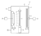
- FIGS. An embodiment of a substrate processing apparatus will be described with reference to FIGS.
- the configuration of the substrate processing apparatus, the configuration of the cleaning chamber provided in the substrate processing apparatus, the operation of the cleaning chamber, and the embodiment will be described in order.
- the substrate processing apparatus 10 includes a carry-in / out chamber 11, a cleaning chamber 12, and a sputter chamber 13, and the carry-in / out chamber 11, the cleaning chamber 12, and the sputter chamber 13 are arranged in one direction. They are arranged in this order along a certain connecting direction.
- a gate valve 14 is located between the carry-in / out chamber 11 and the cleaning chamber 12 and between the cleaning chamber 12 and the sputtering chamber 13.
- Each gate valve 14 is connected to two chambers sandwiching the gate valve 14 in the connecting direction.
- Each chamber includes an exhaust unit 15, and the exhaust unit 15 depressurizes the internal space of the corresponding chamber.
- the exhaust unit 15 evacuates the internal space of the corresponding chamber.
- the substrate processing apparatus 10 includes a transfer unit 16 that extends from the carry-in / out chamber 11 to the sputter chamber 13 along the connecting direction.
- the transport unit 16 transports the tray T that supports the substrate S to be processed in the substrate processing apparatus 10.
- the conveyance part 16 can also fix the tray T in the predetermined position of a connection direction.
- the carry-in / out chamber 11 carries in the tray T supporting the substrate S before processing from the outside of the substrate processing apparatus 10 and carries it out to the cleaning chamber 12. Further, the carry-in / out chamber 11 carries in the tray T supporting the processed substrate S from the cleaning chamber 12 and carries it out of the substrate processing apparatus 10.
- the cleaning chamber 12 includes an anode unit 17 fixed to one inner surface of the substrate processing apparatus 10 and a cathode stage 18 facing the anode unit 17.
- the cleaning chamber 12 cleans the substrate S before processing, and removes deposits attached to the surface of the substrate S.
- the sputter chamber 13 includes a cathode unit 19, and the cathode unit 19 includes a target formed of a predetermined material.
- the sputtering chamber 13 forms a predetermined film on the surface of the substrate S after the cleaning process by sputtering of the target.
- the substrate processing apparatus 10 may include a chamber for performing processing other than the processing performed by the three chambers 11 to 13 described above, or may include a plurality of sputtering chambers 13. Further, the substrate processing apparatus 10 may include at least the cleaning chamber 12 and may not include at least one of the sputtering chamber 13 and the carry-in / out chamber 11.
- the cleaning chamber 12 includes a grounded casing 21 and a gas supply unit 22.
- the cathode stage 18 and the anode unit 17 are disposed in the housing 21.
- the cathode stage 18 is configured to support the substrate S, and a voltage for generating plasma is applied to the cathode stage 18.
- the anode unit 17 includes a first plate 23 and a second plate 24 and is fixed to the housing 21.
- a plurality of first through holes 23a are formed in the first plate 23.
- the gas supply unit 22 flows gas toward the first plate 23.
- the first plate 23 diffuses the gas in the surface direction of the first plate 23 by flowing the gas through the first through hole 23a.
- the second plate 24 is located between the first plate 23 and the cathode stage 18, and a plurality of second through holes 24a (see FIG. 5) larger than the first through holes 23a are formed in the second plate 24.
- the second plate 24 allows the gas that has passed through the first through hole 23a to flow between the second plate 24 and the cathode stage 18 through the second through hole 24a.
- Each second through-hole 24a has a shape in which the plasma emission intensity inside each second through-hole 24a is higher than the plasma emission intensity generated between the second plate 24 and the cathode stage 18. ing.
- the plasma generated between the second plate 24 and the cathode stage 18 is the plasma generated between the anode unit 17 and the cathode stage 18, that is, outside the anode unit 17 (accordingly, each through hole). Plasma generated outside (24a).
- plasma is generated between the anode unit 17 and the cathode stage 18. Is generated. Furthermore, plasma can also be generated inside each second through hole 24 a formed in the second plate 24.
- the cathode stage 18 includes a conductive portion 18a and an insulating portion 18b.
- the conductive portion 18a has a contact surface in contact with the substrate S, and the insulating portion 18b covers a portion other than the contact surface in the conductive portion 18a.
- a power supply 25 for applying a voltage to the cathode stage 18 is connected to the conductive portion 18a.
- the power source 25 is, for example, a high frequency power source, but may be another power source, such as a DC power source.
- the direction in which the anode unit 17 and the cathode stage 18 face each other is a facing direction, and the transport unit 16 is located between the anode unit 17 and the cathode stage 18 in the facing direction.
- the cathode stage 18 is configured to be positioned at the first position and the second position in the facing direction.
- the first position is a position where the contact surface of the conductive portion 18a in the cathode stage 18 is in contact with the substrate S (indicated by a two-dot chain line in FIG. 2)
- the second position is that the cathode stage 18 is in the transport section 16 or transport section 16. This is a position where the tray T supported by is not in contact with (does not interfere with) the tray T.
- a supply port 21a is formed in the casing 21, and a gas supply unit 22 is connected to the supply port 21a.
- the gas supply unit 22 supplies gas into the anode unit 17 from the supply port 21a.
- the gas supply unit 22 is, for example, a mass flow controller connected to a gas cylinder disposed outside the substrate processing apparatus 10.
- the gas supply unit 22 supplies, for example, a rare gas such as argon gas as a gas for generating plasma inside the housing 21.
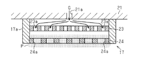
- the anode unit 17 includes a first plate 23 and a second plate 24 that are arranged along the facing direction.
- the supply port 21a, the first plate 23, and the second plate 24 formed in the housing 21 are arranged in this order, and the first plate 23 is located between the supply port 21a and the second plate 24. positioned.
- the distance between the first plate 23 and the second plate 24 is preferably, for example, not less than 10 mm and not more than 50 mm.
- Each first through hole 23a of the first plate 23 passes through the first plate 23 in the opposing direction.
- Each second through hole 24a of the second plate 24 passes through the second plate 24 in the opposing direction.
- the first plate 23 diffuses the gas in the surface direction of the first plate 23 through the plurality of first through holes 23a, and the second plate Flow gas toward 24.
- the second plate 24 causes the gas that has passed through the first through hole 23 a to flow between the second plate 24 and the cathode stage 18 through the plurality of second through holes 24 a.
- the plurality of second through holes 24a of the second plate 24 have a shape such that plasma generated on the surface of the second plate 24 facing the cathode stage 18 enters each second through hole 24a.
- each second through hole 24a overlaps at least one of the plurality of first through holes 23a. According to such an anode unit 17, gas is easily supplied to each of the second through holes 24a, so that plasma is generated inside each second through hole 24a in all or almost all of the plurality of second through holes 24a. Can be generated.
- the anode unit 17 includes a support portion 17a having a cylindrical shape extending in the facing direction.
- the support portion 17 a is an example of a closing portion and a partition portion, and has a first tube end 17 a 1 and a second tube end 17 a 2, and the first tube end 17 a 1 is fixed to the housing 21.
- the support portion 17 a supports the first plate 23 and the second plate 24, and the opening at the second cylinder end 17 a 2 of the support portion 17 a is closed by the second plate 24.
- the first plate 23 is located in the internal space of the anode unit 17 surrounded by the support portion 17a, the second plate 24, and the inner wall of the housing 21.
- the space region between the first plate 23 and the second plate 24 is closed by the support portion 17 a over the entire circumferential direction of the first plate 23.
- the space region between the first plate 23 and the inner wall of the casing 21 in the anode unit 17 (the inner wall where the supply port 21a is located) is also supported by the support portion 17a over the entire circumferential direction of the first plate 23. Closed.
- the support portion 17a functions as a closing portion that closes the periphery of the space region between the first plate 23 and the second plate 24, so that the pressure inside the second through hole 24a can be easily increased. it can. Further, the support portion 17 a functions as a partition portion that partitions the space region between the first plate 23 and the inner wall of the casing 21 in the anode unit 17 from the outside of the anode unit 17. For this reason, the gas supplied toward the first plate 23 easily flows to the space region between the first plate 23 and the second plate 24 through the first through hole 23a. As a result, the pressure in the 2nd through-hole 24a can be raised easily.
- the material for forming the first plate 23, the second plate 24, and the support portion 17a is a metal. And since the 1st cylinder end 17a1 of the support part 17a of the anode unit 17 is being fixed to the housing
- the plurality of first through holes 23 a are regularly arranged in the plane of the first plate 23 in a plan view when the first plate 23 is viewed from the facing direction.
- the plurality of first through holes 23 a may be arranged irregularly in the plane of the first plate 23 in plan view.
- the plurality of first through holes 23 a are regularly arranged in the plane of the first plate 23 along the X direction and the Y direction orthogonal to the X direction.
- the plurality of first through holes 23a are arranged at a predetermined first period P1 along each of the X direction and the Y direction.
- the first period P1 is preferably not less than 1.5 mm and not more than 15 mm, for example.
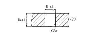
- Each first through hole 23a has a circular hole shape, and the diameter of each first through hole 23a is the first diameter Dia1, and the first diameter Dia1 is preferably not less than 0.5 mm and not more than 5 mm, for example. . If the first diameter Dia1 is not less than 0.5 mm and not more than 5 mm, the plasma P that has entered the second through hole 24a can be prevented from entering the first through hole 23a. It is possible to reduce tolerance.
- the percentage of the total area of the first through holes 23a with respect to the area of the first plate 23 is the first aperture ratio (%), and the first aperture ratio is 5% or more and 50% or less. It is preferable that
- the plurality of second through holes 24 a are regularly arranged in the plane of the second plate 24 in a plan view when the second plate 24 is viewed from the facing direction. Note that the plurality of second through holes 24 a may be irregularly arranged in a plane of the second plate 24 in plan view.
- the plurality of second through holes 24a are regularly arranged in the plane of the second plate 24 along each of the X direction and the Y direction.
- the plurality of second through holes 24a are arranged at a predetermined second period P2 along each of the X direction and the Y direction.
- the second period P2 is preferably 9 mm or more and 60 mm or less, for example.
- Each second through hole 24a has a circular hole shape, and the diameter of each second through hole 24a is the second diameter Dia2.
- the second diameter Dia2 is larger than the first diameter Dia1, for example, 3 mm or more and 20 mm. The following is preferable.
- the second diameter Dia2 is 3 mm or more and 20 mm or less, the ionization efficiency of the gas is increased inside each second through hole 24a, and therefore the density is high around the second plate 24 (around each second through hole 24a). Plasma P can be generated.
- the percentage of the total area of the second through holes 24a with respect to the area of the second plate 24 is the second opening ratio (%), and the second opening ratio is 20% or more and 99% or less. It is preferable that
- the length along the facing direction is the first depth Dep1
- the ratio of the first diameter Dia1 to the first depth Dep1 is first.
- One aspect ratio AR1 is preferably 0.1 or more and 5 or less, for example.
- the length along the facing direction is the second depth Dep2
- the ratio of the second diameter Dia2 to the second depth Dep2 is first. 2 aspect ratio AR2.
- the second aspect ratio AR2 is preferably not less than 0.5 and not more than 15, for example.
- the cathode stage 18 moves from the second position to the first position (position shown in FIG. 8), and the contact surface of the conductive portion 18a contacts the surface of the substrate S.
- the gas supply part 22 supplies argon gas so that the pressure inside the housing
- the supply of argon gas by the gas supply unit 22 may be performed before the movement of the cathode stage 18 or may be started almost simultaneously with the movement of the cathode stage 18.
- the pressure inside the housing 21, for example, preferably at 0.1Pa than 30Pa or less, the power supplied to the cathode stage 18 is the 0.04 W / cm 2 or more 4W / cm 2 or less It is preferable.
- the frequency of the power supplied from the power supply 25 is 1 MHz or more and 40 MHz or less.
- power having a frequency of 100 Hz to 2 MHz may be superimposed on power having a frequency of 1 MHz to 40 MHz. In this case, the power having a frequency of 100 Hz to 2 MHz is 0.02 W. / Cm 2 or more and 0.8 W / cm 2 or less is preferable.
- the argon gas G when the argon gas G is supplied from the supply port 21a into the anode unit 17, the argon gas G passes through the plurality of first through holes 23a formed in the first plate 23. It is diffused along the surface direction of the first plate 23.
- each second through-hole 24a Since the pressure inside each second through-hole 24a is higher than the pressure outside the anode unit 17, it is generated outside the anode unit 17 (between the anode unit 17 and the cathode stage 18) and is inside the second through-hole 24a.
- plasma is also generated in the space between the anode unit 17 and the cathode stage 18 and away from the second plate 24 inside the housing 21. Also in this case, the emission intensity of the plasma formed around the second plate 24 including the plurality of second through holes 24a is increased by generating new plasma in each through hole 24a. And the emission intensity of the plasma generated between the cathode stage 18 and the cathode stage 18.
- the housing 21 may be configured such that a part of the housing 21 functions as an anode, or a configuration in which a metal plate is provided as an anode at a position facing the cathode stage 18. Plasma is generated inside 21.
- a portion in which the pressure of gas for generating plasma is increased does not occur inside the casing 21, and thus a portion in which the plasma emission intensity is increased. Does not occur.
- the emission intensity of the plasma formed around the second plate 24 including the through hole 24 a is generated between the second plate 24 and the cathode stage 18. Higher than the emission intensity of plasma. Therefore, even if a part of the high-frequency voltage is consumed by capacitive coupling between the transport unit 16 and the cathode stage 18, the plasma density in the housing 21 increases. As a result, the sputtering efficiency per power consumption can be increased.
- Example 1 A substrate S having a SiO 2 film formed on the processing surface to be cleaned was prepared, and the processing surface was cleaned using the cleaning chamber 12 described above. The cleaning process was performed under the following conditions. Argon gas was used as a gas for generating plasma in the housing 21.
- the anode unit 17 includes a first plate 23 having a plurality of first through holes 23a having a first diameter Dia1 of 2 mm, and a second plate 24 having a plurality of second through holes 24a having a second diameter Dia2 of 9 mm. It was set as the structure provided. Argon gas was supplied toward the first plate 23 of the anode unit 17 from a supply port 21a formed in the housing.
- Example 1 is the same as Example 1 except that the metal plate disposed at the position facing the cathode stage 18 is subjected to the cleaning process of the substrate S using a cleaning chamber that is used as an anode instead of the anode unit 17 of Example 1 above.
- the substrate S was cleaned under conditions.
- Argon gas was supplied into the housing 21.
- Example 3 The substrate S was cleaned under the same conditions as in Example 1 except that argon gas was supplied into the housing 21 at a position outside the anode unit 17.
- the etching rate of the SiO 2 film was calculated as the removal rate of deposits adhering to the surface of the substrate S.
- the thickness of the SiO 2 film before etching and the thickness of the SiO 2 film after etching are measured, and the value obtained by subtracting the thickness of the SiO 2 film after etching from the thickness of the SiO 2 film before etching is the processing time.
- the etching rate was calculated by dividing. The calculation results of the etching rate are shown in Table 1 below.
- the etching rate in Example 1 was found to be 5.8 mm / min.
- the etching rate in Comparative Example 1 is 3.2 mm / min
- the etching rate in Comparative Example 2 is 2.6 mm / min
- the etching rate in Comparative Example 3 is 3.0 mm / min. Was recognized.
- the anode unit 17 having the second diameter Dia2 in the second plate 24 larger than the first diameter Dia1 in the first plate 23 is used to supply a gas for generating plasma to the first plate 23.
- plasma P can also be generated inside each second through hole 24 a formed in the second plate 24.
- the second diameter Dia2 is 3 mm or more and 20 mm or less, the ionization efficiency of the gas is increased inside the second through hole 24a, and the high-density plasma P can be generated around the second plate 24.
- the plasma P that has entered the second through hole 24a can be prevented from entering the first through hole 23a. Therefore, the plasma resistance required for the first plate 23 can be reduced.
- each 1st through-hole 23a and each 2nd through-hole 24a are not circular hole shape, and may have another shape.
- the through holes 23 a and 24 a may have a square shape in a plan view of the plates 23 and 24.
- the flow path width L which is the maximum length of each through hole 23a, 24a in the plan view of each plate 23, 24, that is, the length of the diagonal line in each through hole 23a, 24a is the first through hole. If it is 23a, what is necessary is just the magnitude
- each through hole 23a, 24a may have a quadrangular shape other than a square shape, or a polygonal shape other than a square shape, for example, a pentagonal shape or a hexagonal shape. And so on.
- each of the through holes 23 a and 24 a may have an elliptical shape in the plan view of each of the plates 23 and 24. Even if it is such a structure, if the flow-path width
- the 1st diameter Dia1 of each 1st through-hole 23a is a magnitude
- the sizes of the one diameter Dia1 may be different from each other.
- size of 2nd diameter Dia2 of each 2nd through-hole 24a may mutually differ. If the first diameter Dai1 of each first through hole 23a is capable of gas diffusion along the surface direction of the first plate 23 and is smaller than the second diameter Dia2 of each second through hole 24a, It may be smaller than 0.5 mm or larger than 5 mm.
- the second diameter Dia2 of each second through hole 24a is such that the plasma emission intensity inside the second through hole 24a is higher than the emission intensity of the plasma generated between the second plate 24 and the cathode stage 18. If it is larger than the first diameter Dia1 of each first through hole 23a, it may be smaller than 3 mm or larger than 20 mm.
- the second through hole 24a may not overlap any of the first through holes 23a.
- the 2nd through-hole 24a does not need to be the shape where the plasma formed between the 2nd plate 24 and the cathode stage 18 enters the inside of the 2nd through-hole 24a.
- the second through hole has a shape in which the plasma emission intensity in the second through hole 24 a is higher than the plasma emission intensity generated between the second plate 24 and the cathode stage 18. If 24a has, the effect according to (1) mentioned above can be acquired.
- both the closed part and the partition part are formed by the same member (support part 17a), but each of the closed part and the partition part may be formed by individual members.
- the support portion 17a may be composed of two members.
- the periphery of the space region between the first plate 23 and the second plate 24 may not be blocked by the blocking portion (supporting portion 17a) but may be opened. Even in such a configuration, as long as the gas supplied through the first through hole 23 a of the first plate 23 flows toward the cathode stage 18 through the second through hole 24 a of the second plate 24, the second through hole 24 a The internal pressure can be higher than the pressure between the second plate 24 and the cathode stage 18. Therefore, the sputtering efficiency per power consumption can be increased.
- the periphery of the space region between the first plate 23 and the inner wall of the casing 21 in the anode unit 17 may be opened without being partitioned by the partitioning portion (supporting portion 17a). Even in such a configuration, as long as the gas supplied through the first through hole 23 a of the first plate 23 flows toward the cathode stage 18 through the second through hole 24 a of the second plate 24, the second through hole 24 a The internal pressure can be higher than the pressure between the second plate 24 and the cathode stage 18. Therefore, the sputtering efficiency per power consumption can be increased.
- the cathode stage 18 may be fixed at a predetermined position in the casing 21 as long as it does not interfere with the conveyance of the tray T. While the position of the cathode stage 18 in the casing 21 is fixed, the transport unit 16 moves along the facing direction in which the anode unit 17 and the cathode stage 18 face each other, so that the position of the tray T is set to the first position. You may change between a position and a 2nd position. In this case, the first position and the second position are different positions in the facing direction.
- the first position is a position where the tray 16 and the cathode stage 18 do not interfere with each other, and the transport unit 16 can transport the tray T
- the second position is the position where the cathode stage 18 and the substrate S are located. It is a position to touch.
- the cathode stage 18 is formed so that a portion of the conductive portion 18a that contacts the substrate S is exposed from the insulating portion 18b. If the voltage can be applied to the substrate S, the entire conductive portion 18a is formed. May be covered by the insulating portion 18b.
- the substrate processing apparatus 10 may be an apparatus that performs a cleaning process on the substrate S in a state where the tray T is arranged substantially in the horizontal direction.
- the transfer unit 16 arranges the tray T along the substantially horizontal direction across the plurality of chambers 11 to 13, for example. You may convey in the state which carried out.
- the substrate processing apparatus 10 includes only the carry-in / out chamber 11 and the cleaning chamber 12, the carry-in / out chamber 11 receives the tray T from the outside of the carry-in / out chamber 11 and conveys the tray T to the cleaning chamber 12.
- a transfer robot may be provided.
- the tray T may be omitted.
Landscapes
- Chemical & Material Sciences (AREA)
- Engineering & Computer Science (AREA)
- Physics & Mathematics (AREA)
- Plasma & Fusion (AREA)
- Analytical Chemistry (AREA)
- Chemical Kinetics & Catalysis (AREA)
- Materials Engineering (AREA)
- Mechanical Engineering (AREA)
- Metallurgy (AREA)
- Organic Chemistry (AREA)
- Plasma Technology (AREA)
- Physical Vapour Deposition (AREA)
Abstract
Description
一実施形態において、上記基板処理装置は、前記第1プレートと前記アノードユニット内における前記筐体の内壁との間の空間領域を、前記第1プレートの周方向の全体にわたり前記アノードユニットの外部から区画する区画部をさらに備えることが好ましい。
この構成によれば、第2貫通孔の内部において密度の高いプラズマが生成されやすくなる。
この構成によれば、第2貫通孔に入り込んだプラズマが第1貫通孔にまで入り込むことが抑えられるため、第1プレートに必要とされるプラズマ耐性を軽減することが可能でもある。
図1を参照して基板処理装置の構成を説明する。
図1が示すように、基板処理装置10は、搬出入チャンバ11、洗浄チャンバ12、および、スパッタチャンバ13を備え、搬出入チャンバ11、洗浄チャンバ12、および、スパッタチャンバ13は、1つの方向である連結方向に沿ってこの順に並んでいる。
図2から図7を参照して洗浄チャンバ12の構成を説明する。
図2が示すように、洗浄チャンバ12は、接地された筐体21およびガス供給部22を備えている。カソードステージ18およびアノードユニット17は、筐体21内に配置されている。カソードステージ18は、基板Sを支持するように構成され、カソードステージ18には、プラズマを生成するための電圧が印加される。
図3が示すように、アノードユニット17は、対向方向に沿って並ぶ第1プレート23と第2プレート24とを備えている。対向方向において、筐体21に形成された供給ポート21a、第1プレート23、および、第2プレート24がこの順で並び、第1プレート23は、供給ポート21aと第2プレート24との間に位置している。対向方向において、第1プレート23と第2プレート24との間の距離は、例えば、10mm以上50mm以下であることが好ましい。
こうしたアノードユニット17によれば、各第2貫通孔24aに対してガスが供給されやすくなるため、複数の第2貫通孔24aの全てもしくはほとんど全てで、各第2貫通孔24aの内部にプラズマを生成することができる。
第1径Dia1が0.5mm以上5mm以下であれば、第2貫通孔24aに入り込んだプラズマPが第1貫通孔23aにまで入り込むことが抑えられるため、第1プレート23に必要とされるプラズマ耐性を軽減することが可能である。
図8および図9を参照して洗浄チャンバ12の作用を説明する。
図8が示すように、洗浄チャンバ12において基板Sの洗浄処理が行われるときには、まず、搬送部16が、搬出入チャンバ11から洗浄チャンバ12に搬入したトレイTをアノードユニット17と対向する処理位置まで搬送し、処理位置にてトレイTの位置を固定する。なお、トレイTが洗浄チャンバ12内に搬入されるとき、筐体21の内部は、排気部15によって所定の圧力まで減圧されている。
以下、実施例と種々の比較例について説明する。以下では、理解を容易にするために、上記実施形態の構成と類似の構成には同様の符号を付して説明する。
洗浄処理の対象となる処理面にSiO2膜が形成された基板Sを準備し、上述した洗浄チャンバ12を用いて、処理面を洗浄した。洗浄処理は、以下の条件で行った。なお、筐体21内にプラズマを生成するためのガスとしてアルゴンガスを用いた。
・電力 0.6W/cm2(13.56MHz)
アノードユニット17は、第1径Dia1が2mmである複数の第1貫通孔23aを有する第1プレート23と、第2径Dia2が9mmである複数の第2貫通孔24aを有する第2プレート24を備える構成とした。アルゴンガスは、筐体に形成された供給ポート21aからアノードユニット17の第1プレート23に向けて供給した。
カソードステージ18と対向する位置に配置された金属板を、上記実施例1のアノードユニット17に代えてアノードとして使用する洗浄チャンバを用いて基板Sの洗浄処理を行う以外は、実施例1と同じ条件で基板Sの洗浄処理を行った。なお、アルゴンガスは、筐体21の内部に供給した。
上記実施例1のアノードユニット17において、第2プレート24の各第2貫通孔24aの第2径Dia2が2mmである以外は、実施例1と同じ条件で基板Sの洗浄処理を行った。
アノードユニット17の外部の位置でアルゴンガスを筐体21の内部に供給する以外は、実施例1と同じ条件で基板Sの洗浄を行った。
実施例1および比較例1から比較例3の各々について、基板Sの表面に付着した付着物の除去速度として、SiO2膜のエッチング速度を算出した。エッチング前のSiO2膜の厚さと、エッチング後のSiO2膜の厚さとを測定し、エッチング前のSiO2膜の厚さからエッチング後のSiO2膜の厚さを引いた値を処理時間で除算することによって、エッチング速度を算出した。エッチング速度の算出結果を以下の表1に示す。

(1)第1プレート23を介して第2プレート24にガスが供給されている状態でカソードステージ18に電圧が印加されると、アノードユニット17とカソードステージ18との間に生成されるプラズマPに加え、第2プレート24に形成された各第2貫通孔24aの内部にもプラズマPを生成することができる。これにより、筐体21内におけるプラズマPの密度が高まり、基板Sに向けて引きつけられる荷電粒子の密度も高まる。結果として、基板Sに付着した付着物を除去する速度が高まる。
・各第1貫通孔23aおよび各第2貫通孔24aは円形孔状ではなく、他の形状を有してもよい。
・各第1貫通孔23aの第1径Dai1は、第1プレート23の面方向に沿ってガスの拡散が可能であり、かつ、各第2貫通孔24aの第2径Dia2よりも小さければ、0.5mmよりも小さくてもよいし、5mmよりも大きくてもよい。
・第2貫通孔24aは、第2プレート24とカソードステージ18との間に形成されたプラズマが、第2貫通孔24aの内部に入り込む形状でなくてもよい。こうした構成であっても、第2貫通孔24aの内部におけるプラズマの発光強度が、第2プレート24とカソードステージ18との間に生成されるプラズマの発光強度よりも高められる形状を第2貫通孔24aが有していれば、上述した(1)に準じた効果を得ることはできる。
・筐体21内におけるカソードステージ18の位置が固定されている一方で、アノードユニット17とカソードステージ18とが向かい合う対向方向に沿って搬送部16が移動することで、トレイTの位置を第1位置と第2位置との間で変えてもよい。この場合、第1位置と第2位置とは、対向方向において互いに異なる位置である。このうち、第1位置は、トレイTとカソードステージ18とが干渉せずに搬送部16がトレイTを搬送することが可能な位置であり、第2位置は、カソードステージ18と基板Sとが接する位置である。
Claims (5)
- 接地された筐体と、
前記筐体内に位置するとともに基板を支持するように構成され、プラズマを生成するための電圧が印加されるカソードステージと、
前記筐体に固定されたアノードユニットであって、
前記筐体内に位置するとともに複数の第1貫通孔を含む第1プレートと、
前記第1プレートと前記カソードステージとの間に位置するとともに前記第1貫通孔よりも大きい複数の第2貫通孔を含む第2プレートと、
を含むアノードユニットと、
前記第1プレートに向けてガスを供給するガス供給部と、を備え、
前記第1プレートは、前記複数の第1貫通孔を通じて前記ガスを流すことによって、前記ガスを前記第1プレートの面方向へ拡散させるように構成され、
前記第2プレートは、前記第1貫通孔を通過した前記ガスを、前記複数の第2貫通孔を通じて前記第2プレートと前記カソードステージとの間に流すように構成され、
前記複数の第2貫通孔は、各第2貫通孔の内部におけるプラズマの発光強度を前記第2プレートと前記カソードステージとの間に生成されるプラズマの発光強度よりも高める形状を有している、
基板処理装置。 - 前記第2プレートは、前記第1プレートと対向する位置に配置され、
前記第1プレートと前記第2プレートとの間の空間領域を前記第1プレートの周方向の全体にわたり閉じる閉塞部をさらに備える
請求項1に記載の基板処理装置。 - 前記第1プレートと前記アノードユニット内における前記筐体の内壁との間の空間領域を、前記第1プレートの周方向の全体にわたり前記アノードユニットの外部から区画する区画部をさらに備える
請求項1または2に記載の基板処理装置。 - 前記複数の第2貫通孔の各々は円形孔状に形成され、3mm以上20mm以下の直径を有する、
請求項1から3のいずれか一項に記載の基板処理装置。 - 前記複数の第1貫通孔の各々は円形孔状に形成され、0.5mm以上5mm以下の直径を有する、
請求項4に記載の基板処理装置。
Priority Applications (4)
| Application Number | Priority Date | Filing Date | Title |
|---|---|---|---|
| US15/542,861 US10490390B2 (en) | 2015-06-29 | 2016-06-08 | Substrate processing device |
| CN201680004832.8A CN107109618B (zh) | 2015-06-29 | 2016-06-08 | 基板处理装置 |
| JP2017526255A JP6483259B2 (ja) | 2015-06-29 | 2016-06-08 | 基板処理装置 |
| KR1020177017930A KR101920249B1 (ko) | 2015-06-29 | 2016-06-08 | 기판 처리 장치 |
Applications Claiming Priority (2)
| Application Number | Priority Date | Filing Date | Title |
|---|---|---|---|
| JP2015129700 | 2015-06-29 | ||
| JP2015-129700 | 2015-06-29 |
Publications (1)
| Publication Number | Publication Date |
|---|---|
| WO2017002564A1 true WO2017002564A1 (ja) | 2017-01-05 |
Family
ID=57608763
Family Applications (1)
| Application Number | Title | Priority Date | Filing Date |
|---|---|---|---|
| PCT/JP2016/067108 Ceased WO2017002564A1 (ja) | 2015-06-29 | 2016-06-08 | 基板処理装置 |
Country Status (6)
| Country | Link |
|---|---|
| US (1) | US10490390B2 (ja) |
| JP (1) | JP6483259B2 (ja) |
| KR (1) | KR101920249B1 (ja) |
| CN (1) | CN107109618B (ja) |
| TW (1) | TWI670382B (ja) |
| WO (1) | WO2017002564A1 (ja) |
Families Citing this family (2)
| Publication number | Priority date | Publication date | Assignee | Title |
|---|---|---|---|---|
| CN114438441B (zh) * | 2021-12-30 | 2023-11-21 | 广东鼎泰高科技术股份有限公司 | 一种等离子体增强清洗装置及清洗方法 |
| CN114453345B (zh) * | 2021-12-30 | 2023-04-11 | 广东鼎泰高科技术股份有限公司 | 一种等离子体清洗系统 |
Citations (2)
| Publication number | Priority date | Publication date | Assignee | Title |
|---|---|---|---|---|
| JP2009010101A (ja) * | 2007-06-27 | 2009-01-15 | Tokyo Electron Ltd | 基板処理装置およびシャワーヘッド |
| JP2012216823A (ja) * | 2011-03-31 | 2012-11-08 | Tokyo Electron Ltd | ガス吐出機能付電極およびプラズマ処理装置 |
Family Cites Families (9)
| Publication number | Priority date | Publication date | Assignee | Title |
|---|---|---|---|---|
| JPH02134814A (ja) * | 1988-11-16 | 1990-05-23 | Oki Electric Ind Co Ltd | プラズマcvd法による薄膜の製造方法及びその装置 |
| HUE035964T2 (hu) * | 2006-10-27 | 2018-06-28 | Oerlikon Surface Solutions Ag Pfaeffikon | Eljárás és berendezés további kezelésre kerülõ, tisztított szubsztrátok vagy tiszta szubsztrátok gyártására |
| US20110272099A1 (en) * | 2008-05-02 | 2011-11-10 | Oerlikon Trading Ag, Truebbach | Plasma processing apparatus and method for the plasma processing of substrates |
| JP5135106B2 (ja) * | 2008-07-31 | 2013-01-30 | 富士フイルム株式会社 | 成膜装置および成膜方法、並びに、液体吐出装置 |
| KR101062452B1 (ko) | 2008-12-30 | 2011-09-05 | 엘아이지에이디피 주식회사 | 플라즈마 처리장치 |
| US9184028B2 (en) * | 2010-08-04 | 2015-11-10 | Lam Research Corporation | Dual plasma volume processing apparatus for neutral/ion flux control |
| US9082593B2 (en) | 2011-03-31 | 2015-07-14 | Tokyo Electron Limited | Electrode having gas discharge function and plasma processing apparatus |
| JP6022373B2 (ja) | 2013-02-04 | 2016-11-09 | 株式会社アルバック | 薄型基板処理装置 |
| JP6113624B2 (ja) * | 2013-10-11 | 2017-04-12 | 株式会社荏原製作所 | 基板処理装置および基板処理方法 |
-
2016
- 2016-06-08 KR KR1020177017930A patent/KR101920249B1/ko active Active
- 2016-06-08 CN CN201680004832.8A patent/CN107109618B/zh active Active
- 2016-06-08 WO PCT/JP2016/067108 patent/WO2017002564A1/ja not_active Ceased
- 2016-06-08 JP JP2017526255A patent/JP6483259B2/ja active Active
- 2016-06-08 US US15/542,861 patent/US10490390B2/en active Active
- 2016-06-20 TW TW105119283A patent/TWI670382B/zh active
Patent Citations (2)
| Publication number | Priority date | Publication date | Assignee | Title |
|---|---|---|---|---|
| JP2009010101A (ja) * | 2007-06-27 | 2009-01-15 | Tokyo Electron Ltd | 基板処理装置およびシャワーヘッド |
| JP2012216823A (ja) * | 2011-03-31 | 2012-11-08 | Tokyo Electron Ltd | ガス吐出機能付電極およびプラズマ処理装置 |
Also Published As
| Publication number | Publication date |
|---|---|
| CN107109618B (zh) | 2019-10-22 |
| TWI670382B (zh) | 2019-09-01 |
| US20180012734A1 (en) | 2018-01-11 |
| TW201715058A (zh) | 2017-05-01 |
| KR20170093872A (ko) | 2017-08-16 |
| CN107109618A (zh) | 2017-08-29 |
| US10490390B2 (en) | 2019-11-26 |
| JPWO2017002564A1 (ja) | 2017-11-02 |
| JP6483259B2 (ja) | 2019-03-13 |
| KR101920249B1 (ko) | 2018-11-20 |
Similar Documents
| Publication | Publication Date | Title |
|---|---|---|
| JP5659425B2 (ja) | 負イオンプラズマを生成する処理システムおよび中性ビーム源 | |
| JP5154124B2 (ja) | プラズマ処理装置 | |
| KR102576482B1 (ko) | 플라즈마 생성 장치 | |
| TW201907755A (zh) | 藉由直流偏壓調節之顆粒產生抑制器 | |
| JP6544902B2 (ja) | プラズマ処理装置 | |
| JP7158308B2 (ja) | プラズマ処理装置及びプラズマ処理方法 | |
| JP4945566B2 (ja) | 容量結合型磁気中性線プラズマスパッタ装置 | |
| TW201941253A (zh) | 電漿處理裝置 | |
| KR101977819B1 (ko) | 타겟 어셈블리 | |
| JP6483259B2 (ja) | 基板処理装置 | |
| JP4943879B2 (ja) | プラズマ処理装置 | |
| KR101926676B1 (ko) | 타겟 어셈블리 | |
| CN102224561B (zh) | 射频溅射配置 | |
| JP5678116B2 (ja) | 蓋部品、処理ガス拡散供給装置、及び基板処理装置 | |
| JP6509553B2 (ja) | スパッタリング装置 | |
| US10184171B2 (en) | Sputtering apparatus and method thereof | |
| JP2014070275A5 (ja) | ||
| JP6511813B2 (ja) | プラズマ処理電極およびcvd電極 | |
| KR20160071452A (ko) | 절연물 타겟 | |
| JP2020523759A (ja) | プラズマ処理装置 | |
| KR20230087956A (ko) | 표면 증착의 균일도 향상을 위한 스퍼터링 장치 | |
| KR20150077522A (ko) | 스퍼터링 장치 | |
| JP2018135575A (ja) | スパッタリング装置 | |
| JP2017088973A (ja) | プラズマスパッタ装置 |
Legal Events
| Date | Code | Title | Description |
|---|---|---|---|
| 121 | Ep: the epo has been informed by wipo that ep was designated in this application |
Ref document number: 16817673 Country of ref document: EP Kind code of ref document: A1 |
|
| ENP | Entry into the national phase |
Ref document number: 20177017930 Country of ref document: KR Kind code of ref document: A |
|
| WWE | Wipo information: entry into national phase |
Ref document number: 15542861 Country of ref document: US |
|
| ENP | Entry into the national phase |
Ref document number: 2017526255 Country of ref document: JP Kind code of ref document: A |
|
| NENP | Non-entry into the national phase |
Ref country code: DE |
|
| 122 | Ep: pct application non-entry in european phase |
Ref document number: 16817673 Country of ref document: EP Kind code of ref document: A1 |