WO2016209666A2 - Hybrid metal-graphene terahertz optoelectronic system with tunable plasmonic resonance and method of fabrication - Google Patents
Hybrid metal-graphene terahertz optoelectronic system with tunable plasmonic resonance and method of fabrication Download PDFInfo
- Publication number
- WO2016209666A2 WO2016209666A2 PCT/US2016/037393 US2016037393W WO2016209666A2 WO 2016209666 A2 WO2016209666 A2 WO 2016209666A2 US 2016037393 W US2016037393 W US 2016037393W WO 2016209666 A2 WO2016209666 A2 WO 2016209666A2
- Authority
- WO
- WIPO (PCT)
- Prior art keywords
- graphene
- plasmon
- plasmonic
- layer
- optoelectronic structure
- Prior art date
- Legal status (The legal status is an assumption and is not a legal conclusion. Google has not performed a legal analysis and makes no representation as to the accuracy of the status listed.)
- Ceased
Links
Classifications
-
- H—ELECTRICITY
- H10—SEMICONDUCTOR DEVICES; ELECTRIC SOLID-STATE DEVICES NOT OTHERWISE PROVIDED FOR
- H10F—INORGANIC SEMICONDUCTOR DEVICES SENSITIVE TO INFRARED RADIATION, LIGHT, ELECTROMAGNETIC RADIATION OF SHORTER WAVELENGTH OR CORPUSCULAR RADIATION
- H10F30/00—Individual radiation-sensitive semiconductor devices in which radiation controls the flow of current through the devices, e.g. photodetectors
- H10F30/10—Individual radiation-sensitive semiconductor devices in which radiation controls the flow of current through the devices, e.g. photodetectors the devices being sensitive to infrared radiation, visible or ultraviolet radiation, and having no potential barriers, e.g. photoresistors
-
- H—ELECTRICITY
- H01—ELECTRIC ELEMENTS
- H01G—CAPACITORS; CAPACITORS, RECTIFIERS, DETECTORS, SWITCHING DEVICES, LIGHT-SENSITIVE OR TEMPERATURE-SENSITIVE DEVICES OF THE ELECTROLYTIC TYPE
- H01G9/00—Electrolytic capacitors, rectifiers, detectors, switching devices, light-sensitive or temperature-sensitive devices; Processes of their manufacture
- H01G9/20—Light-sensitive devices
- H01G9/2045—Light-sensitive devices comprising a semiconductor electrode comprising elements of the fourth group of the Periodic Table with or without impurities, e.g. doping materials
-
- G—PHYSICS
- G01—MEASURING; TESTING
- G01N—INVESTIGATING OR ANALYSING MATERIALS BY DETERMINING THEIR CHEMICAL OR PHYSICAL PROPERTIES
- G01N21/00—Investigating or analysing materials by the use of optical means, i.e. using sub-millimetre waves, infrared, visible or ultraviolet light
- G01N21/17—Systems in which incident light is modified in accordance with the properties of the material investigated
- G01N21/25—Colour; Spectral properties, i.e. comparison of effect of material on the light at two or more different wavelengths or wavelength bands
- G01N21/31—Investigating relative effect of material at wavelengths characteristic of specific elements or molecules, e.g. atomic absorption spectrometry
- G01N21/35—Investigating relative effect of material at wavelengths characteristic of specific elements or molecules, e.g. atomic absorption spectrometry using infrared light
- G01N21/3581—Investigating relative effect of material at wavelengths characteristic of specific elements or molecules, e.g. atomic absorption spectrometry using infrared light using far infrared light; using Terahertz radiation
-
- G—PHYSICS
- G01—MEASURING; TESTING
- G01N—INVESTIGATING OR ANALYSING MATERIALS BY DETERMINING THEIR CHEMICAL OR PHYSICAL PROPERTIES
- G01N21/00—Investigating or analysing materials by the use of optical means, i.e. using sub-millimetre waves, infrared, visible or ultraviolet light
- G01N21/17—Systems in which incident light is modified in accordance with the properties of the material investigated
- G01N21/25—Colour; Spectral properties, i.e. comparison of effect of material on the light at two or more different wavelengths or wavelength bands
- G01N2021/258—Surface plasmon spectroscopy, e.g. micro- or nanoparticles in suspension
-
- Y—GENERAL TAGGING OF NEW TECHNOLOGICAL DEVELOPMENTS; GENERAL TAGGING OF CROSS-SECTIONAL TECHNOLOGIES SPANNING OVER SEVERAL SECTIONS OF THE IPC; TECHNICAL SUBJECTS COVERED BY FORMER USPC CROSS-REFERENCE ART COLLECTIONS [XRACs] AND DIGESTS
- Y02—TECHNOLOGIES OR APPLICATIONS FOR MITIGATION OR ADAPTATION AGAINST CLIMATE CHANGE
- Y02E—REDUCTION OF GREENHOUSE GAS [GHG] EMISSIONS, RELATED TO ENERGY GENERATION, TRANSMISSION OR DISTRIBUTION
- Y02E10/00—Energy generation through renewable energy sources
- Y02E10/50—Photovoltaic [PV] energy
- Y02E10/542—Dye sensitized solar cells
Definitions
- the present invention is directed to optoelectronics, and in particular, to graphene-based large area terahertz optoelectronic systems with an increased absorption efficiency and tunable operational parameters.
- the present invention is directed to optoelectronic devices with the perfomiance enhanced by a unique type of plasmon resonance
- the present invention is directed to large area terahertz optoelectronic systems (photodetectors, filters, modulators, and oscillators) with improved operational parameters attained through utilizing a tunable graphene- enabled plasmonic resonance in a hybrid graphene-metal design composed of a periodic array of narrow graphene channels formed in a metal (conductive) layer which is patterned on a continuous graphene layer.
- graphene acts as a gate-tunable inductor, while the metal acts as a capacitive reservoir for charge accumulation.
- the present invention also is directed to hybrid metal -graphene based terahertz photodetectors exhibiting strong absorption and a fast response, which are tunable over a broad range of frequency in the THz (terahertz) spectrum by changing the dimensions of graphene micro-ribbons and/or the carrier density, which are amenable to fabrication of arrays for large-area photodetectors.
- the present invention is directed to optoelectronic systems exhibiting anomalously high resonant absorption (or transmission) when sub- wavelength graphene-filied apertures are introduced into a conductive layer.
- Plasmonic resonances in finite-size two-dimensional conductors are able to couple strongly with Tiiz radiation and can be tuned by application of a gate voltage, as presented in Ju Long, et al,, "Graphene Plasmonics for Tunable Terahertz Metamaterials", Nature Nanotec, 6, 630-634 (201 1), and Yan Hugen, et al. "Tunable infrared Plasmonic Devices using Graphene/insulator Stacks", Nature Nanotec, 7, 330-345 (2012). These features are attractive for a variety of electrically tunable terahertz devices, such as, for example, detectors, emitters, filters, and modulators.
- graphene is a particularly attractive plasmonic medium due to its electrical and thermal properties at room temperature.
- Particularly promising is terahertz (THz) photodetection, in which graphene-based devices may offer significant advantages over existing technology in terms of speed and sensitivity.
- THz terahertz
- plasmonic resonances occur in isolated graphene elements, where the isolating charge accumulates at opposite edges of a sub-wavelength graphene element. Integrating such a plasmonic element with an antenna, metamaterial, or electrical contact greatly increases the range of potential applications. However, a conductive boundary inhibits the accumulation of charge at the edges which was previously thought to prevent the plasmonic resonance.
- graphene supports terahertz two- dimensional plasma waves; subwavelength charge density oscillations connected with electromagnetic fields that are tightly localized near the graphene sheet. When these waves are confined to finite-sized graphene. plasmon resonances emerge that are characterized by alternating charge accumulation at the opposing edges of the graphene.
- the resonant frequency of such a structure depends on both the size and the surface charge density and can be electrostatically tuned throughout the terahertz range by applying a gate voltage,
- Another approach contemplates placing a photodetector in a micro cavity, which resonates at a selected frequency.
- This approach can enhance absorption, but to date this has been demonstrated only at near-infrared wavelengths and can be cumbersome for long wavelength THz radiation.
- Coupling the detector to an antenna is a viable approach for frequencies up to the low ⁇ , but there are few demonstrations of antenna-coupled graphene devices, and the approach is applicable only to devices whose size is much smaller than the wavelength.
- the mobility ⁇ exceeds 50.000 cm 2 /V-s, uniquely high resonant transmission is attained in a high- mobility graphene which reaches nearly 100% resonant THz transmission beneficial for near perfect tunable THz filters or modulators.
- an object of the present invention is to provide a hybrid metal graphene based optoelectronic device where a large resonant absorption is attained in a low-mobility graphene ( ⁇ 1000 cmVv-s), with a peak of resonant absorption approaching 100% which is ideal for graphene-based THz detectors.
- the present invention is related to a hybrid metal -graphene based terahertz optoelectronic system with tunable plasmonic resonance which comprises a first periodic array of conductive stripes formed above a substrate, and a layer of graphene sandwiched between the substrate and the first, periodic array of the conductive stripes.
- the layer of graphene comprises a second periodic array of graphene channels confined in the respective gaps between the neighboring conductive stripes. The width of each of the conductive stripes exceeds a width of each of the graphene channels.
- the subject plasmon-enhanced terahertz graphene-based optoelectronic structure further includes an electrolyte layer positioned atop and enveloping the first periodic array of conductive stripes and the second periodic array of the graphene channels.
- the plasmon-enhanced terahertz graphene-based optoelectronic structure further includes a source terminal and a drain terminal coupled to respective conductive stripes of the first periodic array, and a gate terminal coupled between the electrolyte layer and the layer of graphene.
- a source of gate voltage V g is applied between the source and gate terminals to tune operational parameters of the optoelectronic structure.
- the subject plasmon-enhanced graphene-based optoelectronic structure further includes a source of a linearly polarized light which is directed incident on the graphene channels.
- the light is polarized substantially perpendicular to the graphene channels.
- the polarized light excites transverse plasmon in the graphene channels.
- the plasmon resonance frequency and strength of the resonance absorption is controlled through controlling the gate voltage V g to tune carriers density in the graphene layer.
- the plasmon resonance frequency and strength of the resonance absorption is controlled through adjusting the geometrical features of the structure, such as the width of the conductive stripes, and/or the width of the graphene channels.
- each graphene channel falls in a sub-micron range, and may range from 100 nm to few microns depending on the desired plasmon resonance frequency.
- a ratio AJw between a period ⁇ of the first array of conductive stripes and the width w of each graphene channel exceeds 10, and may be greater than 20.
- the period ⁇ of the array of conductive stripes ranges from 1 ⁇ to 9 ⁇ .
- the plasmon resonance frequency and strength of the resonance absorption is controlled in the subject optoelectronic system by controlling gate voltage V g to tune carrier density in the graphene layer.
- the ratio AJw of the period ⁇ of the first array of conductive stripes to the width w of each graphene channel is chosen to be approximately 20: 1 when the mobility of carriers in the graphene layer is 1,000 cmW-s to achieve the maximal absorption in graphene for carrier dens: ity of 1.5 x 10" ⁇ " ⁇ .
- the optimal AJw for achieving the maximal absorption can be calculated using tan equivalent circuit model.
- the subject plasmon-enhanced terahertz graphene-based optoelectronic structure acts as a tunable photodetector with a uniquely high absorption (approximating 100%) when the mobility of carriers in the graphene layer is as low as approximately 1000 cm V-s,
- the subject plasmon-enhanced terahertz graphene-based optoelectronic structure acts as a tunable filter or modulator when the graphene mobility is high (over 50,000 cm /V-s) and is tuned through application of the controllable V g ,
- the present invention is directed to a method of fabrication of a plasmon-enhanced terahertz hybrid metal graphene-based optoelectronic system, which is accomplished through the sequence of the following steps:
- the subject method continues with the steps of:
- a source of gate voltage is coupled between the graphene and the gate terminal
- a ratio of a period ⁇ of the periodic array of the metallic stripes to a width w of each graphene channel exceeds 10.
- These new plasmon modes offer the potential to incorporate a tunable plasmonic channel into a device with electrical contacts, which is an important step toward practical graphene terahertz optoelectronics.
- an anomalously high resonant absorption (or transmission) has been demonstrated when subwavelength graphene-filled apertures are introduced into an otherwise conductive layer.
- These tunable plasmon resonances are essential yet missing ingredients needed for terahertz filters, oscillators, detectors, and modulators.
- FIG, 1 A is an SEM (Scanning Electron Microscope) image of a small part of the topology of a subject hybrid metal-graphene based optoelectronic system;
- FIG. IB is a side view of the subject hybrid metal-graphene based optoelectronic system showing the applied controllable gate voltage V g and an incident electromagnetic wave polarized perpendicular to the graphene channels, as well as the Reflected (R) and Transmitted (T) portions of the radiation;
- FIG. 2A is a schematic representation of the subject metal on graphene grating
- FIG. 2B is a schematic representation of the array of isolated (no metal contact) graphene ribbons
- FIG. 2C is a diagram representative of the graphene absorption (A G ) under electromagnetic wave excitation-of-metal on graphene gratings with different periods ( ⁇ ) as a function of the frequency /for structure shown in FIG. 2A;
- FIG. 2D is a diagram representative of the graphene absorption (AQ) of an array of isolated graphene ribbons shown in FIG. 2B with the same graphene parameters as in the structure shown in FIG. 2A;
- FIGS. 2E and 2F are representative of charge density profiles at the plasmon frequency for metal-graphene structure of FIG. 2A and the graphene ribbons of FIG. 2B, respectively;
- FiG, 3A is a schematic representation of the 4-terminal circuit model for the subject hybrid metal on graphene structure;
- FIG. 3B is a simplified circuit model (no input waves) which is used to determine resonant (plasrnon) frequency and the damping rate;
- FIG. 4A is a diagram representative of the measured transmission (T) for different graphene carrier densities tuned by applying a gate voltage V g vs. the frequency;
- FIG. 4B is a diagram representative of the measured reflection (R) of the subject device for different carrier densities normalized to the lowest carrier density data versus frequency;
- FIG, 4C is a diagram representative of the controlling capabilities of the subject optoelectronic device for the absorption (relative to the lowest carrier density) by electrically tuning the graphene carrier density;
- FIG. 4D is a diagraph representative of the finite element calculations of Transmission for different carrier densities
- FIG. 4E is a diagram representative of the finite element calculations of the normalized reflection for different carrier densities:
- FIG, 5B is a diagram representative of the plasmon resonance width as a function of graphene mobility
- FIG. 5C is a diagram representative of the transmission through the metal- graphene grating for different carrier density levels
- FIG. 5D is a diagram representative of the absorption AQ at the higher order plasmon resonance for different graphene mobilities
- FIG. 6 is a schematic diagram of a unit cell of the subject periodic structure:
- FIGS. 7 A and 7B are diagrams representative of Transmission and Reflection. respectively, for different array periods computed by mil-wave finite element calculations;
- FIGS. 7C and 7D are diagrams of Transmission and Reflection for different periods of the subject structure, respectively, calculated by the circuit model shown in FIG, 3A;
- FIGS. 9 A - 9F are representative of the sequence of manufacturing steps for fabrication of the subject metal-graphene based optoelectronic structure. DETAILED DESCRIPTION OF THE PREFERRED EMBODIMENTS
- a new type of plasmon resonance that occurs when graphene is connected to a metal has been discovered.
- the new plasmon modes offer the potential to incorporate a tunable plasmonic channel into a device with electrical contacts, which is an important step toward fabrication of practical graphene terahertz optoelectronics.
- Anomalously high resonant absorption (or transmission) has been demonstrated when subwavelength graphene-filled apertures are introduced into an otherwise conductive layer.
- These tunable plasmon resonances are important ingredients needed for terahertz filters, oscillators, detectors, and modulators.
- High mobility graphene (such as, for example, 50,000 cm /V-s) is envisioned to produce a tunable resonance peak in transmission that approaches 100%, which is ideal for THz modulators and tunable bandpass filters.
- the metal-graphene based plasmon- enhanced terahertz (THz) optoelectronic structure 10 is formed on a substrate 12, for example, an SiC substrate.
- the subject optoelectronic structure 10 includes a continuous graphene layer 14 and a conductive (metallic) layer 16 formed (deposited) on the graphene layer 14 and patterned to form a periodic array of stripes (or strips) 18 of the conductive (for example, Au) material separated by narrow slots (gaps) 20 between the metal stripes 18 with exposed graphene layer portions 22, further referred to herein as graphene channels or graphene lines.
- the subject optoelectronic structure 10 constitutes a periodic array of sub-micron graphene lines (also referred to herein as graphene channels) 22 defined between conductive stripes 18.
- Geometrical parameters of the periodic arrays of the conductive stripes and the graphene channels are important for the operation of the subject structure, as will be detailed in ftirther paragraphs, and are controlled to tune the plasmon resonance modes in the subject structure.
- the period ⁇ of the periodic array of conductive stripes 18 must exceed the width w of the graphene channels, i.e., ⁇ » w.
- the ratio of AJw may exceed 10, and may be as high as 20, or higher.
- the width of the metal stripes 18 ranges in a ⁇ diapason, and in one of the examples, may approximate 7 ⁇ .
- the width w of the graphene lines 22 falls in a sub-micron range, and, in exemplary embodiments, can be between approximately 100 nm and few micrometers.
- a layer of an electrolyte 24 is formed on the top of the metal grating, in one of the embodiments, when the optoelectronic structure 10 is formed as a photodetecior, the outermost metal stripes form the source terminal 26 and a drain terminal 28.
- a gate terminal 30 is coupled to the graphene layer 14 via the electrolyte layer 24, as shown in FIG. IB.
- a gate voltage V g is applied between the graphene layer 1 and the gate terminal 30.
- the total output signal Vout is the integral of the potential gradient over the device length, in addition, the graphene acts as a gate-tunable inductor in the structure 10 variable by the application of the controllable gate voltage V g , and the metal stripes 18 act as a capacitive reservoir for charge accumulation.
- the plasmon mode in the optoelectronic structure 10 shows strong coupling to the incident terahertz radiation 32, so that an extremely strong absorption in graphene layer 14 can be achieved at a resonance frequency which is gate-tunable. Simultaneous measurements of Transmission and Reflection have been carried out to experimentally observe this resonant absorption effect.
- FIG . 2A shows the structure of the subject metal-contacted graphene plasmonic device 10 which is composed of a periodic array of narrow slots 20 formed in the conductive (metallic) layer 16 that is patterned on top of the
- Maxwell's equations have been solved for the general case of plasmon modes in a graphene-metal array with period ⁇ under normal-incidence plane- wave excitation as shown in FIG. 6 where a unit cell 10 of a periodic array (in x direction) of graphene-contact is presented, in FIG. 6, the parameter ⁇ is the array period of the periodic array of the metallic stripes 18, and w is the width of the graphene channel 22.
- e is the dielectric constant of the surrounding material
- ⁇ 0 ( ⁇ ) is the metal contact conductivity
- p.b. stands for periodic boundary.
- E- m denotes the complex amplitude of the normally-incident x-polarized incident plane wave with free-space wavelength ⁇ , and [ ⁇ / ⁇ 2 - 1].
- ⁇ and ⁇ 0 represent the frequency-dependent (Drude) conductivity of the 2D material and contact, respectively, normalized to the free-space impedance
- the contact conductivity ⁇ ⁇ is either zero, to model isolated graphene ribbons without contacts, or infinity to model a perfect electrical conducting boundary, or more generally it can describe the Drude response of an arbitrary conductive contact.
- the Fourier components of the electric field can be obtained by numerically solving Eq. 4. in practice, for smoothly-varying plasmon modes, only the lowest few Fourier components are needed to accurately approximate the field.
- the resonant modes and fractional absorption ⁇ ( ⁇ ) in the graphene channel are subsequently found by integrating the Joule power density over the graphene ribbon, and normalizing to the incident power of the plane wave (Eq. 6).
- the absorption spectrum reveals all of the dipole-active plasmon resonances and the relative coupling of these modes to radiation,
- FIG. 2C represents the theoretically computed absorption spectrum ⁇ ( ⁇ ) for several different metal periods ⁇ , with the graphene channel 22 width w
- the surrounding material is assumed to be a uniform dielectric, in which case, the maximum achievable absorption in a two-dimensional (metal-graphene grating) is 50% (C, Hi] sum, "Infrared Absorption of Thin Metal Films", J. Opt. Soc. Am 44, 187-191 (1954)),
- FIG. 2E shows the charge density calculated at the resonant frequency.
- FIG. 2F shows the charge density profile at plasmon resonance for the uncontacted graphene ribbon (FIG. 2B) of the same dimension.
- the metal regions act as capacitive reservoir for charge accumulation, and the graphene serves as an inductive channel, thus forming a resonant circuit that interacts strongly with the incident radiation.
- This phenomena is in contrast to the isolated ribbon case (of FIG. 2B). where the coupling to incident radiation is weaker, and does not depend sensitively on the grating period.
- the extension of the spatial mode is accompanied by a significant reduction of plasmon frequency (by about a factor of « 3 ) in comparison with the plasmon frequency in an isolated graphene ribbon.
- the factor 3 is an approximate ratio that is consistent with the postulate that a plasma wave incurs an approximate phase shift of approximately ⁇ /4 upon reflection from an open boundary, and 3 ⁇ /4 upon reflection from a conductive boundary.
- the graphene behavior can be described by a Drude conductivity (DC)
- the graphene may be modeled by its ohmic resistance
- the finite size graphene channels 22 contribute to an additional parallel capacitance, of C G — 2e 0 e Aln[sec (7 ⁇ /2 ⁇ ]/ ⁇ (Alu Andrea, et al,
- optical response and plasmon resonance of the metal-graphene grating can be approximated from a two-port transmission line model shown in FIGS. 3A - 3B, where FIG. 3A is an equivalent two-port transmission line model
- FIG. 3B is simplified circuit model where there are no input waves to the system, which is used to determine resonant (plasmon) frequency and damping rate.
- this circuit models the transmission, reflection, and absoiption for the lowest order plasmon mode in the plasmon device.
- the plasm on resonance frequency of this circuit is found to be ⁇ 2 _ e 2 v F — ⁇ ⁇ i , ⁇ q ) ⁇ 2h we Q e ln[2 csc(nw/A)] it has been noted that for a fixed duty cycle w/ ⁇ , the resonant frequency in the subject structure scales in proportion to n il w as for the case of
- the first term in Eq, 14 is the conventional Drude line width, which is constrained by the mobility and carrier density, while the second term in Eq. 14 describes the radiative linewidth of the plasmon, which does not depend on the graphene quality or material properties.
- the equivalent circuit model can also be used to predict the condition under which maximum power is delivered to the graphene layer.
- the scattering matrix is calculated to be:
- the two transmission lines representing regions I and 2 may be simply replaced by their equivalent impedance, which results in the simple second-order circuit shown in FIG. 3B.
- the power dissipated i Zj and Z 2 represents the radiative loss into regions 1 and 2. respectively, while the power consumed in R G results in absorption in the two-dimensional material.
- the voltage v(t) is found to satisfy the following second-order homogenous differential equation:
- the resonant frequency (or plasmon frequency) is o — (Eq. 23)
- the damping rate describes the linewidth of the plasmon resonance, which is found to he:
- the lumped circuit may be regarded as impedance matching between two dissimilar media.
- the maximum fractional absorbed power is
- the maximum on-resonant graphene absorption is achieved when the material scattering rate ⁇ and radiative decay rates are equal, which is equivalent to an impedance matching between two dissimilar media (Andrea Alu, et al., "Input Impedance, Nanocircuit Loading, and Radiation Tuning of Optical Nanoantennas", Phys. Rev, Lett., 101, 043901 (2008) and Constantine A. Balanis, "Antenna Theory analysis and design,” (2012)).
- circuit model can be generalized by including an inductor in series with CM to describe metal- graphene plasmo ic devices coupled to antennas.
- the series resistance is calculated to be much smaller than the reactance of the capacitive grid. It is not expected that this equivalent circuit model can be applied at infrared and optical frequencies, where the metallic structure has its own plasmonic behavior which cannot be ignored.
- gratings of gold strips 18 have been fabricated on top of epitaxial graphene layer 14 grown on SiC.
- FIGS. 1 A - IB An SEM image and side view of the subject device 10 are shown in FIGS. 1 A - IB, respectively.
- the electrostatic gate voltage Vg has been applied using an electrolytic 24 top gate.
- the incident beam 32 was polarized perpendicular to the gold stripes 18.
- the transmission (T) and reflection (R) of the metal-graphene grating devices have been simultaneously measured using conventional FTIR spectroscopy.
- the piasmonic resonance grows in strength and blue shifts with increasing canier density.
- the plasmon resonance exhibits a minimum which also becomes stronger and blue-shifts by increasing the carrier density.
- the reflection is presented which is normalized to the lowest carrier density data to exhibit clearer the plasmon resonance dip.
- the carrier density was extracted from the plasmon frequency at each gate voltage and by comparing the experimental spectra to finite element calculations.
- FIGS. 4D, 4E and 4F Finite el ement calculations of the same measured quantities presented in FIGS. 4A, 4B and 4C, respectively, are shown in FIGS. 4D, 4E and 4F. The measurement results and the calculations are seen to be in a satisfactory
- FIGS. 7A - 7D show transmission/reflection for different periods computed by full-wave finite element calculations
- FIGS. 7C - 7D show
- FIGS. 7 A - 7D compare the transmission (T) and reflection (R) obtained from the full-wave finite element calculation (FIGS. 7A - 7B) with the
- the spectral width of this resonance decreases inversely with the mobility, but reaches a plateau in the limit of high mobility. Above this point, the plasmon linewidth is dominated by radiation damping, and cannot be further reduced by improving the material quality (Eq. 14). In contrast to isolated graphene ribbons (shown in FIG. 2B), the plasmons in metal-contacted graphene are naturally radiative, a feature that can have important consequences in tunable graphene emitters or sensors.
- FIG. 5C demonstrates the tunability of the near 100% resonant transmission through changing the graphene carrier density.
- FIG. 5D plots the calculated absorption A G (f) in the structure with
- FIGS. 9A - 9B illustrate the sequence of manufacturing steps for fabrication of the subject of the electronic structure 10.
- a single layer of graphene 14 was formed on the substrate 12 using the Si sublimation process in an Ar (Argon) ambient.
- the starting substrate 12 was an 8 mm x 8 mm semi-insulating 6H-S1C (0001) wafer (resistivity >10 i0 ⁇ -cm) that was misoriented from the basal plane by proximity 0.1°.
- the substrate chip was etched in 3 ⁇ 4 prior to graphene synthesis.
- a layer of PMMA photoresist was formed on the graphene layer and patterned using electronic beam lithography (FIG. 9C) followed by Cr/Au (having the thickness of 5nm/75nm, respectively) thermal evaporation (as shown in FIG. 9D). Cr was used as the adhesion layer for the enhanced adhering of Au to graphene.
- a lift-off process was subsequently performed to remove the residues of PMMA, as shown in FIG. 9E, to form an array of gold strips 18 on the graphene layer 14.
- the Au strips 18 were produced 1.5 mm long, and the entire metal grating had the width of 1.5 mm, thus forming the metal grating with an area of approximately 2.25 mm .
- electrolyte for example polyethylene oxide/LiClQ 4
- electrolyte for example polyethylene oxide/LiClQ 4
- 1.5 mm square metal -graph ene grating device was mounted on a copper plate with a 1.5 mm diameter aperture.
- the incident THz beam illuminated the back of the device making an angle about 10° from the normal incidence.
- One bolometer was located on the transmitted beam path, and another bolometer is located at the reflection side of the experimental setup.
- Frequency-domain finite element calculations were performed on the unit cell (shown in FIG. 6) of the metal-graphene grating formed on the top of the SiC substrate (having the refracting index of ⁇ 3) with periodic boundary condition.
Landscapes
- Engineering & Computer Science (AREA)
- Physics & Mathematics (AREA)
- Power Engineering (AREA)
- Chemical & Material Sciences (AREA)
- Spectroscopy & Molecular Physics (AREA)
- Health & Medical Sciences (AREA)
- Microelectronics & Electronic Packaging (AREA)
- Materials Engineering (AREA)
- Toxicology (AREA)
- Life Sciences & Earth Sciences (AREA)
- Analytical Chemistry (AREA)
- Biochemistry (AREA)
- General Health & Medical Sciences (AREA)
- General Physics & Mathematics (AREA)
- Immunology (AREA)
- Pathology (AREA)
- Optical Modulation, Optical Deflection, Nonlinear Optics, Optical Demodulation, Optical Logic Elements (AREA)
- Organic Low-Molecular-Weight Compounds And Preparation Thereof (AREA)
Abstract
A new approach to graphene-enabled plasmonic resonant structures in the THz is demonstrated in a hybrid graphene-metal design in which the graphene acts as a gate-tunable inductor, and metal acts as a capacitive reservoir for charge accumulation, A large resonant absorption in graphene can be achieved using the metal-graphene plasmonic scheme, and the peak can approach 100% in an optimized device, ideal for graphene-based THz detectors. Using high mobility graphene (μ > 50000 cm2V-1S-1) will allow anomalously high resonant THz transmission (near 100%) through ultra-subwavelength graphene-filled metallic apertures at a resonance frequency that is gate tunable. This metal-graphene plasmonic scheme enables near perfect tunable THz filter or modulator.
Description
HYBRID METAL-GRAPHENE TERAHERTZ OPTOELECTRONIC
SYSTEM WITH TUNABLE PLASMONIC RESONANCE AND METHOD
OF FABRICATION
STATEMENT REGARDING FEDERAL SPONSORED RESEARCH OR
DEVELOPMENT
This invention was made with government support under N000141310865 awarded by the Office of Naval Research (ONR). The government has certain rights in the invention.
REFERENCE TO THE RELATED APPLICATIONS
This Utility Patent Application is based on a Provisional Patent Application No. 62/175,695 filed on 15 June 2015.
FIELD OF THE INVENTION
The present invention is directed to optoelectronics, and in particular, to graphene-based large area terahertz optoelectronic systems with an increased absorption efficiency and tunable operational parameters.
More in particular, the present invention is directed to optoelectronic devices with the perfomiance enhanced by a unique type of plasmon resonance
I
which occurs when graphene is connected to a metal and when a tunable plasmonic channel is incorporated into the device with electrical contacts, which is an important step in the fabrication of practical graphene-based terahertz optoelectronics.
In addition, the present invention is directed to large area terahertz optoelectronic systems (photodetectors, filters, modulators, and oscillators) with improved operational parameters attained through utilizing a tunable graphene- enabled plasmonic resonance in a hybrid graphene-metal design composed of a periodic array of narrow graphene channels formed in a metal (conductive) layer which is patterned on a continuous graphene layer. In these systems graphene acts as a gate-tunable inductor, while the metal acts as a capacitive reservoir for charge accumulation.
The present invention also is directed to hybrid metal -graphene based terahertz photodetectors exhibiting strong absorption and a fast response, which are tunable over a broad range of frequency in the THz (terahertz) spectrum by changing the dimensions of graphene micro-ribbons and/or the carrier density, which are amenable to fabrication of arrays for large-area photodetectors.
Furthermore, the present invention is directed to optoelectronic systems exhibiting anomalously high resonant absorption (or transmission) when sub- wavelength graphene-filied apertures are introduced into a conductive layer.
BACKGROUND OF THE INVENTION
Plasmonic resonances in finite-size two-dimensional conductors are able to couple strongly with Tiiz radiation and can be tuned by application of a gate voltage, as presented in Ju Long, et al,, "Graphene Plasmonics for Tunable Terahertz Metamaterials", Nature Nanotec, 6, 630-634 (201 1), and Yan Hugen, et al. "Tunable infrared Plasmonic Devices using Graphene/insulator Stacks", Nature Nanotec, 7, 330-345 (2012). These features are attractive for a variety of electrically tunable terahertz devices, such as, for example, detectors, emitters, filters, and modulators.
Among various two-dimensional systems, graphene is a particularly attractive plasmonic medium due to its electrical and thermal properties at room temperature. Particularly promising is terahertz (THz) photodetection, in which graphene-based devices may offer significant advantages over existing technology in terms of speed and sensitivity.
Due to graphene' s low electronic heat capacity and relatively large electron-electron relaxation rate compared to its electron-phonon relaxation rate, hot electron effects are prominent in graphene even at room temperatures. The hot electron effects have been exploited to attain fast and sensitive THz detection via the photothermoelectric effect and bolometric effect.
Observed plasmonic resonances occur in isolated graphene elements, where the isolating charge accumulates at opposite edges of a sub-wavelength graphene
element. Integrating such a plasmonic element with an antenna, metamaterial, or electrical contact greatly increases the range of potential applications. However, a conductive boundary inhibits the accumulation of charge at the edges which was previously thought to prevent the plasmonic resonance.
In addition, a significant challenge remains in increasing graphene's absorption. Graphene's interband absorption is determined through a frequency- independent constant π ~ 2.3%. where a is a fine structure constant. Owing to its zero band gap nature, doped graphene shows a relatively high DC activity, resulting in a considerable Drude absorption (free carrier response) in the THz range. However, the Drude absorption in graphene is strongly frequency dependent, decreasing by (ωτ)' ~2 degrees at high frequency ω»1/τ, where x is a scattering time, proportional to graphene's mobility, and typically ranges between 10 fs and 100 fs in graphene. Thus, the Drude absorption rolls off at the lower frequencies in high mobility graphene samples.
Among its many outstanding properties, graphene supports terahertz two- dimensional plasma waves; subwavelength charge density oscillations connected with electromagnetic fields that are tightly localized near the graphene sheet. When these waves are confined to finite-sized graphene. plasmon resonances emerge that are characterized by alternating charge accumulation at the opposing edges of the graphene. The resonant frequency of such a structure depends on
both the size and the surface charge density and can be electrostatically tuned throughout the terahertz range by applying a gate voltage,
Graphene plasmons have been explored or proposed for use in biosensors, terahertz detectors, terahertz emitters, and a growing number of devices in the nascent field of terahertz optoelectronics, It is increasingly recognized that graphene holds the potential for filling a critical gap in terahertz technology.
The promise of tunable graphene THz piasmonics has yet to be fulfilled, because most proposed optoelectronic devices require near total modulation of the absorption or transmission, and need antenna coupling or electrical contacts to the graphene. Such constraints are difficult to meet using existing plasmonic structures. Until now, there was no experimental evidence that two-dimensional plasmons could be confined with conductive boundaries.
A number of efforts have been made to increase the absorption in graphene photodetectors. For example, quantum dots have been deposited on graphene to enhance the light-scattering direction. However, this approach is limited to the visible or near infrared (where the mterband. absorption of the quantum dot lies), and the response times are unacceptably slow.
Another approach contemplates placing a photodetector in a micro cavity, which resonates at a selected frequency. This approach can enhance absorption, but to date this has been demonstrated only at near-infrared wavelengths and can be cumbersome for long wavelength THz radiation.
Coupling the detector to an antenna is a viable approach for frequencies up to the low ΊΉζ, but there are few demonstrations of antenna-coupled graphene devices, and the approach is applicable only to devices whose size is much smaller than the wavelength.
it is therefore desirable to overcome the deficiency of the prior approaches in pursuit to achieve a strong absorption and attain improved operational parameters in graphene-based optoelectronic systems.
SUMMARY OF THE INVENTION
it is an object of the present invention to provide a new class of piasmon resonances that occur when graphene fills a metallic aperture and a graphene- enabled plasmonic resonant structure operating in the THz based on new piasmon resonance modes which exploit a unique gate-tunable inductance of graphene to produce a resonance in a metallic structure,
it is another object of the present invention to provide an optoelectronic system, where terahertz plasmonic resonances are supported in the metal- contacted graphene where the graphene acts as a gate-tunable inductor, and the metal acts as a capacitive reservoir for charge accumulation. When the mobility μ exceeds 50.000 cm2/V-s, uniquely high resonant transmission is attained in a high- mobility graphene which reaches nearly 100% resonant THz transmission beneficial for near perfect tunable THz filters or modulators.
In addition, an object of the present invention is to provide a hybrid metal graphene based optoelectronic device where a large resonant absorption is attained in a low-mobility graphene (μ~1000 cmVv-s), with a peak of resonant absorption approaching 100% which is ideal for graphene-based THz detectors.
It is still a further object of the present invention to provide a hybrid metal- graphene based terahertz optoelectronic system where a periodic array of narrow graphene channels is formed in a conductive (metallic) layer patterned on top of a continuous graphene layer, and where terahertz plasmonic resonances result from
strong coupling of the plasmonic mode to an incident terahertz radiation so that an extremely strong absorption in graphene is achieved at a gate-tunable resonance frequency.
It is also an object of the present invention to provide a graphene-based terahertz photodetector with increased absorption efficiency, high responsivity, and tunability of operational parameters over a broad range of frequencies in THz spectrum which is suitable for fabrication of arrays of large-area optoelectronic devices.
In one aspect, the present invention is related to a hybrid metal -graphene based terahertz optoelectronic system with tunable plasmonic resonance which comprises a first periodic array of conductive stripes formed above a substrate, and a layer of graphene sandwiched between the substrate and the first, periodic array of the conductive stripes. The layer of graphene comprises a second periodic array of graphene channels confined in the respective gaps between the neighboring conductive stripes. The width of each of the conductive stripes exceeds a width of each of the graphene channels.
The subject plasmon-enhanced terahertz graphene-based optoelectronic structure further includes an electrolyte layer positioned atop and enveloping the first periodic array of conductive stripes and the second periodic array of the graphene channels.
The plasmon-enhanced terahertz graphene-based optoelectronic structure further includes a source terminal and a drain terminal coupled to respective conductive stripes of the first periodic array, and a gate terminal coupled between the electrolyte layer and the layer of graphene. A source of gate voltage Vg is applied between the source and gate terminals to tune operational parameters of the optoelectronic structure.
The subject plasmon-enhanced graphene-based optoelectronic structure further includes a source of a linearly polarized light which is directed incident on the graphene channels. The light is polarized substantially perpendicular to the graphene channels.
In operation, the polarized light excites transverse plasmon in the graphene channels. The plasmon resonance frequency and strength of the resonance absorption is controlled through controlling the gate voltage Vg to tune carriers density in the graphene layer.
In addition, the plasmon resonance frequency and strength of the resonance absorption is controlled through adjusting the geometrical features of the structure, such as the width of the conductive stripes, and/or the width of the graphene channels.
The width of each graphene channel falls in a sub-micron range, and may range from 100 nm to few microns depending on the desired plasmon resonance frequency.
In the plasmon-enhanced terahertz graphene-based optoelectronic structure, a ratio AJw between a period Λ of the first array of conductive stripes and the width w of each graphene channel exceeds 10, and may be greater than 20.
In some embodiments, the period Λ of the array of conductive stripes ranges from 1 μηι to 9 μηι.
Alternatively, the plasmon resonance frequency and strength of the resonance absorption is controlled in the subject optoelectronic system by controlling gate voltage Vg to tune carrier density in the graphene layer.
As an example, the ratio AJw of the period Λ of the first array of conductive stripes to the width w of each graphene channel is chosen to be approximately 20: 1 when the mobility of carriers in the graphene layer is 1,000 cmW-s to achieve the maximal absorption in graphene for carrier dens: ity of 1.5 x 10"αη"Λ. For other graphene qualities (mobility), the optimal AJw for achieving the maximal absorption can be calculated using tan equivalent circuit model.
The subject plasmon-enhanced terahertz graphene-based optoelectronic structure acts as a tunable photodetector with a uniquely high absorption (approximating 100%) when the mobility of carriers in the graphene layer is as low as approximately 1000 cm V-s,
The subject plasmon-enhanced terahertz graphene-based optoelectronic structure acts as a tunable filter or modulator when the graphene mobility is high (over 50,000 cm /V-s) and is tuned through application of the controllable Vg,
In another aspect, the present invention is directed to a method of fabrication of a plasmon-enhanced terahertz hybrid metal graphene-based optoelectronic system, which is accomplished through the sequence of the following steps:
epitaxially forming a single layer of graphene on a SiC substrate, and forming a periodic array of metallic (for example, gold) stripes in electrical contact with the graphene layer, Plasmonic graphene channels are defined between adjacent metallic stripes.
The subject method continues with the steps of:
forming a gate terminal,
applying a layer of electrolyte atop of the periodic array of metallic stripes to envelope and being in contact with an array of graphene channels and the array of metallic stripes, and
coupling the gate terminal to the electrolyte layer.
A source of gate voltage is coupled between the graphene and the gate terminal,
In order to achieve a plasmon resonance with a quality factor larger than 1 in graphene with the mobility of few thousands cm7V-s, a ratio of a period Λ of the periodic array of the metallic stripes to a width w of each graphene channel exceeds 10.
Upon exposing the optoelectronic structure to an incident electromagnetic wave polarized in a direction perpendicular to the graphene channels, a transverse plasmon resonance is excited in the structure which is controlled by varying gate voltage to tune the carrier density of the graphene layer.
A new type of the plasmon resonance which occurs when graphene is connected to a metal underlies the operation of the subject optoelectronic system. These new plasmon modes offer the potential to incorporate a tunable plasmonic channel into a device with electrical contacts, which is an important step toward practical graphene terahertz optoelectronics. Through theoiy and experiments, an anomalously high resonant absorption (or transmission) has been demonstrated when subwavelength graphene-filled apertures are introduced into an otherwise conductive layer. These tunable plasmon resonances are essential yet missing ingredients needed for terahertz filters, oscillators, detectors, and modulators.
These and other objects of the present invention will become apparent when considered in view of further descriptions accompanying the patent drawings.
1?
BRIEF DESCRIPTION OF THE DRAWINGS
FIG, 1 A is an SEM (Scanning Electron Microscope) image of a small part of the topology of a subject hybrid metal-graphene based optoelectronic system;
FIG. IB is a side view of the subject hybrid metal-graphene based optoelectronic system showing the applied controllable gate voltage Vg and an incident electromagnetic wave polarized perpendicular to the graphene channels, as well as the Reflected (R) and Transmitted (T) portions of the radiation;
FIG. 2A is a schematic representation of the subject metal on graphene grating;
FIG. 2B is a schematic representation of the array of isolated (no metal contact) graphene ribbons;
FIG. 2C is a diagram representative of the graphene absorption (AG) under electromagnetic wave excitation-of-metal on graphene gratings with different periods (Λ) as a function of the frequency /for structure shown in FIG. 2A;
FIG. 2D is a diagram representative of the graphene absorption (AQ) of an array of isolated graphene ribbons shown in FIG. 2B with the same graphene parameters as in the structure shown in FIG. 2A;
FIGS. 2E and 2F are representative of charge density profiles at the plasmon frequency for metal-graphene structure of FIG. 2A and the graphene ribbons of FIG. 2B, respectively;
FiG, 3A is a schematic representation of the 4-terminal circuit model for the subject hybrid metal on graphene structure;
FIG. 3B is a simplified circuit model (no input waves) which is used to determine resonant (plasrnon) frequency and the damping rate;
FIG. 4A is a diagram representative of the measured transmission (T) for different graphene carrier densities tuned by applying a gate voltage Vg vs. the frequency; FIG. 4B is a diagram representative of the measured reflection (R) of the subject device for different carrier densities normalized to the lowest carrier density data versus frequency;
FIG, 4C is a diagram representative of the controlling capabilities of the subject optoelectronic device for the absorption (relative to the lowest carrier density) by electrically tuning the graphene carrier density;
FIG. 4D is a diagraph representative of the finite element calculations of Transmission for different carrier densities;
FIG. 4E is a diagram representative of the finite element calculations of the normalized reflection for different carrier densities:
FIG. 4F is a diagram representative of the finite element calculations of the parameter ^ = 1-R-r for different carrier densities;
FIG. 5A is a diagram representative of the calculated Transmission through the subject metal-graphene grating for different graphene mobility and « = 1.5 x 1013 cm"2;
FIG, 5B is a diagram representative of the plasmon resonance width as a function of graphene mobility;
FIG. 5C is a diagram representative of the transmission through the metal- graphene grating for different carrier density levels;
FIG. 5D is a diagram representative of the absorption AQ at the higher order plasmon resonance for different graphene mobilities;
FIG. 6 is a schematic diagram of a unit cell of the subject periodic structure:
FIGS. 7 A and 7B are diagrams representative of Transmission and Reflection. respectively, for different array periods computed by mil-wave finite element calculations;
FIGS. 7C and 7D are diagrams of Transmission and Reflection for different periods of the subject structure, respectively, calculated by the circuit model shown in FIG, 3A;
FIG. 8 is a diagram representative of measured normalized reflections for structures having w :::: 200 nm, A = 5 μηι vs. w = 350 nm, A = 7 μιη at the same carrier density « = 10.3 x 10 " cm" of the graphene material; and
FIGS. 9 A - 9F are representative of the sequence of manufacturing steps for fabrication of the subject metal-graphene based optoelectronic structure.
DETAILED DESCRIPTION OF THE PREFERRED EMBODIMENTS
A new type of plasmon resonance that occurs when graphene is connected to a metal has been discovered. The new plasmon modes offer the potential to incorporate a tunable plasmonic channel into a device with electrical contacts, which is an important step toward fabrication of practical graphene terahertz optoelectronics. Anomalously high resonant absorption (or transmission) has been demonstrated when subwavelength graphene-filled apertures are introduced into an otherwise conductive layer. These tunable plasmon resonances are important ingredients needed for terahertz filters, oscillators, detectors, and modulators.
Analytic calculations, numerical simulations, and THz reflection and transmission measurements have been performed (as described in further paragraphs) to confirm the principle of operation of the subject optoelectronic system. These plasmon modes exploit the unique gate-tunable inductance of graphene to produce a resonance in a metallic structure that, by itself, exhibits no resonance. Unlike graphene ribbons (with no metal contact) which absorb only a few percent of incident radiation at the resonant frequency, the new plasmon modes in the subject optoelectronic structure couple strongly to incident terahertz radiation and can achieve maximal absorption in monolayer graphene apertures at a resonance frequency that is gate-tunable.
Additionally, an equivalent circuit model that predicts the resonant frequency, line width, and impedance matching condition of the fundamental plasmon mode has been introduced which can be used for designing graphene plasmonic metamaterials and antenna coupled devices.
High mobility graphene (such as, for example, 50,000 cm /V-s) is envisioned to produce a tunable resonance peak in transmission that approaches 100%, which is ideal for THz modulators and tunable bandpass filters.
Referring to FIGS. 1A - IB and 2A, the metal-graphene based plasmon- enhanced terahertz (THz) optoelectronic structure 10 is formed on a substrate 12, for example, an SiC substrate. The subject optoelectronic structure 10 includes a continuous graphene layer 14 and a conductive (metallic) layer 16 formed (deposited) on the graphene layer 14 and patterned to form a periodic array of stripes (or strips) 18 of the conductive (for example, Au) material separated by narrow slots (gaps) 20 between the metal stripes 18 with exposed graphene layer portions 22, further referred to herein as graphene channels or graphene lines.
As shown in FIGS. 1A - IB and 2A, the subject optoelectronic structure 10 constitutes a periodic array of sub-micron graphene lines (also referred to herein as graphene channels) 22 defined between conductive stripes 18.
Geometrical parameters of the periodic arrays of the conductive stripes and the graphene channels are important for the operation of the subject structure, as
will be detailed in ftirther paragraphs, and are controlled to tune the plasmon resonance modes in the subject structure.
It has been demonstrated that the period Λ of the periodic array of conductive stripes 18 must exceed the width w of the graphene channels, i.e., Λ » w. The ratio of AJw may exceed 10, and may be as high as 20, or higher.
For example, the width of the metal stripes 18 ranges in a μηι diapason, and in one of the examples, may approximate 7 μηι. The width w of the graphene lines 22 falls in a sub-micron range, and, in exemplary embodiments, can be between approximately 100 nm and few micrometers.
A layer of an electrolyte 24 is formed on the top of the metal grating, in one of the embodiments, when the optoelectronic structure 10 is formed as a photodetecior, the outermost metal stripes form the source terminal 26 and a drain terminal 28.
A gate terminal 30 is coupled to the graphene layer 14 via the electrolyte layer 24, as shown in FIG. IB. A gate voltage Vg is applied between the graphene layer 1 and the gate terminal 30.
For a potential detector application, when an electromagnetic wave (light.) 32 at frequency ω, preferably in the terahertz spectrum, is incident on the optoelectronic structure 10, electrons in graphene channels 22 are heated by the incident light 32, and the metal contacts (conductive stripes 18) serve as a heat sink, resulting in a non- uniform electron temperature T(s) as a function of position
x within the device. Diffusion of hot electrons through the graphene sub-micron channels 22 creates a potential gradient.
The total output signal Vout is the integral of the potential gradient over the device length, in addition, the graphene acts as a gate-tunable inductor in the structure 10 variable by the application of the controllable gate voltage Vg, and the metal stripes 18 act as a capacitive reservoir for charge accumulation.
Terahertz plasmonic resonances have been experimentally demonstrated in the metal-contacted graphene, and a numerical verification of this phenomenon and a theoretical description of the physics of the unique oscillating modes occurring in the subject optoelectronic structure 10 will be detailed in the following paragraphs.
The plasmon mode in the optoelectronic structure 10 shows strong coupling to the incident terahertz radiation 32, so that an extremely strong absorption in graphene layer 14 can be achieved at a resonance frequency which is gate-tunable. Simultaneous measurements of Transmission and Reflection have been carried out to experimentally observe this resonant absorption effect.
FIG . 2A shows the structure of the subject metal-contacted graphene plasmonic device 10 which is composed of a periodic array of narrow slots 20 formed in the conductive (metallic) layer 16 that is patterned on top of the
continuous graphene layer 14. For comparison, an array of isolated graphene ribbons 36 of comparable dimension is shown in FIG. 2B. In both cases, the
period Λ of the periodic array is assumed to be smal l compared to the free-space wavelength. To calculate the plasmon resonances and absorption in the structures, shown in FIGS. 2A - 2B, the method described in S. A. Mikhailov, et al.,
"influence of contacts on the microwave response of a two-dimensional electron stripe", Phys. Rev., B 74, 045325 (2006) has been adapted to obtain an integral equation for the in-plane electric field when the optoelectronic structure 10 is illuminated by a normally incident plane wave 32 at a frequency ω that is linearly polarized in the direction perpendicular to the graphene channels 20.
PLASMON MODES IN METAL/GRAPHENE GRATING
Maxwell's equations have been solved for the general case of plasmon modes in a graphene-metal array with period Λ under normal-incidence plane- wave excitation as shown in FIG. 6 where a unit cell 10 of a periodic array (in x direction) of graphene-contact is presented, in FIG. 6, the parameter Λ is the array period of the periodic array of the metallic stripes 18, and w is the width of the graphene channel 22. e is the dielectric constant of the surrounding material, σ0(ω) is the metal contact conductivity, and p.b. stands for periodic boundary.
The method described in S. A. Mikhailov, et al,, "Influence of contacts on the microwave response of a two-dimensional electron stripe", Phys. Rev., B 74, 045325 (2006), has been employed to obtain an integral equation for the E(x), complex amplitude of the x-polarized electric field within the graphene channel,

where E-m denotes the complex amplitude of the normally-incident x-polarized incident plane wave with free-space wavelength λ, and
 [Ιλ/Α2 - 1].
β and β0 represent the frequency-dependent (Drude) conductivity of the 2D material and contact, respectively, normalized to the free-space impedance,

The contact conductivity σς is either zero, to model isolated graphene ribbons without contacts, or infinity to model a perfect electrical conducting boundary, or more generally it can describe the Drude response of an arbitrary conductive contact.
By Fourier-expanding the electric field in the graphene channel from -w/2 to + wll,

where
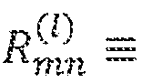 [smc(nn + InwfA) + sinc(n?r - InwfA)] x [sinc(m7i + InwfA) + sincfjrar - InwfA)] (Eq. 5)
The Fourier components of the electric field can be obtained by numerically solving Eq. 4. in practice, for smoothly-varying plasmon modes, only the lowest few Fourier components are needed to accurately approximate the field.
Then, from E(x), the fractional absorbed power in the 2D material is computed as
Ac (w) =

The resonant modes and fractional absorption Α(ω) in the graphene channel are subsequently found by integrating the Joule power density over the graphene ribbon, and normalizing to the incident power of the plane wave (Eq. 6). The absorption spectrum reveals all of the dipole-active plasmon resonances and the relative coupling of these modes to radiation,
FIG. 2C represents the theoretically computed absorption spectrum Α(ω) for several different metal periods Λ, with the graphene channel 22 width w
(w=350 nm) remaining constant. The mobility μ and density n of carriers
(electrons or holes) are n :::: 1 .5x10° cm"'', μ ~ 1000 cmVv-s, respectively. The array shows no discemable plasmon resonance when the period A and the graphene channel width w are comparable, manifesting instead a Drude-like response. However, when the metal contacts (stripes) 18 are made much wider than the graphene chaimeis 22, a strong resonance emerges, characterized by high
absorption in the graphene channels, at a resonant frequency that scales with n w'ifi, similar to the plasmon resonances in uncontacted graphene ribbons, (L. Ju, et a!,, "Graphene plasmonics for tunable terahertz metamaterials", Nature Nanotech. 6, 630-634 (2011); and P. Nene, et ah, "Coupling of plasmon modes in graphene microstructures", Appl. Phys. Lett., 105, 143108 (2014)),
The surrounding material is assumed to be a uniform dielectric, in which case, the maximum achievable absorption in a two-dimensional (metal-graphene grating) is 50% (C, Hi] sum, "Infrared Absorption of Thin Metal Films", J. Opt. Soc. Am 44, 187-191 (1954)),
As shown in FIG. 2C, at the resonant frequency, the graphene absorption reaches a peak of the maximum possible value (50%), even when the geometrical fill factor is only w/A = 1/20 (5%). This suggests (at plasmon frequency) an extremely high confinement of the THz field in the narrow slots 20 where graphene is located. This makes the metal-graphene scheme an attractive candidate for nonlinear THz plasrnonic applications. It was noted that by using known techniques, such as an antireflection coating or a Salisbuiy screen on top of the grating, the thin film limit absorption can be increased to nearly 100%, and a perfect tunable graphene plasrnonic absorber can be achieved.
The calculations confirm that the resonances disappear when the graphene is absent, when the polarization is rotated parallel to the channels, or when the graphene is electrostatically gated to the charge neutral point.
For comparison, in FIG. 2D, an absorption spectrum is shown for the array (FIG, 2B) of electrically isolated graphene channels having the width, carrier density, and mobility identical to that shown in FIG. 2A, which yields a far lower on-resonant absorption (curve a), even when the fill-factor is increased to 50% (curve b).
The nature of the fundamental metal-graphene plasmon resonance is illustrated in FIG. 2E, which shows the charge density calculated at the resonant frequency. For comparison, FIG. 2F shows the charge density profile at plasmon resonance for the uncontacted graphene ribbon (FIG. 2B) of the same dimension.
In the contacted graphene (FIG. 2A), the metal regions act as capacitive reservoir for charge accumulation, and the graphene serves as an inductive channel, thus forming a resonant circuit that interacts strongly with the incident radiation. This phenomena is in contrast to the isolated ribbon case (of FIG. 2B). where the coupling to incident radiation is weaker, and does not depend sensitively on the grating period.
The extension of the spatial mode is accompanied by a significant reduction of plasmon frequency (by about a factor of « 3 ) in comparison with the plasmon frequency in an isolated graphene ribbon.
The factor 3 is an approximate ratio that is consistent with the postulate that a plasma wave incurs an approximate phase shift of approximately π/4 upon
reflection from an open boundary, and 3π/4 upon reflection from a conductive boundary.
The optical properties of the subject metai-graphene plasmonic grating in the siibwavelength limit, when Λ< λ (free space wavelength), can be modeled by an equivalent two-port circuit at the junction of two semi-infinite transmission lines with impedances
 upper and lower regions respectively, as shown in FIG, 3 A, where Z0 = 377Ω , free space impedance.
The graphene behavior can be described by a Drude conductivity (DC)
1 1- ίω/Γ n
iO)LG (Eq. 7) where σ0 = ΙΙβμ. represents the DC sheet conductivity of the graphene layer with carrier concentration n and mobility μ, and Γ≡ eV Jun ih is the scattering rate.
From (Eq. 7), the graphene may be modeled by its ohmic resistance
RG ™ ' Q 1 in series with its kinetic inductance, LQ = (tfn -Q™1 (Yao Yu, et al., "Broad Electrical Tuning of Graphene-Loaded Plasmonic Antennas". Na.no Lett. 13, 1257-1264 (2013)).
RQ and LQ must each be multiplied by a geometrical factor of w/A to account for the filling factor in the subject periodic structure. The conducting
contacts (stripes) 18 act as a capacitive grid (U, Reinhard, "Far-infrared properties of metallic mesh and its complementary structure", infrared Phys, 7, 27-55 (1967); and B, Lewis, et al., "Equivalent-circuit formulas for metal grid reflectors at a dielectric boundary". Appl, Optics, 24, 217-220 (1985)) that can be described by a capacitance CM =
 where€ = {€t + e2)/2 is the average dielectric permittivity.
The finite size graphene channels 22 contribute to an additional parallel capacitance, of CG— 2e0e Aln[sec (7Γνν/2Λ}]/τΓ (Alu Andrea, et al,
"Input Impedance. Nanocircuit Loading, and Radiation Tuning of Optical
Nanoantennas", Phys. Rev. Lett. 101, 043901 (2008)) to result in a total capacitance of C = CM + CG = 2eQe Λ1η[2 csc nw/A)]/n.

The optical response and plasmon resonance of the metal-graphene grating can be approximated from a two-port transmission line model shown in FIGS. 3A - 3B, where FIG. 3A is an equivalent two-port transmission line model
representing the sub-wavelength graphene-metal periodic structure, and FIG. 3B is simplified circuit model where there are no input waves to the system, which is used to determine resonant (plasmon) frequency and damping rate. The
resistance, inductance and capacitances appearing in this model are defined as:
1
σ01 j (Eq. 9)
CG = 2e Aln[sec (nw/2A)]/n (Eq. io)
CM = 2 β Λΐη [esc (nw f 2Α)]/π (Eq. i i) and the incident and substrate regions are modeled as transmission lines with characteristic impedances of Z ≡ respectively.

The graphene and contact capacitances can be combined into a single equivalent capacitance of
C = CM + CG = 2£ Λ1η[2 esc (nw/A)]/n (Eq. 12)
As shown in FIG. 3 A, this circuit models the transmission, reflection, and absoiption for the lowest order plasmon mode in the plasmon device. The plasm on resonance frequency of this circuit is found to be ζ 2 _ e2vF—^ ϊι i ,^q ) υ 2h weQe ln[2 csc(nw/A)] it has been noted that for a fixed duty cycle w/Λ, the resonant frequency in the subject structure scales in proportion to nil w as for the case of
uncontacted graphene ribbons (FIG. 2B). This indicates that the plasmon frequency ¾o can be tuned through the application of a gate voltage Vg or by adjusting the graphene channel width.
The resonant frequency blue-shifts weakly with increasing duty cycle wlA, but in all of the cases, the resonance frequency is lower than that of an uncontacied graphene ribbon of the same width, Eq, 13 shows that increasing the period Λ for a fixed width w will result in a slight red-shift of the plasmon frequency. This is in direct contrast to the case of uncontacied graphene ribbons, where the plasmon frequency is blue-shifted by increasing the period, as a result of the reduced dipolar plasmon mode coupling in adjacent graphene ribbons (P. Nene, et a!,, "Coupling of plasmon modes in graphene microstructures", Appl. Phys, Lett., 105, 143108 (2014)).
The plasmon line width, computed from the equivalent circuit model has been found to be

The first term in Eq, 14 is the conventional Drude line width, which is constrained by the mobility and carrier density, while the second term in Eq. 14 describes the radiative linewidth of the plasmon, which does not depend on the graphene quality or material properties. This second term, which is negligible for uncontacied graphene ribbons (of FIG. 2B) fundamentally limits the quality factor (ξ)=ω</Αω).
 This suggests that increasing Λ improves the quality factor of plasm on resonance, For the parameters considered in FIG, 2A, this equation predicts that for Λ > 10w, and particularly, Λ > 1 1.5-w, a plasmon resonance with Q > 1 can be achieved.
The equivalent circuit model can also be used to predict the condition under which maximum power is delivered to the graphene layer.
TRANSMISSION, REFLECTION AND ABSORPTION
The relationship between the amplitudes of the incoming and outgoing wave amplitudes can be described by a scattering matrix,

For the circuit model shown in FIG. 3 A, the scattering matrix is calculated to be:

where Y:. ~ l/Z, and Υ(ω) is the complex admittance of the combined resistor, capacitor and inductor,
 For waves incident from a region 1, the reflection, transmission and absorption are calculated to be
Υ1~~Υ2 ~~Υ(ω)
(ω) = \S1± (Eq. 19) YtY2
'11 (Eq. 20)
Yi \Υί +Υ2 +Υ(ω) \2
471Κθ{7(ω)}
Α0 (ω) = 1 - β(ω) - (ω) 5q. 21)

RESONANT FREQUENCY AND LINE WIDTH
If there are no input waves applied to the system, the two transmission lines representing regions I and 2 may be simply replaced by their equivalent impedance, which results in the simple second-order circuit shown in FIG. 3B. In this circuit model, the power dissipated i Zj and Z2 represents the radiative loss into regions 1 and 2. respectively, while the power consumed in RG results in absorption in the two-dimensional material. Applying Kirchoff s laws, the voltage v(t) is found to satisfy the following second-order homogenous differential equation:
A/w RG (YI +Y2 ")
v{t) + v(t) + v t) ~ 0 (Eq. 22)
LQ C LQ C LQ j
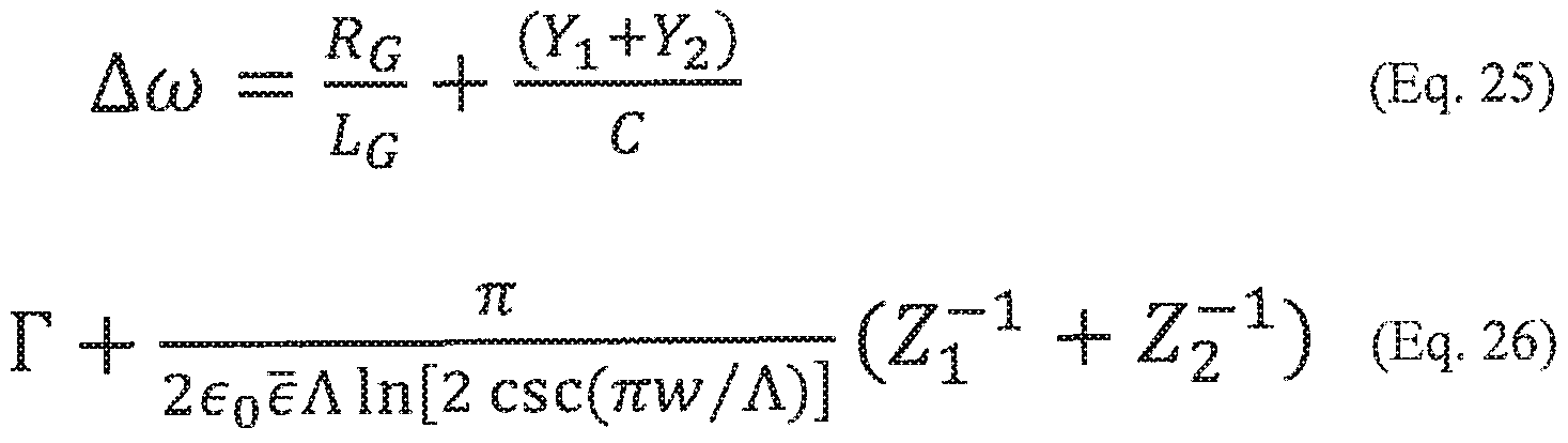
which describes a damped harmonic oscillator. In the limit of low-damping, the resonant frequency (or plasmon frequency) is
o — (Eq. 23)

The damping rate describes the linewidth of the plasmon resonance, which is found to he:
(Eq, 26)
ABSORBED POWER AND IMPEDANCE MATCHING
In many applications it is desired to optimize the power that is absorbed in the graphene layer, by appropriately designing or selecting the properties and dimensions of the metal grating and graphene film. By maximizing the absorption AG (Eq, 21 ) with respect to the complex admittance Υ(ω), the optimal load admittance is found
Yopt = (Y, + Y2)* (Eq. 27)
Since Y> and Y2 are real numbers, (Eq. 27) implies that Υ(ω) must be real, occurs at an optimal frequency that is close to the resonant frequency.
 xrf
xrf
Y i0JoptJ ™" 7™ (Eq. 29) in this case, the condition for maximum power transfer to the graphene layer can be expressed as
RG = Γ - (Y + Y2)/C (Eq. 30) which means that for maximum on-resonant absoφtion5 the intrinsic material damping Γ is equal to the radiation damping.
Under these matched conditions, the lumped circuit may be regarded as impedance matching between two dissimilar media. The maximum fractional absorbed power is
^max = (¾+¾ (Eq' 3 1)
As discussed in previous paragraphs, the maximum on-resonant graphene absorption is achieved when the material scattering rate Γ and radiative decay rates are equal, which is equivalent to an impedance matching between two dissimilar media (Andrea Alu, et al., "Input Impedance, Nanocircuit Loading, and Radiation
Tuning of Optical Nanoantennas", Phys. Rev, Lett., 101, 043901 (2008) and Constantine A. Balanis, "Antenna Theory analysis and design," (2012)).
For the parameters considered in FIG. 2A, this matching condition occurs when A~23w5 which is consistent with FIG. 2C, it is noted that the circuit model can be generalized by including an inductor in series with CM to describe metal- graphene plasmo ic devices coupled to antennas.
In the circuit model, the metal was treated as a perfect conductor. This is a good approximation when metal is gold with Drade conductivity (Γ = 3.33 x ].0! 3 rad/s, 0)P = 1.36 x 10¹⁶ rad/s). It is possible to account for the ohmic loss in the metal by adding a resistor in series with C in the equivalent circuit model.
However, for typical dimensions, frequencies, and conductivities considered herein, the series resistance is calculated to be much smaller than the reactance of the capacitive grid. It is not expected that this equivalent circuit model can be applied at infrared and optical frequencies, where the metallic structure has its own plasmonic behavior which cannot be ignored.
To measure the THz response of metal-contacted plasmons in the subject graphene-based structures, gratings of gold strips 18 have been fabricated on top of epitaxial graphene layer 14 grown on SiC.
An SEM image and side view of the subject device 10 are shown in FIGS. 1 A - IB, respectively. To tune the graphene carrier density, the electrostatic gate voltage Vg has been applied using an electrolytic 24 top gate. The incident beam
32 was polarized perpendicular to the gold stripes 18. The transmission (T) and reflection (R) of the metal-graphene grating devices have been simultaneously measured using conventional FTIR spectroscopy.
FIG. 4A shows the measured transmission as a function of frequency for different canier density levels tuned by application of the gate voltage Vg for a device with Λ = 7μτη and w ~ 350 nm dimensions, A resonant peak was observed in the transmission graph. The piasmonic resonance grows in strength and blue shifts with increasing canier density.
In reflection (FIG. 4B) the plasmon resonance exhibits a minimum which also becomes stronger and blue-shifts by increasing the carrier density. In FIG. 4B, the reflection is presented which is normalized to the lowest carrier density data to exhibit clearer the plasmon resonance dip.
The measured absorption data (A = 1 - R - T) is presented in FIG. 4C, which shows how the frequency and strength of THz resonant absorption can be controlled by tuning the carrier density with a gate voltage Vg. The carrier density was extracted from the plasmon frequency at each gate voltage and by comparing the experimental spectra to finite element calculations.
Finite el ement calculations of the same measured quantities presented in FIGS. 4A, 4B and 4C, respectively, are shown in FIGS. 4D, 4E and 4F. The measurement results and the calculations are seen to be in a satisfactory
agreement.
In the finite element calculations, Fermi-level pinning at graphene-metal junction was ignored. A constant Fermi level across the graphene channel and zero graphene-metal contact resistance were assumed. The close agreement between experimental results and theory suggest that the Fermi-level pinning and non-zero contact resistance effects are negligible in the devices we studied.
However, it is expected that they should have a noticeable effect for narrow graphene channels (<100nm). (P. A. Khomyakov, et al., "Nonlinear screening of charges induced in graphene by metal contacts" Phys. Rev. B82, 1 15437 (2010)). CIRCUIT MODEL VS. FINITE ELEMENT CALCULATIONS
FIGS. 7A - 7D show transmission/reflection for different periods computed by full-wave finite element calculations, and FIGS. 7C - 7D show
transmission/reflection for different periods calculated by the circuit model showed in FIG. 2A, where e\ = 1 (air), e2 =::; 9 (SiC), w = 0.35 μιη, μ = 1000 cmTV-s, n = 1.5 x 1013cm"2.
FIGS. 7 A - 7D compare the transmission (T) and reflection (R) obtained from the full-wave finite element calculation (FIGS. 7A - 7B) with the
approximated values from circuit model (FIGS. 7C - 7D), and a close agreement between the results from circuit model (FIG. 3A) and the exact solution for different grating periods is exhibited.
PLASMON RESONANCE SHIFT (CHANGING w)
FIG. 8 shows the normalized reflection measurement for metal-graphene gratings with two different graphene channel widths (w = 350nm, 200 nm) and for the same carrier density levels. It is seen that the plasrnon resonance has shifted to higher frequencies by about 30% ( id SQnm/'ZQOi i) as expected from the square-root dispersion relation of graphene plasrnon modes.
Similar to the graphene ribbon case with no metal contact (FIG. 2B), plasrnon resonance frequency in metal-graphene structures can also be tuned by changing the graphene channel width (Eq. 14), This was confirmed
experimentally in the subject structure with a narrower graphene channel (w = 200nm). This data demonstrates that plasmonic resonance can be produced in metal contacted graphene and that they can be tuned and result in strongly
enhanced absorption at a selected resonant frequency. These observations show that metal-contacted graphene has great potential for THz optoelectronics, and the tunable hybrid plasmonic modes can be incorporated in graphene-integrated metamaterials, where the metal-graphene plasrnon enhances the metamaterial resonance.
It is noted that the metal-graphene plasmonic structure can exhibit near 100% resonant transmission in a high mobility graphene sample, a feature that is useful in THz transmission filters or modulators.
The charges of the transmission of the plasmonic device have been investigated by increasing the graphene mobility. FIG. 5A shows the calculated power transmission spectrum T(j) for a case of /Λ = 1/20, and for graphene mobilities ranging from 1000 to 100,000 cm 7V-S in = 1.5 x 10" cm"'). The mobility μ of carriers in graphene may be 1000 cm2 V-s for carrier density n=T,5 x 10° cm"". When the graphene mobility is increased, the graphene absorption decreases, but is replaced by a resonant peak in the transmission that approaches 100% transmission in the limit of high mobility. Again, it is noted that this resonance shifts to zero frequency (low-pass filter response) when the graphene is absent or charge-neutral, showing that the inductive graphene channel is important to support the plasmonic resonance.
As shown in FIG. 5B, the spectral width of this resonance decreases inversely with the mobility, but reaches a plateau in the limit of high mobility. Above this point, the plasmon linewidth is dominated by radiation damping, and cannot be further reduced by improving the material quality (Eq. 14). In contrast to isolated graphene ribbons (shown in FIG. 2B), the plasmons in metal-contacted graphene are naturally radiative, a feature that can have important consequences in tunable graphene emitters or sensors.
FIG. 5C demonstrates the tunability of the near 100% resonant transmission through changing the graphene carrier density. These results show metal-
graphene grating plasmonic device on a high mobility graphene sample is an attractive candidate for tunable THz modulators, or a bandpass filters,
FIG, 5D plots the calculated absorption AG(f) in the structure with
Λ=2.8μηι under study for six different graphene mobilities ranging from 2,000 to 20,000 cm2/V-s. The absorption at the 3rd order peak approaches the theoretical maximum (50%) for graphene mobility of 9,000 cm2/V-s. This demonstrates that, unlike most plasmonic structures in which higher order modes are weakly coupled to the incident plane-wave, the plasmon modes in the hybrid graphene-metal system can be efficiently excited by appropriately choosing the geometry of the metal contacts and graphene properties.
FIGS. 9A - 9B illustrate the sequence of manufacturing steps for fabrication of the subject of the electronic structure 10. As shown in FIG. 9 A, a single layer of graphene 14 was formed on the substrate 12 using the Si sublimation process in an Ar (Argon) ambient. The starting substrate 12 was an 8 mm x 8 mm semi-insulating 6H-S1C (0001) wafer (resistivity >10i0 Ω-cm) that was misoriented from the basal plane by proximity 0.1°. The substrate chip was etched in ¾ prior to graphene synthesis.
As shown in FIG. 9B5 a layer of PMMA photoresist was formed on the graphene layer and patterned using electronic beam lithography (FIG. 9C) followed by Cr/Au (having the thickness of 5nm/75nm, respectively) thermal
evaporation (as shown in FIG. 9D). Cr was used as the adhesion layer for the enhanced adhering of Au to graphene.
A lift-off process was subsequently performed to remove the residues of PMMA, as shown in FIG. 9E, to form an array of gold strips 18 on the graphene layer 14.
The Au strips 18 were produced 1.5 mm long, and the entire metal grating had the width of 1.5 mm, thus forming the metal grating with an area of approximately 2.25 mm .
To electrically isolate the metal grating from other parts of the
graphene/SiC chip, a narrow ribbon (7μηι) was defined by electron-beam lithography using PMMA photoresist as a mask, and oxygen plasma process was conducted to remove the masked areas.
Finally, as shown in FIG. 9F5 electrolyte (for example polyethylene oxide/LiClQ4) was drop-cast on the sample as a top gate. The gate voltage was applied between the grating of the device 10 and the electrically isolated part of the SiC graphene substrate.
Far infrared simultaneous transmission/reflection measurements were performed in a Bomem DA- 8 FTIR system with a mercury lamp as a source and tvvo 4K silicon composite bolometers as detectors. A polarizer was placed in the
beam path to pass only polarization perpendicular to the metal strips. The 1.5 x
1.5 mm square metal -graph ene grating device was mounted on a copper plate with a 1.5 mm diameter aperture. The incident THz beam illuminated the back of the device making an angle about 10° from the normal incidence. One bolometer was located on the transmitted beam path, and another bolometer is located at the reflection side of the experimental setup.
Frequency-domain finite element calculations were performed on the unit cell (shown in FIG. 6) of the metal-graphene grating formed on the top of the SiC substrate (having the refracting index of ~3) with periodic boundary condition. Gold was modeled as a 75 nm thick Drude metal with Γ = 3.33 x 10iJ rad/s, ωρ :::: 1 .36 x 1016 rad/s. The electrolyte on the top of the metal grating was modeled as dielectric (refractive index = 1.7).
Currents, fields and charge density in graphene and metal were calculated. Transmission and reflection of an incident plane-wave, polarized perpendicular to the metal strips, were also calculated. In the carrier density dependent
calculations, a constant scattering rate was assumed for graphene. Mobility was taken to be 1010 cm2/V-s at the carriers density n= 5 x 10i2 cm"2, based on van der Pauw.Hall measurements taken on the full graphene layer on SiC sample prior to the processing.
In the finite element calculations, Fermi-level pinning at graphene-metal junction was ignored. A constant Fermi level across the graphene channel and zero graphene-metal contact resistance were assumed. The close agreement between experimental results and theoretical calculations suggest that the Fermi- level pinning and non-zero contact resistance effects are negligible in the devices under study. However, it is expected that they should have a noticeable effect for narrow graphene channels (<100 nm.).
Although this invention has been described in connection with specific forms and embodiments thereof, it will be appreciated that various modifications other than those discussed above may be resorted to without departing from the spirit or scope of the invention as defined in the appended claims. For example, functionally equivalent elements may be substituted for those specifically shown and described, certain features may be used independently of other features, and in certain cases, particular locations of the elements may be reversed or interposed, all without departing from the spirit or scope of the invention as defined in the appended claims.
Claims
1. A plasmon-enhanced terahertz graphene-based optoelectronic structure, comprising:
a substrate,
a conductive layer formed above said substrate,
at least one plasmonic graphene channel embedded in said conductive layer, and
a source of an electromagnetic wave of a predetermined wavelength, wherein said electromagnetic wave is incident on said at least one plasmonic graphene channel and is polarized substantially perpendicular thereto,
wherein said at least one plasmonic graphene channel has a width smaller than said predetermined wavelength of the electromagnetic wave and is tunable to produce a controllable plasmon-enhanced resonance signal,
2. The plasmon-enhanced terahertz graphene-based optoelectronic structure of Claim 1, further including:
a first periodic array of conductive stripes formed in said conductive layer above said substrate, said conductive stripes extending in a spaced apart relationship each with respect to the other with a gap defined between adjacent conductive stripes, and
a layer of graphene sandwiched between said substrate and said first periodic array of said conductive stripes, said layer of graphene comprising a second periodic array of said at least one plasmonic graphene channels, each confined in a respective gap between said adjacent conductive stripes, wherein a width of each of said conductive stripes exceeds the width of said at least one plasmonic graphene channel.
3. The plasmon-enhanced terahertz graphene-based optoelectronic structure of Claim 2, further including an electrolyte layer positioned atop and enveloping said first periodic array of conductive stripes and said second periodic array of said plasmonic graphene channels.
4. The plasmon-enhanced terahertz graphene-based optoelectronic structure of Claim 3, further including a gate terminal coupled to said electrolyte layer, and
a source of a gate voltage Vg applied between said gate terminal and said graphene layer.
5. The plasmon-enhanced terahertz graphene-based optoelectronic structure of Claim 4. wherein upon application of said gate voltage of a predetermined value VgJ said polarized electromagnetic wave excites transverse
plasmon resonance in said at least one plasmonic graphene channel, thereby producing a plasmon-enhanced resonance at a plasmon resonance frequency.
6. The plasmon-enhanced terahertz graphene-based optoelectronic structure of Claim 5, wherein plasmon resonance frequency and strength of the resonance absorption is controlled by controlling said gate voltage Vg to tune carriers density in said at least one plasmonic graphene layer.
7, The plasmon-enhanced terahertz graphene-based optoelectronic structure of Claim 5, wherein said plasmon resonance frequency and strength of the resonance absorption is controlled by adjusting the width of said conductive stripes,
8. The plasmon-enhanced terahertz graphene-based optoelectronic structure of Claim 5, wherein said plasmon resonance frequency and strength of the resonance absorption is controlled by adjusting the width of said at least one plasmonic graphene channel
9, The plasmon-enhanced terahertz graphene-based optoelectronic structure of Claim 2, wherein the width of said at least one plasmonic graphene channel is in a sub-micron range.
10. The plasmon-enhanced terahertz graphene based optoelectronic structure of Claim 2, wherein the width of said at least one graphene channel ranges from 100 run to few micrometers.
1 1. The plasmon-enhanced terahertz graphene-based optoelectronic structure of Claim 1, wherein said substrate is fabricated from SiC (0001) material.
12. The plasmon-enhanced terahertz graphene-based optoelectronic structure of Claim 2, wherein said plasrnonic graphene channels in said second periodic array thereof extend substantially in parallel each to the other.
13. The plasmon-enhanced terahertz graphene-based optoelectronic structure of Claim 2, wherein a ratio AJw between the width w of said at least one plasrnonic graphene channel and a period Λ of said first array of conductive stripes exceeds 10.
14. The plasmon-enhanced terahertz graphene-based optoelectronic structure of Claim 13, wherein said ratio is within the approximate range of 20 to 23.
15. The plasmon-enhanced terahertz graphene-based optoelectronic structure of Claim 13, wherein said period Λ of said first array of conductive stripes ranges between 1 m to 9 μηι.
16. The plasmon-enhanced terahertz graphene-based optoelectronic structure of Claim 6, wherein a ratio A/w of a period Λ of said first array of conductive stripes to the width w of said at least one plasmonic graphene channel is approximately 20: 1, wherein the mobility μ of carriers in said at least one plasmonic graphene channel is approximately 1.000 cmVv-s, and the carrier density n in said at least one plasmonic graphene layer is approximately 1.5 x 1013cm~2.
17. The plasmon-enhanced terahertz graphene-based optoelectronic structure of Claim 6, wherein said mobility μ of carriers in said at least one plasmonic graphene layer is approximately 50,000 cm /V-s or higher.
18 The plasmon-enhanced terahertz graphene-based optoelectronic structure of Claim 2. wherein said conductive stripes are made from at least one metal.
19, A method of fabrication of a plasmon-enhanced terahertz graphene- based optoelectronic structure comprising:
(a) epitaxially forming a single layer of graphene on a SiC substrate, and
(b) forming, on said single layer of graphene, a first periodic array of metallic stripes extending substantially in paralleled relationship one with respect to another with respective gaps defined between neighboring metallic stripes, wherein a second periodic array of graphene channels is sandwiched between said substrate and said first periodic array of metallic stripes, said second periodic array including a plurality of graphene channels defined by areas of said single layer of graphene confined in respective gaps between neighboring metallic stripes,
(c) applying a layer of electrolyte atop of said first periodic array of metallic stripes to envelope and being in contact with said first array of metallic stripes and said second array of graphene channels,
(d) connecting a gate terminal to said electrolyte layer, and
(e) coupling a source of gate voltage between said gate terminal and said graphene layer,
wherein a ratio of a period Λ of said first periodic array to a width w of each said graphene channel exceeds 10, wherein the width w of said each graphene channel is in sub-micron range, and wherein the mobility μ of carriers in said graphene layer ranges from 1000 to 100,000 cm2/V-s.
20. The method of Claim 19, further comprising:
exposing said optoelectronic structure to an incident light polarized in a direction perpendicular to elements selected from a group consisting of said graphene channels and said metallic stripes, to excite transverse plasmon resonance in graphene, and
controlling said gate voltage to tune carrier density of said graphene layer, to obtaining a plasmon resonance response.
Priority Applications (1)
| Application Number | Priority Date | Filing Date | Title |
|---|---|---|---|
| US15/735,662 US10672933B2 (en) | 2015-06-15 | 2016-06-14 | Hybrid metal-graphene terahertz optoelectronic system with tunable plasmonic resonance and method of fabrication |
Applications Claiming Priority (2)
| Application Number | Priority Date | Filing Date | Title |
|---|---|---|---|
| US201562175695P | 2015-06-15 | 2015-06-15 | |
| US62/175,695 | 2015-06-15 |
Publications (2)
| Publication Number | Publication Date |
|---|---|
| WO2016209666A2 true WO2016209666A2 (en) | 2016-12-29 |
| WO2016209666A3 WO2016209666A3 (en) | 2017-02-02 |
Family
ID=57585393
Family Applications (1)
| Application Number | Title | Priority Date | Filing Date |
|---|---|---|---|
| PCT/US2016/037393 Ceased WO2016209666A2 (en) | 2015-06-15 | 2016-06-14 | Hybrid metal-graphene terahertz optoelectronic system with tunable plasmonic resonance and method of fabrication |
Country Status (2)
| Country | Link |
|---|---|
| US (1) | US10672933B2 (en) |
| WO (1) | WO2016209666A2 (en) |
Cited By (11)
| Publication number | Priority date | Publication date | Assignee | Title |
|---|---|---|---|---|
| CN108110433A (en) * | 2017-11-22 | 2018-06-01 | 桂林电子科技大学 | Surpass the multi-functional THz polarization converters on surface based on graphene-metal mixed |
| CN108793057A (en) * | 2018-07-06 | 2018-11-13 | 江苏心磁超导体有限公司 | Silicon carbide-based graphene superconduction TES devices and preparation method thereof |
| CN108899413A (en) * | 2018-07-06 | 2018-11-27 | 江苏心磁超导体有限公司 | Graphene TES superconductive device and preparation method thereof |
| CN109164067A (en) * | 2018-09-04 | 2019-01-08 | 华南师范大学 | A kind of graphene binary cycle grating sensor for infrared band |
| WO2019136542A1 (en) * | 2018-01-11 | 2019-07-18 | Universidade Federal Do Pará | Controllable w-shaped three-port graphene-based circulator in the thz band |
| CN110515224A (en) * | 2019-09-04 | 2019-11-29 | 哈尔滨理工大学 | A dual-band flexible and selectively tunable graphene-metal groove metamaterial terahertz slow-light device |
| CN111710749A (en) * | 2020-04-23 | 2020-09-25 | 中国科学院上海技术物理研究所 | Splicing structure and realization method of long line detector based on multi-substrate secondary splicing |
| CN111883888A (en) * | 2020-08-07 | 2020-11-03 | 安徽华东光电技术研究所有限公司 | W-band reconfigurable microstrip filter based on intercalated graphene and manufacturing method thereof |
| CN113328259A (en) * | 2021-07-05 | 2021-08-31 | 江苏大学 | Metamaterial absorber, device and system and preparation method thereof |
| CN113488777A (en) * | 2021-06-10 | 2021-10-08 | 上海交通大学 | Graphene patch type terahertz Fabry-Perot resonant antenna and implementation method thereof |
| CN113675618A (en) * | 2021-08-19 | 2021-11-19 | 太原理工大学 | Ultra-wideband terahertz absorption material with double truncated pyramid structure and absorber |
Families Citing this family (20)
| Publication number | Priority date | Publication date | Assignee | Title |
|---|---|---|---|---|
| WO2017119978A2 (en) * | 2015-12-07 | 2017-07-13 | Georgetown University | Epitaxial graphene quantum dots for high-performance terahertz bolometers |
| CN109494293B (en) * | 2018-12-28 | 2024-09-13 | 同方威视技术股份有限公司 | Terahertz detector and method for manufacturing the same |
| US12464834B2 (en) | 2019-04-29 | 2025-11-04 | Rensselaer Polytechnic Institute | Terahertz and sub-terahertz devices |
| CN110473957B (en) * | 2019-09-04 | 2023-04-07 | 哈尔滨理工大学 | Terahertz ring dipole metamaterial device capable of being dynamically regulated and controlled based on selective electrostatic doping of graphene and preparation method thereof |
| CN110954496B (en) | 2019-11-15 | 2021-01-08 | 浙江大学 | Sample signal amplification method using terahertz waveband graphene absorber |
| CN112014350B (en) * | 2020-08-13 | 2022-08-26 | 中国计量大学 | Reflective terahertz refractive index adjustable sensor |
| US12300884B2 (en) * | 2021-04-26 | 2025-05-13 | University Of Florida Research Foundation, Inc. | Parallelly and diagonally placed meander-line slot resonators for mutual coupling reduction |
| US12107331B2 (en) * | 2021-05-30 | 2024-10-01 | Government Of The United States As Represented By The Secretary Of The Air Force | Smart metal-graphene hybrid reflectarray at THz frequencies |
| CN113471327B (en) * | 2021-06-22 | 2022-08-02 | 中国科学院重庆绿色智能技术研究院 | High-gain graphene photoelectric detector based on double-gate voltage regulation and control and preparation method thereof |
| CN113670848B (en) * | 2021-08-23 | 2022-08-02 | 中国人民解放军军事科学院国防科技创新研究院 | High-resolution broadband terahertz detector based on pixelized structure and detection method |
| CN113948871B (en) * | 2021-09-28 | 2023-05-02 | 西安交通大学 | Frequency-adjustable terahertz electromagnetic induction transparent device, frequency regulation method and application thereof |
| CN113917581B (en) * | 2021-10-09 | 2024-08-16 | 青岛大学 | Terahertz near-perfect absorber with chiral selection |
| CN114094345B (en) * | 2021-11-22 | 2024-10-15 | 郑州大学 | Thermal control multi-band indium antimonide perfect wave absorber and application thereof |
| CN113948876B (en) * | 2021-11-22 | 2024-10-15 | 郑州大学 | A demetallized dynamically thermally tunable triple narrow-band terahertz perfect absorber |
| CN114038927B (en) * | 2021-12-01 | 2023-12-29 | 电子科技大学 | Ferroelectric integrated graphene plasma terahertz detector with high response |
| CN114421169B (en) * | 2021-12-10 | 2024-11-15 | 北京邮电大学 | Antenna device and terahertz dual-frequency polarization metasurface unit |
| CN115764327B (en) * | 2022-11-21 | 2026-02-17 | 南京航空航天大学 | Broadband terahertz wave absorber based on borane and strain regulation thereof and design method thereof |
| CN116230286B (en) * | 2023-01-09 | 2026-04-10 | 无锡学院 | A graphene metasurface structure for particle transport and sorting and its applications |
| CN116154484B (en) * | 2023-04-04 | 2023-07-04 | 湖南工商大学 | Binary channels terahertz is absorption device entirely now |
| CN120594439B (en) * | 2025-07-22 | 2026-03-13 | 延安大学 | A microcavity-based terahertz mercury ion detection device and its usage method |
Family Cites Families (3)
| Publication number | Priority date | Publication date | Assignee | Title |
|---|---|---|---|---|
| JP6161554B2 (en) * | 2013-04-26 | 2017-07-12 | 三菱電機株式会社 | Electromagnetic wave detector and electromagnetic wave detector array |
| US9105791B1 (en) * | 2013-09-16 | 2015-08-11 | Sandia Corporation | Tunable plasmonic crystal |
| WO2016140946A1 (en) | 2015-03-02 | 2016-09-09 | University Of Maryland, College Park | Plasmon-enhanced terahertz graphene-based photodetector and method of fabrication |
-
2016
- 2016-06-14 US US15/735,662 patent/US10672933B2/en active Active
- 2016-06-14 WO PCT/US2016/037393 patent/WO2016209666A2/en not_active Ceased
Cited By (15)
| Publication number | Priority date | Publication date | Assignee | Title |
|---|---|---|---|---|
| CN108110433A (en) * | 2017-11-22 | 2018-06-01 | 桂林电子科技大学 | Surpass the multi-functional THz polarization converters on surface based on graphene-metal mixed |
| CN108110433B (en) * | 2017-11-22 | 2024-04-12 | 桂林电子科技大学 | Multifunctional THz polarization converter based on graphene-metal mixed super surface |
| WO2019136542A1 (en) * | 2018-01-11 | 2019-07-18 | Universidade Federal Do Pará | Controllable w-shaped three-port graphene-based circulator in the thz band |
| CN108793057A (en) * | 2018-07-06 | 2018-11-13 | 江苏心磁超导体有限公司 | Silicon carbide-based graphene superconduction TES devices and preparation method thereof |
| CN108899413A (en) * | 2018-07-06 | 2018-11-27 | 江苏心磁超导体有限公司 | Graphene TES superconductive device and preparation method thereof |
| CN109164067A (en) * | 2018-09-04 | 2019-01-08 | 华南师范大学 | A kind of graphene binary cycle grating sensor for infrared band |
| CN109164067B (en) * | 2018-09-04 | 2024-07-16 | 华南师范大学 | Graphene bi-periodic grating sensor for infrared band |
| CN110515224B (en) * | 2019-09-04 | 2022-11-08 | 哈尔滨理工大学 | A dual-band flexible and selectively tunable graphene-metal groove metamaterial terahertz slow-light device |
| CN110515224A (en) * | 2019-09-04 | 2019-11-29 | 哈尔滨理工大学 | A dual-band flexible and selectively tunable graphene-metal groove metamaterial terahertz slow-light device |
| CN111710749A (en) * | 2020-04-23 | 2020-09-25 | 中国科学院上海技术物理研究所 | Splicing structure and realization method of long line detector based on multi-substrate secondary splicing |
| CN111883888A (en) * | 2020-08-07 | 2020-11-03 | 安徽华东光电技术研究所有限公司 | W-band reconfigurable microstrip filter based on intercalated graphene and manufacturing method thereof |
| CN113488777A (en) * | 2021-06-10 | 2021-10-08 | 上海交通大学 | Graphene patch type terahertz Fabry-Perot resonant antenna and implementation method thereof |
| CN113328259A (en) * | 2021-07-05 | 2021-08-31 | 江苏大学 | Metamaterial absorber, device and system and preparation method thereof |
| CN113675618A (en) * | 2021-08-19 | 2021-11-19 | 太原理工大学 | Ultra-wideband terahertz absorption material with double truncated pyramid structure and absorber |
| CN113675618B (en) * | 2021-08-19 | 2023-11-14 | 太原理工大学 | Ultra-broadband terahertz absorbing materials and absorbers with double truncated pyramid structures |
Also Published As
| Publication number | Publication date |
|---|---|
| US20180315880A1 (en) | 2018-11-01 |
| WO2016209666A3 (en) | 2017-02-02 |
| US10672933B2 (en) | 2020-06-02 |
Similar Documents
| Publication | Publication Date | Title |
|---|---|---|
| US10672933B2 (en) | Hybrid metal-graphene terahertz optoelectronic system with tunable plasmonic resonance and method of fabrication | |
| Rouhi et al. | Terahertz graphene optics | |
| Jadidi et al. | Tunable terahertz hybrid metal–graphene plasmons | |
| Rahm et al. | THz wave modulators: a brief review on different modulation techniques | |
| Badri et al. | Narrowband-to-broadband switchable and polarization-insensitive terahertz metasurface absorber enabled by phase-change material | |
| Kakenov et al. | Observation of gate-tunable coherent perfect absorption of terahertz radiation in graphene | |
| Xia et al. | The interaction of light and graphene: basics, devices, and applications | |
| Yao et al. | Wide wavelength tuning of optical antennas on graphene with nanosecond response time | |
| US10084102B2 (en) | Plasmon-enhanced terahertz graphene-based photodetector and method of fabrication | |
| Forouzmand et al. | Tunable two dimensional optical beam steering with reconfigurable indium tin oxide plasmonic reflectarray metasurface | |
| Xing et al. | A dual-band THz absorber based on graphene sheet and ribbons | |
| Wang et al. | Toward ultimate control of terahertz wave absorption in graphene | |
| US7847254B2 (en) | Photoconductive device | |
| Lee et al. | Broadband modulation of terahertz waves with non-resonant graphene meta-devices | |
| De Nicola et al. | Graphene plasmonic fractal metamaterials for broadband photodetectors | |
| Kumar et al. | Thermally-electrically tunable broadband ultrathin metal-free THz absorber | |
| Arezoomandan et al. | Tunable terahertz metamaterials employing layered 2-D materials beyond graphene | |
| Dutta-Gupta et al. | Electrical tuning of the polarization state of light using graphene-integrated anisotropic metasurfaces | |
| Min et al. | A novel dual-band terahertz metamaterial modulator | |
| Mylnikov et al. | Limiting capabilities of two-dimensional plasmonics in electromagnetic wave detection | |
| Mencarelli et al. | Design of a coplanar graphene-based nano-patch antenna for microwave application | |
| Ghirardini et al. | Tunable broadband light emission from graphene | |
| Li et al. | High-speed efficient on-chip electro-optic modulator based on midinfrared hyperbolic metamaterials | |
| Suess et al. | Role of transient reflection in graphene nonlinear infrared optics | |
| Ullah et al. | Electrically enhanced graphene-metal plasmonic antenna for infrared sensing |
Legal Events
| Date | Code | Title | Description |
|---|---|---|---|
| 121 | Ep: the epo has been informed by wipo that ep was designated in this application |
Ref document number: 16815060 Country of ref document: EP Kind code of ref document: A2 |
|
| NENP | Non-entry into the national phase |
Ref country code: DE |
|
| 122 | Ep: pct application non-entry in european phase |
Ref document number: 16815060 Country of ref document: EP Kind code of ref document: A2 |