WO2016208704A1 - 半導体デバイス電極用のシリサイド合金膜及びシリサイド合金膜の製造方法 - Google Patents
半導体デバイス電極用のシリサイド合金膜及びシリサイド合金膜の製造方法 Download PDFInfo
- Publication number
- WO2016208704A1 WO2016208704A1 PCT/JP2016/068768 JP2016068768W WO2016208704A1 WO 2016208704 A1 WO2016208704 A1 WO 2016208704A1 JP 2016068768 W JP2016068768 W JP 2016068768W WO 2016208704 A1 WO2016208704 A1 WO 2016208704A1
- Authority
- WO
- WIPO (PCT)
- Prior art keywords
- silicide
- metal
- alloy film
- silicide alloy
- film
- Prior art date
- Legal status (The legal status is an assumption and is not a legal conclusion. Google has not performed a legal analysis and makes no representation as to the accuracy of the status listed.)
- Ceased
Links
Images





Classifications
-
- H—ELECTRICITY
- H10—SEMICONDUCTOR DEVICES; ELECTRIC SOLID-STATE DEVICES NOT OTHERWISE PROVIDED FOR
- H10D—INORGANIC ELECTRIC SEMICONDUCTOR DEVICES
- H10D64/00—Electrodes of devices having potential barriers
- H10D64/01—Manufacture or treatment
- H10D64/013—Manufacture or treatment of electrodes having a conductor capacitively coupled to a semiconductor by an insulator
- H10D64/01302—Manufacture or treatment of electrodes having a conductor capacitively coupled to a semiconductor by an insulator the insulator being formed after the semiconductor body, the semiconductor being silicon
- H10D64/01304—Manufacture or treatment of electrodes having a conductor capacitively coupled to a semiconductor by an insulator the insulator being formed after the semiconductor body, the semiconductor being silicon characterised by the conductor
- H10D64/01306—Manufacture or treatment of electrodes having a conductor capacitively coupled to a semiconductor by an insulator the insulator being formed after the semiconductor body, the semiconductor being silicon characterised by the conductor the conductor comprising a layer of silicon contacting the insulator, e.g. polysilicon
- H10D64/01308—Manufacture or treatment of electrodes having a conductor capacitively coupled to a semiconductor by an insulator the insulator being formed after the semiconductor body, the semiconductor being silicon characterised by the conductor the conductor comprising a layer of silicon contacting the insulator, e.g. polysilicon the conductor further comprising a non-elemental silicon additional conductive layer, e.g. a metal silicide layer formed by the reaction of silicon with an implanted metal
- H10D64/0131—Manufacture or treatment of electrodes having a conductor capacitively coupled to a semiconductor by an insulator the insulator being formed after the semiconductor body, the semiconductor being silicon characterised by the conductor the conductor comprising a layer of silicon contacting the insulator, e.g. polysilicon the conductor further comprising a non-elemental silicon additional conductive layer, e.g. a metal silicide layer formed by the reaction of silicon with an implanted metal the additional conductive layer comprising a silicide layer formed by the silicidation reaction between the layer of silicon with a metal layer which is not formed by metal implantation
-
- C—CHEMISTRY; METALLURGY
- C23—COATING METALLIC MATERIAL; COATING MATERIAL WITH METALLIC MATERIAL; CHEMICAL SURFACE TREATMENT; DIFFUSION TREATMENT OF METALLIC MATERIAL; COATING BY VACUUM EVAPORATION, BY SPUTTERING, BY ION IMPLANTATION OR BY CHEMICAL VAPOUR DEPOSITION, IN GENERAL; INHIBITING CORROSION OF METALLIC MATERIAL OR INCRUSTATION IN GENERAL
- C23C—COATING METALLIC MATERIAL; COATING MATERIAL WITH METALLIC MATERIAL; SURFACE TREATMENT OF METALLIC MATERIAL BY DIFFUSION INTO THE SURFACE, BY CHEMICAL CONVERSION OR SUBSTITUTION; COATING BY VACUUM EVAPORATION, BY SPUTTERING, BY ION IMPLANTATION OR BY CHEMICAL VAPOUR DEPOSITION, IN GENERAL
- C23C14/00—Coating by vacuum evaporation, by sputtering or by ion implantation of the coating forming material
- C23C14/58—After-treatment
- C23C14/5806—Thermal treatment
-
- C—CHEMISTRY; METALLURGY
- C22—METALLURGY; FERROUS OR NON-FERROUS ALLOYS; TREATMENT OF ALLOYS OR NON-FERROUS METALS
- C22C—ALLOYS
- C22C27/00—Alloys based on rhenium or a refractory metal not mentioned in groups C22C14/00 or C22C16/00
-
- C—CHEMISTRY; METALLURGY
- C22—METALLURGY; FERROUS OR NON-FERROUS ALLOYS; TREATMENT OF ALLOYS OR NON-FERROUS METALS
- C22C—ALLOYS
- C22C28/00—Alloys based on a metal not provided for in groups C22C5/00 - C22C27/00
-
- C—CHEMISTRY; METALLURGY
- C22—METALLURGY; FERROUS OR NON-FERROUS ALLOYS; TREATMENT OF ALLOYS OR NON-FERROUS METALS
- C22C—ALLOYS
- C22C30/00—Alloys containing less than 50% by weight of each constituent
-
- C—CHEMISTRY; METALLURGY
- C23—COATING METALLIC MATERIAL; COATING MATERIAL WITH METALLIC MATERIAL; CHEMICAL SURFACE TREATMENT; DIFFUSION TREATMENT OF METALLIC MATERIAL; COATING BY VACUUM EVAPORATION, BY SPUTTERING, BY ION IMPLANTATION OR BY CHEMICAL VAPOUR DEPOSITION, IN GENERAL; INHIBITING CORROSION OF METALLIC MATERIAL OR INCRUSTATION IN GENERAL
- C23C—COATING METALLIC MATERIAL; COATING MATERIAL WITH METALLIC MATERIAL; SURFACE TREATMENT OF METALLIC MATERIAL BY DIFFUSION INTO THE SURFACE, BY CHEMICAL CONVERSION OR SUBSTITUTION; COATING BY VACUUM EVAPORATION, BY SPUTTERING, BY ION IMPLANTATION OR BY CHEMICAL VAPOUR DEPOSITION, IN GENERAL
- C23C14/00—Coating by vacuum evaporation, by sputtering or by ion implantation of the coating forming material
- C23C14/06—Coating by vacuum evaporation, by sputtering or by ion implantation of the coating forming material characterised by the coating material
- C23C14/14—Metallic material, boron or silicon
-
- C—CHEMISTRY; METALLURGY
- C23—COATING METALLIC MATERIAL; COATING MATERIAL WITH METALLIC MATERIAL; CHEMICAL SURFACE TREATMENT; DIFFUSION TREATMENT OF METALLIC MATERIAL; COATING BY VACUUM EVAPORATION, BY SPUTTERING, BY ION IMPLANTATION OR BY CHEMICAL VAPOUR DEPOSITION, IN GENERAL; INHIBITING CORROSION OF METALLIC MATERIAL OR INCRUSTATION IN GENERAL
- C23C—COATING METALLIC MATERIAL; COATING MATERIAL WITH METALLIC MATERIAL; SURFACE TREATMENT OF METALLIC MATERIAL BY DIFFUSION INTO THE SURFACE, BY CHEMICAL CONVERSION OR SUBSTITUTION; COATING BY VACUUM EVAPORATION, BY SPUTTERING, BY ION IMPLANTATION OR BY CHEMICAL VAPOUR DEPOSITION, IN GENERAL
- C23C14/00—Coating by vacuum evaporation, by sputtering or by ion implantation of the coating forming material
- C23C14/06—Coating by vacuum evaporation, by sputtering or by ion implantation of the coating forming material characterised by the coating material
- C23C14/14—Metallic material, boron or silicon
- C23C14/16—Metallic material, boron or silicon on metallic substrates or on substrates of boron or silicon
-
- C—CHEMISTRY; METALLURGY
- C23—COATING METALLIC MATERIAL; COATING MATERIAL WITH METALLIC MATERIAL; CHEMICAL SURFACE TREATMENT; DIFFUSION TREATMENT OF METALLIC MATERIAL; COATING BY VACUUM EVAPORATION, BY SPUTTERING, BY ION IMPLANTATION OR BY CHEMICAL VAPOUR DEPOSITION, IN GENERAL; INHIBITING CORROSION OF METALLIC MATERIAL OR INCRUSTATION IN GENERAL
- C23C—COATING METALLIC MATERIAL; COATING MATERIAL WITH METALLIC MATERIAL; SURFACE TREATMENT OF METALLIC MATERIAL BY DIFFUSION INTO THE SURFACE, BY CHEMICAL CONVERSION OR SUBSTITUTION; COATING BY VACUUM EVAPORATION, BY SPUTTERING, BY ION IMPLANTATION OR BY CHEMICAL VAPOUR DEPOSITION, IN GENERAL
- C23C14/00—Coating by vacuum evaporation, by sputtering or by ion implantation of the coating forming material
- C23C14/06—Coating by vacuum evaporation, by sputtering or by ion implantation of the coating forming material characterised by the coating material
- C23C14/14—Metallic material, boron or silicon
- C23C14/16—Metallic material, boron or silicon on metallic substrates or on substrates of boron or silicon
- C23C14/165—Metallic material, boron or silicon on metallic substrates or on substrates of boron or silicon by cathodic sputtering
-
- C—CHEMISTRY; METALLURGY
- C23—COATING METALLIC MATERIAL; COATING MATERIAL WITH METALLIC MATERIAL; CHEMICAL SURFACE TREATMENT; DIFFUSION TREATMENT OF METALLIC MATERIAL; COATING BY VACUUM EVAPORATION, BY SPUTTERING, BY ION IMPLANTATION OR BY CHEMICAL VAPOUR DEPOSITION, IN GENERAL; INHIBITING CORROSION OF METALLIC MATERIAL OR INCRUSTATION IN GENERAL
- C23C—COATING METALLIC MATERIAL; COATING MATERIAL WITH METALLIC MATERIAL; SURFACE TREATMENT OF METALLIC MATERIAL BY DIFFUSION INTO THE SURFACE, BY CHEMICAL CONVERSION OR SUBSTITUTION; COATING BY VACUUM EVAPORATION, BY SPUTTERING, BY ION IMPLANTATION OR BY CHEMICAL VAPOUR DEPOSITION, IN GENERAL
- C23C14/00—Coating by vacuum evaporation, by sputtering or by ion implantation of the coating forming material
- C23C14/06—Coating by vacuum evaporation, by sputtering or by ion implantation of the coating forming material characterised by the coating material
- C23C14/14—Metallic material, boron or silicon
- C23C14/18—Metallic material, boron or silicon on other inorganic substrates
-
- C—CHEMISTRY; METALLURGY
- C23—COATING METALLIC MATERIAL; COATING MATERIAL WITH METALLIC MATERIAL; CHEMICAL SURFACE TREATMENT; DIFFUSION TREATMENT OF METALLIC MATERIAL; COATING BY VACUUM EVAPORATION, BY SPUTTERING, BY ION IMPLANTATION OR BY CHEMICAL VAPOUR DEPOSITION, IN GENERAL; INHIBITING CORROSION OF METALLIC MATERIAL OR INCRUSTATION IN GENERAL
- C23C—COATING METALLIC MATERIAL; COATING MATERIAL WITH METALLIC MATERIAL; SURFACE TREATMENT OF METALLIC MATERIAL BY DIFFUSION INTO THE SURFACE, BY CHEMICAL CONVERSION OR SUBSTITUTION; COATING BY VACUUM EVAPORATION, BY SPUTTERING, BY ION IMPLANTATION OR BY CHEMICAL VAPOUR DEPOSITION, IN GENERAL
- C23C14/00—Coating by vacuum evaporation, by sputtering or by ion implantation of the coating forming material
- C23C14/06—Coating by vacuum evaporation, by sputtering or by ion implantation of the coating forming material characterised by the coating material
- C23C14/14—Metallic material, boron or silicon
- C23C14/18—Metallic material, boron or silicon on other inorganic substrates
- C23C14/185—Metallic material, boron or silicon on other inorganic substrates by cathodic sputtering
-
- C—CHEMISTRY; METALLURGY
- C23—COATING METALLIC MATERIAL; COATING MATERIAL WITH METALLIC MATERIAL; CHEMICAL SURFACE TREATMENT; DIFFUSION TREATMENT OF METALLIC MATERIAL; COATING BY VACUUM EVAPORATION, BY SPUTTERING, BY ION IMPLANTATION OR BY CHEMICAL VAPOUR DEPOSITION, IN GENERAL; INHIBITING CORROSION OF METALLIC MATERIAL OR INCRUSTATION IN GENERAL
- C23C—COATING METALLIC MATERIAL; COATING MATERIAL WITH METALLIC MATERIAL; SURFACE TREATMENT OF METALLIC MATERIAL BY DIFFUSION INTO THE SURFACE, BY CHEMICAL CONVERSION OR SUBSTITUTION; COATING BY VACUUM EVAPORATION, BY SPUTTERING, BY ION IMPLANTATION OR BY CHEMICAL VAPOUR DEPOSITION, IN GENERAL
- C23C14/00—Coating by vacuum evaporation, by sputtering or by ion implantation of the coating forming material
- C23C14/22—Coating by vacuum evaporation, by sputtering or by ion implantation of the coating forming material characterised by the process of coating
- C23C14/24—Vacuum evaporation
-
- C—CHEMISTRY; METALLURGY
- C23—COATING METALLIC MATERIAL; COATING MATERIAL WITH METALLIC MATERIAL; CHEMICAL SURFACE TREATMENT; DIFFUSION TREATMENT OF METALLIC MATERIAL; COATING BY VACUUM EVAPORATION, BY SPUTTERING, BY ION IMPLANTATION OR BY CHEMICAL VAPOUR DEPOSITION, IN GENERAL; INHIBITING CORROSION OF METALLIC MATERIAL OR INCRUSTATION IN GENERAL
- C23C—COATING METALLIC MATERIAL; COATING MATERIAL WITH METALLIC MATERIAL; SURFACE TREATMENT OF METALLIC MATERIAL BY DIFFUSION INTO THE SURFACE, BY CHEMICAL CONVERSION OR SUBSTITUTION; COATING BY VACUUM EVAPORATION, BY SPUTTERING, BY ION IMPLANTATION OR BY CHEMICAL VAPOUR DEPOSITION, IN GENERAL
- C23C14/00—Coating by vacuum evaporation, by sputtering or by ion implantation of the coating forming material
- C23C14/22—Coating by vacuum evaporation, by sputtering or by ion implantation of the coating forming material characterised by the process of coating
- C23C14/34—Sputtering
-
- C—CHEMISTRY; METALLURGY
- C23—COATING METALLIC MATERIAL; COATING MATERIAL WITH METALLIC MATERIAL; CHEMICAL SURFACE TREATMENT; DIFFUSION TREATMENT OF METALLIC MATERIAL; COATING BY VACUUM EVAPORATION, BY SPUTTERING, BY ION IMPLANTATION OR BY CHEMICAL VAPOUR DEPOSITION, IN GENERAL; INHIBITING CORROSION OF METALLIC MATERIAL OR INCRUSTATION IN GENERAL
- C23C—COATING METALLIC MATERIAL; COATING MATERIAL WITH METALLIC MATERIAL; SURFACE TREATMENT OF METALLIC MATERIAL BY DIFFUSION INTO THE SURFACE, BY CHEMICAL CONVERSION OR SUBSTITUTION; COATING BY VACUUM EVAPORATION, BY SPUTTERING, BY ION IMPLANTATION OR BY CHEMICAL VAPOUR DEPOSITION, IN GENERAL
- C23C14/00—Coating by vacuum evaporation, by sputtering or by ion implantation of the coating forming material
- C23C14/22—Coating by vacuum evaporation, by sputtering or by ion implantation of the coating forming material characterised by the process of coating
- C23C14/34—Sputtering
- C23C14/3407—Cathode assembly for sputtering apparatus, e.g. Target
- C23C14/3414—Metallurgical or chemical aspects of target preparation, e.g. casting, powder metallurgy
-
- C—CHEMISTRY; METALLURGY
- C23—COATING METALLIC MATERIAL; COATING MATERIAL WITH METALLIC MATERIAL; CHEMICAL SURFACE TREATMENT; DIFFUSION TREATMENT OF METALLIC MATERIAL; COATING BY VACUUM EVAPORATION, BY SPUTTERING, BY ION IMPLANTATION OR BY CHEMICAL VAPOUR DEPOSITION, IN GENERAL; INHIBITING CORROSION OF METALLIC MATERIAL OR INCRUSTATION IN GENERAL
- C23C—COATING METALLIC MATERIAL; COATING MATERIAL WITH METALLIC MATERIAL; SURFACE TREATMENT OF METALLIC MATERIAL BY DIFFUSION INTO THE SURFACE, BY CHEMICAL CONVERSION OR SUBSTITUTION; COATING BY VACUUM EVAPORATION, BY SPUTTERING, BY ION IMPLANTATION OR BY CHEMICAL VAPOUR DEPOSITION, IN GENERAL
- C23C14/00—Coating by vacuum evaporation, by sputtering or by ion implantation of the coating forming material
- C23C14/58—After-treatment
-
- C—CHEMISTRY; METALLURGY
- C23—COATING METALLIC MATERIAL; COATING MATERIAL WITH METALLIC MATERIAL; CHEMICAL SURFACE TREATMENT; DIFFUSION TREATMENT OF METALLIC MATERIAL; COATING BY VACUUM EVAPORATION, BY SPUTTERING, BY ION IMPLANTATION OR BY CHEMICAL VAPOUR DEPOSITION, IN GENERAL; INHIBITING CORROSION OF METALLIC MATERIAL OR INCRUSTATION IN GENERAL
- C23C—COATING METALLIC MATERIAL; COATING MATERIAL WITH METALLIC MATERIAL; SURFACE TREATMENT OF METALLIC MATERIAL BY DIFFUSION INTO THE SURFACE, BY CHEMICAL CONVERSION OR SUBSTITUTION; COATING BY VACUUM EVAPORATION, BY SPUTTERING, BY ION IMPLANTATION OR BY CHEMICAL VAPOUR DEPOSITION, IN GENERAL
- C23C16/00—Chemical coating by decomposition of gaseous compounds, without leaving reaction products of surface material in the coating, i.e. chemical vapour deposition [CVD] processes
- C23C16/22—Chemical coating by decomposition of gaseous compounds, without leaving reaction products of surface material in the coating, i.e. chemical vapour deposition [CVD] processes characterised by the deposition of inorganic material, other than metallic material
- C23C16/30—Deposition of compounds, mixtures or solid solutions, e.g. borides, carbides, nitrides
- C23C16/42—Silicides
-
- C—CHEMISTRY; METALLURGY
- C23—COATING METALLIC MATERIAL; COATING MATERIAL WITH METALLIC MATERIAL; CHEMICAL SURFACE TREATMENT; DIFFUSION TREATMENT OF METALLIC MATERIAL; COATING BY VACUUM EVAPORATION, BY SPUTTERING, BY ION IMPLANTATION OR BY CHEMICAL VAPOUR DEPOSITION, IN GENERAL; INHIBITING CORROSION OF METALLIC MATERIAL OR INCRUSTATION IN GENERAL
- C23C—COATING METALLIC MATERIAL; COATING MATERIAL WITH METALLIC MATERIAL; SURFACE TREATMENT OF METALLIC MATERIAL BY DIFFUSION INTO THE SURFACE, BY CHEMICAL CONVERSION OR SUBSTITUTION; COATING BY VACUUM EVAPORATION, BY SPUTTERING, BY ION IMPLANTATION OR BY CHEMICAL VAPOUR DEPOSITION, IN GENERAL
- C23C28/00—Coating for obtaining at least two superposed coatings either by methods not provided for in a single one of groups C23C2/00 - C23C26/00 or by combinations of methods provided for in subclasses C23C and C25C or C25D
- C23C28/30—Coatings combining at least one metallic layer and at least one inorganic non-metallic layer
- C23C28/34—Coatings combining at least one metallic layer and at least one inorganic non-metallic layer including at least one inorganic non-metallic material layer, e.g. metal carbide, nitride, boride, silicide layer and their mixtures, enamels, phosphates and sulphates
-
- H—ELECTRICITY
- H10—SEMICONDUCTOR DEVICES; ELECTRIC SOLID-STATE DEVICES NOT OTHERWISE PROVIDED FOR
- H10D—INORGANIC ELECTRIC SEMICONDUCTOR DEVICES
- H10D30/00—Field-effect transistors [FET]
- H10D30/60—Insulated-gate field-effect transistors [IGFET]
-
- H—ELECTRICITY
- H10—SEMICONDUCTOR DEVICES; ELECTRIC SOLID-STATE DEVICES NOT OTHERWISE PROVIDED FOR
- H10D—INORGANIC ELECTRIC SEMICONDUCTOR DEVICES
- H10D62/00—Semiconductor bodies, or regions thereof, of devices having potential barriers
- H10D62/80—Semiconductor bodies, or regions thereof, of devices having potential barriers characterised by the materials
- H10D62/83—Semiconductor bodies, or regions thereof, of devices having potential barriers characterised by the materials being Group IV materials, e.g. B-doped Si or undoped Ge
-
- H—ELECTRICITY
- H10—SEMICONDUCTOR DEVICES; ELECTRIC SOLID-STATE DEVICES NOT OTHERWISE PROVIDED FOR
- H10D—INORGANIC ELECTRIC SEMICONDUCTOR DEVICES
- H10D64/00—Electrodes of devices having potential barriers
- H10D64/01—Manufacture or treatment
- H10D64/011—Manufacture or treatment of electrodes ohmically coupled to a semiconductor
-
- H—ELECTRICITY
- H10—SEMICONDUCTOR DEVICES; ELECTRIC SOLID-STATE DEVICES NOT OTHERWISE PROVIDED FOR
- H10D—INORGANIC ELECTRIC SEMICONDUCTOR DEVICES
- H10D64/00—Electrodes of devices having potential barriers
- H10D64/01—Manufacture or treatment
- H10D64/011—Manufacture or treatment of electrodes ohmically coupled to a semiconductor
- H10D64/0111—Manufacture or treatment of electrodes ohmically coupled to a semiconductor to Group IV semiconductors
- H10D64/0112—Manufacture or treatment of electrodes ohmically coupled to a semiconductor to Group IV semiconductors using conductive layers comprising silicides
-
- H—ELECTRICITY
- H10—SEMICONDUCTOR DEVICES; ELECTRIC SOLID-STATE DEVICES NOT OTHERWISE PROVIDED FOR
- H10D—INORGANIC ELECTRIC SEMICONDUCTOR DEVICES
- H10D64/00—Electrodes of devices having potential barriers
- H10D64/20—Electrodes characterised by their shapes, relative sizes or dispositions
- H10D64/23—Electrodes carrying the current to be rectified, amplified, oscillated or switched, e.g. sources, drains, anodes or cathodes
-
- H—ELECTRICITY
- H10—SEMICONDUCTOR DEVICES; ELECTRIC SOLID-STATE DEVICES NOT OTHERWISE PROVIDED FOR
- H10D—INORGANIC ELECTRIC SEMICONDUCTOR DEVICES
- H10D64/00—Electrodes of devices having potential barriers
- H10D64/60—Electrodes characterised by their materials
- H10D64/62—Electrodes ohmically coupled to a semiconductor
-
- H—ELECTRICITY
- H10—SEMICONDUCTOR DEVICES; ELECTRIC SOLID-STATE DEVICES NOT OTHERWISE PROVIDED FOR
- H10P—GENERIC PROCESSES OR APPARATUS FOR THE MANUFACTURE OR TREATMENT OF DEVICES COVERED BY CLASS H10
- H10P14/00—Formation of materials, e.g. in the shape of layers or pillars
- H10P14/40—Formation of materials, e.g. in the shape of layers or pillars of conductive or resistive materials
- H10P14/412—Deposition of metallic or metal-silicide materials
-
- H—ELECTRICITY
- H10—SEMICONDUCTOR DEVICES; ELECTRIC SOLID-STATE DEVICES NOT OTHERWISE PROVIDED FOR
- H10P—GENERIC PROCESSES OR APPARATUS FOR THE MANUFACTURE OR TREATMENT OF DEVICES COVERED BY CLASS H10
- H10P14/00—Formation of materials, e.g. in the shape of layers or pillars
- H10P14/40—Formation of materials, e.g. in the shape of layers or pillars of conductive or resistive materials
- H10P14/412—Deposition of metallic or metal-silicide materials
- H10P14/414—Deposition of metallic or metal-silicide materials of metal-silicide materials
-
- H—ELECTRICITY
- H10—SEMICONDUCTOR DEVICES; ELECTRIC SOLID-STATE DEVICES NOT OTHERWISE PROVIDED FOR
- H10P—GENERIC PROCESSES OR APPARATUS FOR THE MANUFACTURE OR TREATMENT OF DEVICES COVERED BY CLASS H10
- H10P14/00—Formation of materials, e.g. in the shape of layers or pillars
- H10P14/40—Formation of materials, e.g. in the shape of layers or pillars of conductive or resistive materials
- H10P14/42—Formation of materials, e.g. in the shape of layers or pillars of conductive or resistive materials using a gas or vapour
- H10P14/44—Physical vapour deposition [PVD]
-
- H—ELECTRICITY
- H10—SEMICONDUCTOR DEVICES; ELECTRIC SOLID-STATE DEVICES NOT OTHERWISE PROVIDED FOR
- H10P—GENERIC PROCESSES OR APPARATUS FOR THE MANUFACTURE OR TREATMENT OF DEVICES COVERED BY CLASS H10
- H10P95/00—Generic processes or apparatus for manufacture or treatments not covered by the other groups of this subclass
- H10P95/90—Thermal treatments, e.g. annealing or sintering
-
- C—CHEMISTRY; METALLURGY
- C22—METALLURGY; FERROUS OR NON-FERROUS ALLOYS; TREATMENT OF ALLOYS OR NON-FERROUS METALS
- C22C—ALLOYS
- C22C5/00—Alloys based on noble metals
- C22C5/04—Alloys based on a platinum group metal
-
- C—CHEMISTRY; METALLURGY
- C23—COATING METALLIC MATERIAL; COATING MATERIAL WITH METALLIC MATERIAL; CHEMICAL SURFACE TREATMENT; DIFFUSION TREATMENT OF METALLIC MATERIAL; COATING BY VACUUM EVAPORATION, BY SPUTTERING, BY ION IMPLANTATION OR BY CHEMICAL VAPOUR DEPOSITION, IN GENERAL; INHIBITING CORROSION OF METALLIC MATERIAL OR INCRUSTATION IN GENERAL
- C23C—COATING METALLIC MATERIAL; COATING MATERIAL WITH METALLIC MATERIAL; SURFACE TREATMENT OF METALLIC MATERIAL BY DIFFUSION INTO THE SURFACE, BY CHEMICAL CONVERSION OR SUBSTITUTION; COATING BY VACUUM EVAPORATION, BY SPUTTERING, BY ION IMPLANTATION OR BY CHEMICAL VAPOUR DEPOSITION, IN GENERAL
- C23C14/00—Coating by vacuum evaporation, by sputtering or by ion implantation of the coating forming material
- C23C14/22—Coating by vacuum evaporation, by sputtering or by ion implantation of the coating forming material characterised by the process of coating
- C23C14/34—Sputtering
- C23C14/35—Sputtering by application of a magnetic field, e.g. magnetron sputtering
-
- C—CHEMISTRY; METALLURGY
- C23—COATING METALLIC MATERIAL; COATING MATERIAL WITH METALLIC MATERIAL; CHEMICAL SURFACE TREATMENT; DIFFUSION TREATMENT OF METALLIC MATERIAL; COATING BY VACUUM EVAPORATION, BY SPUTTERING, BY ION IMPLANTATION OR BY CHEMICAL VAPOUR DEPOSITION, IN GENERAL; INHIBITING CORROSION OF METALLIC MATERIAL OR INCRUSTATION IN GENERAL
- C23C—COATING METALLIC MATERIAL; COATING MATERIAL WITH METALLIC MATERIAL; SURFACE TREATMENT OF METALLIC MATERIAL BY DIFFUSION INTO THE SURFACE, BY CHEMICAL CONVERSION OR SUBSTITUTION; COATING BY VACUUM EVAPORATION, BY SPUTTERING, BY ION IMPLANTATION OR BY CHEMICAL VAPOUR DEPOSITION, IN GENERAL
- C23C14/00—Coating by vacuum evaporation, by sputtering or by ion implantation of the coating forming material
- C23C14/22—Coating by vacuum evaporation, by sputtering or by ion implantation of the coating forming material characterised by the process of coating
- C23C14/34—Sputtering
- C23C14/46—Sputtering by ion beam produced by an external ion source
-
- Y—GENERAL TAGGING OF NEW TECHNOLOGICAL DEVELOPMENTS; GENERAL TAGGING OF CROSS-SECTIONAL TECHNOLOGIES SPANNING OVER SEVERAL SECTIONS OF THE IPC; TECHNICAL SUBJECTS COVERED BY FORMER USPC CROSS-REFERENCE ART COLLECTIONS [XRACs] AND DIGESTS
- Y10—TECHNICAL SUBJECTS COVERED BY FORMER USPC
- Y10T—TECHNICAL SUBJECTS COVERED BY FORMER US CLASSIFICATION
- Y10T428/00—Stock material or miscellaneous articles
- Y10T428/12—All metal or with adjacent metals
- Y10T428/12493—Composite; i.e., plural, adjacent, spatially distinct metal components [e.g., layers, joint, etc.]
- Y10T428/12528—Semiconductor component
-
- Y—GENERAL TAGGING OF NEW TECHNOLOGICAL DEVELOPMENTS; GENERAL TAGGING OF CROSS-SECTIONAL TECHNOLOGIES SPANNING OVER SEVERAL SECTIONS OF THE IPC; TECHNICAL SUBJECTS COVERED BY FORMER USPC CROSS-REFERENCE ART COLLECTIONS [XRACs] AND DIGESTS
- Y10—TECHNICAL SUBJECTS COVERED BY FORMER USPC
- Y10T—TECHNICAL SUBJECTS COVERED BY FORMER US CLASSIFICATION
- Y10T428/00—Stock material or miscellaneous articles
- Y10T428/12—All metal or with adjacent metals
- Y10T428/12493—Composite; i.e., plural, adjacent, spatially distinct metal components [e.g., layers, joint, etc.]
- Y10T428/12535—Composite; i.e., plural, adjacent, spatially distinct metal components [e.g., layers, joint, etc.] with additional, spatially distinct nonmetal component
-
- Y—GENERAL TAGGING OF NEW TECHNOLOGICAL DEVELOPMENTS; GENERAL TAGGING OF CROSS-SECTIONAL TECHNOLOGIES SPANNING OVER SEVERAL SECTIONS OF THE IPC; TECHNICAL SUBJECTS COVERED BY FORMER USPC CROSS-REFERENCE ART COLLECTIONS [XRACs] AND DIGESTS
- Y10—TECHNICAL SUBJECTS COVERED BY FORMER USPC
- Y10T—TECHNICAL SUBJECTS COVERED BY FORMER US CLASSIFICATION
- Y10T428/00—Stock material or miscellaneous articles
- Y10T428/12—All metal or with adjacent metals
- Y10T428/12493—Composite; i.e., plural, adjacent, spatially distinct metal components [e.g., layers, joint, etc.]
- Y10T428/12771—Transition metal-base component
- Y10T428/12861—Group VIII or IB metal-base component
- Y10T428/12875—Platinum group metal-base component
-
- Y—GENERAL TAGGING OF NEW TECHNOLOGICAL DEVELOPMENTS; GENERAL TAGGING OF CROSS-SECTIONAL TECHNOLOGIES SPANNING OVER SEVERAL SECTIONS OF THE IPC; TECHNICAL SUBJECTS COVERED BY FORMER USPC CROSS-REFERENCE ART COLLECTIONS [XRACs] AND DIGESTS
- Y10—TECHNICAL SUBJECTS COVERED BY FORMER USPC
- Y10T—TECHNICAL SUBJECTS COVERED BY FORMER US CLASSIFICATION
- Y10T428/00—Stock material or miscellaneous articles
- Y10T428/12—All metal or with adjacent metals
- Y10T428/12993—Surface feature [e.g., rough, mirror]
Definitions
- the present invention relates to a silicide alloy film applied to a source / drain electrode of a semiconductor device.
- a thin film made of an alloy (silicide) of metal and silicon is formed on a substrate in order to form a metal / semiconductor junction in a source / drain region on a silicon substrate.
- the silicide alloy film is formed by depositing a metal thin film on the substrate by sputtering or the like and then heat-treating it to diffuse silicon into the metal thin film and silicidize.
- titanium silicide C54 TiSi 2
- cobalt silicide CoSi 2
- these silicides are disilicides in which two Si atoms are bonded to one metal atom, and are silicides that consume a relatively large amount of Si.
- semiconductor devices such as MOSFETs
- it has been studied to make the junction depth in the source / drain region extremely shallow. In order to meet this demand, it is considered to be effective to use silicide with a small amount of Si consumption during silicidation.
- Nickel silicide (NiSi) is used as a silicide that can meet the above requirements.
- NiSi is a monosilicide that consumes a small amount of Si during formation and has the advantage of low specific resistance, and is expected to continue to be the mainstream of silicide.
- NiSi is most useful as a silicide alloy film, there is a problem. That is, NiSi has inferior heat resistance, and there is a problem that it is easily transferred to NiSi 2 which is a stable phase at high temperatures.
- the phase transition to NiSi 2 has problems that the consumption of Si is increased and the resistance of the silicide region is increased and the interface roughness is deteriorated. Therefore, it is necessary to severely manage the heat treatment conditions during silicidation, which affects the production efficiency.
- the present invention aims to provide a silicide alloy film that has excellent heat resistance, little influence of thermal transformation, and excellent electrical characteristics in a metal / semiconductor junction state. Clarify the policy and specific manufacturing method.
- Pt platinum
- PtSi which is the silicide
- PtSi has the advantage that it has excellent heat resistance due to the high heat resistance of Pt, and the phase structure does not change even at high temperatures.
- PtSi is monosilicide similar to NiSi and consumes less Si.
- this kind of metal having high thermal stability tends to have a high work function, and the work function of silicide formed under the influence thereof is relatively high.
- silicide preferably has a work function close to that of Si (n-Si or p-Si) constituting the substrate and a small barrier height in order to suppress parasitic resistance.
- the work function of Si is 4.05 eV for n-Si and 5.12 eV for p-Si.
- the work function of Pt is 5.65 eV
- the barrier height of the silicide (PtSi) to n-Si is considerably high at 0.85 to 0.9 eV.
- a preferable silicide alloy film has a work function in the vicinity of midgap with respect to Si (n-Si, p-Si). Therefore, the present inventors examined whether or not the work function can be adjusted by alloying the metal (M2) having a low work function with respect to the silicide of the metal (M1) having a high work function such as Pt. We were able to.
- a metal M1 having a work function of 4.6 eV or more and 5.7 eV or less and a metal M2 having a work function of 2.5 eV or less and 4.0 eV or more in a silicide alloy film formed on a substrate containing Si, a metal M1 having a work function of 4.6 eV or more and 5.7 eV or less and a metal M2 having a work function of 2.5 eV or less and 4.0 eV or more.
- the present invention relates to a silicide alloy film, and includes a metal (M1) having a high work function, a metal (M2) having a low work function, and silicon (Si).
- a metal (M1) having a high work function a metal having a high work function
- a metal (M2) having a low work function a metal having a low work function
- silicon (Si) silicon
- the metal having a high work function (M1) is a metal having a work function of 4.6 eV or more, and specifically, is at least one of Pt, Pd, Mo, Ir, W, Ru, and the like. These metals are relatively chemically stable and have the effect of ensuring heat resistance when the silicide alloy film is formed.
- the metal (M2) having a low work function is a metal having a work function of 4.0 eV or less, specifically, at least one of Hf, La, Er, Ho, Yb, Eu, Pr, Sm, and the like. It is. These metals have an effect of adjusting the work function of the silicide alloy film, and have a work function near midgap with respect to Si (n, p) serving as the substrate. That is, the metal M2 is a metal that ensures electrical characteristics as an electrode of the silicide alloy film. *
- the silicide alloy film according to the present invention is composed of M1, M2, and Si.
- the Si content is 33 at% or more and 50 at% or less.
- the remainder becomes the metal part (M1, M2), and the composition ratio of the metal M1 and the metal M2 is adjusted by the required work function of silicide.
- the work function of silicide is a work function in the vicinity of midgap with respect to Si (n-Si, p-Si). As a specific measure, it is 4.3 eV or more and 4.6 eV or less with respect to n-Si. It is made to become 4.6 eV or more and 4.9 eV or less with respect to p-Si.
- the composition ratio (M1: M2 (atomic ratio)) between M1 and M2 is adjusted between 1: 9 and 9: 1.
- the structure of the alloy crystal constituting the silicide alloy film according to the present invention is mainly composed of a mixed crystal (substantially synonymous with a solid solution) in which the metal M1, the metal M2, and Si are integrated.
- the silicide alloy film according to the present invention has such a mixed crystal (solid solution) as a main component, thereby having a work function in the vicinity of midgap with respect to Si. Therefore, it is important that the silicide film according to the present invention does not include the silicide of the metal M1 and the silicide of the metal M2, and if included, the amount should be limited.
- the mixed crystal composed of the metal M1, the metal M2, and Si may be referred to as M1 x M2 y Si (x, y: positive number).
- the silicide of the metal M1 and the silicide of the metal M2 are sometimes referred to as M1 a Si and M2 b Si (a, b: positive numbers), respectively.
- the silicide alloy film according to the present invention based on the peak intensity of the diffraction peak derived from each silicide in the X-ray diffraction analysis with respect to the limitation of the respective silicides (M1 a Si, M2 b Si) of the metals M1 and M2. Those specified are preferred. Specifically, the peak intensity (Y) of the silicide (M1 a Si) of the metal M1 and the peak intensity of the silicide (M2 b Si) of the metal M2 with respect to the peak intensity (X) of the mixed crystal (M1 x M2 y Si).
- the ratio ((Y + Z) / X) of the sum with (Z) is preferably 0.1 or less.
- the peak intensity (Y) of the PtSi (011) plane and the HfSi (011) are compared with the peak intensity (X) of the PtHfSi (220) plane.
- Surface peak intensity (Z) The peak intensity ratio ((Y + Z) / X) is more preferably 0.05 or less. Moreover, about the lower limit, 0 is preferable.
- the crystal plane (Miller index) of each silicide is not limited, and it is preferable to refer to the peak intensity of the crystal plane that can be observed by analysis.
- the crystal plane (Miller index) of each silicide is not limited, and it is preferable to refer to the peak intensity of the crystal plane that can be observed by analysis.
- a plurality of types of silicides are generated, that is, when a combination of x and y in M1 x M2 y Si, or when a or b of M1 a Si and M2 b Si exist, After summing the peak intensities, it is preferable to calculate the peak intensity ratio and evaluate the value.
- the silicide alloy film according to the present invention preferably has an impurity concentration of C and O of 5 wt% or less. This is because when the impurity concentration exceeds 5 wt%, the resistance of the silicide alloy film is improved, and the contact resistance and the Schottky barrier height are increased.
- the impurity concentration is more preferably 3 wt% or less.
- the silicide alloy film preferably has a root mean square roughness (RMS) of 5 nm or less. More preferably, it is important that the thickness is 3 nm or less. This is because it is necessary to reduce the leakage current in the diffusion layer region of the semiconductor device.
- RMS root mean square roughness
- the present invention relates to a silicide thin film.
- a thin film made of a metal M1 and a metal M2 is formed on a Si substrate, and heat treatment is performed to diffuse Si from the Si substrate to the thin film.
- a process of siliciding M2 is basically used.
- the Si substrate usually corresponds to a semiconductor device substrate, but a Si layer separately formed on the device substrate may be used as the Si substrate.
- the Si substrate may be either n-Si or p-Si.
- the thin film made of the metal M1 and the metal M2 formed on the Si substrate may be a state in which the respective metals are laminated in layers, or may be an alloy of both metals.
- the method of forming the thin film is not particularly limited, and any of a physical method such as a sputtering method and a vacuum deposition method and a chemical method such as a chemical vapor deposition method (CVD method) can be applied. Is the law.
- the target to be used is preferably made of an alloy of the metal M1 and the metal M2.
- the composition of the target may be the composition ratio of the metal M1 and the metal M2 in the silicide that is the manufacturing object.
- the alloy target used here include those manufactured by powder metallurgy.
- the powder metallurgy method is manufactured by molding and sintering a fine powder of each metal or a fine powder of an alloy.
- the thin film is formed by magnetron sputtering, ion beam sputtering, electron cyclotron resonance (ECR) sputtering, mirrortron sputtering, radio frequency (RF) sputtering, direct current (DC) sputtering, or the like.
- ECR electron cyclotron resonance
- RF radio frequency
- DC direct current
- silicidation is performed by heat treatment to produce a silicide alloy film.
- the heat treatment at this time is preferably performed at 600 ° C. or lower. This is because it is necessary to set the temperature so as not to affect the junction depth of the diffusion layer of the semiconductor device.
- the heat treatment atmosphere is preferably a non-oxidizing atmosphere (vacuum atmosphere, inert gas atmosphere, reducing atmosphere).
- a protective layer may be formed to suppress oxidation of the thin film, and then heat treated (hereinafter, this protective layer is referred to as a cap layer).
- this protective layer is referred to as a cap layer.
- the cap layer can be a thin film made of a compound of the same or different metal from the metal M1 or the metal M2.
- a thin film of a Ti compound such as titanium nitride (TiN) or titanium carbide (TiC), or a compound of hafnium (Hf) such as HfN, HfW, or HfB is useful.
- the thickness of the cap layer is preferably 10 nm or more and 100 nm or less, and more preferably 10 nm or more and 30 nm or less. Since this cap layer is a protective layer for a thin film when the silicide alloy film is formed, it is preferably removed after the heat treatment.
- the present invention relates to an alloy film formed by silicidizing metal M1 and metal M2 having different work functions.
- siliciding the alloy as in the present invention even if the metal (M1) has a high thermal stability but a high work function, Si (n-Si, A silicide having a work function in the vicinity of midgap with respect to p-Si) can be obtained.
- This silicide alloy film has both heat resistance and electrical characteristics.
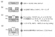
- the figure explaining the device manufacturing process in 1st Embodiment The figure which shows the JV characteristic of the device (PtHf silicide alloy film) manufactured in 1st Embodiment.
- 10A and 10B illustrate a process for forming a CBKR structure.
- FIG. The figure which shows the measurement result of the contact resistance of PtHf silicide alloy film by CBKR method.
- FIG. The figure which shows the analysis result by XRD of the IrYb silicide alloy film of 4th Embodiment.
- First Embodiment a PtHf silicide (Pt x Hf y Si) alloy film in which Pt is used as the metal M1 and Hf is used as the metal M2 is manufactured.
- a PtHf silicide thin film was formed on a Si substrate to manufacture a Schottky diode, and the electrical characteristics of this device were evaluated.
- FIG. 1 shows a device manufacturing process in this embodiment.
- the Si substrate n-Si (100)
- wet oxidation is performed to form a SiO 2 layer
- etching is performed to perform patterning (FIG. 1B).
- a PtHf alloy thin film is formed in the inside (FIG.1 (c)).
- a sintered target made of a PtHf alloy was used for the formation of the PtHf alloy thin film.
- This sintered target is obtained by sintering a fine powder of a PtHf alloy.
- the PtHf alloy powder is manufactured as a powder by melting and alloying high purity Pt and Hf ingots by arc melting to produce a button-shaped ingot, which is mechanically pulverized.
- this alloy powder was sintered with an HIP apparatus under conditions of 1000 kgf / cm 2 , 1500 ° C. and 1 hour to obtain an alloy target (dimensions: diameter 76.2 mm, thickness 2.0 mm).
- the substrate surface was cleaned by preliminary sputtering (output 100 W, 5 minutes). Thereafter, a PtHf alloy was sputtered. The conditions at this time were room temperature and an output of 40 W, and an alloy thin film was formed to a thickness of 20 nm.
- Ar and Kr were used as gas ions in sputtering (both pressures in the apparatus were set to 0.7 Pa).
- silicidation was performed by heat treatment.
- the silicidation conditions were set at three processing temperatures of 450 ° C., 500 ° C., and 600 ° C.
- the treatment atmosphere was nitrogen gas, and the treatment time was 5 minutes.
- Comparative Example 1 As a comparative example for the first embodiment, a Pt thin film was formed instead of PtHf, and this was silicided to manufacture a device.
- the silicidation conditions were basically the same as in the first embodiment (only Ar sputtering was performed).
- the electrical characteristics of the devices manufactured above were evaluated.
- the evaluation test was performed by measuring current density-voltage characteristics (JV characteristics) with a semiconductor parameter analyzer.
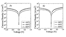
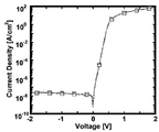
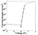
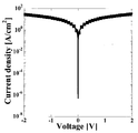
- FIG. 2 shows the JV characteristics of the device (PtHf silicide alloy film) manufactured in this embodiment. From this result, the device manufactured in this embodiment showed a linear increase in current density with respect to voltage application in either the forward direction or the reverse direction (plus direction / minus direction). In this embodiment, although the substrate is n-Si and the behavior at a negative potential is important, it can be said that the device of this embodiment showed good characteristics. On the other hand, the JV characteristics of Comparative Example 1 are shown in FIG.
- the current density was high at 450 ° C.
- the Kr sputtering treatment also had a high current density at 450 ° C.
- the Schottky barrier height of each silicide alloy film was calculated from the measured JV characteristics and summarized in Table 1 below. From Table 1, the Schottky barrier height of the PtHf silicide of this embodiment is 0.47 to 0.51 eV, whereas the Pt silicide of the comparative example is 0.85 eV (Ar sputter). The difference in the Schottky barrier heights of these silicides is due to the work function of the metal to be silicided. In the comparative example, the work function of Pt is high, so it can be said that the Schottky barrier height is increased.
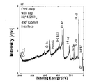
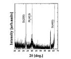
- FIG. 5 shows the result of X-ray diffraction analysis (XRD) of the PtHf silicide alloy film (heat treatment temperature 450 ° C.) of the present embodiment.
- XRD X-ray diffraction analysis
- the root mean square roughness (RMS) of the PtHf silicide alloy film heat treatment temperature 450 ° C.
- AFM atomic force microscope
- the surface formed by Ar sputtering was 2 .16 nm.
- the surface formed by Kr sputtering was 0.45 nm. All showed good surface morphology.
- the RMS of the Pt silicide film as a comparative example was 6.40 nm.
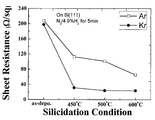
- Second Embodiment A test for evaluating heat resistance in the case of applying high-temperature treatment was performed on the silicidation conditions of the PtHf alloy thin film.
- a cleaned n-Si (111) substrate was prepared, and a PtHf alloy thin film was formed under the same conditions as in the first embodiment (with preliminary sputtering, film thickness 20 nm). This was heat-treated at 400 ° C., 500 ° C., and 600 ° C., and etched with diluted aqua regia to prepare a sample. Then, the sheet resistance of these samples was measured by a four-probe measurement method.
- the measurement results are shown in FIG.
- the PtHf alloy thin film immediately after film formation has a high sheet resistance, but the sheet resistance decreases due to silicidation.
- the sheet resistance of silicide remains low even when processed at a high temperature of 600 ° C.
- PtHf has good thermal stability and that resistance does not increase even at high temperatures.
- FIG. 7 schematically illustrates the process of forming the CBKR structure.
- FIG. 8 shows the measurement results of contact resistance according to the contact area of the PtHf silicide alloy film by the CBKR method. From this evaluation result, it can be seen that the contact resistance of the PtHf silicide alloy film at 2 ⁇ m square has achieved a low resistance of 8 ⁇ 10 ⁇ 8 ⁇ cm. It was confirmed that the application to real devices can be expected.
- an IrYb silicide alloy film (Ir x Yb y Si) in which Ir (work function: 5.27 eV) is applied as the metal M1 and Yb (work function: 2.6 eV) is applied as the metal M2.
- Ir work function: 5.27 eV
- Yb work function: 2.6 eV
- the device manufacturing process is basically the same as in the first embodiment (FIG. 1). After cleaning the Si substrate (n-Si (100)), the SiO 2 layer was formed and etched for patterning. Then, after forming a Yb thin film therein, an Ir thin film was formed and heat-treated to form an IrYb silicide alloy film.
- Yb thin film and Ir thin film were formed using targets made of Ir and Yb metals.
- a Yb melting target (dimensions: diameter 76.1 mm, thickness 2 mm) prepared by cold rolling, annealing, and machining the Yb cast ingot was prepared. Further, an Ir cast ingot obtained by plasma melting was hot forged and hot rolled, and after laser cutting, it was finally finished by cutting and polishing to prepare an Ir melting target.
- the substrate surface was cleaned by preliminary sputtering (output: 100 W, 5 minutes). Then, a Yb thin film and an Ir thin film were formed by RF magnetron sputtering at a Kr gas pressure of 0.65 Pa. The Yb thin film was formed by depositing Yb having a thickness of 6 nm at room temperature and an output of 180 W.
- the film formation conditions for the Ir thin film following the Yb film formation were as follows: room temperature, output 80 W, and 14 nm film formation.
- a cap layer made of an HfN thin film is formed on the thin film, and then a heat treatment is performed to form a silicide alloy film.
- the cap layer was formed by reactive sputtering (RF magnetro sputtering, room temperature, output 200 W) using a Hf target and a film formation atmosphere of Kr / N 2 (film thickness 10 nm).
- the silicidation conditions were a processing temperature of 500 ° C., a processing atmosphere in nitrogen gas, and a processing time of 1 minute. After silicidation, the cap layer and unreacted metal were removed by etching, and an Al electrode was formed to obtain a device.
- Comparative Example 2 As a comparative example for the fourth embodiment, only an Ir thin film was formed and silicided to produce a device. Ir film formation conditions, silicidation conditions, and the like were the same as those in the fourth embodiment.
- FIG. 9 shows the JV characteristics of the device (IrYb silicide alloy film) manufactured in the fourth embodiment. A linear increase in current density was observed for both forward and reverse (positive and negative) voltage applications. On the other hand, the JV characteristics of the device of Comparative Example 2 are shown in FIG. 10, but no increase in current density was observed when a negative potential was applied.
- the Schottky barrier height of the silicide alloy film (IrYb silicide alloy film) of the fourth embodiment was 0.47 eV.
- the height of the Schottky barrier of the silicide alloy film (Ir silicide alloy film) of Comparative Example 2 was 0.89 eV. It was confirmed that the Ir silicide film of Comparative Example 2 has a high Schottky barrier height due to a high Ir work function, and the Schottky barrier height decreases in the fourth embodiment in which Yb is alloyed with Ir. .
- the fourth embodiment was 63.0 ⁇ / sq, and the comparative example 2 was 63.6 ⁇ / sq. As a result, it was confirmed that the sheet resistance of the fourth embodiment slightly decreased.
- FIG. 11 shows the XRD result of the IrYb silicide alloy film of the fourth embodiment.
- the peak of Yb silicide (Yb 5 Si 3 ) seems to be recorded.
- the peak intensity ratio ((Y + Z) / X) of each silicide was about 0.05.
- the Ir x Yb y Si mixed crystal observed by XRD is a mixed crystal (Ir 1-z Yb z Si) formed by replacing Yb with a part of Ir site of Ir silicide (IrSi).
- IrSi Ir silicide
- a PdYb silicide alloy film (Pd x Yb y Si) in which Pd (work function: 4.9 eV) is applied as the metal M1 and Yb (work function: 2.6 eV) is applied as the metal M2.
- Pd work function: 4.9 eV
- Yb work function: 2.6 eV
- a device having A Yb thin film was formed on a Si substrate prepared in the same manner as in the fourth embodiment, and then a Pd thin film was formed and heat treated to form a PdYb silicide alloy film.
- a target made of each metal of Pd and Yb was used.
- the same Yb target as in the fourth embodiment was used.
- a Pd cast ingot obtained by melting in the atmosphere was hot forged and hot rolled, and after laser cutting, was finally finished by cutting and polishing to prepare a Pd melting target.
- the Yb thin film and the Pd thin film were formed by RF magnetro sputtering at a Kr gas pressure of 0.65 Pa.
- the Yb thin film was formed by depositing Yb having a thickness of 6 nm at room temperature and an output of 180 W.
- the film formation conditions for the Pd thin film following the Yb film formation were 14 nm with a room temperature and an output of 80 W.
- silicidation was performed by heat treatment after the formation of the Yb thin film and the Pd thin film and the cap layer.
- the silicidation conditions were a processing temperature of 500 ° C., a processing atmosphere in nitrogen gas, and a processing time of 1 minute. After silicidation, the cap layer and unreacted metal were removed by etching, and an Al electrode was formed to obtain a device.
- Comparative Example 3 As a comparative example for the fifth embodiment, only a Pd thin film was formed and silicided to manufacture a device. The conditions for forming the Pd thin film, the conditions for silicidation, and the like were the same as in the fifth embodiment.
- FIG. 12 shows the JV characteristics of the device (PdYb silicide alloy film) manufactured in the fifth embodiment.
- FIG. 13 shows the JV characteristics of the device of Comparative Example 3. The device of this embodiment also showed a linear increase in current density with respect to voltage application in both forward and reverse directions (plus direction and minus direction). In contrast, the device of Comparative Example 3 did not show an increase in current density when a negative potential was applied.
- the Schottky barrier height of the silicide alloy film (PdYb silicide alloy film) of the fifth embodiment was 0.4 eV.
- the Schottky barrier height of the silicide alloy film (Pd silicide alloy film) of Comparative Example 3 was 0.73 eV. It was confirmed that the Pd silicide film of Comparative Example 3 has a high Schdky barrier height due to a high Pd work function, and the Schottky barrier height decreases in the fifth embodiment in which Yb is alloyed with Pd. .
- the sheet resistance of the silicide film of the fifth embodiment and the comparative example 3 was measured by the four-probe measurement method, the fifth embodiment was 20.9 ⁇ / sq, and the comparative example 2 was 27 ⁇ / sq. Therefore, it was confirmed that the sheet resistance of the fifth embodiment was lowered.
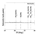
- the XRD result of the PdYb silicide alloy film of the fifth embodiment is shown in FIG.
- the peak of Pd silicide (Pd 2 Si) seems to be recorded.
- the peak intensity ratio ((Y + Z) / X) of each silicide was about 0.05.
- the Pd x Yb y Si mixed crystal observed by this XRD is a mixed crystal (Pd 2-z Yb z Si) formed by substituting Yb for a part of Pd sites of Pd silicide (Pd 2 Si). )Met.
- a PdEr silicide alloy film (Pd x Er y Si) in which Pd (work function: 4.9 eV) is applied as the metal M1 and Er (work function: 3.2 eV) is applied as the metal M2.
- Pd work function: 4.9 eV
- Er work function: 3.2 eV
- a sintered target made of a PdEr alloy was used, a PdEr alloy thin film was formed, and then heat treatment for silicidation was performed to confirm the success or failure of silicidation.
- a sintered target made of a PdEr alloy is obtained by sintering a fine powder of a PdEr alloy.
- the PdEr alloy powder is manufactured as a powder by melting and alloying high purity Pd and Er ingots by arc melting to produce a button-shaped ingot, which is mechanically pulverized.
- the surface of the n-Si (100) substrate was first cleaned by pre-sputtering (output 200 W, 30 minutes) and washed. Thereafter, a PdEr alloy film was sputtered. The conditions at this time were room temperature, output 80 W, 0.65 Pa, and the sputtering gas was Kr gas. Then, a 20 nm PdEr alloy thin film was formed.
- an HfN cap layer was formed and heat-treated for silicidation.
- the cap layer was formed by reactive sputtering (RF magnetro sputtering, room temperature, output 200 W) using a Hf target and a film formation atmosphere of Kr / N 2 (film thickness 20 nm).
- RF magnetro sputtering room temperature, output 200 W
- a film formation atmosphere of Kr / N 2 film thickness 20 nm.
- the processing temperature was 550 ° C.
- the processing atmosphere was in nitrogen gas
- the processing time was 30 minutes.
- the cap layer and unreacted metal were removed by etching.
- FIG. 15 shows the XRD result of the PdEr silicide alloy film manufactured in the above process.
- the peaks of Pd silicide and Er silicide were extremely weak.
- the peak intensity ratio ((Y + Z) / X) of each silicide was less than 0.01.
- the Pd x Er y Si mixed crystal observed by XRD is a mixed crystal (Pd 2 ⁇ z Er z Si) formed by substituting Er at a part of Pd sites of Pd silicide (Pd 2 Si). )Met.
- the silicide alloy film according to the present invention is made of silicide of the metal M1 and the metal M2 having different work functions, and has good thermal stability, and has a work function near midgap with respect to the Si substrate. Have.
- the present invention is suitable as a constituent material for silicide electrodes in various semiconductor devices such as MOSFETs.
Landscapes
- Chemical & Material Sciences (AREA)
- Organic Chemistry (AREA)
- Engineering & Computer Science (AREA)
- Materials Engineering (AREA)
- Mechanical Engineering (AREA)
- Metallurgy (AREA)
- Chemical Kinetics & Catalysis (AREA)
- Inorganic Chemistry (AREA)
- Physics & Mathematics (AREA)
- Thermal Sciences (AREA)
- General Chemical & Material Sciences (AREA)
- Electrodes Of Semiconductors (AREA)
- Internal Circuitry In Semiconductor Integrated Circuit Devices (AREA)
- Physical Vapour Deposition (AREA)
Abstract
Description
第1実施形態:本実施形態では、金属M1としてPtを金属M2としてHfを適用する、PtHfシリサイド(PtxHfySi)合金膜を製造した。ここでは、Si基板にPtHfシリサイド薄膜を形成してショットキーダイオードを製造し、このデバイスの電気特性を評価した。

Claims (8)
- Siを含む基板上に形成されるシリサイド合金膜において、
仕事関数が4.6eV以上5.7eV以下の金属M1と、仕事関数が2.5eV以下4.0eV以上の金属M2と、Siとからなり、
4.3eV以上4.9eV以下の仕事関数を有することを特徴とするシリサイド合金膜。 - 金属M1は、Pt、Pd、Mo、Ir、W、又はRuの少なくともいずれかである請求項1記載のシリサイド合金膜。
- 金属M2は、Hf、La、Er、Ho、Er、Eu、Pr、又はSmの少なくともいずれかである請求項1又は請求項2記載のシリサイド合金膜。
- Si含有量が33at%以上50at%以下である請求項1~請求項3のいずれかに記載のシリサイド合金膜。
- X線回折分析により観察される、金属M1と金属M2とSiとからなる混晶体(M1xM2ySi)の回折ピークのピーク強度(X)と、金属M1のシリサイド(M1aSi)の回折ピークのピーク強度(Y)と、金属M2のシリサイド(M2bSi)の回折ピークのピーク強度(Z)と、の関係について、
Xに対する、YとZとの和の比率((Y+Z)/X)が0.1以下である請求項1~請求項4のいずれかに記載のシリサイド合金膜。 - 不純物であるC、Oの濃度が合計で5質量%以下である請求項1~請求項5のいずれかに記載のシリサイド合金膜。
- 自乗平均表面粗さ(RMS)が5nm以下である請求項1~請求項6のいずれかに記載のシリサイド合金膜。
- 請求項1~請求項7のいずれかに記載のシリサイド合金膜の製造方法であって、
Si基板の上に金属M1と金属M2とからなる薄膜を形成した後、
前記Si基板を熱処理して金属M1及び金属M2をシリサイド化するシリサイド合金膜の製造方法。
Priority Applications (3)
| Application Number | Priority Date | Filing Date | Title |
|---|---|---|---|
| US15/573,770 US10246770B2 (en) | 2015-06-26 | 2016-06-24 | Silicide alloy film for semiconductor device electrode, and production method for silicide alloy film |
| JP2017524988A JP6455847B2 (ja) | 2015-06-26 | 2016-06-24 | 半導体デバイス電極用のシリサイド合金膜及びシリサイド合金膜の製造方法 |
| KR1020177035200A KR102012118B1 (ko) | 2015-06-26 | 2016-06-24 | 반도체 디바이스 전극용의 실리사이드 합금막 및 실리사이드 합금막의 제조 방법 |
Applications Claiming Priority (2)
| Application Number | Priority Date | Filing Date | Title |
|---|---|---|---|
| JP2015128774 | 2015-06-26 | ||
| JP2015-128774 | 2015-06-26 |
Publications (1)
| Publication Number | Publication Date |
|---|---|
| WO2016208704A1 true WO2016208704A1 (ja) | 2016-12-29 |
Family
ID=57585861
Family Applications (1)
| Application Number | Title | Priority Date | Filing Date |
|---|---|---|---|
| PCT/JP2016/068768 Ceased WO2016208704A1 (ja) | 2015-06-26 | 2016-06-24 | 半導体デバイス電極用のシリサイド合金膜及びシリサイド合金膜の製造方法 |
Country Status (5)
| Country | Link |
|---|---|
| US (1) | US10246770B2 (ja) |
| JP (1) | JP6455847B2 (ja) |
| KR (1) | KR102012118B1 (ja) |
| TW (1) | TWI612146B (ja) |
| WO (1) | WO2016208704A1 (ja) |
Families Citing this family (2)
| Publication number | Priority date | Publication date | Assignee | Title |
|---|---|---|---|---|
| KR102618541B1 (ko) * | 2016-08-04 | 2023-12-28 | 삼성전자주식회사 | 이차원 물질층을 포함하는 전자 소자 |
| CN110112222A (zh) * | 2019-06-10 | 2019-08-09 | 吉林麦吉柯半导体有限公司 | 一种沟槽肖特基二极管及制作方法 |
Citations (4)
| Publication number | Priority date | Publication date | Assignee | Title |
|---|---|---|---|---|
| JPH0738104A (ja) * | 1993-07-22 | 1995-02-07 | Toshiba Corp | 半導体装置の製造方法 |
| JP2007173412A (ja) * | 2005-12-20 | 2007-07-05 | Toshiba Corp | 半導体装置 |
| JP2008060101A (ja) * | 2006-08-29 | 2008-03-13 | Toshiba Corp | 半導体装置およびその製造方法 |
| JP2009277961A (ja) * | 2008-05-16 | 2009-11-26 | Renesas Technology Corp | Cmisトランジスタの製造方法 |
Family Cites Families (1)
| Publication number | Priority date | Publication date | Assignee | Title |
|---|---|---|---|---|
| KR101021488B1 (ko) | 2004-03-01 | 2011-03-16 | Jx닛코 닛세끼 킨조쿠 가부시키가이샤 | 니켈-플라티늄 합금 및 동(同) 합금 타겟트 |
-
2016
- 2016-06-24 TW TW105119891A patent/TWI612146B/zh not_active IP Right Cessation
- 2016-06-24 US US15/573,770 patent/US10246770B2/en active Active
- 2016-06-24 WO PCT/JP2016/068768 patent/WO2016208704A1/ja not_active Ceased
- 2016-06-24 JP JP2017524988A patent/JP6455847B2/ja not_active Expired - Fee Related
- 2016-06-24 KR KR1020177035200A patent/KR102012118B1/ko active Active
Patent Citations (4)
| Publication number | Priority date | Publication date | Assignee | Title |
|---|---|---|---|---|
| JPH0738104A (ja) * | 1993-07-22 | 1995-02-07 | Toshiba Corp | 半導体装置の製造方法 |
| JP2007173412A (ja) * | 2005-12-20 | 2007-07-05 | Toshiba Corp | 半導体装置 |
| JP2008060101A (ja) * | 2006-08-29 | 2008-03-13 | Toshiba Corp | 半導体装置およびその製造方法 |
| JP2009277961A (ja) * | 2008-05-16 | 2009-11-26 | Renesas Technology Corp | Cmisトランジスタの製造方法 |
Also Published As
| Publication number | Publication date |
|---|---|
| TWI612146B (zh) | 2018-01-21 |
| JPWO2016208704A1 (ja) | 2018-04-12 |
| US20180148830A1 (en) | 2018-05-31 |
| TW201704495A (zh) | 2017-02-01 |
| US10246770B2 (en) | 2019-04-02 |
| JP6455847B2 (ja) | 2019-01-23 |
| KR20180005208A (ko) | 2018-01-15 |
| KR102012118B1 (ko) | 2019-08-19 |
Similar Documents
| Publication | Publication Date | Title |
|---|---|---|
| CN105018889B (zh) | 含钼靶材 | |
| JP6276327B2 (ja) | モリブデンを含有した標的 | |
| TWI523087B (zh) | Al alloy film for semiconductor devices | |
| JP2011523978A (ja) | モリブデン−ニオブ合金、かかる合金を含有するスパッタリングターゲット、かかるターゲットの製造方法、それから製造される薄膜、およびその使用 | |
| JP6455847B2 (ja) | 半導体デバイス電極用のシリサイド合金膜及びシリサイド合金膜の製造方法 | |
| JP6126648B2 (ja) | 白金合金ターゲット | |
| TWI609415B (zh) | 半導體裝置電極的製造方法 | |
| JP2012243878A (ja) | 半導体電極構造 | |
| JP2017092330A (ja) | デバイス用配線膜 | |
| Lim et al. | Suppression of Size Effect in MoPd Thin Films for Nanoscale Interconnects | |
| JP2017092331A (ja) | デバイス用配線膜、およびAl合金スパッタリングターゲット材料 | |
| JP2012243877A (ja) | 半導体電極構造 | |
| JP4543012B2 (ja) | 高純度Ti−W材から成るターゲット | |
| TW466693B (en) | Manufacture method of metal salicide | |
| JP2016219531A (ja) | パワー半導体素子用Al合金膜 | |
| CN101499488A (zh) | 半导体器件及其制造方法 | |
| KR20080024374A (ko) | Ulsi을 위한 고온 안정 니켈 실리사이드 제조방법 | |
| JP2005026704A (ja) | 半導体素子の製造方法およびマグネトロンスパッタリング装置用Ti−W材 | |
| JP2006287253A (ja) | 半導体素子の製造方法 | |
| JP2005020020A (ja) | 半導体素子の製造方法およびマグネトロンスパッタリング装置用Ti材の製造方法 |
Legal Events
| Date | Code | Title | Description |
|---|---|---|---|
| 121 | Ep: the epo has been informed by wipo that ep was designated in this application |
Ref document number: 16814473 Country of ref document: EP Kind code of ref document: A1 |
|
| ENP | Entry into the national phase |
Ref document number: 2017524988 Country of ref document: JP Kind code of ref document: A |
|
| WWE | Wipo information: entry into national phase |
Ref document number: 15573770 Country of ref document: US |
|
| ENP | Entry into the national phase |
Ref document number: 20177035200 Country of ref document: KR Kind code of ref document: A |
|
| NENP | Non-entry into the national phase |
Ref country code: DE |
|
| 122 | Ep: pct application non-entry in european phase |
Ref document number: 16814473 Country of ref document: EP Kind code of ref document: A1 |