WO2016208643A1 - 非可逆回路素子、高周波回路及び通信装置 - Google Patents
非可逆回路素子、高周波回路及び通信装置 Download PDFInfo
- Publication number
- WO2016208643A1 WO2016208643A1 PCT/JP2016/068578 JP2016068578W WO2016208643A1 WO 2016208643 A1 WO2016208643 A1 WO 2016208643A1 JP 2016068578 W JP2016068578 W JP 2016068578W WO 2016208643 A1 WO2016208643 A1 WO 2016208643A1
- Authority
- WO
- WIPO (PCT)
- Prior art keywords
- yoke
- surface side
- circuit device
- permanent magnets
- mounting surface
- Prior art date
- Legal status (The legal status is an assumption and is not a legal conclusion. Google has not performed a legal analysis and makes no representation as to the accuracy of the status listed.)
- Ceased
Links
Images









Classifications
-
- H—ELECTRICITY
- H01—ELECTRIC ELEMENTS
- H01P—WAVEGUIDES; RESONATORS, LINES, OR OTHER DEVICES OF THE WAVEGUIDE TYPE
- H01P1/00—Auxiliary devices
- H01P1/32—Non-reciprocal transmission devices
- H01P1/38—Circulators
- H01P1/383—Junction circulators, e.g. Y-circulators
Definitions
- the present invention relates to non-reciprocal circuit elements, particularly non-reciprocal circuit elements such as circulators and isolators used in the microwave band, and further relates to a high-frequency circuit and a communication apparatus including the elements.
- non-reciprocal circuit elements such as circulators and isolators have a characteristic of transmitting signals only in a predetermined specific direction and not transmitting in the reverse direction.
- a circulator is used in a transmission / reception circuit unit of a mobile communication device such as a mobile phone.
- Patent Document 1 includes a ferrite plate having a plurality of strip lines, a plurality of magnets arranged around the side surface of the ferrite plate, and two yoke plates arranged to sandwich the ferrite plate.
- a non-reciprocal circuit device provided is described.
- a thin (low profile) is achieved by arranging a magnet on the side of the ferrite plate.
- non-reciprocal circuit elements in which magnets are arranged on the side surface of ferrite are also described in Patent Documents 2 and 3, for example.
- FIG. 1 The general structure of this type of nonreciprocal circuit device is shown in FIG.
- Permanent magnets 131 and 132 are arranged on the side surface side of the magnetic rotor 110 made of the ferrite 120 including the central conductor, and yokes 151 and 152 are arranged on the top surface side and the mounting surface side of the magnetic rotor 110.
- the end portions of the yokes 151 and 152 extend to the end surfaces of the permanent magnets 131 and 132 in plan view, and therefore, the leakage flux ⁇ 2 in addition to the flux ⁇ 1 that passes through the ferrite 120.
- the magnetic efficiency by the permanent magnets 131 and 132 is reduced.
- An object of the present invention is to provide a non-reciprocal circuit element, a high-frequency circuit, and a communication device that can achieve a low profile and can suppress a decrease in magnetic efficiency due to a permanent magnet as much as possible.
- the nonreciprocal circuit device is A plurality of central conductors are arranged in the ferrite, and a magnetic rotor having a top surface, a mounting surface, and side surfaces; A permanent magnet disposed on a side surface of the magnetic rotor; Yokes respectively disposed on the top surface side and the mounting surface side of the magnetic rotor;
- a non-reciprocal circuit device comprising: An end of at least one of the top surface side yoke and the mounting surface side yoke overlaps with the permanent magnet in a plan view and exists inside the end surface of the permanent magnet; It is characterized by.
- a high-frequency circuit according to a second aspect of the present invention includes the non-reciprocal circuit element and a power amplifier. It is characterized by.
- a communication device includes the non-reciprocal circuit element and the RFIC. It is characterized by.
- the permanent magnet is disposed on the side surface side of the magnetic rotor, a reduction in height is achieved, and at least one of the top surface side yoke and the mounting surface side yoke is provided. Since the end portion overlaps with the permanent magnet and is present on the inner side of the end surface of the permanent magnet in plan view, the leakage magnetic flux is reduced, and the decrease in magnetic efficiency is suppressed as much as possible.
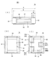
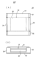
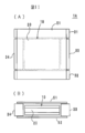
- positioning relationship between a permanent magnet and a yoke is shown, (A) is a top view, (B) is an elevation view.
- positioning relationship between a permanent magnet and a yoke is shown, (A) is a top view, (B) is an elevation view.
- positioning relationship between a permanent magnet and a yoke is shown, (A) is a top view, (B) is an elevation view.
- positioning relationship between a permanent magnet and a yoke is shown, (A) is a top view, (B) is an elevation view.
- positioning relationship between a permanent magnet and a yoke is shown, (A) is a top view, (B) is an elevation view.
- positioning relationship between a permanent magnet and a yoke is shown, (A) is a top view, (B) is an elevation view. It is explanatory drawing of the manufacture example (top
- the nonreciprocal circuit device 1A is a lumped constant type three-port circulator having the equivalent circuit shown in FIG. That is, the first center conductor 21 (L1), the second center conductor 22 (L2), and the third center conductor 23 (L3) are respectively insulated from the ferrite 20 to which a DC magnetic field is applied in the arrow A direction by a permanent magnet. It is arranged to intersect at an angle of.
- One end of the first center conductor 21 is a first port P1
- one end of the second center conductor 22 is a second port P2
- one end of the third center conductor 23 is a third port P3.
- the other ends of the center conductors 21, 22, and 23 are connected to the ground.
- capacitive elements C1, C2, and C3 are connected in parallel to the central conductors 21, 22, and 23, respectively.
- one end of the first center conductor 21 is an external connection electrode 41, the other end is an external connection electrode 42, one end of the second center conductor 22 is an external connection electrode 43, and the other end is an external connection electrode 44.
- One end of the third center electrode 23 is an external connection electrode 45 and the other end is an external connection electrode 46.
- the operation of the non-reciprocal circuit element 1A (3-port circulator) in the transmission / reception circuit section is as follows. That is, the high frequency signal input from the first port P1 (transmission circuit TX) is output from the third port P3 (antenna ANT), and the high frequency signal input from the third port P3 (antenna ANT) is the second port P2. (Receiver circuit RX).
- the high frequency signal of the second port P2 is not attenuated by the transmission / reception circuit unit and transmitted to the first port P1.
- the non-reciprocal circuit element 1A includes a magnetic rotor 10 shown in FIG.
- This magnetic rotor 10 is formed by laminating insulator layers 11, 12, 13, 14 mainly composed of glass, various conductors, and various electrodes on the top surface side and the mounting surface side of a rectangular microwave ferrite 20.
- the ferrite 20 is also formed with a plurality of through-hole conductors and a plurality of electrodes for connecting various conductors provided on the top surface side and the mounting surface side in a coil shape.
- the conductors 21a, 21b, and 21c forming the first central conductor 21 (L1) are formed on the insulator layer 12, and the conductors 21d and 21e are formed between the insulator layer 13 and the ferrite 20.
- An end portion of the conductor 21a is an external lead portion 41a
- an end portion of the conductor 21c is an external lead portion 42a.
- the other end of the conductor 21a is connected to one end of the conductor 21d via the conductor 21f
- the other end of the conductor 21d is connected to one end of the conductor 21b via the conductor 21g.
- the other end of the conductor 21b is connected to one end of a conductor 21e via a conductor 21h
- the other end of the conductor 21e is connected to one end of a conductor 21c via a conductor 21i.
- the conductors 22a, 22b, and 22c forming the second central conductor 22 (L2) are formed between the insulator layer 11 and the ferrite 20, and the conductors 22d and 22e are formed on the lower surface of the insulator layer 14.
- An end portion of the conductor 22a is an external lead portion 43a
- an end portion of the conductor 22c is an external lead portion 44a.
- the other end of the conductor 22a is connected to one end of the conductor 22d via the conductor 22f, and the other end of the conductor 22d is connected to one end of the conductor 22b via the conductor 22g.
- the other end of the conductor 22b is connected to one end of a conductor 22e via a conductor 22h, and the other end of the conductor 22e is connected to one end of a conductor 22c via a conductor 22i.
- the conductors 23a, 23b and 23c forming the third central conductor 23 (L3) are formed between the insulator layers 11 and 12, and the conductors 23d and 23e are formed between the insulator layers 13 and 14.
- An end portion of the conductor 23a is an external lead portion 46a
- an end portion of the conductor 23c is an external lead portion 45a.
- the other end of the conductor 23a is connected to one end of the conductor 23d through the conductor 23f, and the other end of the conductor 23d is connected to one end of the conductor 23b through the conductor 23g.
- the other end of the conductor 23b is connected to one end of a conductor 23e through a conductor 23h, and the other end of the conductor 23e is connected to one end of a conductor 23c through a conductor 23i.
- the external connection electrode 41 is formed by an external lead portion 41a which is an end portion of the conductor 21a and an electrode connected thereto.
- the external connection electrode 42 is formed by an external lead portion 42a which is an end portion of the conductor 21c and an electrode connected thereto.
- the external connection electrode 43 is formed by an external lead portion 43a which is an end portion of the conductor 22a and an electrode connected thereto.
- the external connection electrode 44 is formed by an external lead portion 44a, which is an end portion of the conductor 22c, and an electrode connected thereto.
- the external connection electrode 45 is formed by an external lead portion 45a which is an end portion of the conductor 23c and an electrode connected thereto.
- the external connection electrode 46 is formed by an external lead portion 46a, which is an end portion of the conductor 23a, and an electrode connected thereto.
- the central conductors 21, 22, and 23 can be formed as thin film conductors such as Ag and Cu, thick film conductors, or conductive foils, and it is preferable to use a photosensitive metal paste.
- the insulator layers 11 to 14 are preferably made of a material having high insulation resistance such as photosensitive glass or polyimide.
- the conductor layer and the insulating layer can be formed by photolithography, etching, printing, or the like.
- the external connection electrodes 41 to 46 and the through-hole conductors are preferably formed by applying and baking a conductive electrode material (paste) mainly composed of Ag and Cu, and forming a Ni plating layer on the surface thereof. Further, a plating layer of Au, Sn, Ag, Cu or the like is formed. It is not limited to plating, but may be a sputtering process or the like.
- the capacitive elements C1, C2, C3 use chip parts.
- the magnetic rotor 10 having the above configuration has permanent magnets 31 to 34 disposed on four side surfaces, a yoke 51 disposed on the top surface side, and a yoke 52 disposed on the mounting surface side.
- the nonreciprocal circuit element 1A is obtained.
- the yokes 51 and 52 are preferably made of a magnetic material such as SPCC, and may be a single metal of Fe, Ni, Co or an alloy containing these as a main component.
- a plated layer of Ag or Au may be formed on the surfaces of the yokes 51 and 52 in order to reduce high frequency loss.
- the magnetic rotor 10 and the permanent magnets 31 to 34 are integrated with a resin (not shown) as an adhesive while being sandwiched between the yokes 51 and 52. That is, the gap portion shown in FIG. 3A is filled with resin.
- the structure in which the permanent magnets 31 to 34 are arranged on the side surface side of the magnetic rotor 10 and the upper and lower surfaces are sandwiched between the yokes 51 and 52 is referred to as a ferrite / magnet assembly in this specification.
- the mounting surface side yoke 52 is divided into a plurality of segments 52a, 52b, 52c, and 52d, and the electrodes 41 (first ports P1, TX) are formed on the segments 52a.
- the electrode 43 (second port P2, RX) is connected to the segment 52b, and the electrode 45 (third port P3, ANT) is connected to the segment 52c.
- the electrodes 42, 44, and 46 (GND) are connected to the segment 52d. That is, the electrodes 41 to 46 of the magnetic rotor 10 are connected to a transmission circuit, a reception circuit, an antenna, and the like via segments 52a, 52b, 52c, and 52d that are divided in an electrically insulated state.
- the important point in the first embodiment is that the end portions of the yokes 51 and 52 overlap with the permanent magnets 31 to 34 in a plan view and exist inside the end surfaces of the permanent magnets 31 to 34. Therefore, as shown in FIG. 23A, the magnetic flux leaking to the outside from the ends of the yokes 51 and 52 (leakage magnetic flux ⁇ 2 shown in the conventional example of FIG. 23B) is almost eliminated, and most of the magnetic flux is converted into the ferrite 20. (Magnetic flux ⁇ 1), and the magnetic efficiency is improved.
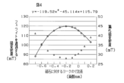
- FIG. 4 shows the magnetic flux density passing through the ferrite 20 (indicated by a circle, see the left vertical axis, hereinafter referred to as effective magnetic flux density) and the leakage magnetic flux (indicated by a triangular mark, see the right vertical axis). Is shown on the basis of the dimensional difference between the yokes 51 and 52 (shown as a dimensional difference on both sides, half of which is on one side). That is, when the distance between the end portions of the yoke 51 (52) is C and the distance between the end surfaces of the pair of permanent magnets 31, 32 (33, 34) is D, the difference (C ⁇ D) is the horizontal axis. . According to FIG.
- the dimension difference of 0 mm is the conventional example shown in FIG. 23B, and the magnetic flux density passing through the ferrite 20 at that time is about 115 mT, and the leakage magnetic flux is about 30 mT.
- the effective magnetic flux density has a maximum value when the dimensional difference (CD) is -0.2 mm (-0.1 mm on one side), and this maximum value is a region where the change in magnetic flux density is small, and is robust in mass-produced products. Is expensive.
- the leakage flux takes a minimum value when the dimensional difference (CD) is -0.2 mm (-0.1 mm on one side), and since this minimum value has little magnetic influence on the peripheral circuit elements, it can be used for high-density mounting. Contribute.
- the effective magnetic flux density is larger than about 115 mT and the leakage magnetic flux is smaller than about 30 mT when the dimensional difference (CD) is 0 mm to ⁇ 0.4 mm. Therefore, it is preferable that ⁇ 0.4 mm ⁇ (CD) ⁇ 0 mm.
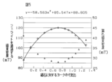
- FIG. 5 shows the effective magnetic flux density (indicated by a circle, see the left vertical axis) and the leakage magnetic flux (indicated by a triangular mark, see the right vertical axis) based on the dimensional ratio between the yokes 51 and 52 and the permanent magnets 31 to 34. It shows. That is, when the width dimension of the permanent magnets 31 to 34 is B and the width dimension where the end portions of the yokes 51 and 52 overlap with the permanent magnets 31 to 34 is A, the dimension ratio (A / B) is the horizontal axis. According to FIG. 5, the dimensional ratio 1.0 is the conventional example shown in FIG.
- the effective magnetic flux density has a maximum value at a dimensional ratio of about 0.7, and the maximum value is a region where the change in the magnetic flux density is small, and the robustness in mass-produced products is high.
- the leakage magnetic flux takes a minimum value at a dimensional ratio of about 0.7, and this minimum value contributes to high-density mounting because there is little magnetic influence on peripheral circuit elements.
- the sizes of the permanent magnets 31 and 32 were 0.35 mm in width, 2.2 mm in length, and 0.48 mm in height.
- the permanent magnets 33 and 34 had a width of 0.35 mm, a length of 1.2 mm, and a height of 0.48 mm.
- the outer sizes of the yokes 51 and 52 were 1.8 mm for the short side and 2.00 mm for the long side.
- the leakage flux is a value at a location 2 mm away from the end faces of the permanent magnets 31-34.
- the magnetic rotor 10 does not necessarily have a quadrangular shape in plan view. Further, the permanent magnet and the yoke can take various arrangement relationships.
- one permanent magnet 31 to 34 is arranged on each of the four side surfaces of the magnetic rotor 10, and the end portions of the yokes 51 and 52 are all four sides. Thus, they are positioned inside the end faces of the permanent magnets 31-34. It is sufficient that at least a pair of permanent magnets is disposed, and any one end of the yokes 51 and 52 only needs to be present inside the end surface of the permanent magnet. Below, various examples of this arrangement relationship will be shown.
- FIG. 6 shows a second example.
- the yoke 51 on the top surface side has an end portion on the inner side of the end surfaces of the permanent magnets 33, 31, 32 on one side, and the end portion on the other three sides. It is equal to the end faces of the permanent magnets 34, 31, 32.
- the yoke 52 on the mounting surface side has its ends equal to the end surfaces of the permanent magnets 31 to 34 on four sides.
- FIG. 7 shows a third example
- the yoke 51 on the top surface side has two ends on the inner side of the end surfaces of the permanent magnets 31 to 34, and the other two sides have permanent magnets at the ends. It is equal to the end faces of 31 and 32.
- the yoke 52 on the mounting surface side has its ends equal to the end surfaces of the permanent magnets 31 to 34 on four sides.
- FIG. 8 shows a fourth example
- the yoke 51 on the top surface side has its ends on the inner side of the end surfaces of the permanent magnets 31 to 34 on the two sides, and the other two sides have their ends on the permanent magnet. It is equal to the end faces of 31 and 32.
- the yoke 52 on the mounting surface side has one end on the inner side of the end surfaces of the permanent magnets 33, 31, 32, and the other three sides have end portions on the end surfaces of the permanent magnets 34, 31, 32. Is equal to
- FIG. 9 shows a fifth example.
- the yoke 51 on the top surface side has one end on the inner side of the end surfaces of the permanent magnets 33, 31, 32, and the other three sides have the end portions thereof. It is equal to the end faces of the permanent magnets 34, 31, 32.
- the yoke 52 on the mounting surface side has one end on the inner side of the end surfaces of the permanent magnets 33, 31, 32, and the other three sides have end portions on the end surfaces of the permanent magnets 34, 31, 32. Is equal to
- FIG. 10 shows a sixth example
- the yoke 51 on the top surface side has its end on one side inside the end surfaces of the permanent magnets 33, 31, 32, and its end on the other three sides. It is equal to the end faces of the permanent magnets 34, 31, 32.
- the yoke 52 on the mounting surface side has its ends on the inner side of the end surfaces of the permanent magnets 31 to 34 on the two sides, and the other two sides have the end portions equal to the end surfaces of the permanent magnets 31 and 32.
- FIG. 11 shows a seventh example
- the yoke 51 on the top surface side has its ends on the inner side of the end surfaces of the permanent magnets 31 to 34 on the two sides, and the other two sides have their end portions on the permanent magnet. It is equal to the end faces of 31 and 32.
- the yoke 52 on the mounting surface side has its ends on the inner side of the end surfaces of the permanent magnets 31 to 34 on the two sides, and the other two sides have the end portions equal to the end surfaces of the permanent magnets 31 and 32.
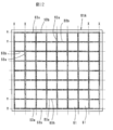
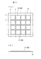
- the ferrite / magnet assembly includes the magnetic rotor 10 and the permanent magnets 31 to 34 between the yokes (collected substrates 51A and 52A) having a large area shown in FIGS. They are arranged in a matrix and cut out so as to form one unit of element 1A.
- slits 53a and 54a are respectively formed in the vertical and horizontal directions so that the end portions of the individual yokes 51 and 52 are disposed on the inner side of the end surfaces of the permanent magnets 31 to 34 in the collective substrates 51A and 52A.
- the bridges 53b and 54b are provided in the slits 53a and 54a so that the yokes 51 and 52 of one unit are not separated.
- the aggregated ferrite-magnet assembly is integrated by filling the aggregate substrates 51A and 52A with a resin material 55 (see FIG. 14) having a relative magnetic permeability of about 1.0, and the aggregate substrates 51A and 52A are illustrated. 12 and the one-dot chain lines X and Y shown in FIG. Filling the resin material 55 integrates the ferrite / magnet assembly and prevents the resin material 55 from reaching the corners of the permanent magnets 31 to 34 and chipping or cracking of the permanent magnets 31 to 34. Is done. By using the resin material 55 having a relative magnetic permeability of 1.0, the leakage magnetic flux does not increase.
- the various electrodes of the magnetic rotor 10 are electrically connected to the segments 52a, 52b, 52c, 52d of the yoke 52 on the mounting surface side via solder 56 (see FIG. 14).
- the nonreciprocal circuit device 1B according to the second embodiment is a lumped constant type three-port circulator having the equivalent circuit shown in FIG. 1 as in the first embodiment, and the nonreciprocal circuit according to the first embodiment. It differs from the element 1A in that the mounting surface side yoke 52 (see FIG. 15C) is not divided into segments and is formed of a single piece, and the other configurations are the same.
- the various electrodes 41 to 46 formed on the magnetic rotor 10 are not connected to the mounting surface side yoke 52 (is insulated from the yoke 52 by a resin material or the like), and the magnetic rotation
- the terminal 10 is electrically connected to a terminal (not shown) from the side surface, and is connected to a transmitting circuit, a receiving circuit, an antenna, and the like through these terminals.
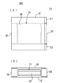
- the end portions of the yokes 51 and 52 overlap with the permanent magnets 31 to 34 in a plan view and exist inside the end surfaces of the permanent magnets 31 to 34 (FIGS. 15B and 15C). ). Therefore, almost no magnetic flux leaks to the outside from the end portions of the yokes 51 and 52, and most of the magnetic flux passes through the ferrite 20, thereby improving the magnetic efficiency. Further, for the relationship between the end portions of the yokes 51 and 52 and the end surfaces of the permanent magnets 31 to 34, for example, various arrangement relationships shown in FIGS. 6 to 11 can be employed.
- the magnetic characteristic is better than that of the first embodiment in that the mounting surface side yoke 52 is one (not divided).
- the magnetic characteristics are shown in FIGS. FIG. 16 corresponds to FIG. 4, and the magnetic flux density passing through the ferrite 20 (indicated by a circle, see the left vertical axis, hereinafter referred to as an effective magnetic flux density) and the leakage magnetic flux (indicated by a triangular mark, see the right vertical axis) Is shown based on the dimensional difference of the yokes 51 and 52 with respect to the magnets 31 to 34 (shown as a dimensional difference on both sides, half of which is on one side).
- the difference (C ⁇ D) is the horizontal axis.
- the dimension difference of 0 mm is the conventional example shown in FIG. 23B, and the magnetic flux density passing through the ferrite 20 at that time is about 120 mT, and the leakage magnetic flux is about 28 mT.
- the effective magnetic flux density has a maximum value when the dimensional difference (CD) is -0.2 mm (-0.1 mm on one side), and this maximum value is a region where the change in magnetic flux density is small, and is robust in mass-produced products. Is expensive.
- the leakage flux takes a minimum value when the dimensional difference (CD) is -0.2 mm (-0.1 mm on one side), and since this minimum value has little magnetic influence on the peripheral circuit elements, it can be used for high-density mounting. Contribute.
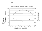
- FIG. 17 shows the effective magnetic flux density (indicated by a circle, see the left vertical axis) and the leakage magnetic flux (indicated by a triangular mark, see the right vertical axis) based on the dimensional ratio between the yokes 51 and 52 and the permanent magnets 31-34. It shows. That is, when the width dimension of the permanent magnets 31 to 34 is B and the width dimension where the end portions of the yokes 51 and 52 overlap with the permanent magnets 31 to 34 is A, the dimension ratio (A / B) is the horizontal axis. According to FIG. 17, the size ratio 1.0 is the conventional example shown in FIG.
- the effective magnetic flux density has a maximum value at a dimensional ratio of about 0.7, and the maximum value is a region where the change in the magnetic flux density is small, and the robustness in mass-produced products is high.
- the leakage magnetic flux takes a minimum value at a dimensional ratio of about 0.7, and this minimum value contributes to high-density mounting because there is little magnetic influence on peripheral circuit elements.
- the sizes of the permanent magnets 31 and 32 were 0.35 mm in width, 2.2 mm in length, and 0.48 mm in height.
- the permanent magnets 33 and 34 had a width of 0.35 mm, a length of 1.2 mm, and a height of 0.48 mm.
- the outer sizes of the yokes 51 and 52 were 1.8 mm for the short side and 2.00 mm for the long side.
- the leakage flux is a value at a location 2 mm away from the end faces of the permanent magnets 31-34.
- the ferrite / magnet assembly includes the magnetic rotor 10 and the permanent magnets 31 to 34 arranged in a matrix between the large area yokes (collected substrates 51A and 52A) shown in FIG. And cut out so as to be one unit of element 1B.
- slits 53a and 54a are respectively formed in the vertical and horizontal directions so that the end portions of the individual yokes 51 and 52 are disposed on the inner side of the end surfaces of the permanent magnets 31 to 34 in the collective substrates 51A and 52A.
- the bridges 53b and 53b are provided in the slits 53a and 54a so that the yokes 51 and 52 of one unit are not separated.
- the aggregated ferrite-magnet assembly is integrated by filling the resin material 55 shown in FIG. 14 between the aggregate substrates 51A and 52A, and the aggregate substrates 51A and 52A are connected to the alternate long and short dashed lines X, By cutting with Y, the element 1B is cut out as one unit.
- the individually separated yokes 51 and 52 are attached to the sheet 57, and this is used as a collective substrate. Also good. Even in this case, the sheet 57 can be cut out along the alternate long and short dash lines X and Y to be cut out as one unit of the element 1B.
- a nonreciprocal circuit device 1C according to the third embodiment is a lumped constant type three-port circulator having the equivalent circuit shown in FIG. 1 as in the first embodiment.
- the end portions thereof are equal to the end surfaces of the permanent magnets 31 to 34 in plan view. That is, the third embodiment is the same as the first embodiment in that the yoke 52 on the mounting surface side is divided into segments 52a to 52d. They differ in that their end portions are equal to the end surfaces of the permanent magnets 31 to 34 in plan view.
- this nonreciprocal circuit element 1C A plurality of central conductors are arranged in the ferrite, and a magnetic rotor having a top surface, a mounting surface, and side surfaces; A permanent magnet disposed on a side surface of the magnetic rotor; Yokes respectively disposed on the top surface side and the mounting surface side of the magnetic rotor;
- the magnetic rotating element is formed with electrodes connected to the plurality of central conductors on the mounting surface side,
- the mounting surface side yoke is divided into a plurality of segments connected to each of the electrodes; It is characterized by.
- the electrodes are at least four transmission terminals, reception terminals, antenna terminals, and ground terminals, and the plurality of divided segments of the yoke are connected to the transmission terminals, reception terminals, antenna terminals, and ground terminals.
- the mounting surface side yoke 52 is divided into a plurality of segments and functions as a connection terminal of the magnetic rotor 10, thereby eliminating the need to provide a connection terminal in the ferrite magnet assembly. It leads to size reduction of a nonreciprocal circuit element. Note that the end portions of the yokes 51 and 52 may be present on either the outer side or the inner side in plan view with respect to the end surfaces of the permanent magnets 31 to 34.
- slits 54a for providing the segments 52a to 52d are formed in the collective substrate 52A to be the yoke 52 on the mounting surface side.
- the yoke 51 on the top surface side is a single (no slit) collective substrate having a large area.
- Magnetic rotators 10 are arranged in a matrix between these collective substrates, cut along alternate long and short dash lines X and Y, and cut out as one unit of element 1C.
- the nonreciprocal circuit device 1D according to the fourth embodiment is a lumped constant type three-port circulator having the equivalent circuit shown in FIG. 1 as in the first embodiment.
- a permanent magnet 30 of the mold is disposed on the side of the magnetic rotor 10, and yokes 51 and 52 are disposed on the top surface side and the mounting surface side, respectively.
- the operational effects of the fourth embodiment are basically the same as those of the first embodiment.
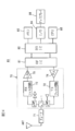
- FIG. 24 shows a front-end circuit (high-frequency circuit) 70 including the non-reciprocal circuit element (3-port pattern circulator, denoted by reference numeral 1) and a communication circuit (cellular phone) 80 including the circuit 70.
- the front end circuit 70 is obtained by inserting a circulator 1 ⁇ / b> A between a tuner 71 of the antenna ANT and a TX filter circuit 72 and an RX filter circuit 73.
- the filter circuits 72 and 73 are connected to the RFIC 81 via a power amplifier (power amplifier) 74 and a low noise amplifier 75, respectively.
- the front end circuit 70 may include an antenna ANT and a tuner 71.
- the communication device 80 includes an RFIC 81 and a BBIC 82 with respect to the front end circuit 70, a memory 83, an I / O 84, and a CPU 85 are connected to the BBIC 82, and a display 86 and the like are connected to the I / O 84.
- the nonreciprocal circuit element, the high frequency circuit, and the communication device according to the present invention are not limited to the above-described embodiments, and can be variously modified within the scope of the gist.
- the configuration, shape, number, etc. of the central conductor are arbitrary.
- the capacitive element or the like may be constituted by a conductor built in the circuit board in addition to being mounted on the circuit board as a chip type.
- the present invention is useful for non-reciprocal circuit devices, and is particularly excellent in that a decrease in magnetic efficiency can be suppressed while achieving a low profile.
- Non-reciprocal circuit element 10 Magnetic rotor 20 ... Ferrite 21, 22, 23 ... Center conductor 30, 31-34 ... Permanent magnet 41-46 ... External connection electrode 51 ... Top surface side yoke 52 ; Mounting surface side yoke 70 ... Front end circuit 80 ... Communication device
Landscapes
- Non-Reversible Transmitting Devices (AREA)
Abstract
非可逆回路素子において、低背化を達成するとともに、永久磁石による磁気効率の低下を極力抑制する。 フェライト(20)に複数の中心導体が配置されており、天面、実装面及び側面を有する磁気回転子(10)と、磁気回転子(10)の側面側に配置された永久磁石(30),(31)~(34)と、磁気回転子(10)の天面側及び実装面側にそれぞれ配置されたヨーク(51),(52)と、を備えた非可逆回路素子。天面側ヨーク(51)及び実装面側ヨーク(52)の少なくともいずれかのヨークの端部が、平面視で、永久磁石(31)~(34)と重なりかつ永久磁石(31)~(34)の端面よりも内側に存在している。
Description
本発明は、非可逆回路素子、特に、マイクロ波帯で使用されるサーキュレータやアイソレータなどの非可逆回路素子に関し、さらに該素子を備えた高周波回路及び通信装置に関する。
従来より、サーキュレータやアイソレータなどの非可逆回路素子は、予め定められた特定方向にのみ信号を伝送し、逆方向には伝送しない特性を有している。この特性を利用して、例えば、サーキュレータは、携帯電話などの移動体通信機器の送受信回路部に使用されている。
特許文献1には、複数のストリップラインを配置したフェライト板と、該フェライト板の側面の周囲に配置された複数個の磁石と、フェライト板を挟むように配置された2枚のヨーク板とを備えた非可逆回路素子が記載されている。この非可逆回路素子では、フェライト板の側面側に磁石を配置することで薄型(低背化)を達成している。同様の趣旨で、フェライトの側面側に磁石を配置した非可逆回路素子は、例えば特許文献2,3にも記載されている。
この種の非可逆回路素子の一般的な構造を図23(B)に示す。中心導体を含むフェライト120からなる磁気回転子110の側面側に永久磁石131,132が配置され、磁気回転子110の天面側及び実装面側にヨーク151,152が配置されている。しかしながら、この種の非可逆回路素子では、平面視で、ヨーク151,152の端部が永久磁石131,132の端面まで延在されているため、フェライト120を通過する磁束φ1以外に漏れ磁束φ2が発生し、永久磁石131,132による磁気効率が低下するという問題点を有していた。また、非可逆回路素子では小型化を達成することが重要な課題である。
本発明の目的は、低背化を達成するとともに、永久磁石による磁気効率の低下を極力抑制できる非可逆回路素子、高周波回路及び通信装置を提供することにある。
本発明の第1の形態である非可逆回路素子は、
フェライトに複数の中心導体が配置されており、天面、実装面及び側面を有する磁気回転子と、
前記磁気回転子の側面側に配置された永久磁石と、
前記磁気回転子の天面側及び実装面側にそれぞれ配置されたヨークと、
を備えた非可逆回路素子において、
前記天面側ヨーク及び前記実装面側ヨークの少なくともいずれかのヨークの端部が、平面視で、前記永久磁石と重なりかつ該永久磁石の端面よりも内側に存在すること、
を特徴とする。
フェライトに複数の中心導体が配置されており、天面、実装面及び側面を有する磁気回転子と、
前記磁気回転子の側面側に配置された永久磁石と、
前記磁気回転子の天面側及び実装面側にそれぞれ配置されたヨークと、
を備えた非可逆回路素子において、
前記天面側ヨーク及び前記実装面側ヨークの少なくともいずれかのヨークの端部が、平面視で、前記永久磁石と重なりかつ該永久磁石の端面よりも内側に存在すること、
を特徴とする。
本発明の第2の形態である高周波回路は、前記非可逆回路素子と電力増幅器とを含むこと、
を特徴とする。
を特徴とする。
本発明の第3の形態である通信装置は、前記非可逆回路素子とRFICとを含むこと、
を特徴とする。
を特徴とする。
前記非可逆回路素子にあっては、永久磁石が磁気回転子の側面側に配置されるために低背化が達成されるとともに、天面側ヨーク及び実装面側ヨークの少なくともいずれかのヨークの端部が、平面視で、永久磁石と重なりかつ該永久磁石の端面よりも内側に存在するため、漏れ磁束が少なくなり、磁気効率の低下が極力抑制される。
本発明によれば、非可逆回路素子の低背化を達成しつつ磁気効率の低下を抑制できる。
以下に、非可逆回路素子、高周波回路及び通信装置の実施例について添付図面を参照して説明する。なお、各図において同じ部材には共通する符号を付し、重複する説明は省略する。
(第1実施例、図1~図5参照)
第1実施例である非可逆回路素子1Aは、図1に示す等価回路を有する集中定数型の3ポート型サーキュレータである。即ち、永久磁石により矢印A方向に直流磁界が印加されるフェライト20に第1中心導体21(L1)、第2中心導体22(L2)及び第3中心導体23(L3)をそれぞれ絶縁状態で所定の角度で交差させて配置している。第1中心導体21の一端を第1ポートP1、第2中心導体22の一端を第2ポートP2、第3中心導体23の一端を第3ポートP3としている。各中心導体21,22,23のそれぞれの他端はグランドに接続されている。さらに、各中心導体21,22,23に対して容量素子C1,C2,C3がそれぞれ並列に接続されている。
第1実施例である非可逆回路素子1Aは、図1に示す等価回路を有する集中定数型の3ポート型サーキュレータである。即ち、永久磁石により矢印A方向に直流磁界が印加されるフェライト20に第1中心導体21(L1)、第2中心導体22(L2)及び第3中心導体23(L3)をそれぞれ絶縁状態で所定の角度で交差させて配置している。第1中心導体21の一端を第1ポートP1、第2中心導体22の一端を第2ポートP2、第3中心導体23の一端を第3ポートP3としている。各中心導体21,22,23のそれぞれの他端はグランドに接続されている。さらに、各中心導体21,22,23に対して容量素子C1,C2,C3がそれぞれ並列に接続されている。
ここで、第1中心導体21の一端を外部接続用電極41、他端を外部接続用電極42とし、第2中心導体22の一端を外部接続用電極43、他端を外部接続用電極44とし、第3中心電極23の一端を外部接続用電極45、他端を外部接続用電極46とする。また、この非可逆回路素子1が携帯電話などの送受信回路部に組み込まれる場合、第1ポートP1は送信側(TX)に接続され、第2ポートP2は受信側(RX)に接続され、第3ポートP3はアンテナ側(ANT)に接続される。
送受信回路部における非可逆回路素子1A(3ポート型サーキュレータ)の動作は以下のとおりである。即ち、第1ポートP1(送信回路TX)から入力された高周波信号は、第3ポートP3(アンテナANT)から出力され、第3ポートP3(アンテナANT)から入力された高周波信号は第2ポートP2(受信回路RX)に入力される。第2ポートP2の高周波信号は送受信回路部で減衰されて第1ポートP1に伝達されることはない。
非可逆回路素子1Aは、具体的には、図2に示す磁気回転子10にて構成されている。この磁気回転子10は、矩形状のマイクロ波フェライト20の天面側及び実装面側にガラスを主成分とする絶縁体層11,12,13,14や各種導体、各種電極を積層したもので、フェライト20にも天面側及び実装面側に設けた各種導体をコイル状に接続するための複数のスルーホール導体や複数の電極が形成されている。
詳しくは、第1中心導体21(L1)を形成する導体21a,21b,21cは絶縁体層12上に形成され、導体21d,21eは絶縁体層13とフェライト20の間に形成されている。導体21aの端部は外部引出し部41aとされ、導体21cの端部は外部引出し部42aとされている。導体21aの他端は導体21fを介して導体21dの一端に接続され、該導体21dの他端は導体21gを介して導体21bの一端に接続されている。該導体21bの他端は導体21hを介して導体21eの一端に接続され、該導体21eの他端は導体21iを介して導体21cの一端に接続されている。
第2中心導体22(L2)を形成する導体22a,22b,22cは絶縁体層11とフェライト20の間に形成され、導体22d,22eは絶縁体層14の下面に形成されている。導体22aの端部は外部引出し部43aとされ、導体22cの端部は外部引出し部44aとされている。導体22aの他端は導体22fを介して導体22dの一端に接続され、該導体22dの他端は導体22gを介して導体22bの一端に接続されている。該導体22bの他端は導体22hを介して導体22eの一端に接続され、該導体22eの他端は導体22iを介して導体22cの一端に接続されている。
第3中心導体23(L3)を形成する導体23a,23b,23cは絶縁体層11,12の間に形成され、導体23d,23eは絶縁体層13,14の間に形成されている。導体23aの端部は外部引出し部46aとされ、導体23cの端部は外部引出し部45aとされている。導体23aの他端は導体23fを介して導体23dの一端に接続され、該導体23dの他端は導体23gを介して導体23bの一端に接続されている。該導体23bの他端は導体23hを介して導体23eの一端に接続され、該導体23eの他端は導体23iを介して導体23cの一端に接続されている。
外部接続用電極41は導体21aの端部である外部引出し部41aとそれに接続されている電極によって形成されている。外部接続用電極42は導体21cの端部である外部引出し部42aとそれに接続されている電極によって形成されている。外部接続用電極43は導体22aの端部である外部引出し部43aとそれに接続されている電極によって形成されている。外部接続用電極44は導体22cの端部である外部引出し部44aとそれに接続されている電極によって形成されている。外部接続用電極45は導体23cの端部である外部引出し部45aとそれに接続されている電極によって形成されている。外部接続用電極46は導体23aの端部である外部引出し部46aとそれに接続されている電極によって形成されている。
中心導体21,22,23は、Ag,Cuなどの薄膜導体、厚膜導体又は導体箔として形成することができ、感光性の金属ペーストを使用することが好ましい。絶縁体層11~14は感光性ガラス、ポリイミドなど絶縁抵抗の高い材料を使用することが好ましい。導体層や絶縁層はフォトリソグラフィやエッチング、印刷などで形成できる。外部接続用電極41~46やスルーホール用導体は、好ましくは、Ag,Cuを主成分とする導電性の電極材料(ペースト)を塗布して焼き付け、その表面にNiのめっき層を形成し、さらに、Au,Sn,Ag,Cuなどのめっき層を形成する。めっきに限定するものではなく、スパッタ処理などであってもよい。一方、容量素子C1,C2,C3はチップ部品を使用する。
以上の構成からなる磁気回転子10は、図3に示すように、四つの側面側に永久磁石31~34が配置され、天面側にヨーク51が配置されるとともに実装面側にヨーク52が配置されることで非可逆回路素子1Aとされる。ヨーク51,52は、SPCCなどの磁性体を素材とすることが望ましく、Fe,Ni,Coの単体金属あるいはこれらを主成分とする合金であってもよい。ヨーク51,52の表面には高周波損を低減するためにAgやAuのめっき層を形成してもよい。磁気回転子10や永久磁石31~34はヨーク51,52に挟まれた状態で図示しない樹脂を接着剤として一体化される。つまり、図3(A)に示されている空隙部分は樹脂にて充填される。このように、磁気回転子10の側面側に永久磁石31~34を配置し、上下面をヨーク51,52で挟み込んだ構造体を、本明細書においてはフェライト・磁石組立体と称する。
ところで、実装面側のヨーク52は、図3(C)に示すように、複数のセグメント52a,52b,52c,52dに分割されており、電極41(第1ポートP1、TX)はセグメント52aに接続され、電極43(第2ポートP2、RX)はセグメント52bに接続され、電極45(第3ポートP3、ANT)はセグメント52cに接続される。また、電極42,44,46(GND)はセグメント52dに接続される。即ち、磁気回転子10の電極41~46は、それぞれ電気的に絶縁状態で分割されたセグメント52a,52b,52c,52dを介して送信回路、受信回路、アンテナなどに接続される。
さらに、本第1実施例において重要な点は、ヨーク51,52の端部が平面視で永久磁石31~34と重なりかつ永久磁石31~34の端面よりも内側に存在することである。それゆえ、図23(A)に示すように、ヨーク51,52の端部から外部に漏れる磁束(図23(B)の従来例で示す漏れ磁束φ2)がほとんどなくなり、ほとんどの磁束がフェライト20を通過することになり(磁束φ1)、磁気効率が向上する。
具体的な磁気特性を図4及び図5に示す。図4はフェライト20を通過する磁束密度(丸印で示す、左縦軸参照、以下、有効磁束密度と記す)と漏れ磁束(三角印で示す、右縦軸参照)とを、磁石31~34に対するヨーク51,52の寸法差(両側での寸法差として示す、片側ではその半分の数値である)に基づいて示している。即ち、ヨーク51(52)の端部間距離をCとし、一対の永久磁石31,32(33,34)の端面間距離をDとするとき、その差(C-D)を横軸としている。図4によると、寸法差0mmとは図23(B)に示す従来例であり、そのときのフェライト20を通過する磁束密度は約115mTであり、漏れ磁束は約30mTである。有効磁束密度は寸法差(C-D)が-0.2mm(片側では-0.1mm)で極大値をとり、該極大値は磁束密度の変化が小さい領域であり、量産品でのロバスト性が高い。一方、漏れ磁束は寸法差(C-D)が-0.2mm(片側では-0.1mm)で極小値をとり、該極小値では周辺回路素子への磁気的影響が少ないので高密度実装に寄与する。
図4から明らかなように、寸法差(C-D)が0mmから-0.4mmの間は有効磁束密度が約115mTよりも大きく、漏れ磁束が約30mTよりも小さい。それゆえ、-0.4mm<(C-D)<0mmであることが好ましい。
図5は有効磁束密度(丸印で示す、左縦軸参照)と漏れ磁束(三角印で示す、右縦軸参照)とを、ヨーク51,52と永久磁石31~34との寸法比に基づいて示している。即ち、永久磁石31~34の幅寸法をBとし、ヨーク51,52の端部が永久磁石31~34と重なる幅寸法をAとするとき、寸法比(A/B)を横軸としている。図5によると、寸法比1.0とは図23(B)に示す従来例であり、そのときのフェライト20を通過する磁束密度は約115mTであり、漏れ磁束は約30mTである。有効磁束密度は寸法比が約0.7で極大値をとり、該極大値は磁束密度の変化が小さい領域であり、量産品でのロバスト性が高い。一方、漏れ磁束は寸法比が約0.7で極小値をとり、該極小値では周辺回路素子への磁気的影響が少ないので高密度実装に寄与する。
図5から明らかなように、寸法比(A/B)が0.4から1.0の間は有効磁束密度が約115mTよりも大きく、漏れ磁束が約30mTよりも小さい。それゆえ、0.4<(A/B)<1.0であることが好ましい。
ちなみに、図4及び図5のデータをシミュレートしたときの磁気回転子10において、永久磁石31,32のサイズは、幅0.35mm、長さ2.2mm、高さ0.48mmであった。永久磁石33,34のサイズは、幅0.35mm、長さ1.2mm、高さ0.48mmであった。ヨーク51,52の外形サイズは、短辺が1.8mm、長辺が2.00mmであった。漏れ磁束は永久磁石31~34の端面から2mm離れた箇所での値である。
前記磁気回転子10は必ずしも平面視で4角形である必要はない。また、永久磁石とヨークは様々な配置関係をとることができる。その第1例は、第1実施例として示したように、磁気回転子10の四つの側面側にそれぞれ永久磁石31~34を一つずつ配置し、ヨーク51,52の端部が4辺全てで永久磁石31~34の端面よりも内側に位置させたものである。永久磁石は少なくとも一対のものが配置されていればよく、また、ヨーク51,52のいずれかの端部が永久磁石の端面よりも内側に存在していればよい。以下に、この配置関係の様々な例を示す。
(永久磁石とヨークとの種々の配置関係、図6~図11参照)
図6は第2例を示し、天面側のヨーク51は1辺においてその端部が永久磁石33,31,32の端面よりも内側に存在しており、他の3辺においてその端部が永久磁石34,31,32の端面と等しい。実装面側のヨーク52は4辺においてその端部が永久磁石31~34の端面と等しい。
図6は第2例を示し、天面側のヨーク51は1辺においてその端部が永久磁石33,31,32の端面よりも内側に存在しており、他の3辺においてその端部が永久磁石34,31,32の端面と等しい。実装面側のヨーク52は4辺においてその端部が永久磁石31~34の端面と等しい。
図7は第3例を示し、天面側のヨーク51は2辺においてその端部が永久磁石31~34の端面よりも内側に存在しており、他の2辺はその端部が永久磁石31,32の端面と等しい。実装面側のヨーク52は4辺においてその端部が永久磁石31~34の端面と等しい。
図8は第4例を示し、天面側のヨーク51は2辺においてその端部が永久磁石31~34の端面よりも内側に存在しており、他の2辺はその端部が永久磁石31,32の端面と等しい。実装面側のヨーク52は1辺においてその端部が永久磁石33,31,32の端面よりも内側に存在しており、他の3辺においてその端部が永久磁石34,31,32の端面と等しい。
図9は第5例を示し、天面側のヨーク51は1辺においてその端部が永久磁石33,31,32の端面よりも内側に存在しており、他の3辺においてその端部が永久磁石34,31,32の端面と等しい。実装面側のヨーク52は1辺においてその端部が永久磁石33,31,32の端面よりも内側に存在しており、他の3辺においてその端部が永久磁石34,31,32の端面と等しい。
図10は第6例を示し、天面側のヨーク51は1辺においてその端部が永久磁石33,31,32の端面よりも内側に存在しており、他の3辺においてその端部が永久磁石34,31,32の端面と等しい。実装面側のヨーク52は2辺においてその端部が永久磁石31~34の端面よりも内側に存在しており、他の2辺はその端部が永久磁石31,32の端面と等しい。
図11は第7例を示し、天面側のヨーク51は2辺においてその端部が永久磁石31~34の端面よりも内側に存在しており、他の2辺はその端部が永久磁石31,32の端面と等しい。実装面側のヨーク52は2辺においてその端部が永久磁石31~34の端面よりも内側に存在しており、他の2辺はその端部が永久磁石31,32の端面と等しい。
(製造例、図12及び図13参照)
前記非可逆回路素子1Aの製造において、フェライト・磁石組立体は、図12及び図13に示す広い面積のヨーク(集合基板51A,52A)の間に、磁気回転子10と永久磁石31~34をマトリクス状に配置し、1単位の素子1Aとなるように切り出す。この場合、集合基板51A,52Aには個々のヨーク51,52の端部が永久磁石31~34の端面よりも内側に配置されるように、縦横方向にそれぞれスリット53a,54aが形成される。同時に、1単位のヨーク51,52が分離しないように、スリット53a,54aにブリッジ53b,54bを設けておく。
前記非可逆回路素子1Aの製造において、フェライト・磁石組立体は、図12及び図13に示す広い面積のヨーク(集合基板51A,52A)の間に、磁気回転子10と永久磁石31~34をマトリクス状に配置し、1単位の素子1Aとなるように切り出す。この場合、集合基板51A,52Aには個々のヨーク51,52の端部が永久磁石31~34の端面よりも内側に配置されるように、縦横方向にそれぞれスリット53a,54aが形成される。同時に、1単位のヨーク51,52が分離しないように、スリット53a,54aにブリッジ53b,54bを設けておく。
集合状態のフェライト・磁石組立体は、集合基板51A,52Aの間に比透磁率が約1.0の樹脂材55(図14参照)が充填されて一体化され、集合基板51A,52Aを図12及び図13に示す一点鎖線X,Yでカットすることにより、1単位の素子1Aとして切り出される。樹脂材55を充填することにより、フェライト・磁石組立体が一体化されるとともに、樹脂材55が永久磁石31~34の角部にも行きわたり永久磁石31~34の欠けや割れが未然に防止される。比透磁率が1.0の樹脂材55を用いることで、漏れ磁束が増加することはない。
また、磁気回転子10の各種電極は実装面側のヨーク52の各セグメント52a,52b,52c,52dにはんだ56(図14参照)を介して電気的に接続される。
(第2実施例、図15~図17参照)
第2実施例である非可逆回路素子1Bは、前記第1実施例と同様に図1に示した等価回路を有する集中定数型の3ポート型サーキュレータであり、第1実施例である非可逆回路素子1Aとは、実装面側のヨーク52(図15(C)参照)がセグメントに分割されておらず1枚もので形成されている点で異なり、他の構成は同じである。
第2実施例である非可逆回路素子1Bは、前記第1実施例と同様に図1に示した等価回路を有する集中定数型の3ポート型サーキュレータであり、第1実施例である非可逆回路素子1Aとは、実装面側のヨーク52(図15(C)参照)がセグメントに分割されておらず1枚もので形成されている点で異なり、他の構成は同じである。
この非可逆回路素子1Bにおいて、磁気回転子10に形成された各種電極41~46は、実装面側のヨーク52に接続されることなく(ヨーク52とは樹脂材などで絶縁され)、磁気回転子10の側面から図示しない端子に電気的に接続され、それらの端子を介して送信回路、受信回路、アンテナなどに接続される。
本第2実施例においても、ヨーク51,52の端部が平面視で永久磁石31~34と重なりかつ永久磁石31~34の端面よりも内側に存在する(図15(B),(C))。それゆえ、ヨーク51,52の端部から外部に漏れる磁束がほとんどなくなり、ほとんどの磁束がフェライト20を通過することになり、磁気効率が向上する。また、ヨーク51,52の端部と永久磁石31~34の端面との関係も、例えば図6~図11に示した種々の配置関係を採用することができる。
本第2実施例にあっては、実装面側のヨーク52が1枚ものである(分割されていない)点で、第1実施例よりも磁気特性は良好である。その磁気特性を図16及び図17に示す。図16は、図4に対応し、フェライト20を通過する磁束密度(丸印で示す、左縦軸参照、以下、有効磁束密度と記す)と漏れ磁束(三角印で示す、右縦軸参照)とを、磁石31~34に対するヨーク51,52の寸法差(両側での寸法差として示す、片側ではその半分の数値である)に基づいて示している。即ち、ヨーク51(52)の端部間距離をCとし、一対の永久磁石31,32(33,34)の端面間距離をDとするとき、その差(C-D)を横軸としている。図16によると、寸法差0mmとは図23(B)に示す従来例であり、そのときのフェライト20を通過する磁束密度は約120mTであり、漏れ磁束は約28mTである。有効磁束密度は寸法差(C-D)が-0.2mm(片側では-0.1mm)で極大値をとり、該極大値は磁束密度の変化が小さい領域であり、量産品でのロバスト性が高い。一方、漏れ磁束は寸法差(C-D)が-0.2mm(片側では-0.1mm)で極小値をとり、該極小値では周辺回路素子への磁気的影響が少ないので高密度実装に寄与する。
図16から明らかなように、寸法差(C-D)が0mmから-0.4mmの間は有効磁束密度が約120mTよりも大きく、漏れ磁束が約28mTよりも小さい。それゆえ、-0.4mm<(C-D)<0mmであることが好ましい。
図17は有効磁束密度(丸印で示す、左縦軸参照)と漏れ磁束(三角印で示す、右縦軸参照)とを、ヨーク51,52と永久磁石31~34との寸法比に基づいて示している。即ち、永久磁石31~34の幅寸法をBとし、ヨーク51,52の端部が永久磁石31~34と重なる幅寸法をAとするとき、寸法比(A/B)を横軸としている。図17によると、寸法比1.0とは図23(B)に示す従来例であり、そのときのフェライト20を通過する磁束密度は約120mTであり、漏れ磁束は約28mTである。有効磁束密度は寸法比が約0.7で極大値をとり、該極大値は磁束密度の変化が小さい領域であり、量産品でのロバスト性が高い。一方、漏れ磁束は寸法比が約0.7で極小値をとり、該極小値では周辺回路素子への磁気的影響が少ないので高密度実装に寄与する。
図17から明らかなように、寸法比(A/B)が0.4から1.0の間は有効磁束密度が約120mTよりも大きく、漏れ磁束が約28mTよりも小さい。それゆえ、0.4<(A/B)<1.0であることが好ましい。
ちなみに、図16及び図17のデータをシミュレートしたときの磁気回転子10において、永久磁石31,32のサイズは、幅0.35mm、長さ2.2mm、高さ0.48mmであった。永久磁石33,34のサイズは、幅0.35mm、長さ1.2mm、高さ0.48mmであった。ヨーク51,52の外形サイズは、短辺が1.8mm、長辺が2.00mmであった。漏れ磁束は永久磁石31~34の端面から2mm離れた箇所での値である。
(製造例、図18及び図19参照)
前記非可逆回路素子1Bの製造においても、フェライト・磁石組立体は、図18に示す広い面積のヨーク(集合基板51A,52A)の間に、磁気回転子10と永久磁石31~34をマトリクス状に配置し、1単位の素子1Bとなるように切り出す。この場合、集合基板51A,52Aには個々のヨーク51,52の端部が永久磁石31~34の端面よりも内側に配置されるように、縦横方向にそれぞれスリット53a,54aが形成される。同時に、1単位のヨーク51,52が分離しないように、スリット53a,54aにブリッジ53b,53bを設けておく。集合状態のフェライト・磁石組立体は、集合基板51A,52Aの間に図14に示した樹脂材55が充填されて一体化されており、集合基板51A,52Aを図18に示す一点鎖線X,Yでカットすることにより、1単位の素子1Bとして切り出される。
前記非可逆回路素子1Bの製造においても、フェライト・磁石組立体は、図18に示す広い面積のヨーク(集合基板51A,52A)の間に、磁気回転子10と永久磁石31~34をマトリクス状に配置し、1単位の素子1Bとなるように切り出す。この場合、集合基板51A,52Aには個々のヨーク51,52の端部が永久磁石31~34の端面よりも内側に配置されるように、縦横方向にそれぞれスリット53a,54aが形成される。同時に、1単位のヨーク51,52が分離しないように、スリット53a,54aにブリッジ53b,53bを設けておく。集合状態のフェライト・磁石組立体は、集合基板51A,52Aの間に図14に示した樹脂材55が充填されて一体化されており、集合基板51A,52Aを図18に示す一点鎖線X,Yでカットすることにより、1単位の素子1Bとして切り出される。
また、製造時におけるヨーク51,52の分離を避けるためには、図19に示すように、個別に分離されたヨーク51,52をシート57に貼着した状態とし、これを集合基板として用いてもよい。この場合においても、シート57を一点鎖線X,Yでカットすることにより、1単位の素子1Bとして切り出すことができる。
(第3実施例、図20及び図21参照)
第3実施例である非可逆回路素子1Cは、前記第1実施例と同様に図1に示した等価回路を有する集中定数型の3ポート型サーキュレータであり、図20に示すように、天面側のヨーク51及び実装面側のヨーク52にあっては、それらの端部が平面視で永久磁石31~34の端面と等しい。つまり、本第3実施例は、前記第1実施例との対比でいえば、実装面側のヨーク52がセグメント52a~52dに分割されている点で同じであるが、ヨーク51,52がともにそれらの端部が平面視で永久磁石31~34の端面と等しい点で相違している。
第3実施例である非可逆回路素子1Cは、前記第1実施例と同様に図1に示した等価回路を有する集中定数型の3ポート型サーキュレータであり、図20に示すように、天面側のヨーク51及び実装面側のヨーク52にあっては、それらの端部が平面視で永久磁石31~34の端面と等しい。つまり、本第3実施例は、前記第1実施例との対比でいえば、実装面側のヨーク52がセグメント52a~52dに分割されている点で同じであるが、ヨーク51,52がともにそれらの端部が平面視で永久磁石31~34の端面と等しい点で相違している。
即ち、この非可逆回路素子1Cは、
フェライトに複数の中心導体が配置されており、天面、実装面及び側面を有する磁気回転子と、
前記磁気回転子の側面側に配置された永久磁石と、
前記磁気回転子の天面側及び実装面側にそれぞれ配置されたヨークと、
を備えた非可逆回路素子において、
前記磁気回転素子には前記実装面側に前記複数の中心導体と接続された電極が形成されており、
前記実装面側のヨークは前記電極のそれぞれと接続された複数のセグメントに分割されていること、
を特徴とする。
フェライトに複数の中心導体が配置されており、天面、実装面及び側面を有する磁気回転子と、
前記磁気回転子の側面側に配置された永久磁石と、
前記磁気回転子の天面側及び実装面側にそれぞれ配置されたヨークと、
を備えた非可逆回路素子において、
前記磁気回転素子には前記実装面側に前記複数の中心導体と接続された電極が形成されており、
前記実装面側のヨークは前記電極のそれぞれと接続された複数のセグメントに分割されていること、
を特徴とする。
前記電極は少なくとも四つの送信端子、受信端子、アンテナ端子及びグランド端子であり、前記ヨークの分割された複数のセグメントは前記送信端子、受信端子、アンテナ端子及びグランド端子と接続されている。
この第3実施例においては、実装面側のヨーク52を複数のセグメントに分割し、磁気回転子10の接続用端子として機能させることで、フェライト・磁石組立体に接続端子を設ける必要がなくなり、非可逆回路素子の小型化に繋がる。なお、ヨーク51,52の端部は永久磁石31~34の端面よりも平面視で外側又は内側のいずれに存在していてもよい。
本第3実施例である非可逆回路素子1Cの製造においては、図21に示すように、実装面側のヨーク52となるべき集合基板52Aにはセグメント52a~52dを設けるためのスリット54aが形成されている。一方、天面側のヨーク51は広い面積の1枚の(スリットのない)集合基板である。これらの集合基板の間に磁気回転子10をマトリクス状に配置し、一点鎖線X,Yでカットし、1単位の素子1Cとして切り出す。
(第4実施例、図22参照)
第4実施例である非可逆回路素子1Dは、前記第1実施例と同様に図1に示した等価回路を有する集中定数型の3ポート型サーキュレータであり、図22に示すように、ロ字型の永久磁石30を磁気回転子10の側部に配置し、天面側及び実装面側にそれぞれヨーク51,52を配置したものである。本第4実施例での作用効果は前記第1実施例と基本的に同様である。
第4実施例である非可逆回路素子1Dは、前記第1実施例と同様に図1に示した等価回路を有する集中定数型の3ポート型サーキュレータであり、図22に示すように、ロ字型の永久磁石30を磁気回転子10の側部に配置し、天面側及び実装面側にそれぞれヨーク51,52を配置したものである。本第4実施例での作用効果は前記第1実施例と基本的に同様である。
(通信装置、図24参照)
次に、通信装置について説明する。図24に前記非可逆回路素子(3ポート柄サーキュレータ、符号1で示す)を含むフロントエンド回路(高周波回路)70及び該回路70を含む通信回路(携帯電話)80を示す。フロントエンド回路70はアンテナANTのチューナ71及びTXフィルタ回路72とRXフィルタ回路73との間にサーキュレータ1Aを挿入したものである。フィルタ回路72,73はそれぞれパワーアンプ(電力増幅器)74、ローノイズアンプ75を介してRFIC81に接続されている。なお、フロントエンド回路70としてはアンテナANT及びチューナ71を含む場合もあり得る。
次に、通信装置について説明する。図24に前記非可逆回路素子(3ポート柄サーキュレータ、符号1で示す)を含むフロントエンド回路(高周波回路)70及び該回路70を含む通信回路(携帯電話)80を示す。フロントエンド回路70はアンテナANTのチューナ71及びTXフィルタ回路72とRXフィルタ回路73との間にサーキュレータ1Aを挿入したものである。フィルタ回路72,73はそれぞれパワーアンプ(電力増幅器)74、ローノイズアンプ75を介してRFIC81に接続されている。なお、フロントエンド回路70としてはアンテナANT及びチューナ71を含む場合もあり得る。
通信装置80は前記フロントエンド回路70に対して、RFIC81、BBIC82を備え、BBIC82にはメモリ83、I/O84、CPU85が接続され、I/O84にはディスプレイ86などが接続されている。
(他の実施例)
なお、本発明に係る非可逆回路素子、高周波回路及び通信装置は、前記実施例に限定されるものではなく、その要旨の範囲内で種々に変更することができる。
なお、本発明に係る非可逆回路素子、高周波回路及び通信装置は、前記実施例に限定されるものではなく、その要旨の範囲内で種々に変更することができる。
例えば、中心導体の構成や形状、本数などは任意である。また、容量素子などは、チップタイプとして回路基板上に実装する以外に、回路基板に内蔵した導体で構成してもよい。
以上のように、本発明は、非可逆回路素子に有用であり、特に、低背化を達成しつつ磁気効率の低下を抑制できる点で優れている。
1A,1B,1C,1D…非可逆回路素子
10…磁気回転子
20…フェライト
21,22,23…中心導体
30,31~34…永久磁石
41~46…外部接続電極
51…天面側ヨーク
52…実装面側ヨーク
70…フロンドエンド回路
80…通信装置
10…磁気回転子
20…フェライト
21,22,23…中心導体
30,31~34…永久磁石
41~46…外部接続電極
51…天面側ヨーク
52…実装面側ヨーク
70…フロンドエンド回路
80…通信装置
Claims (9)
- フェライトに複数の中心導体が配置されており、天面、実装面及び側面を有する磁気回転子と、
前記磁気回転子の側面側に配置された永久磁石と、
前記磁気回転子の天面側及び実装面側にそれぞれ配置されたヨークと、
を備えた非可逆回路素子において、
前記天面側ヨーク及び前記実装面側ヨークの少なくともいずれかのヨークの端部が、平面視で、前記永久磁石と重なりかつ該永久磁石の端面よりも内側に存在すること、
を特徴とする非可逆回路素子。 - 平面視での、前記永久磁石の幅寸法をBとし、前記ヨークの端部が該永久磁石と重なる幅寸法をAとするとき、0.4<(A/B)<1.0であること、
を特徴とする請求項1に記載の非可逆回路素子。 - 平面視での、前記ヨークの端部間距離をCとし、一対の前記永久磁石の端面間距離をDとするとき、-0.4mm<(C-D)<0mmであること、
を特徴とする請求項1に記載の非可逆回路素子。 - 前記永久磁石の天面側及び実装面側の少なくともいずれかの端部であって前記ヨークと重なっていない部分に、比透磁率が約1.0の樹脂が配置されていること、
を特徴とする請求項1ないし請求項3のいずれかに記載の非可逆回路素子。 - 前記磁気回転子、前記永久磁石及び前記ヨークは比透磁率が約1.0の樹脂にて接着されていること、
を特徴とする請求項1ないし請求項3のいずれかに記載の非可逆回路素子。 - 前記磁気回転子には前記実装面側に前記複数の中心導体と接続された電極が形成されており、
前記実装面側のヨークは前記電極のそれぞれと接続された複数のセグメントに分割されていること、
を特徴とする請求項1ないし請求項5のいずれかに記載の非可逆回路素子。 - 前記電極は少なくとも四つの送信端子、受信端子、アンテナ端子及びグランド端子であり、
前記ヨークの分割された複数のセグメントは前記送信端子、前記受信端子、前記アンテナ端子及び前記グランド端子と接続されていること、
を特徴とする請求項6に記載の非可逆回路素子。 - 請求項1ないし請求項7のいずれかに記載の非可逆回路素子と電力増幅器とを含むこと、
を特徴とする高周波回路。 - 請求項1ないし請求項7のいずれかに記載の非可逆回路素子とRFICとを含むこと、
を特徴とする通信装置。
Priority Applications (1)
| Application Number | Priority Date | Filing Date | Title |
|---|---|---|---|
| US15/850,339 US20180115038A1 (en) | 2015-06-25 | 2017-12-21 | Non-reciprocal circuit element, high-frequency circuit and communication device |
Applications Claiming Priority (2)
| Application Number | Priority Date | Filing Date | Title |
|---|---|---|---|
| JP2015127580 | 2015-06-25 | ||
| JP2015-127580 | 2015-06-25 |
Related Child Applications (1)
| Application Number | Title | Priority Date | Filing Date |
|---|---|---|---|
| US15/850,339 Continuation US20180115038A1 (en) | 2015-06-25 | 2017-12-21 | Non-reciprocal circuit element, high-frequency circuit and communication device |
Publications (1)
| Publication Number | Publication Date |
|---|---|
| WO2016208643A1 true WO2016208643A1 (ja) | 2016-12-29 |
Family
ID=57585002
Family Applications (1)
| Application Number | Title | Priority Date | Filing Date |
|---|---|---|---|
| PCT/JP2016/068578 Ceased WO2016208643A1 (ja) | 2015-06-25 | 2016-06-22 | 非可逆回路素子、高周波回路及び通信装置 |
Country Status (2)
| Country | Link |
|---|---|
| US (1) | US20180115038A1 (ja) |
| WO (1) | WO2016208643A1 (ja) |
Citations (2)
| Publication number | Priority date | Publication date | Assignee | Title |
|---|---|---|---|---|
| JP2012119801A (ja) * | 2010-11-30 | 2012-06-21 | Murata Mfg Co Ltd | 非可逆回路素子の製造方法 |
| JP2012257161A (ja) * | 2011-06-10 | 2012-12-27 | Murata Mfg Co Ltd | 電子部品モジュール |
-
2016
- 2016-06-22 WO PCT/JP2016/068578 patent/WO2016208643A1/ja not_active Ceased
-
2017
- 2017-12-21 US US15/850,339 patent/US20180115038A1/en not_active Abandoned
Patent Citations (2)
| Publication number | Priority date | Publication date | Assignee | Title |
|---|---|---|---|---|
| JP2012119801A (ja) * | 2010-11-30 | 2012-06-21 | Murata Mfg Co Ltd | 非可逆回路素子の製造方法 |
| JP2012257161A (ja) * | 2011-06-10 | 2012-12-27 | Murata Mfg Co Ltd | 電子部品モジュール |
Also Published As
| Publication number | Publication date |
|---|---|
| US20180115038A1 (en) | 2018-04-26 |
Similar Documents
| Publication | Publication Date | Title |
|---|---|---|
| JP5176989B2 (ja) | コモンモードフィルタ及びその実装構造 | |
| JPH11355012A (ja) | 非可逆回路素子 | |
| JP5843007B2 (ja) | 非可逆回路素子 | |
| JP6485430B2 (ja) | 非可逆回路素子及びこれを用いた通信装置 | |
| EP1970991A1 (en) | Non-reversible circuit element | |
| JP4665786B2 (ja) | 非可逆回路素子及び通信装置 | |
| WO2016208643A1 (ja) | 非可逆回路素子、高周波回路及び通信装置 | |
| JP6249104B2 (ja) | 非可逆回路素子 | |
| WO2015072252A1 (ja) | 非可逆回路素子 | |
| JP3939622B2 (ja) | 非可逆回路素子及びアイソレータ並びに非可逆回路素子の製造方法 | |
| JP4915366B2 (ja) | 非可逆回路素子 | |
| WO2014196324A1 (ja) | 非可逆回路素子 | |
| JP5136322B2 (ja) | 非可逆回路素子 | |
| JP4530165B2 (ja) | 非可逆回路素子及び通信装置 | |
| WO2017094407A1 (ja) | 非可逆回路素子、モジュール回路及び通信装置 | |
| JP2019134337A (ja) | 非可逆回路素子および高周波フロントエンド回路モジュール | |
| WO2017056689A1 (ja) | 非可逆回路素子、フロントエンド回路及び通信装置 | |
| JP5799830B2 (ja) | 非可逆回路素子 | |
| WO2017090304A1 (ja) | 非可逆回路素子、フロントエンド回路及び通信装置 | |
| JP2012235418A (ja) | 非可逆回路素子 | |
| JP4807457B2 (ja) | 非可逆回路素子 | |
| JP5413509B2 (ja) | アイソレータ | |
| JP2010081394A (ja) | 非可逆回路素子及びその製造方法 | |
| JP5652116B2 (ja) | 非可逆回路素子 | |
| JP2012138719A (ja) | 非可逆回路素子及びフェライト・磁石素子 |
Legal Events
| Date | Code | Title | Description |
|---|---|---|---|
| 121 | Ep: the epo has been informed by wipo that ep was designated in this application |
Ref document number: 16814413 Country of ref document: EP Kind code of ref document: A1 |
|
| NENP | Non-entry into the national phase |
Ref country code: DE |
|
| 122 | Ep: pct application non-entry in european phase |
Ref document number: 16814413 Country of ref document: EP Kind code of ref document: A1 |
|
| NENP | Non-entry into the national phase |
Ref country code: JP |