WO2016203976A1 - Esd保護装置 - Google Patents
Esd保護装置 Download PDFInfo
- Publication number
- WO2016203976A1 WO2016203976A1 PCT/JP2016/066430 JP2016066430W WO2016203976A1 WO 2016203976 A1 WO2016203976 A1 WO 2016203976A1 JP 2016066430 W JP2016066430 W JP 2016066430W WO 2016203976 A1 WO2016203976 A1 WO 2016203976A1
- Authority
- WO
- WIPO (PCT)
- Prior art keywords
- electrode
- discharge
- discharge electrode
- electrode portion
- counter
- Prior art date
- Legal status (The legal status is an assumption and is not a legal conclusion. Google has not performed a legal analysis and makes no representation as to the accuracy of the status listed.)
- Ceased
Links
Images




Classifications
-
- H—ELECTRICITY
- H01—ELECTRIC ELEMENTS
- H01T—SPARK GAPS; OVERVOLTAGE ARRESTERS USING SPARK GAPS; SPARKING PLUGS; CORONA DEVICES; GENERATING IONS TO BE INTRODUCED INTO NON-ENCLOSED GASES
- H01T1/00—Details of spark gaps
- H01T1/20—Means for starting arc or facilitating ignition of spark gap
-
- H—ELECTRICITY
- H01—ELECTRIC ELEMENTS
- H01T—SPARK GAPS; OVERVOLTAGE ARRESTERS USING SPARK GAPS; SPARKING PLUGS; CORONA DEVICES; GENERATING IONS TO BE INTRODUCED INTO NON-ENCLOSED GASES
- H01T4/00—Overvoltage arresters using spark gaps
- H01T4/10—Overvoltage arresters using spark gaps having a single gap or a plurality of gaps in parallel
-
- H—ELECTRICITY
- H01—ELECTRIC ELEMENTS
- H01T—SPARK GAPS; OVERVOLTAGE ARRESTERS USING SPARK GAPS; SPARKING PLUGS; CORONA DEVICES; GENERATING IONS TO BE INTRODUCED INTO NON-ENCLOSED GASES
- H01T4/00—Overvoltage arresters using spark gaps
- H01T4/10—Overvoltage arresters using spark gaps having a single gap or a plurality of gaps in parallel
- H01T4/12—Overvoltage arresters using spark gaps having a single gap or a plurality of gaps in parallel hermetically sealed
Definitions
- the present invention relates to an ESD protection device.
- the ESD protection device is provided between the first discharge electrode and the second discharge electrode, the first discharge electrode and the second discharge electrode that are provided on the element body, and are disposed to face each other.
- a discharge auxiliary electrode electrically connecting the discharge electrode and the second discharge electrode;
- the auxiliary discharge electrode extends in the opposing direction of the first discharge electrode and the second discharge electrode.
- the inventor of the present application has found that the conventional ESD protection device has a problem that resistance to ESD application is low by actually using the conventional ESD protection device. And this inventor earnestly examined this phenomenon and found the following causes.
- the coefficient of thermal expansion of the discharge auxiliary electrode is different from the coefficient of thermal expansion of the first discharge electrode, so that the discharge auxiliary electrode contacts the first discharge electrode. Thermal stress is generated on the surface. Due to this thermal stress, peeling (delamination) occurs between the auxiliary discharge electrode and the first discharge electrode. This peeling reduces the resistance to ESD application.
- an object of the present invention is to provide an ESD protection device with improved resistance to ESD application.
- the ESD protection apparatus of the present invention is With the body, A first discharge electrode and a second discharge electrode provided on the element body and arranged to face each other; A discharge auxiliary electrode provided between the first discharge electrode and the second discharge electrode and electrically connecting the first discharge electrode and the second discharge electrode;
- the discharge auxiliary electrode is A first surface direction electrode portion connected to the first discharge electrode and extending in a surface direction of the first discharge electrode; An opposing direction electrode portion connected to the first surface direction electrode portion and extending in an opposing direction of the first discharge electrode and the second discharge electrode;
- a contact surface that contacts the first discharge electrode of the first surface direction electrode portion is larger than a contact surface that contacts the first surface direction electrode portion of the counter direction electrode portion.
- the discharge auxiliary electrode is connected to the first discharge electrode, and is connected to the first surface direction electrode portion extending in the surface direction of the first discharge electrode and the first surface direction electrode portion. And a counter-direction electrode portion extending in a counter-direction of the first discharge electrode and the second discharge electrode.
- the contact surface in contact with the first discharge electrode of the first surface direction electrode portion is larger than the contact surface in contact with the first surface direction electrode portion of the counter direction electrode portion.
- the coefficient of thermal expansion of the discharge auxiliary electrode is different from the coefficient of thermal expansion of the first discharge electrode, so that the discharge auxiliary electrode contacts the first discharge electrode.
- Thermal stress is generated on the surface. Since the area of the contact surface of the discharge auxiliary electrode is larger than that in the conventional case, the connection strength between the discharge auxiliary electrode and the first discharge electrode is improved, and the thermal stress is distributed over the entire contact surface. Therefore, peeling (delamination) between the discharge auxiliary electrode and the first discharge electrode due to local concentration of thermal stress is prevented, and resistance to ESD application is improved.
- the auxiliary discharge electrode has a second surface direction electrode portion connected between the counter direction electrode portion and the second discharge electrode and extending in a surface direction of the second discharge electrode, A contact surface of the second surface direction electrode portion that contacts the second discharge electrode is larger than a contact surface of the counter direction electrode portion that contacts the second surface direction electrode portion.
- the connection strength between the discharge auxiliary electrode and the second discharge electrode is improved. Therefore, peeling between the auxiliary discharge electrode and the second discharge electrode is prevented, and resistance to ESD application is improved.
- the discharge auxiliary electrode has a plurality of the counter direction electrode portions.
- the discharge auxiliary electrode since the discharge auxiliary electrode has a plurality of counter-direction electrode portions, even if one counter-direction electrode portion stops operating, the other counter-direction electrode portion operates. It is possible to prevent deterioration of responsiveness.
- the content ratio of the conductive material in the first surface direction electrode portion is larger than the content ratio of the conductive material in the counter direction electrode portion.
- the content ratio of the conductive material in the first surface direction electrode portion is larger than the content ratio of the conductive material in the counter direction electrode portion, when connecting the first discharge electrode to the primary side, The electric field concentration on the one-surface direction electrode portion is increased, and discharge becomes easier. Therefore, the discharge start voltage can be lowered and the ESD response can be improved. Furthermore, since the discharge start voltage can be lowered, resistance to ESD application is improved.
- the first discharge electrode is connected to the primary side, and the second discharge electrode is connected to the secondary side.
- the primary side refers to the static electricity input side
- the secondary side refers to the static electricity output side
- the area of the contact surface of the discharge auxiliary electrode with the first discharge electrode is increased. Electrode connection is improved and ESD response is improved. In addition, since the area of the contact surface of the discharge auxiliary electrode with the first discharge electrode is increased, the electric field concentration on the first surface direction electrode portion is increased and the discharge is facilitated.
- the counter-direction electrode part is A first electrode portion on the first discharge electrode side; A second electrode portion on the second discharge electrode side, A third surface direction electrode portion extending in a surface direction intersecting the facing direction is connected between the first electrode portion and the second electrode portion.
- the third surface direction electrode portion is connected between the first electrode portion and the second electrode portion, since the third surface direction electrode portion extending in the surface direction intersecting the facing direction is connected. Can be made to bite into the element body, and peeling between the discharge auxiliary electrode and the element body can be prevented.
- the ESD protection apparatus of the present invention it is possible to prevent peeling between the discharge auxiliary electrode and the first discharge electrode, and to improve resistance to ESD application.
- FIG. 1st Embodiment of the ESD protection apparatus of this invention It is a perspective view which shows 1st Embodiment of the ESD protection apparatus of this invention. It is XZ sectional drawing of FIG. It is XY sectional drawing of FIG. It is explanatory drawing explaining the manufacturing method of an ESD protection apparatus. It is sectional drawing which shows 2nd Embodiment of the ESD protection apparatus of this invention. It is explanatory drawing explaining the manufacturing method of an ESD protection apparatus. It is sectional drawing which shows 3rd Embodiment of the ESD protection apparatus of this invention. It is sectional drawing which shows 4th Embodiment of the ESD protection apparatus of this invention. It is sectional drawing which shows 5th Embodiment of the ESD protection apparatus of this invention.
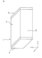
- FIG. 1 is a perspective view showing a first embodiment of an ESD protection apparatus of the present invention.
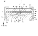
- 2 is an XZ sectional view of FIG. 3 is an XY cross-sectional view of FIG.
- an ESD (Electro-Static Discharge) protection device 1 includes an element body 10, a first discharge electrode 21 provided in the element body 10, and a second discharge.
- the electrode 22 and the discharge auxiliary electrode 50, and the first external electrode 41 and the second external electrode 42 provided on the outer surface of the element body 10 are included.
- the element body 10 is formed in a substantially rectangular parallelepiped shape, and has a length, a width, and a height.
- the length direction of the element body 10 is the X direction
- the width direction of the element body 10 is the Y direction
- the height direction of the element body 10 is the Z direction.
- the outer surface of the element body 10 includes a first end surface 10a, a second end surface 10b located on the opposite side of the first end surface 10a, and a peripheral surface 10c located between the first end surface 10a and the second end surface 10b.
- the first end surface 10a and the second end surface 10b are located in the X direction.
- the element body 10 is configured by laminating a plurality of ceramic layers 11.
- the plurality of ceramic layers 11 are stacked in the Z direction.
- the ceramic layer is made of, for example, a low-temperature co-fired ceramic (LTCC: Low Temperature Co-fired Ceramics) containing Ba, Al, and Si as main components.
- LTCC Low Temperature Co-fired Ceramics
- the ceramic layer may contain at least one of an alkali metal component and a boron component, or may contain a glass component.
- the first discharge electrode 21 and the second discharge electrode 22 face each other in the stacking direction (Z direction) of the plurality of ceramic layers 11.
- the first discharge electrode 21 and the second discharge electrode 22 are arranged at a predetermined distance in the stacking direction.
- the first discharge electrode 21 is connected to the first external electrode 41, and the second discharge electrode 22 is connected to the second external electrode 42.
- the first discharge electrode 21 and the second discharge electrode 22 are each formed in a plate shape extending in the X direction.
- the first discharge electrode 21 and the second discharge electrode 22 are made of an appropriate material such as, for example, Cu, Ag, Pd, Pt, Al, Ni, W, or an alloy containing at least one of them.
- the first end 211 in the longitudinal direction of the first discharge electrode 21 is exposed from the first end face 10 a of the element body 10.
- the second end 212 in the longitudinal direction of the first discharge electrode 21 is located in the element body 10.
- the first end 221 in the longitudinal direction of the second discharge electrode 22 is exposed from the second end face 10 b of the element body 10.
- the second end 222 in the longitudinal direction of the second discharge electrode 22 is located in the element body 10.
- the second end 212 of the first discharge electrode 21 and the second end 222 of the second discharge electrode 22 face each other with a predetermined distance.
- the discharge auxiliary electrode 50 is provided between the first discharge electrode 21 and the second discharge electrode 22 and electrically connects the first discharge electrode 21 and the second discharge electrode 22.
- the discharge auxiliary electrode 50 connects the second end 212 of the first discharge electrode 21 and the second end 222 of the second discharge electrode 22.
- the discharge auxiliary electrode 50 has a first surface direction electrode portion 51 connected to the first discharge electrode 21 and a counter direction electrode portion 60 connected to the first surface direction electrode portion 51.
- the first surface direction electrode portion 51 is provided on the surface of the first discharge electrode 21 facing the second discharge electrode 22 and extends in the surface direction of the first discharge electrode 21.
- the first surface direction electrode portion 51 is formed in a rectangular shape when viewed from the stacking direction.
- the facing direction electrode portion 60 extends in the facing direction (stacking direction) of the first discharge electrode 21 and the second discharge electrode 22.
- the counter-direction electrode unit 60 is disposed in the via hole 12 penetrating in the stacking direction of the element body 10 between the first discharge electrode 21 and the second discharge electrode 22.
- the counter direction electrode part 60 is formed in a truncated cone.
- the height direction of the truncated cone coincides with the stacking direction.
- the bottom surface of the truncated cone contacts the first discharge electrode 21, and the upper surface of the truncated cone contacts the second discharge electrode 22.
- the bottom surface of the truncated cone is smaller than the top surface of the truncated cone.
- the first surface direction electrode portion 51 has a contact surface 51 a that contacts the first discharge electrode 21.
- the contact surface 51a is formed in a rectangular shape.
- the facing direction electrode part 60 has a contact surface 60 a that contacts the first surface direction electrode part 51.
- the contact surface 60a is formed in a circular shape.
- the contact surface 51 a of the first surface direction electrode unit 51 is larger than the contact surface 60 a of the counter direction electrode unit 60. All of the contact surfaces 60a of the counter-direction electrode unit 60 overlap the contact surfaces 51a of the first surface-direction electrode unit 51 when viewed from the stacking direction.
- the discharge auxiliary electrode 50 is composed of, for example, a mixture of a conductive material and an insulating material.
- the conductive material is, for example, a conductor powder.
- the conductive material may be, for example, Cu, Ag, Pd, Pt, Al, Ni, W, or a combination thereof, and may be a material having lower conductivity than a metal material such as a semiconductor material such as SiC powder or a resistance material.
- Insulating materials include, for example, oxides such as Al 2 O 3 , SiO 2 , ZrO 2 , TiO 2 , nitrides such as Si 3 N 4 and AIN, mixed calcined powders of constituent materials of ceramic substrates, glass Substances or combinations thereof may be used.
- the content ratio of the conductive material in the first surface direction electrode portion 51 may be the same as or different from the content ratio of the conductive material in the counter direction electrode portion 60.
- the content ratio of the conductive material of the first surface direction electrode portion 51 may be larger than the content ratio of the conductive material of the counter direction electrode portion 60.
- the first external electrode 41 covers the entire first end surface 10a and the end of the peripheral surface 10c on the first end surface 10a side.
- the first external electrode 41 is in contact with and electrically connected to the first end 211 of the first discharge electrode 21.
- the second external electrode 42 covers all of the second end surface 10b and covers the end portion of the peripheral surface 10c on the second end surface 10b side.
- the second external electrode 42 is in contact with and electrically connected to the first end 221 of the second discharge electrode 22.
- the first external electrode 41 and the second external electrode 42 are made of, for example, an appropriate material such as Cu, Ag, Pd, Pt, Al, Ni, W, or an alloy containing at least one of them.
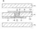
- the first ceramic sheet 111 is provided with a via hole 12 that penetrates the first surface 111a and the second surface 111b.
- the counter-direction electrode unit 60 is filled in the via hole 12.
- the 1st surface direction electrode part 51 is printed on the bottom face of the counter direction electrode part 60, and a part of 1st surface 111a.
- the 1st discharge electrode 21 is printed on the whole surface of the 1st surface direction electrode part 51, and a part of 1st surface 111a.
- the second discharge electrode 22 is printed on a part of the second surface 111b.
- the second ceramic sheet 112 is laminated on the first surface 111 a of the first ceramic sheet 111, and the third ceramic sheet 113 is laminated on the second surface 111 b of the first ceramic sheet 111.
- the first and second external electrodes 21 and 22 are provided on the end faces of the laminated first to third ceramic sheets 111 to 113, and then the whole is fired to manufacture the ESD protection device 1.
- the ESD protection device 1 is used in, for example, an electronic device, and discharges static electricity generated in the electronic device to suppress destruction of the electronic device due to static electricity. More specifically, when the first external electrode 41 is connected to the terminal (primary side) of the electronic device and the second external electrode 42 is connected to the ground (secondary side), the static electricity of the electronic device is the first It is transmitted from the external electrode 41 and the first discharge electrode 21 to the second discharge electrode 22 and the second external electrode 42 via the discharge auxiliary electrode 50.
- the primary side is the side where static electricity is input, and the secondary side is the side where static electricity is output.
- the electrostatic discharge from the first discharge electrode 21 to the second discharge electrode 22 is a discharge due to a current flowing inside the auxiliary discharge electrode 50.
- the ESD protection device 1 when the discharge auxiliary electrode 50 and the first discharge electrode 21 are subjected to thermal shock during ESD application, the coefficient of thermal expansion of the discharge auxiliary electrode 50 and the coefficient of thermal expansion of the first discharge electrode 21 are different. Therefore, thermal stress is generated on the contact surface 51a of the auxiliary discharge electrode 50 with the first discharge electrode 21.
- the contact surface 51a of the first surface direction electrode portion 51 is larger than the contact surface 60a of the counter direction electrode portion 60, the area of the contact surface 51a of the discharge auxiliary electrode 50 is larger than that of the related art.
- connection strength between the auxiliary discharge electrode 50 and the first discharge electrode 21 is improved, and the thermal stress is distributed over the entire contact surface 51a. Then, peeling (delamination) between the discharge auxiliary electrode 50 and the first discharge electrode 21 due to local concentration of thermal stress is prevented, and resistance to ESD application is improved.
- the discharge auxiliary electrode 50 does not have the first surface direction electrode portion 51 but has only the counter direction electrode portion 60 as in the conventional case, the contact surface 60a of the counter direction electrode portion 60 is increased. The material of the discharge auxiliary electrode 50 is wasted. In short, in the present invention, only the portion necessary for improving resistance is enlarged.
- the area of the contact surface 51 a of the discharge auxiliary electrode 50 is increased in a state where the first discharge electrode 21 is connected to the primary side.
- the connection of the electrode 21 is improved, and the ESD response is improved.
- the area of the contact surface 51a of the auxiliary discharge electrode 50 is increased, the electric field concentration on the first surface direction electrode portion 51 is increased and discharge is easily performed.
- the content ratio of the conductive material of the first surface direction electrode portion 51 may be larger than the content ratio of the conductive material of the counter direction electrode portion 60. At this time, the concentration of the electric field on the first surface direction electrode portion 51 is increased, and the discharge becomes easy. Therefore, the discharge start voltage can be lowered and the ESD response can be improved. Furthermore, since the discharge start voltage can be lowered, resistance to ESD application is improved.
- the conductivity of the first surface direction electrode portion 51 can be increased, and the first surface direction electrode portion 51 can be given a discharge property.
- the conductivity of the counter direction electrode portion 60 can be lowered, and the counter direction electrode portion 60 can be provided with insulation. Therefore, the discharge function of the first surface direction electrode part 51 and the insulating function of the counter direction electrode part 60 can be separated.
- FIG. 5 is a sectional view showing a second embodiment of the ESD protection apparatus of the present invention.
- the second embodiment is different from the first embodiment in the configuration of the discharge auxiliary electrode. This different configuration will be described below. Note that in the second embodiment, the same reference numerals as those in the first embodiment have the same configurations as those in the first embodiment, and a description thereof will be omitted.
- the discharge auxiliary electrode 50A of the ESD protection apparatus 1A has a second surface direction electrode portion 52 in addition to the first surface direction electrode portion 51 and the counter direction electrode portion 60 of the first embodiment.
- the second surface direction electrode part 52 is connected between the counter direction electrode part 60 and the second discharge electrode 22.
- the second surface direction electrode portion 52 is provided on the surface of the second discharge electrode 22 facing the first discharge electrode 21 and extends in the surface direction of the second discharge electrode 22.
- the second surface direction electrode portion 52 is formed in a rectangular shape when viewed from the stacking direction.
- the second surface direction electrode portion 52 has a contact surface 52 a that contacts the second discharge electrode 22.
- the contact surface 52a is formed in a rectangular shape.
- the counter direction electrode part 60 has a contact surface 60 b that contacts the second surface direction electrode part 52.
- the contact surface 60b is formed in a circular shape.
- the contact surface 52 a of the second surface direction electrode portion 52 is larger than the contact surface 60 b of the counter direction electrode portion 60. All of the contact surfaces 60 b of the counter direction electrode portion 60 overlap the contact surfaces 52 a of the second surface direction electrode portion 52 when viewed from the stacking direction.
- the first ceramic sheet 111 is provided with a via hole 12 penetrating the first surface 111a and the second surface 111b.
- the counter-direction electrode unit 60 is filled in the via hole 12.
- the 1st surface direction electrode part 51 is printed on the bottom face of the counter direction electrode part 60, and a part of 1st surface 111a.
- the 1st discharge electrode 21 is printed on the whole surface of the 1st surface direction electrode part 51, and a part of 1st surface 111a.
- the second discharge electrode 22 is printed on a part of one surface of the third ceramic sheet 113.
- the second surface direction electrode portion 52 is printed on a part of the second discharge electrode 22.
- the second ceramic sheet 112 is laminated on the first surface 111 a of the first ceramic sheet 111, and the third ceramic sheet 113 is laminated on the second surface 111 b of the first ceramic sheet 111.
- the second surface direction electrode portion 52 is brought into contact with the upper surface of the counter direction electrode portion 60.
- the first and second external electrodes 21 and 22 are provided on the end faces of the laminated first to third ceramic sheets 111 to 113, and then the whole is fired to manufacture the ESD protection device 1A.
- the contact surface 52a of the second surface direction electrode portion 52 is larger than the contact surface 60b of the counter direction electrode portion 60.
- the area of the contact surface 52a with the 50A second discharge electrode 22 is larger than the conventional area. Therefore, the connection strength between the auxiliary discharge electrode 50A and the second discharge electrode 22 is improved. Thereby, peeling between 50 A of discharge auxiliary electrodes and the 2nd discharge electrode 22 is prevented, and the tolerance with respect to ESD application improves.
- FIG. 7 is a cross-sectional view showing a third embodiment of the ESD protection apparatus of the present invention.
- the third embodiment is different from the first embodiment in the configuration of the discharge auxiliary electrode. This different configuration will be described below. Note that in the third embodiment, the same reference numerals as those in the first embodiment have the same configurations as those in the first embodiment, and a description thereof will be omitted.
- the discharge auxiliary electrode 50B of the ESD protection apparatus 1B has a plurality (three in the third embodiment) of counter-direction electrode portions 60.
- the first surface direction electrode portion 51 has a contact surface 51 a that contacts the first discharge electrode 21.
- the facing direction electrode part 60 has a contact surface 60 a that contacts the first surface direction electrode part 51.
- the contact surface 51 a of the first surface direction electrode portion 51 is larger than the contact surfaces 60 a of all the counter direction electrode portions 60.
- the contact surfaces 60a of all the counter-direction electrode portions 60 overlap the contact surfaces 51a of the first surface-direction electrode portions 51 when viewed from the stacking direction.
- the discharge auxiliary electrode 50B has the plurality of counter-direction electrode units 60. Therefore, even if one counter-direction electrode unit 60 stops operating, the other counter-direction electrode unit 60 operates. Therefore, it is possible to prevent the deterioration of responsiveness during ESD application.
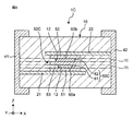
- FIG. 8 is a sectional view showing a fourth embodiment of the ESD protection apparatus of the present invention.
- the fourth embodiment is different from the second embodiment in the configuration of the discharge auxiliary electrode. This different configuration will be described below.
- symbol same as 2nd Embodiment is the same structure as 2nd Embodiment, the description is abbreviate
- the discharge auxiliary electrode 50 ⁇ / b> C of the ESD protection apparatus 1 ⁇ / b> C is a counter-direction electrode different from the configuration of the second embodiment in addition to the first and second surface direction electrode portions 51 and 52 of the second embodiment. Part 60C.
- the counter direction electrode part 60C has a first electrode part 61 on the first discharge electrode 21 side and a second electrode part 62 on the second discharge electrode 22 side. That is, the counter-direction electrode unit 60C is divided into two counter-direction electrode units 60 according to the second embodiment to form first and second electrode units 61 and 62.
- the first and second electrode portions 61 and 62 are disposed in the via holes 12 of the different ceramic layers 11, respectively.
- the third surface direction electrode portion 53 is connected between the first electrode portion 61 and the second electrode portion 62.
- the third surface direction electrode portion 53 extends in a surface direction that intersects the opposing direction of the first discharge electrode 21 and the second discharge electrode 22. That is, the third surface direction electrode portion 53 extends in the XY plane direction intersecting with the Z direction (stacking direction).
- the third surface direction electrode portion 53 is parallel to the first and second surface direction electrode portions 51 and 52 and has the same shape.
- the third surface direction electrode portion 53 is larger than the facing direction electrode portion 60C when viewed from the Z direction.
- the third surface direction electrode portion 53 is connected between the first electrode portion 61 and the second electrode portion 62, so that the third surface direction electrode portion 53 bites into the element body 10. It is possible to prevent peeling between the auxiliary discharge electrode 50C and the element body 10.
- FIG. 9 is a cross-sectional view showing a fifth embodiment of the ESD protection apparatus of the present invention.
- a single ESD protection device is shown, but in the fifth embodiment, a module type ESD protection device is shown.
- the same reference numerals as those in the first embodiment have the same configurations as those in the first embodiment, and a description thereof will be omitted.
- the ESD protection apparatus 1 ⁇ / b> D includes a plurality of sets of the first and second discharge electrodes 21 and 22 and the discharge auxiliary electrode 50 of the first embodiment inside the element body 10.
- a plurality of external electrodes 40 are provided on the outer surface of the element body 10, and the internal electrodes 30 are provided inside the element body 10.
- the internal electrode 30 is connected to the first and second discharge electrodes 21, 22, the discharge auxiliary electrode 50 and the external electrode 40.
- the integrated circuit 5 is mounted on the outer surface of the element body 10, and the integrated circuit 5 is connected to the external electrode 40.
- the module type ESD protection device 1D can improve the resistance to ESD application.
- the present invention is not limited to the above-described embodiment, and the design can be changed without departing from the gist of the present invention.
- the feature points of the first to fifth embodiments may be variously combined.
- the first discharge electrode and the second discharge electrode are provided inside the element body. However, at least one of the first discharge electrode and the second discharge electrode is provided outside the element body. Also good.
- the first discharge electrode is connected to the primary side and the second discharge electrode is connected to the secondary side, but the first discharge electrode is connected to the secondary side and the second discharge The electrode may be connected to the primary side.
- the counter electrode portion is divided into first and second electrode portions, but it may be divided into three or more electrode portions.
- the ceramic material used for the ceramic sheet was a material (BAS material) having a composition centered on Ba, Al, and Si. Each material was prepared and mixed so as to have a predetermined composition, and calcined at 800 ° C. to 1000 ° C. The obtained calcined powder was pulverized with a zirconia ball mill for 12 hours to obtain a ceramic powder. To this ceramic powder, an organic solvent such as toluene and echinene was added and mixed. Furthermore, a binder and a plasticizer were added and mixed to obtain a slurry. The slurry thus obtained was molded by a doctor blade method to obtain a ceramic sheet having a thickness of 10 ⁇ m and a thickness of 50 ⁇ m.
- BAS material a material having a composition centered on Ba, Al, and Si.
- the electrode paste for forming a discharge electrode was produced.
- An electrode paste was obtained by adding a solvent to a binder resin composed of 80 wt% Cu powder having an average particle diameter of about 2 ⁇ m and ethyl cellulose, and stirring and mixing with three rolls.
- a mixed paste for forming the discharge auxiliary electrode was produced.
- a core / shell powder of Cu / Al203 having an average particle diameter of about 2 ⁇ m and a silicon carbide powder having an average particle diameter of 0.5 ⁇ m are mixed at a ratio of 50/50 vol%, a binder resin and a solvent are added, and three rolls are used.
- a mixed paste was obtained by stirring and mixing.
- a binder resin composed of ethyl cellulose or the like and a solvent were 20 wt%, and the remaining 80 wt% was coated Cu powder and silicon carbide powder.
- via hole A via hole having a diameter of 100 ⁇ m was formed on the ceramic sheet by machining or laser processing. There may be a plurality of via holes. By providing a plurality of via holes, even if one counter-direction electrode unit does not operate, the other counter-direction electrode unit operates, so that it is possible to prevent responsiveness deterioration during ESD continuous application. Further, since the thickness of the ceramic sheet becomes a discharge gap, the ESD response is improved as the thickness of the ceramic sheet is reduced. This time, a 10 ⁇ m sheet was used.
- the discharge electrode connected to the external electrode was applied by screen printing.
- the discharge electrode may be directly connected to the external electrode, may be connected via a via hole, or may be connected to a circuit pattern or an integrated circuit.
- the ceramic material used for the ceramic sheet is not particularly limited to the above-described materials, but Al2O3, cordierite, mullite, foresterite, LTCC material obtained by adding glass or the like to CaZrO3, Al2O3, cordierite, HTCC materials such as mullite and forest light, ferrite materials, dielectric materials, and resin materials may be used.
- the material of the discharge electrode may be Ag, Pd, Pt, Al, Ni, W, or a combination thereof other than Cu, but Cu and Ag having high thermal conductivity are desirable.
- the discharge auxiliary electrode may be a single particle or a combination of conductors and semiconductors, or a combination of conductors, semiconductors and insulator particles.
- the conductor particles may have a core-shell structure, a non-core-shell structure, or a combination of both.
- the difference in thermal contraction and thermal expansion coefficient between the discharge electrode and the discharge auxiliary electrode is reduced as compared with the arrangement on one side, and the discharge auxiliary electrode and the discharge electrode are reduced. Delamination is eliminated, the connection is improved, and the ESD response is improved. Further, the difference in thermal expansion coefficient between the discharge electrode and the ceramic layer and the discharge auxiliary electrode when thermal shock is applied during ESD application is reduced, crack generation is suppressed, and ESD continuous application resistance is improved.
- the ceramic layer provided with the counter direction electrode portion has a single layer structure having a thickness of 10 ⁇ m.
- the counter direction electrode portion is divided into two in the stacking direction.
- the ceramic layer provided with the first electrode portion and the ceramic layer provided with the second electrode portion may be separate layers having a thickness of 5 ⁇ m.
- Table 1 shows the characteristic results of the conventional structure and the first and second embodiments.
- the discharge response to ESD was evaluated for 20 samples of the ESD protection device. Responsiveness to ESD was performed by an electrostatic discharge immunity test defined in IEC standard, IEC61000-4-2.
- the voltage applied to the contact discharge was 2, 3, 4, 5, and 6 kV
- the ESD applied voltage that started the discharge was defined as the discharge start voltage. 8kV is performed 100 times, 200 times, 300 times, and 500 times by contact discharge, and when the peak voltage detected on the protection circuit side exceeds 700V, the discharge response is poor (x mark), and the peak voltage is 500V. Discharge responsiveness is acceptable (marked with ⁇ ) for a voltage of ⁇ 700V, good discharge responsiveness is marked for a peak voltage of 300V to 500V (marked with ⁇ ), and discharge responsiveness is particularly good when the peak voltage is less than 300V. ( ⁇ ).
- Numeral 1 indicates a conventional structure, and numerals 2-9 indicate the present invention.
- Table 1 by arranging the surface electrode portion, the amount of the discharge auxiliary electrode around the outer peripheral edge of the via hole where the electric field concentrates when ESD is applied increases, and the electric field is more easily concentrated and the ESD discharge starts. The voltage is lowered.
- the thermal contraction difference and the thermal expansion coefficient difference between the discharge electrode and the discharge auxiliary electrode can be reduced compared to the one side arrangement. Further relax. This eliminates the delamination between the discharge auxiliary electrode and the discharge electrode, improves the connection, and improves the ESD response. Further, the difference in thermal expansion coefficient between the discharge electrode and the ceramic layer and the discharge auxiliary electrode when thermal shock is applied during ESD application is reduced, crack generation is suppressed, and ESD continuous application resistance is improved.
- the counter-direction electrode portion is divided in the stacking direction, that is, when the ceramic layer provided with the counter-direction electrode portion is a plurality of layers, the difference in the thermal expansion coefficient between the discharge electrode and the ceramic layer and the discharge auxiliary electrode is alleviated. Continuous application resistance is improved.
- a mixed paste for forming the counter-direction electrode part filling the via hole was prepared.
- a core / shell powder of Cu / Al203 having an average particle diameter of about 2 ⁇ m and a silicon carbide powder having an average particle diameter of 0.5 ⁇ m are mixed at a ratio of 50/50 vol%, a binder resin and a solvent are added, and three rolls are used.
- a mixed paste was obtained by stirring and mixing.
- a binder resin composed of ethyl cellulose or the like and a solvent were 20 wt%, and the remaining 80 wt% was coated Cu powder and silicon carbide powder.
- a mixed paste for forming the surface direction electrode part was prepared.
- a core / shell powder of Cu / Al203 having an average particle diameter of about 2 ⁇ m and a silicon carbide powder having an average particle diameter of 0.5 ⁇ m are mixed at a ratio of 70/30 vol%, a binder resin and a solvent are added, and three rolls are used.
- a mixed paste was obtained by stirring and mixing.
- a binder resin composed of ethyl cellulose or the like and a solvent were 20 wt%, and the remaining 80 wt% was coated Cu powder and silicon carbide powder.
- Table 2 shows the same measurement conditions as in Table 1.
- Table 2 is different from Table 1 in that the content ratio of the conductive material in the surface direction electrode portion is larger than the content ratio of the conductive material in the counter direction electrode portion.
- ESD protection apparatus 10 Element body 11 Ceramic layer 12 Via hole 21 1st discharge electrode 22 2nd discharge electrode 41 1st external electrode 42 2nd external electrode 50, 50A-50C Discharge auxiliary electrode 51 1st surface direction electrode Part 51a Contact surface 52 Second surface direction electrode part 52a Contact surface 53 Third surface direction electrode part 60, 60C Opposing direction electrode part 60a Contact surface 60b Contact surface 61 First electrode part 62 Second electrode part
Landscapes
- Thermistors And Varistors (AREA)
- Electrostatic Separation (AREA)
Abstract
ESD保護装置は、素体と、互いに対向して配置される第1放電電極および第2放電電極と、第1放電電極と第2放電電極を電気的に接続する放電補助電極とを有する。放電補助電極は、第1放電電極の面方向に延在する第1面方向電極部と、第1放電電極と第2放電電極の対向方向に延在する対向方向電極部とを有する。第1面方向電極部の第1放電電極に接触する接触面は、対向方向電極部の第1面方向電極部に接触する接触面よりも大きい。
Description
本発明は、ESD保護装置に関する。
従来、ESD保護装置としては、WO2010/101103(特許文献1)に記載されたものがある。ESD保護装置は、素体と、素体に設けられ、互いに対向して配置される第1放電電極および第2放電電極と、第1放電電極と第2放電電極の間に設けられ、第1放電電極と第2放電電極を電気的に接続する放電補助電極とを有する。放電補助電極は、第1放電電極と第2放電電極の対向方向に延在する。
ところで、本願発明者は、前記従来のESD保護装置を実際に使用することで、従来のESD保護装置にはESD印加に対する耐性が低いという問題があることを見出した。そして、本願発明者は、この現象を鋭意検討して、以下の原因を突き止めた。
放電補助電極および第1放電電極がESD印加時の熱衝撃を受けると、放電補助電極の熱膨張率と第1放電電極の熱膨張率は異なるため、放電補助電極の第1放電電極との接触面に熱応力が発生する。この熱応力により、放電補助電極と第1放電電極の間で剥がれ(デラミネーション)が発生する。この剥がれにより、ESD印加に対する耐性が低下する。
そこで、本発明の課題は、ESD印加に対する耐性を向上したESD保護装置を提供することにある。
前記課題を解決するため、本発明のESD保護装置は、
素体と、
前記素体に設けられ、互いに対向して配置される第1放電電極および第2放電電極と、
前記第1放電電極と前記第2放電電極の間に設けられ、前記第1放電電極と前記第2放電電極を電気的に接続する放電補助電極と
を備え、
前記放電補助電極は、
前記第1放電電極に接続され、前記第1放電電極の面方向に延在する第1面方向電極部と、
前記第1面方向電極部に接続され、前記第1放電電極と前記第2放電電極の対向方向に延在する対向方向電極部と
を有し、
前記第1面方向電極部の前記第1放電電極に接触する接触面は、前記対向方向電極部の前記第1面方向電極部に接触する接触面よりも大きい。
素体と、
前記素体に設けられ、互いに対向して配置される第1放電電極および第2放電電極と、
前記第1放電電極と前記第2放電電極の間に設けられ、前記第1放電電極と前記第2放電電極を電気的に接続する放電補助電極と
を備え、
前記放電補助電極は、
前記第1放電電極に接続され、前記第1放電電極の面方向に延在する第1面方向電極部と、
前記第1面方向電極部に接続され、前記第1放電電極と前記第2放電電極の対向方向に延在する対向方向電極部と
を有し、
前記第1面方向電極部の前記第1放電電極に接触する接触面は、前記対向方向電極部の前記第1面方向電極部に接触する接触面よりも大きい。
本発明のESD保護装置によれば、放電補助電極は、第1放電電極に接続され、第1放電電極の面方向に延在する第1面方向電極部と、第1面方向電極部に接続され、第1放電電極と第2放電電極の対向方向に延在する対向方向電極部とを有する。第1面方向電極部の第1放電電極に接触する接触面は、対向方向電極部の第1面方向電極部に接触する接触面よりも大きい。
放電補助電極および第1放電電極がESD印加時の熱衝撃を受けると、放電補助電極の熱膨張率と第1放電電極の熱膨張率は異なるため、放電補助電極の第1放電電極との接触面に熱応力が発生する。放電補助電極の接触面の面積は、従来に比べて、大きくなるため、放電補助電極と第1放電電極との接続強度が向上し、熱応力は接触面の全体に分散される。したがって、熱応力が局所的に集中することによる放電補助電極と第1放電電極の間の剥がれ(デラミネーション)を防止して、ESD印加に対する耐性が向上する。
また、ESD保護装置の一実施形態では、
前記放電補助電極は、前記対向方向電極部と前記第2放電電極との間に接続され、前記第2放電電極の面方向に延在する第2面方向電極部を有し、
前記第2面方向電極部の前記第2放電電極に接触する接触面は、前記対向方向電極部の前記第2面方向電極部に接触する接触面よりも大きい。
前記放電補助電極は、前記対向方向電極部と前記第2放電電極との間に接続され、前記第2放電電極の面方向に延在する第2面方向電極部を有し、
前記第2面方向電極部の前記第2放電電極に接触する接触面は、前記対向方向電極部の前記第2面方向電極部に接触する接触面よりも大きい。
前記実施形態によれば、放電補助電極の第2放電電極との接触面の面積は、従来に比べて、大きくなるため、放電補助電極と第2放電電極との接続強度が向上する。したがって、放電補助電極と第2放電電極の間の剥がれを防止して、ESD印加に対する耐性が向上する。
また、ESD保護装置の一実施形態では、前記放電補助電極は、複数の前記対向方向電極部を有する。
前記実施形態によれば、放電補助電極は、複数の対向方向電極部を有するので、1つの対向方向電極部が動作しなくなっても、他の対向方向電極部が動作するため、ESD印加時の応答性の劣化を防止することができる。
また、ESD保護装置の一実施形態では、前記第1面方向電極部の導電材料の含有比率は、前記対向方向電極部の導電材料の含有比率よりも大きい。
前記実施形態によれば、第1面方向電極部の導電材料の含有比率は、対向方向電極部の導電材料の含有比率よりも大きいので、第1放電電極を1次側に接続するとき、第1面方向電極部への電界集中度が増して放電しやすくなる。したがって、放電開始電圧を低くできて、ESD応答性を向上できる。さらに、放電開始電圧を低くできるため、ESD印加に対する耐性が向上する。
また、ESD保護装置の一実施形態では、前記第1放電電極は、1次側に接続され、前記第2放電電極は、2次側に接続される。
ここで、1次側とは、静電気の入力側をいい、2次側とは、静電気の出力側をいう。
前記実施形態によれば、第1放電電極が1次側に接続されている状態で、放電補助電極の第1放電電極との接触面の面積は、大きくなるため、放電補助電極と第1放電電極の接続が良くなり、ESD応答性がよくなる。また、放電補助電極の第1放電電極との接触面の面積は、大きくなるため、第1面方向電極部への電界集中度が増して放電しやすくなる。
また、ESD保護装置の一実施形態では、
前記対向方向電極部は、
前記第1放電電極側の第1電極部と、
前記第2放電電極側の第2電極部と
を有し、
前記第1電極部と前記第2電極部との間に、前記対向方向に交差する面方向に延在する第3面方向電極部が接続される。
前記対向方向電極部は、
前記第1放電電極側の第1電極部と、
前記第2放電電極側の第2電極部と
を有し、
前記第1電極部と前記第2電極部との間に、前記対向方向に交差する面方向に延在する第3面方向電極部が接続される。
前記実施形態によれば、第1電極部と第2電極部との間に、対向方向に交差する面方向に延在する第3面方向電極部が接続されるので、第3面方向電極部を素体に食い込ませることができ、放電補助電極と素体の間の剥がれを防止できる。
本発明のESD保護装置によれば、放電補助電極と第1放電電極の間の剥がれを防止して、ESD印加に対する耐性を向上できる。
以下、本発明を図示の実施の形態により詳細に説明する。
(第1実施形態)
図1は、本発明のESD保護装置の第1実施形態を示す斜視図である。図2は、図1のXZ断面図である。図3は、図1のXY断面図である。図1と図2と図3に示すように、ESD(Electro-Static Discharge:静電気放電)保護装置1は、素体10と、素体10内に設けられた第1放電電極21、第2放電電極22および放電補助電極50と、素体10の外面に設けられた第1外部電極41および第2外部電極42とを有する。
図1は、本発明のESD保護装置の第1実施形態を示す斜視図である。図2は、図1のXZ断面図である。図3は、図1のXY断面図である。図1と図2と図3に示すように、ESD(Electro-Static Discharge:静電気放電)保護装置1は、素体10と、素体10内に設けられた第1放電電極21、第2放電電極22および放電補助電極50と、素体10の外面に設けられた第1外部電極41および第2外部電極42とを有する。
素体10は、略直方体状に形成され、長さと幅と高さを有する。素体10の長さ方向をX方向とし、素体10の幅方向をY方向とし、素体10の高さ方向をZ方向とする。素体10の外面は、第1端面10aと、第1端面10aの反対側に位置する第2端面10bと、第1端面10aと第2端面10bの間に位置する周面10cとを有する。第1端面10aと第2端面10bとは、X方向に位置する。
素体10は、複数のセラミック層11を積層して構成される。複数のセラミック層11は、Z方向に積層される。セラミック層は、例えば、Ba、Al、Siを主成分として含む低温同時焼成セラミック(LTCC:Low Temperature Co-fired Ceramics)から構成される。セラミック層は、アルカリ金属成分およびホウ素成分のうちの少なくとも一方を含んでいてもよく、または、ガラス成分を含んでいてもよい。
第1放電電極21および第2放電電極22は、複数のセラミック層11の積層方向(Z方向)に、互いに対向している。第1放電電極21および第2放電電極22は、積層方向に所定の距離をあけて、配置される。第1放電電極21は、第1外部電極41に接続され、第2放電電極22は、第2外部電極42に接続されている。
第1放電電極21と第2放電電極22は、それぞれ、X方向に延在した板状に形成される。第1放電電極21および第2放電電極22は、例えば、Cu、Ag,Pd,Pt,Al,Ni,Wやそれらの少なくとも一種を含む合金などの適宜の材料により構成される。
第1放電電極21の長手方向の第1端部211は、素体10の第1端面10aから露出している。第1放電電極21の長手方向の第2端部212は、素体10内に位置する。第2放電電極22の長手方向の第1端部221は、素体10の第2端面10bから露出している。第2放電電極22の長手方向の第2端部222は、素体10内に位置する。第1放電電極21の第2端部212と、第2放電電極22の第2端部222とは、所定の距離をあけて、互いに対向している。
放電補助電極50は、第1放電電極21と第2放電電極22の間に設けられ、第1放電電極21と第2放電電極22を電気的に接続する。放電補助電極50は、第1放電電極21の第2端部212と第2放電電極22の第2端部222とを接続する。
放電補助電極50は、第1放電電極21に接続される第1面方向電極部51と、第1面方向電極部51に接続される対向方向電極部60とを有する。
第1面方向電極部51は、第1放電電極21の第2放電電極22に対向する面に設けられ、第1放電電極21の面方向に延在する。第1面方向電極部51は、積層方向からみて、矩形に形成されている。
対向方向電極部60は、第1放電電極21と第2放電電極22の対向方向(積層方向)に延在する。対向方向電極部60は、第1放電電極21と第2放電電極22の間の素体10の積層方向に貫通されたビアホール12に、配置されている。対向方向電極部60は、円錐台に形成されている。円錐台の高さ方向は、積層方向に一致する。円錐台の底面は、第1放電電極21に接触し、円錐台の上面は、第2放電電極22に接触する。円錐台の底面は、円錐台の上面よりも小さい。
第1面方向電極部51は、第1放電電極21に接触する接触面51aを有する。接触面51aは、矩形に形成されている。対向方向電極部60は、第1面方向電極部51に接触する接触面60aを有する。接触面60aは、円形に形成されている。第1面方向電極部51の接触面51aは、対向方向電極部60の接触面60aよりも大きい。対向方向電極部60の接触面60aの全ては、積層方向からみて、第1面方向電極部51の接触面51aに重なる。
放電補助電極50は、例えば、導電材料と絶縁材料との混合物から構成される。導電材料は、例えば、導電体粉である。導電材料は、例えば、Cu、Ag、Pd、Pt、Al、Ni、Wやこれらの組合せでもよく、また、SiC粉等の半導体材料や抵抗材料などの、金属材料よりも導電性の低い材料であってもよい。絶縁材料は、例えば、Al2O3、SiO2、ZrO2、TiO2などの酸化物やSi3N4やAINなどの窒化物や、セラミック基材の構成材料の混合仮焼粉や、ガラス質物質や、これらの組合せでもよい。
第1面方向電極部51の導電材料の含有比率は、対向方向電極部60の導電材料の含有比率と同じであってもよく、または、異なっていてもよい。好ましくは、第1面方向電極部51の導電材料の含有比率は、対向方向電極部60の導電材料の含有比率よりも大きくてもよい。
第1外部電極41は、第1端面10aの全てを覆うと共に周面10cの第1端面10a側の端部を覆う。第1外部電極41は、第1放電電極21の第1端部211に接触して電気的に接続される。第2外部電極42は、第2端面10bの全てを覆うと共に周面10cの第2端面10b側の端部を覆う。第2外部電極42は、第2放電電極22の第1端部221に接触して電気的に接続される。第1外部電極41および第2外部電極42は、例えば、Cu、Ag,Pd,Pt,Al,Ni,Wやそれらの少なくとも一種を含む合金などの適宜の材料により構成される。
次に、前記ESD保護装置1の製造方法について説明する。
図4に示すように、第1セラミックシート111に、その第1面111aおよび第2面111bを貫通するビアホール12を設ける。ビアホール12に、対向方向電極部60を充填する。第1面方向電極部51を、対向方向電極部60の底面と第1面111aの一部に印刷する。第1放電電極21を、第1面方向電極部51の全面と第1面111aの一部に印刷する。第2放電電極22を、第2面111bの一部に印刷する。
その後、第1セラミックシート111の第1面111aに、第2セラミックシート112を積層し、第1セラミックシート111の第2面111bに、第3セラミックシート113を積層する。その後、積層した第1から第3セラミックシート111~113の端面に、第1、第2外部電極21,22を設けてから、全体を焼成して、ESD保護装置1を製造する。
次に、前記ESD保護装置1の動作について説明する。
ESD保護装置1は、例えば、電子機器に用いられ、電子機器に発生する静電気を放電して電子機器の静電気による破壊を抑制する。具体的に述べると、第1外部電極41を電子機器の端子(1次側)に接続し、第2外部電極42をグランド(2次側)に接続したとき、電子機器の静電気は、第1外部電極41および第1放電電極21から、放電補助電極50を介して、第2放電電極22および第2外部電極42に伝わる。1次側は、静電気が入力する側であり、2次側は、静電気が出力する側である。第1放電電極21から第2放電電極22への静電気の放電は、放電補助電極50の内部を流れる電流による放電である。
前記ESD保護装置1によれば、放電補助電極50および第1放電電極21がESD印加時の熱衝撃を受けると、放電補助電極50の熱膨張率と第1放電電極21の熱膨張率は異なるため、放電補助電極50の第1放電電極21との接触面51aに熱応力が発生する。ここで、第1面方向電極部51の接触面51aは、対向方向電極部60の接触面60aよりも大きいので、放電補助電極50の接触面51aの面積は、従来と比べて、大きくなる。
したがって、放電補助電極50と第1放電電極21との接続強度が向上し、熱応力は接触面51aの全体に分散される。そして、熱応力が局所的に集中することによる放電補助電極50と第1放電電極21の間の剥がれ(デラミネーション)を防止して、ESD印加に対する耐性が向上する。
これに対して、従来と同様に、放電補助電極50が、第1面方向電極部51を有さず、対向方向電極部60のみを有する場合、対向方向電極部60の接触面60aを大きくすると、放電補助電極50の材料が無駄となる。要するに、本発明では、耐性の向上に必要な部分のみを大きくしている。
前記ESD保護装置1によれば、第1放電電極21が1次側に接続されている状態で、放電補助電極50の接触面51aの面積は、大きくなるため、放電補助電極50と第1放電電極21の接続が良くなり、ESD応答性がよくなる。また、放電補助電極50の接触面51aの面積は、大きくなるため、第1面方向電極部51への電界集中度が増して放電しやすくなる。
前記ESD保護装置1によれば、第1面方向電極部51の導電材料の含有比率は、対向方向電極部60の導電材料の含有比率よりも大きくてもよい。このとき、第1面方向電極部51への電界集中度が増して放電しやすくなる。したがって、放電開始電圧を低くできて、ESD応答性を向上できる。さらに、放電開始電圧を低くできるため、ESD印加に対する耐性が向上する。
また、第1面方向電極部51の導電性を高くすることができ、第1面方向電極部51に放電性をもたせることができる。一方、対向方向電極部60の導電性を低くすることができ、対向方向電極部60に絶縁性をもたせることができる。したがって、第1面方向電極部51の放電性機能と対向方向電極部60の絶縁性機能とを分けることができる。
(第2実施形態)
図5は、本発明のESD保護装置の第2実施形態を示す断面図である。第2実施形態は、第1実施形態とは、放電補助電極の構成が相違する。この相違する構成を以下に説明する。なお、第2実施形態において、第1実施形態と同一の符号は、第1実施形態と同じ構成であるため、その説明を省略する。
図5は、本発明のESD保護装置の第2実施形態を示す断面図である。第2実施形態は、第1実施形態とは、放電補助電極の構成が相違する。この相違する構成を以下に説明する。なお、第2実施形態において、第1実施形態と同一の符号は、第1実施形態と同じ構成であるため、その説明を省略する。
図5に示すように、ESD保護装置1Aの放電補助電極50Aは、第1実施形態の第1面方向電極部51および対向方向電極部60に加えて、第2面方向電極部52を有する。第2面方向電極部52は、対向方向電極部60と第2放電電極22との間に接続されている。
第2面方向電極部52は、第2放電電極22の第1放電電極21に対向する面に設けられ、第2放電電極22の面方向に延在する。第2面方向電極部52は、積層方向からみて、矩形に形成されている。
第2面方向電極部52は、第2放電電極22に接触する接触面52aを有する。接触面52aは、矩形に形成されている。対向方向電極部60は、第2面方向電極部52に接触する接触面60bを有する。接触面60bは、円形に形成されている。第2面方向電極部52の接触面52aは、対向方向電極部60の接触面60bよりも大きい。対向方向電極部60の接触面60bの全ては、積層方向からみて、第2面方向電極部52の接触面52aに重なる。
次に、前記ESD保護装置1Aの製造方法について説明する。
図6に示すように、第1セラミックシート111に、その第1面111aおよび第2面111bを貫通するビアホール12を設ける。ビアホール12に、対向方向電極部60を充填する。第1面方向電極部51を、対向方向電極部60の底面と第1面111aの一部に印刷する。第1放電電極21を、第1面方向電極部51の全面と第1面111aの一部に印刷する。
第2放電電極22を、第3セラミックシート113の一面の一部に印刷する。第2面方向電極部52を、第2放電電極22の一部に印刷する。
その後、第1セラミックシート111の第1面111aに、第2セラミックシート112を積層し、第1セラミックシート111の第2面111bに、第3セラミックシート113を積層する。このとき、第2面方向電極部52を対向方向電極部60の上面に接触させる。
その後、積層した第1から第3セラミックシート111~113の端面に、第1、第2外部電極21,22を設けてから、全体を焼成して、ESD保護装置1Aを製造する。
前記ESD保護装置1Aによれば、第1実施形態の効果に加え、さらに、第2面方向電極部52の接触面52aは、対向方向電極部60の接触面60bよりも大きいので、放電補助電極50Aの第2放電電極22との接触面52aの面積は、従来と比べて、大きくなる。したがって、放電補助電極50Aと第2放電電極22との接続強度が向上する。これにより、放電補助電極50Aと第2放電電極22の間の剥がれを防止して、ESD印加に対する耐性が向上する。
(第3実施形態)
図7は、本発明のESD保護装置の第3実施形態を示す断面図である。第3実施形態は、第1実施形態とは、放電補助電極の構成が相違する。この相違する構成を以下に説明する。なお、第3実施形態において、第1実施形態と同一の符号は、第1実施形態と同じ構成であるため、その説明を省略する。
図7は、本発明のESD保護装置の第3実施形態を示す断面図である。第3実施形態は、第1実施形態とは、放電補助電極の構成が相違する。この相違する構成を以下に説明する。なお、第3実施形態において、第1実施形態と同一の符号は、第1実施形態と同じ構成であるため、その説明を省略する。
図7に示すように、ESD保護装置1Bの放電補助電極50Bは、複数(第3実施形態では3つ)の対向方向電極部60を有する。第1面方向電極部51は、第1放電電極21に接触する接触面51aを有する。対向方向電極部60は、第1面方向電極部51に接触する接触面60aを有する。
第1面方向電極部51の接触面51aは、全ての対向方向電極部60の接触面60aよりも大きい。全ての対向方向電極部60の接触面60aは、積層方向からみて、第1面方向電極部51の接触面51aに重なる。
前記ESD保護装置1Bによれば、放電補助電極50Bは、複数の対向方向電極部60を有するので、1つの対向方向電極部60が動作しなくなっても、他の対向方向電極部60が動作するため、ESD印加時の応答性の劣化を防止することができる。
(第4実施形態)
図8は、本発明のESD保護装置の第4実施形態を示す断面図である。第4実施形態は、第2実施形態とは、放電補助電極の構成が相違する。この相違する構成を以下に説明する。なお、第4実施形態において、第2実施形態と同一の符号は、第2実施形態と同じ構成であるため、その説明を省略する。
図8は、本発明のESD保護装置の第4実施形態を示す断面図である。第4実施形態は、第2実施形態とは、放電補助電極の構成が相違する。この相違する構成を以下に説明する。なお、第4実施形態において、第2実施形態と同一の符号は、第2実施形態と同じ構成であるため、その説明を省略する。
図8に示すように、ESD保護装置1Cの放電補助電極50Cは、第2実施形態の第1、第2面方向電極部51,52に加えて、第2実施形態の構成と異なる対向方向電極部60Cを有する。
対向方向電極部60Cは、第1放電電極21側の第1電極部61と、第2放電電極22側の第2電極部62とを有する。つまり、対向方向電極部60Cは、第2実施形態の対向方向電極部60を2つに分割して、第1、第2電極部61,62としている。第1、第2電極部61,62は、それぞれ、異なるセラミック層11のビアホール12内に配置される。
第1電極部61と第2電極部62との間に第3面方向電極部53が接続される。第3面方向電極部53は、第1放電電極21と第2放電電極22の対向方向に交差する面方向に延在する。つまり、第3面方向電極部53は、Z方向(積層方向)に交差するXY面方向に延在する。第3面方向電極部53は、第1、第2面方向電極部51,52と平行で、同じ形状である。第3面方向電極部53は、Z方向からみて、対向方向電極部60Cよりも大きい。
前記ESD保護装置1Cによれば、第1電極部61と第2電極部62との間に第3面方向電極部53が接続されるので、第3面方向電極部53を素体10に食い込ませることができ、放電補助電極50Cと素体10の間の剥がれを防止できる。
(第5実施形態)
図9は、本発明のESD保護装置の第5実施形態を示す断面図である。第1実施形態では、単体のESD保護装置を示したが、第5実施形態では、モジュールタイプのESD保護装置を示す。なお、第5実施形態において、第1実施形態と同一の符号は、第1実施形態と同じ構成であるため、その説明を省略する。
図9は、本発明のESD保護装置の第5実施形態を示す断面図である。第1実施形態では、単体のESD保護装置を示したが、第5実施形態では、モジュールタイプのESD保護装置を示す。なお、第5実施形態において、第1実施形態と同一の符号は、第1実施形態と同じ構成であるため、その説明を省略する。
図9に示すように、ESD保護装置1Dは、素体10の内部に、第1実施形態の第1、第2放電電極21,22および放電補助電極50を複数組有する。素体10の外面に、複数の外部電極40が設けられ、素体10の内部に、内部電極30が設けられている。内部電極30は、第1、第2放電電極21,22、放電補助電極50および外部電極40に接続される。素体10の外面には、集積回路5が搭載され、集積回路5は、外部電極40に接続される。
前記ESD保護装置1Cによれば、モジュールタイプのESD保護装置1Dにおいても、ESD印加に対する耐性を向上できる。
なお、本発明は上述の実施形態に限定されず、本発明の要旨を逸脱しない範囲で設計変更可能である。例えば、第1から第5実施形態のそれぞれの特徴点を様々に組み合わせてもよい。
前記実施形態では、第1放電電極および第2放電電極は、素体の内部に設けられているが、第1放電電極および第2放電電極の少なくとも一方が、素体の外部に設けられていてもよい。
前記実施形態では、第1放電電極は、1次側に接続され、第2放電電極は、2次側に接続されているが、第1放電電極は、2次側に接続され、第2放電電極は、1次側に接続されていてもよい。
前記実施形態では、対向方向電極部を第1、第2電極部に分割しているが、3つ以上の電極部に分割してもよい。
[第1実施例]
次に、前記第1実施形態の製造方法の実施例について説明する。
次に、前記第1実施形態の製造方法の実施例について説明する。
(1)セラミックシートの準備
セラミックシートの材料となるセラミック材料には、Ba、Al、Siを中心とした組成からなる材料(BAS材)を用いた。各素材を所定の組成になるよう調合、混合し、800℃~1000℃で仮焼した。得られた仮焼粉末をジルコニアボールミルで12時間粉砕し、セラミック粉末を得た。このセラミック粉末に、トルエン・エキネンなどの有機溶媒を加え混合した。さらに、バインダー、可塑剤を加え混合しスラリーを得た。このようにして得られたスラリーをドクターブレード法により成形し、厚さ10μmと厚さ50μmのセラミックシートを得た。
セラミックシートの材料となるセラミック材料には、Ba、Al、Siを中心とした組成からなる材料(BAS材)を用いた。各素材を所定の組成になるよう調合、混合し、800℃~1000℃で仮焼した。得られた仮焼粉末をジルコニアボールミルで12時間粉砕し、セラミック粉末を得た。このセラミック粉末に、トルエン・エキネンなどの有機溶媒を加え混合した。さらに、バインダー、可塑剤を加え混合しスラリーを得た。このようにして得られたスラリーをドクターブレード法により成形し、厚さ10μmと厚さ50μmのセラミックシートを得た。
(2)放電電極の準備
放電電極を形成するための電極ペーストを作製した。平均粒径約2μmのCu粉80wt%とエチルセルロース等からなるバインダー樹脂に溶剤を添加し、3本ロールで撹拌、混合することで、電極ペーストを得た。
放電電極を形成するための電極ペーストを作製した。平均粒径約2μmのCu粉80wt%とエチルセルロース等からなるバインダー樹脂に溶剤を添加し、3本ロールで撹拌、混合することで、電極ペーストを得た。
(3)放電補助電極の準備
放電補助電極を形成するための混合ペーストを作製した。平均粒径約2μmのCu/Al203のコア/シェル粉と、平均粒径0.5μmの炭化ケイ素粉を、50/50vol%の割合で調合し、バインダー樹脂と溶剤を添加し、3本ロールで撹拌、混合することで、混合ペーストを得た。混合ペーストは、エチルセルロース等からなるバインダー樹脂と溶剤を20wt%とし、残りの80wt%をコートCu粉と炭化ケイ素粉とした。
放電補助電極を形成するための混合ペーストを作製した。平均粒径約2μmのCu/Al203のコア/シェル粉と、平均粒径0.5μmの炭化ケイ素粉を、50/50vol%の割合で調合し、バインダー樹脂と溶剤を添加し、3本ロールで撹拌、混合することで、混合ペーストを得た。混合ペーストは、エチルセルロース等からなるバインダー樹脂と溶剤を20wt%とし、残りの80wt%をコートCu粉と炭化ケイ素粉とした。
(4)ビアホールの形成
セラミックシートに機械加工やレーザー加工でφ100μmのビアホールを形成した。ビアホールは複数個あってもよい。複数個のビアホールを設けることにより、1つの対向方向電極部が動作しなくなっても、他の対向方向電極部が動作するため、ESD連続印加時の応答性の劣化を防止することができる。また、セラミックシートの厚みは、放電ギャップになるため、セラミックシートの厚みが薄いほど、ESD応答性が良くなる。今回は10μmシートを使用した。
セラミックシートに機械加工やレーザー加工でφ100μmのビアホールを形成した。ビアホールは複数個あってもよい。複数個のビアホールを設けることにより、1つの対向方向電極部が動作しなくなっても、他の対向方向電極部が動作するため、ESD連続印加時の応答性の劣化を防止することができる。また、セラミックシートの厚みは、放電ギャップになるため、セラミックシートの厚みが薄いほど、ESD応答性が良くなる。今回は10μmシートを使用した。
(5)積層方向への放電補助電極(対向方向電極部)の形成
ビアホール内へ放電補助電極の対向方向電極部を充填し、その後、乾燥して対向方向電極部を形成した。
ビアホール内へ放電補助電極の対向方向電極部を充填し、その後、乾燥して対向方向電極部を形成した。
(6)面方向への放電補助電極(面方向電極部)の形成
ビアホール上に放電補助電極の面方向電極部をスクリーン印刷によってビアホール径以上の面積で塗布した。今回、ビアホール内の充填と面方向の印刷を別工程で行っているが、スクリーン印刷によって一括で行ってもよい。面方向電極部を、ESDが入力する1次側に配置すると、放電開始側で電界が集中しやすくなり、ESD応答性が良くなる。
ビアホール上に放電補助電極の面方向電極部をスクリーン印刷によってビアホール径以上の面積で塗布した。今回、ビアホール内の充填と面方向の印刷を別工程で行っているが、スクリーン印刷によって一括で行ってもよい。面方向電極部を、ESDが入力する1次側に配置すると、放電開始側で電界が集中しやすくなり、ESD応答性が良くなる。
(7)放電電極の形成
スクリーン印刷によって外部電極に接続される放電電極を塗布した。放電電極は、直接に外部電極と接続されていてもよく、ビアホールを介して接続されていてもよく、回路パターンや集積回路と接続されていてもよい。
スクリーン印刷によって外部電極に接続される放電電極を塗布した。放電電極は、直接に外部電極と接続されていてもよく、ビアホールを介して接続されていてもよく、回路パターンや集積回路と接続されていてもよい。
(8)積層および圧着
セラミックシートを積層し圧着した。ここでは、厚みが0.3mmで中央に放電補助電極が配置されるように、積層した。
セラミックシートを積層し圧着した。ここでは、厚みが0.3mmで中央に放電補助電極が配置されるように、積層した。
(9)カットおよび外部電極形成
LCフィルタのようなチップタイプの電子部品と同様に、マイクロカッタでカットして、各チップにわけた。ここでは、1.0mmx0.5mmになるようにカットした。その後、チップ端面に電極ペーストを塗布し、外部電極を形成した。外部電極の形成は、チップ焼成後に、チップ端面に電極ペーストを塗布、焼き付けしても構わない。
LCフィルタのようなチップタイプの電子部品と同様に、マイクロカッタでカットして、各チップにわけた。ここでは、1.0mmx0.5mmになるようにカットした。その後、チップ端面に電極ペーストを塗布し、外部電極を形成した。外部電極の形成は、チップ焼成後に、チップ端面に電極ペーストを塗布、焼き付けしても構わない。
(10)焼成
次いで、N2雰囲気中で焼成した。酸化しない電極材料(Agなど)の場合には、大気雰囲気でも構わない。
次いで、N2雰囲気中で焼成した。酸化しない電極材料(Agなど)の場合には、大気雰囲気でも構わない。
(11)めっき
LCフィルタのようなチップタイプの電子部品と同様に、外部電極上に電解Ni-Snめっきを行った。
LCフィルタのようなチップタイプの電子部品と同様に、外部電極上に電解Ni-Snめっきを行った。
(12)完成
以上により、ESD保護装置を完成した。なお、セラミックシートに用いるセラミック材料は、特に上記の材料に限定されるものではなく、Al2O3、コーディエライト、ムライト、フォレステライト、CaZrO3にガラスなどを加えたLTCC材料や、Al2O3、コーディエライト、ムライト、フォレストライトなどのHTCC材料、フェライト材料、誘電体材料、樹脂材料でもよい。
以上により、ESD保護装置を完成した。なお、セラミックシートに用いるセラミック材料は、特に上記の材料に限定されるものではなく、Al2O3、コーディエライト、ムライト、フォレステライト、CaZrO3にガラスなどを加えたLTCC材料や、Al2O3、コーディエライト、ムライト、フォレストライトなどのHTCC材料、フェライト材料、誘電体材料、樹脂材料でもよい。
放電電極の材料は、Cu以外に、Ag,Pd,Pt,Al,Ni,Wや、これらの組合せでもよいが、熱伝導率が高いCu,Agが望ましい。
放電補助電極は、導電体、半導体の粒子単体もしくは組み合わせでもよく、導電体、半導体、絶縁体粒子の組み合わせでもよい。導電体の粒子は、コアシェル構造、ノンコアシェル構造でもよく、両方を組み合わせてもよい。厚みがナノメートルの絶縁体のシェルを持つコアシェル構造の粒子を添加することで、ESD応答性を損ねることなく絶縁耐性を保つことが出来る。また、粒子間に結合剤となるガラスもしくは樹脂が介在することで、さらに、絶縁耐性が向上する。
[第2実施例]
次に、前記第2実施形態の製造方法の実施例について説明する。
次に、前記第2実施形態の製造方法の実施例について説明する。
まず、第1実施例の(1)~(5)を行った。
(6)面方向への放電補助電極(面方向電極部)の形成
図6に示すように、ビアホール上にスクリーン印刷した放電補助電極の面方向電極部と、別のセラミックシートにスクリーン印刷した放電補助電極の面方向電極部とを、積み重ねた。ビアホールの上下面に放電補助電極が配置されるため、ESD印加方向に関係なく、ESD応答性が得られる。このため、チップに方向性を付与する必要がなく、製造コストを低減でき、設計に自由度を持たせることができる。
図6に示すように、ビアホール上にスクリーン印刷した放電補助電極の面方向電極部と、別のセラミックシートにスクリーン印刷した放電補助電極の面方向電極部とを、積み重ねた。ビアホールの上下面に放電補助電極が配置されるため、ESD印加方向に関係なく、ESD応答性が得られる。このため、チップに方向性を付与する必要がなく、製造コストを低減でき、設計に自由度を持たせることができる。
また、ビアホールの上下の両側に面方向電極部を配置することにより、片側の配置に比べて、放電電極と放電補助電極の熱収縮差および熱膨張係数差を緩和し、放電補助電極と放電電極のデラミネーションがなくなり、接続が向上して、ESD応答性が良くなる。また、ESD印加時の熱衝撃がかかった際の放電電極およびセラミック層と放電補助電極との熱膨張係数の差を緩和し、クラックの発生を抑制し、ESD連続印加耐性が向上する。
なお、今回、対向方向電極部を設けたセラミック層を、厚さ10μmの1層の構造としたが、第3実施形態のように、対向方向電極部を積層方向に2つに分割した第1、第2電極部として、第1電極部を設けたセラミック層と第2電極部を設けたセラミック層を、厚さ5μmの別の層としてもよい。このように、対向方向電極部を設けるセラミック層を2層とすることで、さらに、放電電極およびセラミック層と放電補助電極の熱膨張係数の差を緩和し、ESD連続印加耐性が向上する。
その後、第1実施例の(9)~(11)を行って、ESD保護装置を完成した。
(実験結果)
次に、従来構造と第1、第2実施例との特性結果を表1に示す。ESD保護装置の20個の試料について、ESDに対する放電応答性を評価した。ESDに対する応答性は、IECの規格、IEC61000-4-2に定められている、静電気放電イミュニティ試験によって行った。
次に、従来構造と第1、第2実施例との特性結果を表1に示す。ESD保護装置の20個の試料について、ESDに対する放電応答性を評価した。ESDに対する応答性は、IECの規格、IEC61000-4-2に定められている、静電気放電イミュニティ試験によって行った。

表1に示すように、接触放電にて2、3、4、5、6kVと印可していき、放電を開始したESD印加電圧を放電開始電圧とした。接触放電にて8kVを100回、200回、300回、500回行って、保護回路側で検出されたピーク電圧が700Vを超えるものを放電応答性が不良(×印)とし、ピーク電圧が500V~700Vのものを放電応答性が可(△印)とし、ピーク電圧が300V~500Vのものを放電応答性が良好(○印)とし、ピーク電圧が300V未満のものを放電応答性が特に良好(◎)と判定した。
番号1は従来構造を示し、番号2~9は本発明を示す。表1からわかるように、面方向電極部を配置することにより、ESD印加時に電界が集中するビアホール外周端の周囲での放電補助電極の量が増加し、より電界が集中しやすくなりESD放電開始電圧が低くなる。
また、対向方向電極部の数量を複数個にすることにより、1つの対向方向電極部が動作しなくなっても、他の対向方向電極部が動作するため、放電開始電圧を維持しながら、ESD連続印加耐性を向上できる。
また、ビアホールの上下の両側(1次側および2次側)に面方向電極部を配置することにより、片側の配置に比べて、放電電極と放電補助電極の熱収縮差および熱膨張係数差をさらに緩和する。これにより、放電補助電極と放電電極のデラミネーションがなくなり、接続が向上して、ESD応答性が良くなる。また、ESD印加時の熱衝撃がかかった際の放電電極およびセラミック層と放電補助電極との熱膨張係数の差を緩和し、クラックの発生を抑制し、ESD連続印加耐性が向上する。
また、対向方向電極部を積層方向に分割する、つまり、対向方向電極部を設けるセラミック層を複数層とすると、放電電極およびセラミック層と放電補助電極との熱膨張係数の差を緩和し、ESD連続印加耐性が向上する。
[第3実施例]
次に、第1、第2実施例において、面方向電極部の導電材料の含有比率を対向方向電極部の導電材料の含有比率よりも大きくするときの、ESD保護装置の製造方法の実施例について説明する。
次に、第1、第2実施例において、面方向電極部の導電材料の含有比率を対向方向電極部の導電材料の含有比率よりも大きくするときの、ESD保護装置の製造方法の実施例について説明する。
まず、第1実施例の(1)(2)を行った。
(3)放電補助電極の準備
ビアホールに充填する対向方向電極部を形成するための混合ペーストを作製した。平均粒径約2μmのCu/Al203のコア/シェル粉と、平均粒径0.5μmの炭化ケイ素粉を、50/50vol%の割合で調合し、バインダー樹脂と溶剤を添加し、3本ロールで撹拌、混合することで、混合ペーストを得た。混合ペーストは、エチルセルロース等からなるバインダー樹脂と溶剤を20wt%とし、残りの80wt%をコートCu粉と炭化ケイ素粉とした。
ビアホールに充填する対向方向電極部を形成するための混合ペーストを作製した。平均粒径約2μmのCu/Al203のコア/シェル粉と、平均粒径0.5μmの炭化ケイ素粉を、50/50vol%の割合で調合し、バインダー樹脂と溶剤を添加し、3本ロールで撹拌、混合することで、混合ペーストを得た。混合ペーストは、エチルセルロース等からなるバインダー樹脂と溶剤を20wt%とし、残りの80wt%をコートCu粉と炭化ケイ素粉とした。
面方向電極部を形成するための混合ペーストを作製した。平均粒径約2μmのCu/Al203のコア/シェル粉と、平均粒径0.5μmの炭化ケイ素粉を、70/30vol%の割合で調合し、バインダー樹脂と溶剤を添加し、3本ロールで撹拌、混合することで、混合ペーストを得た。混合ペーストは、エチルセルロース等からなるバインダー樹脂と溶剤を20wt%とし、残りの80wt%をコートCu粉と炭化ケイ素粉とした。
その後、第1実施例の(4)~(11)を行って、ESD保護装置を完成した。
(実験結果)
次に、第3実施例の特性結果を表2に示す。表2は、表1と同じ測定条件である。表2は、表1とは、面方向電極部の導電材料の含有比率が対向方向電極部の導電材料の含有比率よりも大きい点が異なる。
次に、第3実施例の特性結果を表2に示す。表2は、表1と同じ測定条件である。表2は、表1とは、面方向電極部の導電材料の含有比率が対向方向電極部の導電材料の含有比率よりも大きい点が異なる。
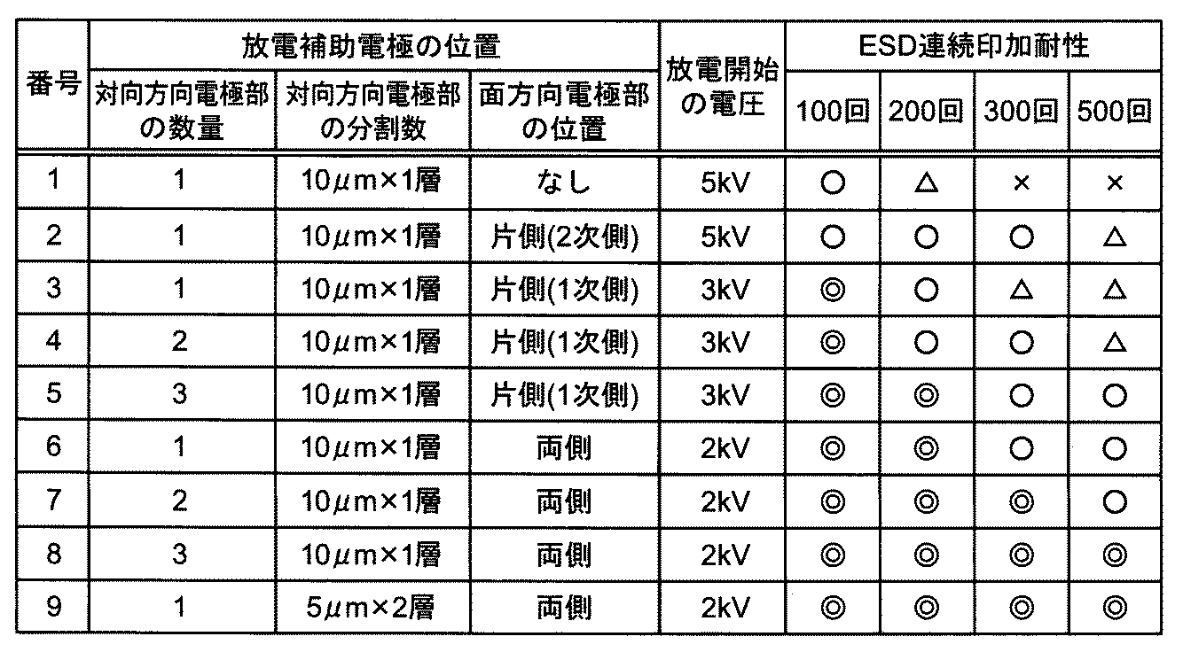
表2からわかるように、面方向電極部の導電材料の含有比率を対向方向電極部の導電材料の含有比率よりも大きくすることで、放電補助電極への電界集中度が増して、放電しやすくなる。つまり、表2では、表1(第1、第2実施例)に比較して、放電開始電圧が低くなっている。このように、放電開始電圧が低くなっているため、ESD連続印加耐性も向上している。
1,1A~1D ESD保護装置
10 素体
11 セラミック層
12 ビアホール
21 第1放電電極
22 第2放電電極
41 第1外部電極
42 第2外部電極
50,50A~50C 放電補助電極
51 第1面方向電極部
51a 接触面
52 第2面方向電極部
52a 接触面
53 第3面方向電極部
60,60C 対向方向電極部
60a 接触面
60b 接触面
61 第1電極部
62 第2電極部
10 素体
11 セラミック層
12 ビアホール
21 第1放電電極
22 第2放電電極
41 第1外部電極
42 第2外部電極
50,50A~50C 放電補助電極
51 第1面方向電極部
51a 接触面
52 第2面方向電極部
52a 接触面
53 第3面方向電極部
60,60C 対向方向電極部
60a 接触面
60b 接触面
61 第1電極部
62 第2電極部
Claims (6)
- 素体と、
前記素体に設けられ、互いに対向して配置される第1放電電極および第2放電電極と、
前記第1放電電極と前記第2放電電極の間に設けられ、前記第1放電電極と前記第2放電電極を電気的に接続する放電補助電極と
を備え、
前記放電補助電極は、
前記第1放電電極に接続され、前記第1放電電極の面方向に延在する第1面方向電極部と、
前記第1面方向電極部に接続され、前記第1放電電極と前記第2放電電極の対向方向に延在する対向方向電極部と
を有し、
前記第1面方向電極部の前記第1放電電極に接触する接触面は、前記対向方向電極部の前記第1面方向電極部に接触する接触面よりも大きい、ESD保護装置。 - 前記放電補助電極は、前記対向方向電極部と前記第2放電電極との間に接続され、前記第2放電電極の面方向に延在する第2面方向電極部を有し、
前記第2面方向電極部の前記第2放電電極に接触する接触面は、前記対向方向電極部の前記第2面方向電極部に接触する接触面よりも大きい、請求項1に記載のESD保護装置。 - 前記放電補助電極は、複数の前記対向方向電極部を有する、請求項1または2に記載のESD保護装置。
- 前記第1面方向電極部の導電材料の含有比率は、前記対向方向電極部の導電材料の含有比率よりも大きい、請求項1から3の何れか一つに記載のESD保護装置。
- 前記第1放電電極は、1次側に接続され、前記第2放電電極は、2次側に接続される、請求項1から4の何れか一つに記載のESD保護装置。
- 前記対向方向電極部は、
前記第1放電電極側の第1電極部と、
前記第2放電電極側の第2電極部と
を有し、
前記第1電極部と前記第2電極部との間に、前記対向方向に交差する面方向に延在する第3面方向電極部が接続される、請求項1から5の何れか一つに記載のESD保護装置。
Priority Applications (2)
| Application Number | Priority Date | Filing Date | Title |
|---|---|---|---|
| CN201690000577.5U CN207368416U (zh) | 2015-06-15 | 2016-06-02 | Esd保护装置 |
| JP2017524808A JP6428938B2 (ja) | 2015-06-15 | 2016-06-02 | Esd保護装置 |
Applications Claiming Priority (2)
| Application Number | Priority Date | Filing Date | Title |
|---|---|---|---|
| JP2015-120058 | 2015-06-15 | ||
| JP2015120058 | 2015-06-15 |
Publications (1)
| Publication Number | Publication Date |
|---|---|
| WO2016203976A1 true WO2016203976A1 (ja) | 2016-12-22 |
Family
ID=57545250
Family Applications (1)
| Application Number | Title | Priority Date | Filing Date |
|---|---|---|---|
| PCT/JP2016/066430 Ceased WO2016203976A1 (ja) | 2015-06-15 | 2016-06-02 | Esd保護装置 |
Country Status (3)
| Country | Link |
|---|---|
| JP (1) | JP6428938B2 (ja) |
| CN (1) | CN207368416U (ja) |
| WO (1) | WO2016203976A1 (ja) |
Cited By (1)
| Publication number | Priority date | Publication date | Assignee | Title |
|---|---|---|---|---|
| JP2018148121A (ja) * | 2017-03-08 | 2018-09-20 | アルプス電気株式会社 | 高周波モジュール |
Citations (3)
| Publication number | Priority date | Publication date | Assignee | Title |
|---|---|---|---|---|
| JP2010231909A (ja) * | 2009-03-26 | 2010-10-14 | Panasonic Corp | 過電圧保護部品およびその製造方法 |
| WO2011096335A1 (ja) * | 2010-02-04 | 2011-08-11 | 株式会社 村田製作所 | Esd保護装置の製造方法及びesd保護装置 |
| WO2013054629A1 (ja) * | 2011-10-14 | 2013-04-18 | Tdk株式会社 | 静電気対策素子 |
Family Cites Families (2)
| Publication number | Priority date | Publication date | Assignee | Title |
|---|---|---|---|---|
| US20110317326A1 (en) * | 2009-03-05 | 2011-12-29 | Showa Denlo K.K. | Discharge gap filling composition and electrostatic discharge protector |
| CN107257087B (zh) * | 2013-06-24 | 2020-01-03 | 株式会社村田制作所 | Esd保护装置 |
-
2016
- 2016-06-02 WO PCT/JP2016/066430 patent/WO2016203976A1/ja not_active Ceased
- 2016-06-02 JP JP2017524808A patent/JP6428938B2/ja active Active
- 2016-06-02 CN CN201690000577.5U patent/CN207368416U/zh active Active
Patent Citations (3)
| Publication number | Priority date | Publication date | Assignee | Title |
|---|---|---|---|---|
| JP2010231909A (ja) * | 2009-03-26 | 2010-10-14 | Panasonic Corp | 過電圧保護部品およびその製造方法 |
| WO2011096335A1 (ja) * | 2010-02-04 | 2011-08-11 | 株式会社 村田製作所 | Esd保護装置の製造方法及びesd保護装置 |
| WO2013054629A1 (ja) * | 2011-10-14 | 2013-04-18 | Tdk株式会社 | 静電気対策素子 |
Cited By (1)
| Publication number | Priority date | Publication date | Assignee | Title |
|---|---|---|---|---|
| JP2018148121A (ja) * | 2017-03-08 | 2018-09-20 | アルプス電気株式会社 | 高周波モジュール |
Also Published As
| Publication number | Publication date |
|---|---|
| CN207368416U (zh) | 2018-05-15 |
| JPWO2016203976A1 (ja) | 2017-12-21 |
| JP6428938B2 (ja) | 2018-11-28 |
Similar Documents
| Publication | Publication Date | Title |
|---|---|---|
| KR101392455B1 (ko) | Esd 보호 디바이스 및 그 제조 방법 | |
| KR101254212B1 (ko) | Esd 보호 디바이스 | |
| JP5459295B2 (ja) | Esd保護デバイスおよびその製造方法 | |
| WO2014208215A1 (ja) | Esd保護装置 | |
| JP5561370B2 (ja) | Esd保護デバイスおよびその製造方法 | |
| CN207834827U (zh) | Esd保护器件 | |
| JP6428938B2 (ja) | Esd保護装置 | |
| CN204947322U (zh) | Esd保护器件 | |
| JP6390816B2 (ja) | Esd保護装置 | |
| US10292249B2 (en) | ESD protection device | |
| JP5605413B2 (ja) | Esd保護デバイスとその製造方法 | |
| CN105340141B (zh) | Esd保护装置 | |
| JP2017010850A (ja) | Esd保護装置 | |
| JP6048055B2 (ja) | Esd保護デバイスとその製造方法 | |
| JP6406450B2 (ja) | Esd保護装置およびesd保護装置の製造方法 | |
| CN208093946U (zh) | Esd保护装置 | |
| JP5614563B2 (ja) | Esd保護デバイスの製造方法 |
Legal Events
| Date | Code | Title | Description |
|---|---|---|---|
| 121 | Ep: the epo has been informed by wipo that ep was designated in this application |
Ref document number: 16811451 Country of ref document: EP Kind code of ref document: A1 |
|
| ENP | Entry into the national phase |
Ref document number: 2017524808 Country of ref document: JP Kind code of ref document: A |
|
| NENP | Non-entry into the national phase |
Ref country code: DE |
|
| 122 | Ep: pct application non-entry in european phase |
Ref document number: 16811451 Country of ref document: EP Kind code of ref document: A1 |