WO2016203812A1 - 光学装置、及び光学装置の製造方法 - Google Patents
光学装置、及び光学装置の製造方法 Download PDFInfo
- Publication number
- WO2016203812A1 WO2016203812A1 PCT/JP2016/061013 JP2016061013W WO2016203812A1 WO 2016203812 A1 WO2016203812 A1 WO 2016203812A1 JP 2016061013 W JP2016061013 W JP 2016061013W WO 2016203812 A1 WO2016203812 A1 WO 2016203812A1
- Authority
- WO
- WIPO (PCT)
- Prior art keywords
- lid
- optical
- side wall
- lid portion
- optical device
- Prior art date
- Legal status (The legal status is an assumption and is not a legal conclusion. Google has not performed a legal analysis and makes no representation as to the accuracy of the status listed.)
- Ceased
Links
Images



Classifications
-
- H—ELECTRICITY
- H10—SEMICONDUCTOR DEVICES; ELECTRIC SOLID-STATE DEVICES NOT OTHERWISE PROVIDED FOR
- H10F—INORGANIC SEMICONDUCTOR DEVICES SENSITIVE TO INFRARED RADIATION, LIGHT, ELECTROMAGNETIC RADIATION OF SHORTER WAVELENGTH OR CORPUSCULAR RADIATION
- H10F39/00—Integrated devices, or assemblies of multiple devices, comprising at least one element covered by group H10F30/00, e.g. radiation detectors comprising photodiode arrays
- H10F39/80—Constructional details of image sensors
- H10F39/806—Optical elements or arrangements associated with the image sensors
-
- H—ELECTRICITY
- H10—SEMICONDUCTOR DEVICES; ELECTRIC SOLID-STATE DEVICES NOT OTHERWISE PROVIDED FOR
- H10F—INORGANIC SEMICONDUCTOR DEVICES SENSITIVE TO INFRARED RADIATION, LIGHT, ELECTROMAGNETIC RADIATION OF SHORTER WAVELENGTH OR CORPUSCULAR RADIATION
- H10F39/00—Integrated devices, or assemblies of multiple devices, comprising at least one element covered by group H10F30/00, e.g. radiation detectors comprising photodiode arrays
- H10F39/011—Manufacture or treatment of image sensors covered by group H10F39/12
- H10F39/024—Manufacture or treatment of image sensors covered by group H10F39/12 of coatings or optical elements
-
- H—ELECTRICITY
- H10—SEMICONDUCTOR DEVICES; ELECTRIC SOLID-STATE DEVICES NOT OTHERWISE PROVIDED FOR
- H10F—INORGANIC SEMICONDUCTOR DEVICES SENSITIVE TO INFRARED RADIATION, LIGHT, ELECTROMAGNETIC RADIATION OF SHORTER WAVELENGTH OR CORPUSCULAR RADIATION
- H10F39/00—Integrated devices, or assemblies of multiple devices, comprising at least one element covered by group H10F30/00, e.g. radiation detectors comprising photodiode arrays
- H10F39/80—Constructional details of image sensors
- H10F39/804—Containers or encapsulations
-
- H—ELECTRICITY
- H10—SEMICONDUCTOR DEVICES; ELECTRIC SOLID-STATE DEVICES NOT OTHERWISE PROVIDED FOR
- H10F—INORGANIC SEMICONDUCTOR DEVICES SENSITIVE TO INFRARED RADIATION, LIGHT, ELECTROMAGNETIC RADIATION OF SHORTER WAVELENGTH OR CORPUSCULAR RADIATION
- H10F77/00—Constructional details of devices covered by this subclass
-
- G—PHYSICS
- G02—OPTICS
- G02F—OPTICAL DEVICES OR ARRANGEMENTS FOR THE CONTROL OF LIGHT BY MODIFICATION OF THE OPTICAL PROPERTIES OF THE MEDIA OF THE ELEMENTS INVOLVED THEREIN; NON-LINEAR OPTICS; FREQUENCY-CHANGING OF LIGHT; OPTICAL LOGIC ELEMENTS; OPTICAL ANALOGUE/DIGITAL CONVERTERS
- G02F1/00—Devices or arrangements for the control of the intensity, colour, phase, polarisation or direction of light arriving from an independent light source, e.g. switching, gating or modulating; Non-linear optics
- G02F1/01—Devices or arrangements for the control of the intensity, colour, phase, polarisation or direction of light arriving from an independent light source, e.g. switching, gating or modulating; Non-linear optics for the control of the intensity, phase, polarisation or colour
- G02F1/13—Devices or arrangements for the control of the intensity, colour, phase, polarisation or direction of light arriving from an independent light source, e.g. switching, gating or modulating; Non-linear optics for the control of the intensity, phase, polarisation or colour based on liquid crystals, e.g. single liquid crystal display cells
- G02F1/133—Constructional arrangements; Operation of liquid crystal cells; Circuit arrangements
- G02F1/1333—Constructional arrangements; Manufacturing methods
- G02F1/133308—Support structures for LCD panels, e.g. frames or bezels
- G02F1/133311—Environmental protection, e.g. against dust or humidity
-
- G—PHYSICS
- G02—OPTICS
- G02F—OPTICAL DEVICES OR ARRANGEMENTS FOR THE CONTROL OF LIGHT BY MODIFICATION OF THE OPTICAL PROPERTIES OF THE MEDIA OF THE ELEMENTS INVOLVED THEREIN; NON-LINEAR OPTICS; FREQUENCY-CHANGING OF LIGHT; OPTICAL LOGIC ELEMENTS; OPTICAL ANALOGUE/DIGITAL CONVERTERS
- G02F1/00—Devices or arrangements for the control of the intensity, colour, phase, polarisation or direction of light arriving from an independent light source, e.g. switching, gating or modulating; Non-linear optics
- G02F1/01—Devices or arrangements for the control of the intensity, colour, phase, polarisation or direction of light arriving from an independent light source, e.g. switching, gating or modulating; Non-linear optics for the control of the intensity, phase, polarisation or colour
- G02F1/13—Devices or arrangements for the control of the intensity, colour, phase, polarisation or direction of light arriving from an independent light source, e.g. switching, gating or modulating; Non-linear optics for the control of the intensity, phase, polarisation or colour based on liquid crystals, e.g. single liquid crystal display cells
- G02F1/133—Constructional arrangements; Operation of liquid crystal cells; Circuit arrangements
- G02F1/136—Liquid crystal cells structurally associated with a semi-conducting layer or substrate, e.g. cells forming part of an integrated circuit
- G02F1/1362—Active matrix addressed cells
- G02F1/136277—Active matrix addressed cells formed on a semiconductor substrate, e.g. of silicon
-
- G—PHYSICS
- G02—OPTICS
- G02F—OPTICAL DEVICES OR ARRANGEMENTS FOR THE CONTROL OF LIGHT BY MODIFICATION OF THE OPTICAL PROPERTIES OF THE MEDIA OF THE ELEMENTS INVOLVED THEREIN; NON-LINEAR OPTICS; FREQUENCY-CHANGING OF LIGHT; OPTICAL LOGIC ELEMENTS; OPTICAL ANALOGUE/DIGITAL CONVERTERS
- G02F1/00—Devices or arrangements for the control of the intensity, colour, phase, polarisation or direction of light arriving from an independent light source, e.g. switching, gating or modulating; Non-linear optics
- G02F1/29—Devices or arrangements for the control of the intensity, colour, phase, polarisation or direction of light arriving from an independent light source, e.g. switching, gating or modulating; Non-linear optics for the control of the position or the direction of light beams, i.e. deflection
-
- G—PHYSICS
- G02—OPTICS
- G02F—OPTICAL DEVICES OR ARRANGEMENTS FOR THE CONTROL OF LIGHT BY MODIFICATION OF THE OPTICAL PROPERTIES OF THE MEDIA OF THE ELEMENTS INVOLVED THEREIN; NON-LINEAR OPTICS; FREQUENCY-CHANGING OF LIGHT; OPTICAL LOGIC ELEMENTS; OPTICAL ANALOGUE/DIGITAL CONVERTERS
- G02F2203/00—Function characteristic
- G02F2203/12—Function characteristic spatial light modulator
Definitions
- the present invention relates to an optical device in which an optical element is sealed, and a manufacturing method thereof.
- an optical device in which an optical element is arranged in a housing and a lid is attached and hermetically sealed in order to suppress the influence of humidity or the like on the optical element is known.
- Some of such optical devices have a structure in which an opening is provided in the lid portion, and the opening is closed with an optical window that is a light-transmitting material to form an optical path (see, for example, Patent Document 1).
- FIG. 4A and 4B are diagrams showing a schematic configuration of a conventional optical device 100 in which the optical element 11 is sealed, in which FIG. 4A is a cross-sectional view with a lid portion opened, and FIG. 4B is a perspective view.
- the optical device 100 includes an optical element 11 including a light receiving portion 1a and a semiconductor element 11b, a substrate 20, a side wall portion 40, and a lid portion 50.
- An electrode terminal 30 is formed on the substrate 20, and the electrode terminal 30 is wire-bonded to the semiconductor element 11 b with a wire 70.
- the lid portion 50 has a frame portion 60 made of a light non-transmissive material in which an opening 61 is formed, and an optical window 62 made of a light transmissive material that closes the opening 61.
- the light receiving unit 11a functions as an effective region having an optical function.
- light is incident on the light receiving portion 11a.
- the light receiving portion 11a can be both a light incident member and a light emitting member. It may be a member.
- the optical window 62 serves as an optical path for incident light to the light receiving unit 11a or outgoing light from the light receiving unit 11a.
- the lid portion 50 is attached to the side wall portion 40 and hermetically sealed.
- JP 9-148469 A Japanese Patent Publication “JP 9-148469 A” (published June 6, 1997)
- the inside of the optical device 100 cannot be processed after hermetically sealing. Therefore, internal processing is performed before the lid 50 is attached to the side wall 40, but since the optical element 11 is exposed, each step is performed in a state where foreign matter is likely to adhere to and accumulate on the optical element 11. . Examples of such foreign substances include those entering from the outside and wire scraps in the wire bonding process. In the wire bonding process, since the bonding apparatus is operated with the optical element 11 exposed, the possibility of foreign matter adhering to the optical element 11 becomes very high.
- the optical element 11 when a foreign object adheres to the light receiving part 11a of the optical element 11, the amount or direction of the incident light to the light receiving part 11a or the outgoing light from the light receiving part 11a changes due to the foreign object. Element 11 will not function correctly. For example, in the case where the optical element 11 is a spatial light modulation element having a function of controlling the angle of reflected light, crosstalk occurs due to the incident light being refracted by a foreign substance, causing malfunction (output abnormality). . Further, when the optical element 11 is a solid-state image sensor, the amount of received light is significantly reduced due to light being refracted by a foreign substance.
- the present invention has been made in view of the above problems, and an object of the present invention is to protect an effective area of an optical element from foreign matter, and to suppress an optical element performance degradation due to the foreign matter, and a method for manufacturing the same. Is to provide.
- an optical device includes an optical element, a substrate on which the optical element is mounted and on which an electrode terminal is formed, a side wall portion surrounding the optical element and the electrode terminal, An optical device including a lid portion fixed to a side wall portion and facing the substrate, wherein the lid portion is provided with an optical window, and the side wall portion is provided so that the optical window covers an effective area of the optical element.
- an optical device capable of protecting the effective area of the optical element from foreign matter and suppressing the performance degradation of the optical element due to the foreign matter.
- FIG. 1 is sectional drawing which shows schematic structure of the optical apparatus of Embodiment 1 of this invention, (b) is the top view, (c) is the perspective view. It is sectional drawing which shows schematic structure of the optical apparatus of Embodiment 2 of this invention. It is sectional drawing which shows schematic structure of the optical apparatus of Embodiment 3 of this invention. (A) is sectional drawing which shows schematic structure of the conventional optical apparatus, (b) is the perspective view.
- FIG. 1A and 1B are diagrams illustrating a schematic configuration of an optical device 10 according to the present embodiment.
- FIG. 1A is a cross-sectional view
- FIG. 1B is a top view
- FIG. 1C is a perspective view.
- FIG. 1A shows the optical device 10 in a state where a second lid 6 described below is removed (a state before being fixed).
- the optical device 10 includes an LCOS element 1, a substrate 2, a side wall portion 4, and a lid portion 8.
- the LCOS element 1 is a spatial light modulation element having a function of controlling the angle of reflected light, and includes a semiconductor element 1b and a light receiving portion 1a.
- the semiconductor element 1b has a drive circuit for driving the light receiving portion 1a formed on a silicon substrate, and the boundary surface with the light receiving portion 1a is formed in a mirror shape.
- the light receiving unit 1a includes a liquid crystal layer and a glass layer, and is stacked on the semiconductor element 1b in the order of description.
- the LCOS element 1 changes the orientation of the liquid crystal according to the change in the voltage applied to the liquid crystal layer, and changes the reflection angle of the light incident on the light receiving unit 1a. That is, the reflection angle can be controlled by controlling the voltage.
- the light-receiving unit 1a functions as an effective region having an optical function.
- the substrate 2 is a member for mounting the LCOS element 1.
- it is made of ceramic, metal or the like.
- an electrode terminal 3 is formed on the substrate 2 for electrical connection with the outside.
- the electrode terminal 3 and the semiconductor element 1 b of the LCOS element 1 are connected by wire bonding using a wire 7.
- a wire 7 For example, gold, aluminum, or the like is used for the wire 7.
- the side wall part 4 is a frame-like member provided on the substrate 2 so as to surround the LCOS element 1 and is made of, for example, ceramic, metal or the like. In addition, you may form in frame shape from several members.
- the side wall 4 may be formed integrally with the substrate 2 or may be formed as a separate body. When formed as a separate body, for example, the side wall 4 is fixed to the substrate 2 with resin.
- a heater substrate may be provided between the substrate 2 and the LCOS element 1.
- the alignment speed of the liquid crystal can be increased from room temperature.
- conduction to the heater substrate can also be performed via the electrode terminal 3 by wire bonding.
- the lid portion 8 is a member that is fixed to the side wall portion 4 and covers the substrate 2. That is, the optical device 10 is a device in which the LCOS element 1 is sealed in a housing (package) including the substrate 2, the side wall portion 4, and the lid portion 8.
- the lid portion 8 is divided into a first lid portion 5 and a second lid portion 6.
- the first lid part 5 has a frame part 51 in which an opening 53 is formed and an optical window 52.
- the frame part 51 is formed from a non-light-transmissive metal material.
- the opening 53 is closed by an optical window 52 formed from a light transmissive material (for example, a glass substrate).
- the optical window 52 is arrange
- the second lid portion 6 is formed of a non-light-transmissive metal material, is disposed at a position covering the electrode terminal 3 and the wire 7, and is fixed to the side wall portion 4.
- the lid portion 8 since the lid portion 8 is divided into the first lid portion 5 and the second lid portion 6, the lid portion 8 can be attached to the side wall portion 4 in two steps. Therefore, from the time when the first lid portion 5 is attached to the side wall portion 4 until the second lid portion 6 is attached, the light receiving portion 1a of the LCOS element 1 is covered by the first lid portion 5 to protect the light receiving portion 1a. In this state, the electrode terminal 3 and the semiconductor element 1b can be wire-bonded. Furthermore, LCOS element 1 can be sealed by attaching the 2nd cover part 6 to the side wall part 4 after that.
- the light receiving portion 1a of the LCOS element 1 can be protected from foreign matters, and the performance degradation of the optical elements due to the foreign matters can be suppressed.
- the 2nd cover part 6 is provided with the convex part 61 which covers a part of 1st cover part 5, and the 2nd cover part 6 is this convex part.
- the first lid 5 is overlapped and fixed.
- the first lid portion 5 and the second lid portion 6 at least partially overlap each other, whereby the first lid portion 5 and the second lid portion 6 can be firmly fixed to each other.
- the element 1 can be reliably sealed.
- the first lid portion 5 and the second lid portion 6 are at least partially overlapped, when fixing each other by welding, welding is performed rather than attaching only the end faces together. easy.
- the LCOS element 1 is mounted on the substrate 2 to which the side wall portion 4 is attached (or on the substrate 2 having the side wall portion 4).
- the first lid portion 5 is fixed to the side wall portion 4 so that the optical window 52 of the first lid portion 5 covers the light receiving portion 1a of the LCOS element 1 (first lid portion attaching step).
- the semiconductor element 1b and the electrode terminal 3 are wire-bonded with the wire 7 (connection process). At this time, wire bonding can be performed in a state where the light receiving unit 1a is protected from foreign substances by the first lid unit 5.
- the second lid portion 6 is fixed to the side wall portion 4 and the first lid portion 5 so as to cover the electrode terminal 3 and the wire 7 (second lid portion attaching step).
- the optical device 10 having the LCOS element 1 sealed therein can be manufactured.
- the first lid 5 and the second lid 6 are fixed by seam welding.
- the above fixing may be performed by resin bonding.
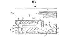
- FIG. 2 is a schematic cross-sectional view of the optical device 10A of the present embodiment.
- optical device 10A shown in FIG. Since the other configuration of the optical device 10A is the same as the configuration of the optical device 10, the same components are denoted by the same reference numerals, and the description thereof is omitted.
- the lid portion 8A has a first lid portion 5A and a second lid portion 6.
- the second lid 6 is the same as the second lid 6 included in the lid 8 of the optical device 10.
- FIG. 2 shows the optical device 10 ⁇ / b> A with the second lid 6 removed.
- a top view and a perspective view of the optical device 10A in a state where the second lid portion 6 is closed are the same as (b) and (c) of FIG. 1, respectively.
- the first lid 5 ⁇ / b> A includes a partition 51 a in addition to the configuration of the first lid 5.
- the partition 51 a has a shape protruding from the frame 51 toward the substrate 2, and is a partition provided to separate the light receiving unit 1 a from the electrode terminal 3 and the wire 7.
- the partition 51a is made of a material different from that of the frame 51 and is fixed to the frame 51. By using a separate body, a material that does not affect the LCOS element 1, the substrate 2, and the like can be selected.
- the screen part 51 a is made of, for example, resin, and is fixed to the frame part 51 at a position where the light receiving part 1 a can be separated from the electrode terminal 3 and the wire 7.
- the partition portion 51a may be integrally formed with the frame portion 51.
- the light receiving portion 1a can be separated from the electrode terminal 3 and the wire 7 by the partition portion 51a. Even after the first lid portion 5A is attached and before the second lid portion 6 is attached, even when the wire 7 is debris generated, the debris is separated by the screen portion 51a by the screen portion 51a. It is possible to suppress movement from a certain area 7 to a certain area of the light receiving unit 1a.
- FIG. 3 is a diagram showing a schematic configuration of the optical device 10B of the present embodiment, where (a) is a cross-sectional view and (b) is a top view.
- the optical device 10B is different from the optical device 10 in that a lid 8B is provided instead of the lid 8. Since the other configuration of the optical device 10B is the same as the configuration of the optical device 10, the same components are denoted by the same reference numerals, and the description thereof is omitted.
- the lid portion 8B includes a first lid portion 5B having a frame portion 51B and an optical window 52, and a second lid portion 6B.
- the upper surfaces of the first lid portion 5B and the second lid portion 6B are flat and continuous.
- the frame portion 51B of the first lid portion 5B is provided with a concave portion 54 for fitting the convex portion 61 of the second lid portion 6B in the connection region between the first lid portion 5B and the second lid portion 6B. This is a difference from the frame portion 51 of one lid portion 5. Further, the second lid portion 6B is formed such that the convex portion 61 is fitted into the concave portion 54 of the first lid portion 5B, and after the convex portion 61 is buried, the second lid portion 6B. This is different from the second lid 6 in that the upper surface of the first lid 5B and the upper surface of the first lid 5B are formed so as to be flat and continuous.
- the first lid portion 5B includes a partition portion 51a, similar to the first lid portion 5A described in the second embodiment.
- the 1st cover part 5B does not need to be provided with the partition part 51a.
- the first lid portion 5B and the second lid portion 6B are flat and continuous, when performing seam welding, the first lid portion 5B and the second lid portion 6B are connected to each other in series. It can fix to the side wall part 4 by operation
- the first lid 5B is seam welded to the side wall 4 with which only the first lid 5B is in contact.
- Dotted arrows indicate the direction in which seam welding is performed, but of course the direction may be reversed.
- wire bonding between the semiconductor element 1b and the electrode terminal 3 is performed, and the second lid 6B is disposed.
- the second lid portion 6B is seam welded to the side wall portion 4 in contact with only the second lid portion 6B.
- the first lid 5B and the second lid 6B are seam welded, and a dotted arrow (iv) in FIG. ),
- the first lid portion 5B and the second lid portion 6B are seam welded to the side wall portion 4 through a series of operations.
- the order in which the seam welding shown by dotted arrows (ii) to (iv) is performed is not limited to the above. For example, it may be performed in the order of (iv), (iii), and (ii).
- the optical device including the LCOS element as the optical element has been described.
- the optical element provided in the optical device according to the present invention is not limited to this.
- the optical element included in the optical device according to the present invention may be any element as long as it is housed in the housing, for example, a MEMS (Micro Electro Mechanical System) mirror element. Good.
- the optical element may be a solid-state image sensor.
- the configuration of the optical device according to the present invention can enjoy the effect of suppressing a decrease in the amount of received light in the optical element (solid-state imaging element).
- the optical device includes an optical element, a substrate on which the optical element is mounted, on which an electrode terminal is formed, a side wall that surrounds the optical element and the electrode terminal, and fixed to the side wall.
- An optical window, and the lid portion is provided with an optical window, and the optical lid is fixed to the side wall portion so as to cover an effective area of the optical element.
- the lid portion since the lid portion is divided into the first lid portion and the second lid portion, the lid portion can be attached to the side wall portion in two steps. Therefore, from the time when the first lid is attached to the side wall, until the second lid is attached, the effective area of the optical element is covered by the first lid and the effective area is protected.
- the optical element can be connected by a connecting member. Furthermore, an optical element can be sealed by attaching a 2nd cover part to a side wall part after that.
- the effective area of the optical element can be protected from foreign matters, and the performance degradation of the optical element due to foreign matters can be suppressed. Therefore, a highly reliable optical device can be provided.
- the first lid portion includes a partition portion protruding toward the substrate side that separates the effective area from the electrode terminal and the connection member. Is preferred.
- the effective area of the optical element can be separated from the electrode terminal and the connecting member by the partition portion protruding to the substrate side.
- the partition portion protrudes toward the substrate side, it is preferable that the partition portion is formed separately from the portion other than the optical window of the first lid portion (frame portion) and attached to the frame portion.
- the partition portion is formed separately from the portion other than the optical window of the first lid portion (frame portion) and attached to the frame portion.
- the upper surfaces of the first lid portion and the second lid portion are flat and continuous.
- the first lid portion and the second lid portion can be fixed to the side wall portion by a series of operations.
- the optical device in addition to the above configuration, it is preferable that at least a part of the first lid and the second lid are overlapped and fixed to each other.
- the first lid portion and the second lid portion can be firmly fixed to each other by at least partly overlapping, and the optical element can be reliably sealed. Moreover, when fixing each other by welding, it is easier to weld than fixing only the end faces together.
- the method for manufacturing an optical device includes an optical element, a substrate on which the optical element is mounted and electrode terminals are formed, a side wall portion that surrounds the optical elements and the electrode terminals, and a side wall portion.
- a method of manufacturing an optical device including a lid portion that is fixed and is opposed to the substrate, a first lid portion that is a part of the lid portion and provided with an optical window is disposed on the optical window.
- the optical element and the electrode terminal can be connected by the connecting member in a state where the effective area of the optical element is protected from foreign matter.
- the optical apparatus which sealed the optical element inside can be manufactured by attaching the 2nd cover part which is parts other than the 1st cover part of a cover part after that.
- the optical device can be manufactured while protecting the effective area of the optical element from foreign matters.
- optical device that is, a housing having the substrate, the side wall, and the lid having the first lid and the second lid.
- a body (package, housing) is also included in the category of the present invention.
- the present invention can be used for an optical device in which an optical element is sealed and a manufacturing method thereof.
- LCOS element (optical element) 1a Light receiver (effective area) DESCRIPTION OF SYMBOLS 1b Semiconductor element 2 Board
Landscapes
- Light Receiving Elements (AREA)
- Physics & Mathematics (AREA)
- Solid State Image Pick-Up Elements (AREA)
- Nonlinear Science (AREA)
- General Physics & Mathematics (AREA)
- Optics & Photonics (AREA)
Abstract
光学装置(10)の蓋部(8)は、光学窓(52)がLCOS素子(1)の有効領域として機能する受光部(1a)を覆うように、側壁部(4)に固定される第1蓋部(5)と、電極端子(3)と半導体素子(1b)とを接続するワイヤ(7)及び電極端子(3)を覆うように、側壁部(4)及び第1蓋部(5)に固定される第2蓋部(6)と、に分割されている。
Description
本発明は、内部に光学素子を封止した光学装置、及びその製造方法に関するものである。
従来から、光学素子への湿度等の影響を抑制するために、筐体内に光学素子を配置し、蓋部を取り付けて気密封止した光学装置が知られている。このような光学装置において、蓋部に開口を設け、この開口を光透過性材料である光学窓にて塞いで光路とした構造を有するものもある(例えば、特許文献1参照)。
図4は、光学素子11を封止した従来の光学装置100の概略構成を示す図であり、(a)は、蓋部を開けた状態の断面図、(b)は、斜視図である。光学装置100は、受光部1a及び半導体素子11bを備えた光学素子11、基板20、側壁部40、蓋部50を備えている。基板20には電極端子30が形成されており、電極端子30は、半導体素子11bとワイヤ70にてワイヤボンディングされている。蓋部50は、開口61が形成されている光非透過性材料のフレーム部60、およびこの開口61を塞ぐ光透過性材料の光学窓62を有している。この光学窓62を通して、光学素子11の受光部11aに光が入射される。このように、光学素子11では、受光部11aが光学機能を担う有効領域として機能する。なお、上記では受光部11aに光が入射されるものとして記載しているが、受光部11aは、光が入射される部材でも、あるいは、光を出射する部材であっても、その両方を行える部材であってもよい。光学窓62は、受光部11aへの入射光あるいは受光部11aからの出射光の光路となる。
光学装置100では、側壁部40が形成された基板20に、光学素子11を配置した後に、蓋部50を側壁部40に取り付け、気密封止がなされる。
ところで、光学装置100では、気密封止した後は光学装置100内部の加工をすることができない。そのため、蓋部50を側壁部40に取り付ける前に内部の加工を行うが、光学素子11は露出しているため、異物が光学素子11に付着や蓄積しやすい状態で各工程を行うことになる。このような異物としては、外部から入り込むものや、ワイヤボンディング工程でのワイヤ屑等がある。ワイヤボンディング工程では、光学素子11が露出したままの状態にてボンディング装置を作動させるため、光学素子11への異物付着の可能性が非常に高くなる。
図4に示すように、異物が光学素子11の受光部11aに付着すると、この異物により、受光部11aへの入射光、あるいは、受光部11aからの出射光の量や方向が変化し、光学素子11が正確に機能しなくなる。例えば、光学素子11が反射光の角度を制御する機能を有する空間光変調素子である場合、入射光が異物にて屈折されることでクロストークが起こり、誤作動(出力異常)の原因となる。また、光学素子11が固体撮像素子である場合、異物にて光が屈折されることで受光量が著しく低下する。
本発明は、上記の課題に鑑みて為されたものであり、その目的は、光学素子の有効領域を異物から保護し、異物による光学素子の性能低下を抑制可能な光学装置、またその製造方法を提供することにある。
上記の課題を解決するために、本発明に係る光学装置は、光学素子と、前記光学素子が搭載され、電極端子が形成された基板と、前記光学素子及び電極端子を取り囲む側壁部と、前記側壁部に固定され、前記基板と対向する蓋部と、を備えた光学装置において、前記蓋部は、光学窓が設けられ、該光学窓が前記光学素子の有効領域を覆うように前記側壁部に固定される第1蓋部と、前記電極端子と前記光学素子とを接続する接続部材及び前記電極端子を覆うように、前記側壁部及び前記第1蓋部に固定される第2蓋部と、に分割されていることを特徴としている。
本発明によれば、光学素子の有効領域を異物から保護し、異物による光学素子の性能低下を抑制可能な光学装置を提供することができる。
〔実施の形態1〕
本発明の一実施の形態について、図を参照に以下に説明する。以下の本実施の形態では、光学素子として、LCOS(Liquid Crystal On Silicon)素子1を備えた光学装置10について説明する。
本発明の一実施の形態について、図を参照に以下に説明する。以下の本実施の形態では、光学素子として、LCOS(Liquid Crystal On Silicon)素子1を備えた光学装置10について説明する。
(光学装置の構成)
図1は、本実施の形態の光学装置10の概略構成を示す図であり、(a)は断面図、(b)は、上面図、(c)は斜視図である。なお、図1の(a)は、以下で説明する第2蓋部6を外した状態(固定される前の状態)の光学装置10を示している。
図1は、本実施の形態の光学装置10の概略構成を示す図であり、(a)は断面図、(b)は、上面図、(c)は斜視図である。なお、図1の(a)は、以下で説明する第2蓋部6を外した状態(固定される前の状態)の光学装置10を示している。
図1に示すように、光学装置10は、LCOS素子1、基板2、側壁部4、および蓋部8を備えている。
LCOS素子1は、反射光の角度を制御する機能を有する空間光変調素子であり、半導体素子1b及び受光部1aを有している。半導体素子1bは、受光部1aを駆動するための駆動回路をシリコン基板に形成したものであり、受光部1aとの境界面がミラー状に形成されている。受光部1aは、液晶層及びガラス層を備え、記載順に半導体素子1b上に積層されている。LCOS素子1は、液晶層に印加される電圧の変化に応じて、液晶の配向を変化させ、受光部1aへ入射してきた光の反射角度を変更する。つまり、電圧を制御することで、反射角度を制御することができる。このように構成されたLCOS素子1では、受光部1aが光学機能を担う有効領域として機能する。
基板2は、LCOS素子1を搭載させるための部材である。例えばセラミック、金属等から形成される。また、基板2には、外部との導通を取る為の電極端子3が形成されている。電極端子3とLCOS素子1の半導体素子1bとはワイヤ7を用いたワイヤボンディングにより接続されている。ワイヤ7は、例えば、金、アルミニウム等が用いられる。
側壁部4は、LCOS素子1を囲むように基板2上に設けられた枠状部材であり、例えば、セラミック、金属等からなる。なお、複数の部材から枠状に形成されていてもよい。ここで、側壁部4は基板2と一体として形成されていても、別体として形成されていてもよい。別体として形成される場合には、例えば、側壁部4は基板2に樹脂にて固定される。
さらに、基板2とLCOS素子1との間にヒーター基板を備えていてもよい。ヒーター基板により、LCOS素子1を常温よりも高い温度に加熱して使用すると、液晶の配向速度を、常温よりも速めることができる。ヒーター基板を備えている場合には、ヒーター基板への導通もワイヤボンディングによって電極端子3を介して行うことができる。
蓋部8は、側壁部4に固定され、基板2を覆う部材である。つまり、光学装置10は、基板2と側壁部4と蓋部8とからなる筐体(パッケージ)内に、LCOS素子1が封止された装置である。蓋部8は、第1蓋部5及び第2蓋部6に分割されている。
第1蓋部5は、開口53が形成されたフレーム部51および光学窓52を有している。フレーム部51は、非光透過性の金属材料から形成される。開口53は、光透過性材料(例えば、ガラス基板)から形成された光学窓52によって塞がれている。第1蓋部5は、光学窓52が受光部1aの上方に配置され、側壁部4に固定されている。これにより、光学装置10の外部からの入射光は、光学窓52を通り、LCOS素子1の受光部1aに導かれる。また、LCOS素子1の受光部1aからの反射光は、光学窓52を通り外部に出射する。
第2蓋部6は、非光透過性の金属材料から形成され、電極端子3及びワイヤ7を覆う位置に配置され、側壁部4に固定されている。
このように、蓋部8が第1蓋部5と第2蓋部6とに分割されているため、蓋部8を2回に分けて側壁部4に取り付けることができる。よって、第1蓋部5を側壁部4に取り付けてから、第2蓋部6を取り付けるまでの間は、第1蓋部5によりLCOS素子1の受光部1aを覆い、受光部1aを保護した状態にて、電極端子3と半導体素子1bとをワイヤボンディングすることができる。さらに、その後に第2蓋部6を側壁部4に取り付けることで、LCOS素子1を封止することできる。
よって、光学装置10では、LCOS素子1の受光部1aを異物から保護することができ、異物による光学素子の性能低下を抑制することが可能となる。
また、図1の(a)及び(c)に示すように、第2蓋部6には第1蓋部5の一部を覆う凸部61が設けられ、第2蓋部6はこの凸部61にて第1蓋部5にオーバラップして固定されている。このように、第1蓋部5と第2蓋部6とが少なくとも一部がオーバラップすることで、第1蓋部5と第2蓋部6とを互いに強固に固定することができ、LCOS素子1の封止を確実に行なうことができる。また、第1蓋部5と第2蓋部6とが少なくとも一部がオーバラップすることで、溶接にて互いを固定する場合には、端面のみを付き合わせて固定するよりも、溶接がし易い。
(光学装置の製造方法)
次に、本実施の形態の光学装置10の製造方法について説明する。
次に、本実施の形態の光学装置10の製造方法について説明する。
まず、側壁部4を取り付けた基板2に(あるいは、側壁部4を備えた基板2に)、LCOS素子1を搭載する。
次に、第1蓋部5の光学窓52がLCOS素子1の受光部1aを覆うように第1蓋部5を側壁部4に固定する(第1蓋部取付工程)。次に、半導体素子1bと電極端子3とをワイヤ7にてワイヤボンディングする(接続工程)。このとき、第1蓋部5により、受光部1aを異物から保護した状態で、ワイヤボンディングすることができる。
その後、第2蓋部6を、電極端子3及びワイヤ7を覆うように側壁部4及び第1蓋部5に固定する(第2蓋部取付工程)。以上により、LCOS素子1を内部に封止した光学装置10を製造することができる。
上記の第1蓋部5の固定及び第2蓋部6の固定は、本実施の形態では、シーム溶接にて行う。しかし、光学装置10が気密封止する必要のない光学素子を備えたものであれば、樹脂接着にて上記固定を行ってもよい。
上記以外の製造方法については従来公知の技術を利用できるため、説明を省略する。
〔実施の形態2〕
本発明を実施するための別の形態について、図を参照に以下に説明する。以下の本実施の形態では、LCOS素子1を備えた光学装置10Aについて説明する。
本発明を実施するための別の形態について、図を参照に以下に説明する。以下の本実施の形態では、LCOS素子1を備えた光学装置10Aについて説明する。
図2は、本実施の形態の光学装置10Aの概略断面図である。
図2に示す光学装置10Aは、蓋部8に替えて蓋部8Aを備えている点が、光学装置10と異なっている。光学装置10Aのその他の構成は、光学装置10の構成と同様であるため、同じ構成部材には同じ符号を付し、その説明は省略する。
蓋部8Aは、第1蓋部5Aと第2蓋部6とを有している。第2蓋部6は、光学装置10の蓋部8が有する第2蓋部6と同じである。図2では、第2蓋部6を外した状態の光学装置10Aを示している。第2蓋部6が閉じられた状態の光学装置10Aの上面図及び斜視図は、図1の(b)及び(c)とそれぞれ同様である。
図2に示すように、第1蓋部5Aは、第1蓋部5の構成に加え、衝立部51aを備えている。衝立部51aは、フレーム部51から基板2側に突出した形状を有し、受光部1aを電極端子3及びワイヤ7から隔てるために設けられた衝立である。
本実施の形態では、衝立部51aは、フレーム部51とは別の材料で構成され、フレーム部51に固定されている。別体とすることで、LCOS素子1や基板2等に影響を与えない材料を選択することができる。衝立部51aは、例えば、樹脂から形成され、受光部1aを電極端子3及びワイヤ7から隔てることができる位置にてフレーム部51に固定される。なお、衝立部51aは、フレーム部51と一体形成されていてもよい。
衝立部51aにより、受光部1aを電極端子3及びワイヤ7から隔てることができる。第1蓋部5Aの取り付けた後であり、第2蓋部6の取り付ける前に、ワイヤボンディングする際、ワイヤ7の屑が発生しても、衝立部51aにより、この屑が電極端子3及びワイヤ7のある領域から受光部1aのある領域へ移動するのを抑制することができる。
〔実施の形態3〕
本発明を実施するためのさらに別の形態について、図を参照に以下に説明する。以下の本実施の形態では、LCOS素子1を備えた光学装置10Bについて説明する。
本発明を実施するためのさらに別の形態について、図を参照に以下に説明する。以下の本実施の形態では、LCOS素子1を備えた光学装置10Bについて説明する。
図3は、本実施の形態の光学装置10Bの概略構成を示す図であり、(a)は、断面図、(b)は、上面図である。
図3の(a)に示すように、光学装置10Bは、蓋部8に替えて蓋部8Bを備えている点が、光学装置10と異なっている。光学装置10Bのその他の構成は、光学装置10の構成と同様であるため、同じ構成部材には同じ符号を付し、その説明は省略する。
蓋部8Bは、フレーム部51Bと光学窓52とを備えた第1蓋部5B、及び第2蓋部6Bを有している。そして、第1蓋部5Bと第2蓋部6Bとは、その上面が平坦に連続している。
第1蓋部5Bのフレーム部51Bは、第1蓋部5Bと第2蓋部6Bの接続領域において、第2蓋部6Bの凸部61を嵌め込む凹部54が設けられている点が、第1蓋部5のフレーム部51と異なる点である。また、第2蓋部6Bは、凸部61が第1蓋部5Bの凹部54に嵌る形状に形成されている点、さらに、凸部61が凹部54埋められた後には、第2蓋部6Bの上面と第1蓋部5Bの上面とが平坦に連続するように形成されている点が、第2蓋部6と異なる点である。
さらに、本実施形態では、第1蓋部5Bは、実施の形態2にて説明した第1蓋部5Aと同様に、衝立部51aを備えている。しかし、第1蓋部5Bは衝立部51aを備えていなくてもよい。
光学装置10Bでは、1蓋部5Bと第2蓋部6Bとが、その上面が平坦に連続しているため、シーム溶接を行う場合、第1蓋部5Bと第2蓋部6Bとを一連の動作で側壁部4に固定することができる。これについて説明する。
ます、図3の(b)の点線の矢印(i)に示すように、第1蓋部5Bを、第1蓋部5Bのみが接する側壁部4とシーム溶接する。点線の矢印はシーム溶接の行う方向を示しているが、もちろん逆方向であっても構わない。この後に、半導体素子1bと電極端子3とのワイヤボンディングを行い、第2蓋部6Bを配置する。そして、図3の(b)の点線の矢印(ii)に示すよう、第2蓋部6Bを、第2蓋部6Bのみが接する側壁部4にシーム溶接する。続けて、図3の(b)の点線の矢印(iii)に示すように、第1蓋部5Bと第2蓋部6Bとをシーム溶接し、図3の(b)の点線の矢印(iv)に示すように、第1蓋部5Bと第2蓋部6Bと一連の動作で側壁部4にシーム溶接する。なお、点線の矢印(ii)~(iv)に示すシーム溶接の行う順序は、上記に限定されない。例えば、(iv)、(iii)、(ii)の順で行なってもよい。
上記した各実施の形態では、光学素子としてLCOS素子を備えた光学装置について説明した。しかしながら、本発明に係る光学装置が備える光学素子は、これに限定されない。すなわち、本発明に係る光学装置が備える光学素子は、筐体に格納されるものであれば、どのような素子であってもよく、例えば、MEMS(Micro Electro Mechanical System)ミラー素子であってもよい。また、この光学素子は、固体撮像素子であってもよい。この場合、本発明に係る光学装置の構成により、光学素子(固体撮像素子)における受光量の低下を抑制する効果を享受することができる。
〔まとめ〕
本実施形態に係る光学装置は、光学素子と、前記光学素子が搭載され、電極端子が形成された基板と、前記光学素子及び電極端子を取り囲む側壁部と、前記側壁部に固定され、前記基板と対向する蓋部と、を備えた光学装置において、前記蓋部は、光学窓が設けられ、該光学窓が前記光学素子の有効領域を覆うように前記側壁部に固定される第1蓋部と、前記電極端子と前記光学素子とを接続する接続部材及び前記電極端子を覆うように、前記側壁部及び前記第1蓋部に固定される第2蓋部と、に分割されていることを特徴としている。
本実施形態に係る光学装置は、光学素子と、前記光学素子が搭載され、電極端子が形成された基板と、前記光学素子及び電極端子を取り囲む側壁部と、前記側壁部に固定され、前記基板と対向する蓋部と、を備えた光学装置において、前記蓋部は、光学窓が設けられ、該光学窓が前記光学素子の有効領域を覆うように前記側壁部に固定される第1蓋部と、前記電極端子と前記光学素子とを接続する接続部材及び前記電極端子を覆うように、前記側壁部及び前記第1蓋部に固定される第2蓋部と、に分割されていることを特徴としている。
上記の構成によれば、蓋部が第1蓋部と第2蓋部とに分割されているため、蓋部を2回に分けて側壁部に取り付けることができる。よって、第1蓋部を側壁部に取り付けてから、第2蓋部を取り付けるまでの間は、第1蓋部により光学素子の有効領域を覆い、有効領域を保護した状態にて、電極端子と光学素子とを接続部材にて接続することができる。さらに、その後に第2蓋部を側壁部に取り付けることで、光学素子を封止することできる。
以上から分かるように、上記構成によると、光学素子の有効領域を異物から保護することができ、異物による光学素子の性能低下を抑制することが可能となる。よって、信頼性の高い光学装置を提供することができる。
また、本実施形態に係る光学装置では、上記構成に加え、前記第1蓋部は、前記有効領域を前記電極端子及び前記接続部材から隔てる、前記基板側に突出した衝立部を備えていることが好ましい。
上記の構成によれば、基板側に突出した衝立部により、光学素子の有効領域を電極端子及び接続部材から隔てることができる。第1蓋部を取り付けた後で、第2蓋部を取り付ける前に、電極端子に接続部材を接続する際、接続部材の屑が発生しても、衝立部により、この屑が電極端子及び接続部材の存在する領域から有効領域へ移動するのを抑制することができる。
ここで、衝立部は基板側に突出しているため、第1蓋部の光学窓以外の部分(フレーム部)とは、別体として形成され、フレーム部に取り付けられるのが好ましい。別体とすることで、光学素子や基板等に影響を与えない材料を選択することができる。また、別体とすることで、形状の自由度を上げることができる。
また、本実施形態に係る光学装置では、上記構成に加え、第1蓋部と第2蓋部とは、その上面が平坦に連続していることが好ましい。
上記構成によると、上面が平坦に連続していることで、シーム溶接を行う場合には、第1蓋部と第2蓋部とを一連の動作で側壁部に固定することができる。
また、本実施形態に係る光学装置では、上記構成に加え、前記第1蓋部と前記第2蓋部とは、少なくとも一部がオーバラップして互いに固定されていることが好ましい。
上記構成によると、少なくとも一部がオーバラップしていることで、第1蓋部と第2蓋部とを互いに強固に固定することができ、光学素子の封止を確実に行なうことができる。また、溶接にて互いを固定する際には、端面のみを付き合わせて固定するよりも、溶接がし易い。
また、本実施形態に係る光学装置の製造方法は、光学素子と、前記光学素子が搭載され、電極端子が形成された基板と、前記光学素子及び電極端子を取り囲む側壁部と、前記側壁部に固定され、前記基板と対向する蓋部と、を備えた光学装置の製造方法において、前記蓋部の一部であり、光学窓が設けられた第1蓋部を、該光学窓が前記光学素子の有効領域を覆うように前記側壁部に固定する第1蓋部取付工程と、前記光学素子と前記電極端子とを接続部材にて接続する接続工程と、前記蓋部の前記第1蓋部以外の部分である第2蓋部を、前記電極端子及び前記接続部材を覆うように前記側壁部及び前記第1蓋部に固定する第2蓋部取付工程と、を含むことを特徴としている。
上記方法によると、第1蓋部を取り付けることより、光学素子の有効領域を異物から保護した状態で、光学素子と電極端子とを接続部材にて接続することができる。そしてその後に、蓋部の第1蓋部以外の部分である第2蓋部を取り付けることで、光学素子を内部に封止した光学装置を製造することができる。このように、上記方法によると、光学素子の有効領域を異物から保護して光学装置を製造することができる。
なお、光学素子が搭載される前の本実施形態に係る光学装置、すなわち、前記基板と、前記側壁部と、前記第1蓋部及び前記第2蓋部を有する前記蓋部と、を有する筐体(パッケージ、ハウジング)も、本願発明の範疇に含まれる。
〔付記事項〕
本発明は上述した各実施形態に限定されるものではなく、請求項に示した範囲で種々の変更が可能であり、異なる実施形態にそれぞれ開示された技術的手段を適宜組み合わせて得られる実施形態についても本発明の技術的範囲に含まれる。
本発明は上述した各実施形態に限定されるものではなく、請求項に示した範囲で種々の変更が可能であり、異なる実施形態にそれぞれ開示された技術的手段を適宜組み合わせて得られる実施形態についても本発明の技術的範囲に含まれる。
本発明は、内部に光学素子を封止した光学装置、及びその製造方法に利用することができる。
1 LCOS素子(光学素子)
1a 受光部(有効領域)
1b 半導体素子
2 基板
3 電極端子
4 側壁部
5,5A,5B 第1蓋部
6,6A,6B 第2蓋部
7 ワイヤ(接続部材)
8,8A,8B 蓋部
10,10A,10B 光学装置
52 光学窓
54 凹部
61 凸部
100 従来の光学装置
1a 受光部(有効領域)
1b 半導体素子
2 基板
3 電極端子
4 側壁部
5,5A,5B 第1蓋部
6,6A,6B 第2蓋部
7 ワイヤ(接続部材)
8,8A,8B 蓋部
10,10A,10B 光学装置
52 光学窓
54 凹部
61 凸部
100 従来の光学装置
Claims (5)
- 光学素子と、前記光学素子が搭載され、電極端子が形成された基板と、前記光学素子及び電極端子を取り囲む側壁部と、前記側壁部に固定され、前記基板と対向する蓋部と、を備えた光学装置において、
前記蓋部は、
光学窓が設けられ、該光学窓が前記光学素子の有効領域を覆うように前記側壁部に固定される第1蓋部と、
前記電極端子と前記光学素子とを接続する接続部材及び前記電極端子を覆うように、前記側壁部及び前記第1蓋部に固定される第2蓋部と、に分割されていることを特徴とする光学装置。 - 前記第1蓋部は、前記有効領域を前記電極端子及び前記接続部材から隔てる、前記基板側に突出した衝立部を備えたことを特徴とする請求項1に記載の光学装置。
- 前記第1蓋部と前記第2蓋部とは、その上面が平坦に連続していることを特徴とする請求項1または2に記載に光学装置。
- 前記第1蓋部と前記第2蓋部とは、少なくとも一部がオーバラップして互いに固定されることを特徴とする請求項1から3のいずれか1項に記載の光学装置。
- 光学素子と、前記光学素子が搭載され、電極端子が形成された基板と、前記光学素子及び電極端子を取り囲む側壁部と、前記側壁部に固定され、前記基板と対向する蓋部と、を備えた光学装置の製造方法において、
前記蓋部の一部であり、光学窓が設けられた第1蓋部を、該光学窓が前記光学素子の有効領域を覆うように前記側壁部に固定する第1蓋部取付工程と、前記光学素子と前記電極端子とを接続部材にて接続する接続工程と、
前記蓋部の前記第1蓋部以外の部分である第2蓋部を、前記電極端子及び前記接続部材を覆うように前記側壁部及び前記第1蓋部に固定する第2蓋部取付工程と、を含むことを特徴とする光学装置の製造方法。
Priority Applications (2)
| Application Number | Priority Date | Filing Date | Title |
|---|---|---|---|
| CN201680002576.9A CN106688106B (zh) | 2015-06-19 | 2016-04-04 | 光学装置及光学装置的制造方法 |
| US15/509,158 US20170278886A1 (en) | 2015-06-19 | 2016-04-04 | Optical device and production method for optical device |
Applications Claiming Priority (2)
| Application Number | Priority Date | Filing Date | Title |
|---|---|---|---|
| JP2015124187A JP6426539B2 (ja) | 2015-06-19 | 2015-06-19 | 光学装置、及び光学装置の製造方法 |
| JP2015-124187 | 2015-06-19 |
Publications (1)
| Publication Number | Publication Date |
|---|---|
| WO2016203812A1 true WO2016203812A1 (ja) | 2016-12-22 |
Family
ID=57545343
Family Applications (1)
| Application Number | Title | Priority Date | Filing Date |
|---|---|---|---|
| PCT/JP2016/061013 Ceased WO2016203812A1 (ja) | 2015-06-19 | 2016-04-04 | 光学装置、及び光学装置の製造方法 |
Country Status (4)
| Country | Link |
|---|---|
| US (1) | US20170278886A1 (ja) |
| JP (1) | JP6426539B2 (ja) |
| CN (1) | CN106688106B (ja) |
| WO (1) | WO2016203812A1 (ja) |
Citations (4)
| Publication number | Priority date | Publication date | Assignee | Title |
|---|---|---|---|---|
| JP2005209966A (ja) * | 2004-01-23 | 2005-08-04 | Sharp Corp | 固体撮像装置及びその製造方法 |
| JP2006041313A (ja) * | 2004-07-29 | 2006-02-09 | Kyocera Corp | 光半導体装置 |
| JP2007123444A (ja) * | 2005-10-26 | 2007-05-17 | Kyocera Corp | 光素子収納用パッケージ、並びに、光装置およびその製造方法 |
| WO2013094684A1 (ja) * | 2011-12-20 | 2013-06-27 | 京セラ株式会社 | 電子部品収納用パッケージおよび電子装置 |
Family Cites Families (1)
| Publication number | Priority date | Publication date | Assignee | Title |
|---|---|---|---|---|
| US20090030276A1 (en) * | 2007-07-27 | 2009-01-29 | Voyage Medical, Inc. | Tissue visualization catheter with imaging systems integration |
-
2015
- 2015-06-19 JP JP2015124187A patent/JP6426539B2/ja not_active Expired - Fee Related
-
2016
- 2016-04-04 US US15/509,158 patent/US20170278886A1/en not_active Abandoned
- 2016-04-04 WO PCT/JP2016/061013 patent/WO2016203812A1/ja not_active Ceased
- 2016-04-04 CN CN201680002576.9A patent/CN106688106B/zh not_active Expired - Fee Related
Patent Citations (4)
| Publication number | Priority date | Publication date | Assignee | Title |
|---|---|---|---|---|
| JP2005209966A (ja) * | 2004-01-23 | 2005-08-04 | Sharp Corp | 固体撮像装置及びその製造方法 |
| JP2006041313A (ja) * | 2004-07-29 | 2006-02-09 | Kyocera Corp | 光半導体装置 |
| JP2007123444A (ja) * | 2005-10-26 | 2007-05-17 | Kyocera Corp | 光素子収納用パッケージ、並びに、光装置およびその製造方法 |
| WO2013094684A1 (ja) * | 2011-12-20 | 2013-06-27 | 京セラ株式会社 | 電子部品収納用パッケージおよび電子装置 |
Also Published As
| Publication number | Publication date |
|---|---|
| US20170278886A1 (en) | 2017-09-28 |
| CN106688106B (zh) | 2018-04-06 |
| JP6426539B2 (ja) | 2018-11-21 |
| CN106688106A (zh) | 2017-05-17 |
| JP2017011078A (ja) | 2017-01-12 |
Similar Documents
| Publication | Publication Date | Title |
|---|---|---|
| KR100707179B1 (ko) | 광스캐너 패키지 및 그 제조방법 | |
| US8699115B2 (en) | Production method for a micromechanical component, and a micromechanical component | |
| JP6251956B2 (ja) | 光学素子収納用パッケージ、光学フィルターデバイス、光学モジュール、および電子機器 | |
| JP6529431B2 (ja) | 光学素子パッケージ | |
| US9309043B2 (en) | Optical element storage package, optical filter device, optical module, and electronic apparatus | |
| WO2016167093A1 (ja) | 光デバイスパッケージ | |
| CN106660781B (zh) | 用于微镜芯片的装配体、镜像装置以及用于镜像装置的制造方法 | |
| JP2008148222A (ja) | 固体撮像装置とその製造方法 | |
| WO2016203812A1 (ja) | 光学装置、及び光学装置の製造方法 | |
| WO2012063915A1 (ja) | 赤外線センサモジュールおよびその製造方法 | |
| JPH11191864A (ja) | 固体撮像装置 | |
| WO2017002410A1 (ja) | 光デバイスパッケージおよび光スイッチ | |
| US9690094B2 (en) | Optical device and manufacturing method thereof | |
| JP2006138704A (ja) | 赤外線センサ | |
| JP2009016649A (ja) | 固体撮像装置 | |
| JP2008300664A (ja) | パッケージ用キャップ及び光学素子搭載用パッケージ | |
| JP2016161832A (ja) | 半導体装置およびその製造方法 | |
| JPH05335534A (ja) | 光半導体デバイス | |
| JP2016071145A (ja) | Memsミラー装置 | |
| CN118289701A (zh) | 一种mems器件的制造方法 | |
| JP2006173279A (ja) | 半導体センサ及び半導体センサの製造方法 |
Legal Events
| Date | Code | Title | Description |
|---|---|---|---|
| 121 | Ep: the epo has been informed by wipo that ep was designated in this application |
Ref document number: 16811287 Country of ref document: EP Kind code of ref document: A1 |
|
| WWE | Wipo information: entry into national phase |
Ref document number: 15509158 Country of ref document: US |
|
| NENP | Non-entry into the national phase |
Ref country code: DE |
|
| 122 | Ep: pct application non-entry in european phase |
Ref document number: 16811287 Country of ref document: EP Kind code of ref document: A1 |