WO2016203804A1 - Dc-dcコンバータ - Google Patents
Dc-dcコンバータ Download PDFInfo
- Publication number
- WO2016203804A1 WO2016203804A1 PCT/JP2016/060044 JP2016060044W WO2016203804A1 WO 2016203804 A1 WO2016203804 A1 WO 2016203804A1 JP 2016060044 W JP2016060044 W JP 2016060044W WO 2016203804 A1 WO2016203804 A1 WO 2016203804A1
- Authority
- WO
- WIPO (PCT)
- Prior art keywords
- converter
- substrate
- switching element
- inductor
- conductive
- Prior art date
- Legal status (The legal status is an assumption and is not a legal conclusion. Google has not performed a legal analysis and makes no representation as to the accuracy of the status listed.)
- Ceased
Links
Images

Classifications
-
- H—ELECTRICITY
- H02—GENERATION; CONVERSION OR DISTRIBUTION OF ELECTRIC POWER
- H02M—APPARATUS FOR CONVERSION BETWEEN AC AND AC, BETWEEN AC AND DC, OR BETWEEN DC AND DC, AND FOR USE WITH MAINS OR SIMILAR POWER SUPPLY SYSTEMS; CONVERSION OF DC OR AC INPUT POWER INTO SURGE OUTPUT POWER; CONTROL OR REGULATION THEREOF
- H02M3/00—Conversion of DC power input into DC power output
- H02M3/02—Conversion of DC power input into DC power output without intermediate conversion into AC
- H02M3/04—Conversion of DC power input into DC power output without intermediate conversion into AC by static converters
- H02M3/10—Conversion of DC power input into DC power output without intermediate conversion into AC by static converters using discharge tubes with control electrode or semiconductor devices with control electrode
- H02M3/145—Conversion of DC power input into DC power output without intermediate conversion into AC by static converters using discharge tubes with control electrode or semiconductor devices with control electrode using devices of a triode or transistor type requiring continuous application of a control signal
- H02M3/155—Conversion of DC power input into DC power output without intermediate conversion into AC by static converters using discharge tubes with control electrode or semiconductor devices with control electrode using devices of a triode or transistor type requiring continuous application of a control signal using semiconductor devices only
Definitions
- the present invention relates to a DC-DC converter in which electronic components such as an inductor and a switching element are mounted on a substrate.
- a DC-DC converter that converts one DC voltage into another DC voltage is one of electronic component modules in which electronic components such as inductors and switching elements are mounted on a substrate.
- the inductor constituting the DC-DC converter preferably has a low oscillation frequency in order to reduce the switching loss in the switching element and improve the power conversion efficiency of the DC-DC converter. In that case, the volume of the inductor becomes large and the mounting area becomes larger than other electronic components. Accordingly, when electronic components such as inductors and switching elements are two-dimensionally mounted on a substrate, a large substrate is required. As a result, there is a problem that the mounting area of the DC-DC converter becomes large.
- Patent Document 1 proposes an example of such a DC-DC converter.
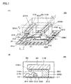
- FIG. 7A is a perspective view showing the inside of the DC-DC converter 200 through the sealing resin layer 204 in the DC-DC converter 200 described in Patent Document 1.
- FIG. 7B is a cross-sectional view of the DC-DC converter 200 shown in FIG.
- the DC-DC converter 200 includes two conductive columns 203A and 203B on a substrate 201.
- the conductive support 203A includes a horizontal portion 203AH and a vertical portion 203AV, and has an inverted L shape.
- the conductive support 203B includes a horizontal portion 203BH and a vertical portion 203BV, and has an inverted L shape in the same manner.
- the substrate 201 is divided into a first portion 201A, a second portion 201B, a third portion 201C, and a fourth portion 201D having an arbitrary planar shape for each electronic component to be mounted.
- the vertical portion 203AV is provided on the third portion 201C.
- the vertical portion 203BV is provided on the fourth portion 201D.
- an inductor 205 that occupies a large area when mounted on the substrate 201 is disposed so as to straddle the horizontal portions 203AH and 203BH.
- the inductor 205 includes external electrodes 213A and 213B.
- the external electrode 213A is connected to the horizontal portion 203AH.
- the external electrode 213B is connected to the horizontal portion 203BH.
- An electronic component 202A such as a switching element is disposed on the first portion 201A and below the horizontal portion 203AH.
- An electronic component 202B such as a capacitor and a resistor is disposed on the second portion 201B and below the horizontal portion 203BH.
- the electronic components 202A and 202B are connected to each other or the peripheral electrode 210 of the substrate 201 by wire bonding 214A and 214B.
- the above components of the DC-DC converter 200 are sealed on the substrate 201 by a sealing resin layer 204.
- an inductor 205 having a large occupied area on the substrate 201 is disposed above the substrate 201, and a laminated structure capable of ensuring the degree of freedom of the arrangement of the electronic components 202A and 202B on the substrate 201. It is said. Therefore, there is an advantage that the DC-DC converter 200 can be reduced in size (reduction in mounting area).
- the inductor 205 is connected to the conductive columns 203A and 203B, and then sealed in the sealing resin layer 204.
- the inductor 205 having a large volume receives a large flow pressure during resin sealing. Therefore, the conductive columns 203A and 203B need to be firmly joined to the substrate 201 so that the inductor 205 does not fall down even when the inductor 205 receives a large flow pressure.
- the inductance of the inductor 205 is also correspondingly reduced. Therefore, in order to transmit constant power, it is necessary to increase the oscillation frequency. was there. In that case, there is a possibility that the switching loss in the switching element becomes large and the power conversion efficiency of the DC-DC converter is lowered.
- an object of the present invention is to provide a DC-DC converter having a small mounting area and high power conversion efficiency.
- the DC-DC converter according to the present invention includes a substrate, a switching element, a conductive support, a sealing resin layer, and an inductor.
- the substrate is provided with a first electrode and a second electrode on one main surface.
- the switching element is disposed on one main surface of the substrate and connected to the first electrode.
- the conductive support column is disposed on one main surface of the substrate, and one end thereof is connected to the second electrode.
- the sealing resin layer is provided on one main surface of the substrate so as to seal the switching element and the conductive column with the other end of the conductive column exposed.
- the inductor is disposed on the conductive support in a state exposed from the sealing resin layer, and is connected to the other end of the conductive support.
- the conductive support is sealed with the other end exposed from the sealing resin layer, and the inductor is disposed on the conductive support with the sealing resin layer exposed.
- the other end of the sex support is connected. That is, the inductor is connected to the conductive support in a stable state surrounded by the sealing resin layer.
- a simple pillar-shaped and thin cross-sectional area can be used as the conductive support. That is, the area occupied by the conductive pillars on the substrate can be reduced. Therefore, the substrate can be reduced, and the mounting area of the DC-DC converter on the motherboard can be reduced.
- the inductor does not receive a flow pressure when sealed with resin, so there is no need to reduce the volume of the inductor. Therefore, the inductance of the inductor is not reduced, and the oscillation frequency can be kept low when transmitting constant power. As a result, the switching loss in the switching element is reduced, and the power conversion efficiency of the DC-DC converter can be increased.
- the DC-DC converter according to the present invention preferably has the following features. That is, when the output current is 50% to 100% of the rated current of the DC-DC converter, the absolute value of the temperature difference between the switching element and the conductive column is 5 ° C. or less. It is arranged on one main surface of the substrate so that
- the rated current of the DC-DC converter can be said to be the maximum current allowed as a steady output current of the DC-DC converter based on the allowable current of the switching element and the electrical resistance of the inductor. In other words, it is different from the definition of the upper limit of the instantaneous large current that flows at the time of start-up, for example, inrush current.
- Switching elements such as field effect transistors (hereinafter sometimes abbreviated as FETs) often used in DC-DC converters generate heat (self-heating) due to switching loss when energized. Therefore, the temperature of the switching element during the operation of the DC-DC converter is obtained by superimposing the above self-heating on the ambient temperature of the DC-DC converter.
- the reliability of a DC-DC converter is often influenced by the failure life of the switching element, and it is important to know the temperature of the switching element during energization, to predict the life and to perform appropriate derating accordingly. Conceivable.
- the switching element is in the sealing resin layer, and its temperature is difficult to measure directly.
- the absolute value of the temperature difference between the switching element and the conductive column is It arrange
- the temperature of the element can be measured indirectly. That is, for example, the life of the DC-DC converter when incorporated in a portable electronic device can be accurately predicted, and the reliability of the DC-DC converter can be improved by performing appropriate derating.
- the preferred embodiment of the DC-DC converter according to the present invention has the following features. That is, the switching element and the conductive column are arranged on one main surface of the substrate so that the distance between the switching element and the conductive column is 1 mm or less.
- the distance between the switching element and the conductive column is 1 mm or less. Therefore, the absolute value of the temperature difference between the switching element and the conductive column is surely 5 ° C. or less. Therefore, the above-described effect can be obtained more reliably.
- the DC-DC converter according to the present invention and various preferred embodiments thereof have the following features. That is, the other end of the conductive support protrudes from the sealing resin layer.
- the other end of the conductive support protrudes from the sealing resin layer. Therefore, when the temperature of the switching element is indirectly measured, it is easy to directly measure the temperature of the conductive support regardless of the temperature of the external electrode of the inductor or the temperature of the connecting member. Therefore, the above-described effect can be obtained more reliably. Needless to say, the mounting area on the mother board can be reduced as in the case of the DC-DC converter according to the present invention.
- the area occupied by the conductive columns on the substrate can be reduced. Therefore, the board can be made small, and the mounting area on the mother board of the DC-DC converter can be made small. Furthermore, in the DC-DC converter according to the present invention, since it is not necessary to reduce the volume of the inductor, the oscillation frequency can be suppressed low. As a result, the switching loss in the switching element is reduced, and the power conversion efficiency of the DC-DC converter can be increased.
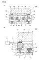
- FIG. 1 is a top view of a DC-DC converter 100 that is a first embodiment of a DC-DC converter according to the present invention, and a cross-sectional view taken along the line AA.
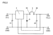
- FIG. 2 is a circuit diagram of the DC-DC converter 100 shown in FIG. 1.
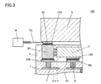
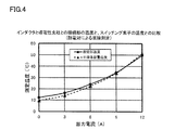
- FIG. 2 is a cross-sectional view schematically showing a method for indirectly measuring the temperature of a switching element 2 in the DC-DC converter 100 shown in FIG. It is the graph which compared and showed the result obtained by the indirect measuring method of the temperature of the switching element 2 shown in FIG. 3, and the result of having measured the temperature of the switching element 2 directly.
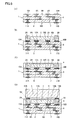
- FIG. 2 is a diagram for explaining an example of a manufacturing method of the DC-DC converter 100 shown in FIG.
- FIG. 1 is a cross-sectional view of a DC-DC converter 100A that is a second embodiment of the DC-DC converter according to the present invention, and a cross-sectional view schematically showing a method for measuring the temperature of the switching element 2 in the DC-DC converter 100A. is there.
- FIG. 4 is a perspective view showing the inside of a DC-DC converter 200 of the background art through a sealing resin layer 204, and is a cross-sectional view taken along the line II-II.
- FIG. 1A is a top view of the DC-DC converter 100.
- 1B is a cross-sectional view of the DC-DC converter 100 taken along the line AA shown in FIG. 1A (shown by a one-dot chain line).
- FIG. 2 is an example of a circuit diagram when the DC-DC converter 100 shown in FIG. 1 is a chopper step-down DC-DC converter.
- the DC-DC converter 100 includes a substrate 1, a switching element 2, conductive columns 3 ⁇ / b> A and 3 ⁇ / b> B, a sealing resin layer 4, and an inductor 5.
- the substrate 1 is a ceramic multilayer substrate having a ceramic layer 6 and an internal conductor including a pattern conductor 7 and a via conductor 8.
- the ceramic layer 6 includes a ceramic material that is, for example, a Ba—Al—Si-based oxide.
- the inner conductor is formed using, for example, Cu.
- the first main surface M1 of the substrate 1 is provided with the first electrodes 9A and 9B and the second electrodes 10A and 10B, and the other main surface M2 is provided with the third electrodes 11A and 11B.
- the first electrode 9A and the second electrode 10A have the same potential
- the first electrode 9B and the second electrode 10B have the same potential by a wiring (not shown). Connected to be.
- the first to third electrodes are formed using, for example, Cu.
- the first to third electrodes may have a Cu layer as a base and a plating layer such as Ni or Sn formed on the surface thereof.
- a dotted line is attached to the inside of the substrate 1, which indicates that the substrate 1 is obtained by laminating and sintering ceramic green sheets. It does not indicate that such an interface is present in 1.
- the switching element 2 is preferably an FET, for example.
- the switching element 2 is disposed on one main surface M1 of the substrate 1, one of its external electrodes 12A is connected to one 9A of the first electrode, and the other 12B of the external electrode is the other 9B of the first electrode. Connected with.
- the connection between the external electrodes 12A and 12B of the switching element 2 and the first electrodes 9A and 9B is performed using a first connecting member S1 such as solder.
- the conductive support pillars 3A and 3B are disposed on the one main surface M1 of the substrate 1, and one end of the conductive support pillar 3A is connected to the second electrode 10A and the other of the conductive support pillars 3B. One end is connected to the other 10B of the second electrode.
- the conductive struts 3A and 3B are preferably made of a metal material having a small specific heat and a high thermal conductivity, such as Cu and Ag.
- the sealing resin layer 4 is seen through to show the switching element 2 and the conductive columns 3A and 3B (illustrated by dotted lines).
- the connection between the conductive columns 3A and 3B and the second electrodes 10A and 10B is also performed using a first connection member S1 such as solder.
- the switching element 2 and the conductive pillars 3A, 3B are arranged on one main surface M1 of the substrate 1 so that the distance between both the switching element 2 and the conductive pillars 3A, 3B is 1 mm or less. Is arranged.
- the conductive columns 3A and 3B may be arranged so that the distance between at least one of them and the switching element 2 is 1 mm or less. The same applies to the case where the number of conductive columns is three or more.
- the sealing resin layer 4 is provided on one main surface M1 of the substrate 1 so as to seal the switching element 2 and the conductive columns 3A and 3B with the other ends of the conductive columns 3A and 3B exposed. It has been.
- the sealing resin layer 4 is an insulating resin material or a material in which, for example, a glass material or silica is dispersed as a filler in an insulating resin material. A single insulating resin material that does not include a filler may be used.
- the inductor 5 is a so-called choke coil.
- the inductor 5 is disposed on the conductive pillars 3A and 3B in a state exposed from the sealing resin layer 4, and one of the external electrodes 13A is connected to the other end of the conductive pillar one 3A and the other of the external electrodes 13B is connected to the other end of the other 3B of the conductive column.
- the main components of the DC-DC converter 100 have been described above, but the other components are as shown in the circuit diagram of FIG.
- the diode D is mounted on the substrate 1 and is sealed by the sealing resin layer 4 together with the switching element 2 and the conductive pillars 3A and 3B.
- Capacitors C1 and C2 can be formed in a predetermined number and arrangement in the substrate 1 by appropriately setting the area and material of the pattern conductor 7 and the arrangement of the ceramic layer 6 and the via conductor 8 (see FIG. 1 (not shown).
- separately prepared capacitors C 1 and C 2 and diode D may be mounted on substrate 1 and sealed with sealing resin layer 4.
- the conductive columns 3A and 3B are sealed with the other ends exposed from the sealing resin layer 4.
- the inductor 5 is arrange
- the conductive columns 3A and 3B do not need to have a large cross-sectional area in consideration of the flow pressure to the inductor 5, and are simple columnar. Those having a small cross-sectional area can be used. That is, the area occupied by the conductive columns 3A and 3B on the substrate 1 can be reduced. As a result, a DC-DC converter having a small mounting area on the motherboard can be obtained.
- the conductive support pillars 3A and 3B are in a stable state surrounded by the sealing resin layer 4, and do not fall down even if the volume of the inductor 5 to be connected is increased. As a result, since the oscillation frequency can be kept low, switching loss in the switching element can be suppressed. As a result, a DC-DC converter with high power conversion efficiency can be obtained.
- FIG. 3 is a cross-sectional view schematically showing an indirect method for measuring the temperature of the switching element 2 in the DC-DC converter 100 shown in FIG.
- the switching element 2 and the conductive support 3A are arranged such that the distance d between them is 1 mm or less.
- FIG. 4 is a graph comparing the result obtained by the measurement method of FIG. 3 with the result of directly measuring the temperature of the switching element 2. In the temperature measurement shown in FIG. 4, the above-described DC-DC converter having a rated current of 12 A was used as the switching element 2.
- one end 13 ⁇ / b> A of the external electrode is connected by bringing the tip of the thermocouple TC connected to the measuring device M into contact with one side 13 ⁇ / b> A of the external electrode of the inductor 5.
- the temperature of one side 3A of the conductive support was measured.
- the temperature measurement is not limited to contact measurement using a thermocouple, but may be non-contact measurement such as a radiation thermometer.
- the temperature of the conductive support 3 ⁇ / b> A is increased by receiving heat T transmitted from the switching element 2 through the sealing resin layer 4 and the internal conductor. Further, in order to directly measure the temperature of the switching element 2, a sample having a small hole formed on the upper surface of the sealing resin layer 4 was produced so that the switching element 2 was exposed. Then, the temperature of the switching element 2 was measured directly by bringing the tip of the thermocouple into contact with the exposed switching element 2. By this measurement, the difference between the temperature of the conductive support 3A and the temperature of the switching element 2 was examined.
- FIG. 4 showing the result shows that the temperature of the connection portion (the temperature of one of the external electrodes 13A of the inductor 5 and the temperature of the one of the conductive support 3A) over the entire output current, and switching
- the absolute value of the temperature difference from the temperature of the element 2 is 5 ° C. or less.
- the output current is 6 A to 12 A, that is, when the output current is 50% or more and 100% or less of the rated current value of the DC-DC converter, the difference is further reduced, which is preferable.
- the absolute value of the temperature difference is 5 ° C. or less, the lifetime of the DC-DC converter when incorporated in a portable electronic device, for example, can be accurately predicted with sufficient practical accuracy. Further, the reliability of the DC-DC converter can be improved by performing appropriate derating based on the result.
- the absolute value of the temperature difference is 5 ° C. or less over the entire output current.
- the absolute value of the temperature difference sometimes exceeded 5 ° C. when it was less than 50% of the rated current value.
- the absolute value of the temperature difference was 5 ° C. or less at 50% to 100% of the rated current. Therefore, the temperature difference between the connection portion temperature and the temperature of the switching element 2 is discussed from 50% to 100% of the rated current.
- the temperature is measured by bringing the tip of the thermocouple TC into contact with one of the external electrodes 13A of the inductor 5, but it may be measured by bringing it into contact with the connecting member S2. Good.
- FIG. 5A schematically shows a substrate preparation step in the method of manufacturing the DC-DC converter 100, and is a cross-sectional view corresponding to the cross-sectional view taken along the arrow in FIG. 1B (hereinafter, FIG. The same applies to (D).
- the substrate preparation step in this embodiment the substrate 1 is prepared as an individual piece, but an assembly of the substrates 1 may be prepared. After the inductor connection process described later is completed, the assembly of the substrates 1 may be cut into pieces.
- a ceramic green sheet is produced using ceramic material powder.
- an electrode pattern to be the pattern conductor 7 and the via conductor 8 is formed on the ceramic green sheet using a conductor paste and a resistance paste.
- a ceramic green sheet including the electrode pattern is laminated and pressure-bonded so that an internal conductor having a predetermined path is formed.
- an electrode pattern to be the first electrodes 9A and 9B and the second electrodes 10A and 10B is formed on one main surface of the laminate using a conductor paste.
- an electrode pattern to be the third electrodes 11A and 11B is similarly formed on the other main surface of the multilayer body.
- substrate 1 is produced by baking a laminated body.
- FIG. 5B is a cross-sectional view schematically showing a switching element and conductive support connecting step in the method of manufacturing the DC-DC converter 100. This step may be performed on the aggregate of the substrates 1 as described above.
- one of the external electrodes 12A of the switching element 2 is connected to one 9A of the first electrode, and the other 12B of the external electrode is connected to the other 9B of the first electrode.
- one end of one of the conductive columns 3A is connected to one 10A of the second electrode, and one end of the other 3B of the conductive column is connected to the other 10B of the second electrode.
- These connections are made by applying a solder paste serving as the connection member S1 to the first electrodes 9A and 9B and the second electrodes 10A and 10B on the one main surface M1 of the substrate 1, and switching elements 2 and conductive columns 3A. After arranging 3B, it can be performed by performing reflow heating.
- the solder paste can be applied by screen printing, for example.
- FIG. 5C is a cross-sectional view schematically showing a sealing resin layer forming step in the method for manufacturing the DC-DC converter 100. This step may be performed on the aggregate of the substrates 1 as described above.
- the sealing resin layer 4 is provided on the one main surface M1 of the substrate 1 so as to seal the switching element 2 and the conductive columns 3A and 3B. At this time, the other ends of the conductive columns 3A and 3B are exposed.
- the sealing resin layer 4 may be formed so that the other ends of the conductive columns 3A and 3B are exposed from the beginning, and the other ends of the conductive columns 3A and 3B are temporarily connected to the sealing resin layer 4. After being buried in, the other ends of the conductive columns 3A and 3B may be exposed by grinding.
- FIG. 5D is a cross-sectional view schematically showing an inductor connection step in the method for manufacturing the DC-DC converter 100. This step may be performed on the aggregate of the substrates 1 as described above. And after this process is complete
- FIG. 5D is a cross-sectional view schematically showing an inductor connection step in the method for manufacturing the DC-DC converter 100. This step may be performed on the aggregate of the substrates 1 as described above. And after this process is complete
- one of the external electrodes 13A of the inductor 5 is connected to the other end of the conductive column 3A, and the other 13B of the external electrode is connected to the other end of the conductive column 3B. That is, the inductor 5 is disposed on the conductive support columns 3A and 3B in a state of being exposed from the sealing resin layer 4.
- This connection can be performed by applying a solder paste to be the connection member S2 to the other end of one of the conductive pillars 3A and the other end of the other 3B, placing the inductor 5, and then performing reflow heating. Also, as described above, the solder paste can be applied by, for example, screen printing.
- the connecting member S1 and the connecting member S2 described above may be made of different materials or the same material.
- the melting point of the material of the connecting member S1 is preferably higher than the melting point of the material of the connecting member S2. In that case, there is no possibility that the connecting member S1 is remelted by reflow in the inductor connecting step.
- the DC-DC converter 100 according to the present invention can be efficiently manufactured.
- the DC-DC converter 100A which is a second embodiment of the DC-DC converter according to the present invention will be described with reference to FIG.
- the DC-DC converter 100A has basically the same structure as the DC-DC converter 100 shown in FIG. 1, but is characterized by the state of the ends of the conductive columns 3A and 3B. Description of other parts common to the DC-DC converter 100 is omitted.
- FIG. 6A is a cross-sectional view of a DC-DC converter 100A which is a second embodiment of the DC-DC converter according to the present invention.
- the other ends of the conductive columns 3A and 3B protrude from the sealing resin layer.
- the protruding distance There is no particular limitation on the protruding distance.
- FIG. 6B when the temperature of the switching element 2 is indirectly measured, it depends on the measurement of the temperature of the external electrode 13A of the inductor 5 or the connection member S2 described in the first embodiment. Instead, the temperature of the conductive support 3A can be directly measured.
- the life of a DC-DC converter when incorporated in a portable electronic device can be predicted with higher accuracy. Further, by performing appropriate derating based on the result, the reliability of the DC-DC converter can be further improved.
- this invention is not limited to said embodiment, A various application and deformation
- the shape and number of conductive columns can be changed as appropriate in accordance with the mechanism and shape of the DC-DC converter.
- the ceramic multilayer substrate is used as the substrate, but the type of the multilayer substrate is not particularly limited.
- a single layer substrate other than a multilayer substrate for example, a resin composite material such as a so-called glass epoxy substrate may be used.
- Other components of the DC-DC converter can be appropriately changed in accordance with the mechanism and shape of the DC-DC converter.
- the present invention has been described by taking a chopper step-down DC-DC converter as an example, but a step-up DC-DC converter or a step-up / step-down DC-DC converter of the same type may be used. Further, other types (eg, insulation type) of DC-DC converters may be used.
- a DC-DC converter with a small mounting area and high power conversion efficiency can be provided.
- 100 DC-DC converter 1 substrate, 2 switching element, 3A, 3B conductive support, 4 sealing resin layer, 5 inductor, 6 ceramic layer, 7 pattern conductor (internal conductor), 8 via conductor (internal conductor), 9A , 9B first electrode, 10A, 10B second electrode, 11A, 11B third electrode, 12A, 12B switching element external electrode, 13A, 13B inductor external electrode, one main surface of M1 substrate, M2 substrate The other main surface, S1 first connecting member, S2 second connecting member.
Landscapes
- Engineering & Computer Science (AREA)
- Power Engineering (AREA)
- Dc-Dc Converters (AREA)
Abstract
DC-DCコンバータ(100)は、基板(1)と、スイッチング素子(2)と、導電性支柱(3A、3B)と、封止樹脂層(4)と、インダクタ(5)とを備える。基板(1)は、一方主面(M1)に第1の電極(9A、9B)および第2の電極(9C、9D)が設けられている。スイッチング素子(2)は、基板(1)上に配置され、第1の電極(9A、9B)と接続されている。導電性支柱(3A、3B)は、基板(1)上に配置され、一端が第2の電極(9C、9D)と接続されている。封止樹脂層(4)は、基板(1)の一方主面上に、スイッチング素子(2)および導電性支柱(3A、3B)を、導電性支柱(3A、3B)の他端が露出した状態で封止するように設けられている。インダクタ(5)は、導電性支柱(3A、3B)上に封止樹脂層(4)から露出した状態で配置され、かつ導電性支柱(3A、3B)の他端と接続されている。
Description
この発明は、インダクタおよびスイッチング素子などの電子部品が基板に実装されてなるDC-DCコンバータに関するものである。
携帯型電子機器など、近年の電子機器は、小型化に伴いマザーボードの面積が小さくなっており、その一方で、高機能化に伴いマザーボードに実装される電子部品および電子部品モジュールの数が増加している。そのため、電子部品および電子部品モジュールは、マザーボード上における実装面積(実装時におけるマザーボード上での占有面積)を小さくすることが要求されている。
一の直流電圧を他の直流電圧に変換するDC-DCコンバータは、インダクタおよびスイッチング素子などの電子部品が基板に実装されてなる電子部品モジュールの1つである。DC-DCコンバータを構成するインダクタは、スイッチング素子におけるスイッチング損失を小さくし、DC-DCコンバータの電力変換効率を向上させるため、発振周波数を低くすることが好ましい。その場合、インダクタの体積は大きくなり、他の電子部品より実装面積が大きくなる。したがって、インダクタおよびスイッチング素子などの電子部品を2次元的に基板に実装すると、大きな基板が必要になる。その結果、DC-DCコンバータの実装面積が大きくなるという問題がある。
DC-DCコンバータの実装面積を小さくする方法の一つとして、DC-DCコンバータの構成要素を、3次元的に基板に実装することが考えられる。特開2015-73011号公報(特許文献1)にはそのようなDC-DCコンバータの一例が提案されている。
図7(A)は、特許文献1に記載されているDC-DCコンバータ200において、封止樹脂層204を透視して、DC-DCコンバータ200の内部を示した透視斜視図である。図7(B)は、図7(A)に示したDC-DCコンバータ200の、II-II線を含む面の矢視断面図である。
図7(A)、(B)に示すように、DC-DCコンバータ200は、基板201上に、2本の導電性支柱203A、203Bを備えている。導電性支柱203Aは、水平部分203AHと垂直部分203AVとを含んでおり、逆L字状となっている。また、導電性支柱203Bは、水平部分203BHと垂直部分203BVとを含んでおり、同様に逆L字状となっている。
この例では、基板201は、搭載される電子部品ごとに任意の平面形状を有する第1部分201A、第2部分201B、第3部分201Cおよび第4部分201Dに分割されている。垂直部分203AVは、第3部分201C上に設けられている。また、垂直部分203BVは、第4部分201D上に設けられている。
導電性支柱203A、203B上には、基板201上に実装した場合、その占有面積が大きくなるインダクタ205が、水平部分203AH、203BHに跨るように配置されている。インダクタ205は外部電極213A、213Bを備えている。外部電極213Aは、水平部分203AHと接続されている。また、外部電極213Bは、水平部分203BHと接続されている。
第1部分201A上であって、水平部分203AHの下方領域には、例えばスイッチング素子のような電子部品202Aが配置されている。また、第2部分201B上であって、水平部分203BHの下方領域には、例えばコンデンサや抵抗のような電子部品202Bが配置されている。電子部品202A、202Bは、ワイヤボンディング214A、214Bなどにより、電子部品相互または基板201の周辺電極210と接続されている。以上のDC-DCコンバータ200の構成要素は、封止樹脂層204によって、基板201上に封止されている。
このようなDC-DCコンバータ200は、基板201上での占有面積が大きくなるインダクタ205を基板201の上方に配置し、基板201上の電子部品202A、202Bの配置の自由度を確保できる積層構造としている。そのため、DC-DCコンバータ200の小型化(実装面積の低減)が可能となるという利点を有する。
上記のDC-DCコンバータ200は、インダクタ205を導電性支柱203A、203Bと接続した後、封止樹脂層204内に封止している。構成要素の中でも体積の大きなインダクタ205は、樹脂封止時に大きな流動圧力を受ける。したがって、導電性支柱203A、203Bは、インダクタ205が大きな流動圧力を受けても倒れることがないように、基板201と強固に接合される必要がある。そのためには、垂直部分203AV、203BVの断面積を大きくする必要がある(図7(B)参照)。すなわち、基板201上において垂直部分203AV、203BVが占有する面積はいまだに大きく、DC-DCコンバータ200の実装面積の低減は不十分なものに止まっていた。
一方、樹脂封止時に大きな流動圧力を受けないように、インダクタ205の体積を小さくすると、その分インダクタ205のインダクタンスも小さくなるため、一定の電力を伝送するためには、発振周波数を高くする必要があった。その場合、スイッチング素子におけるスイッチング損失が大きくなり、DC-DCコンバータの電力変換効率が低下する虞がある。
そこで、この発明の目的は、実装面積が小さく、かつ電力変換効率が高いDC-DCコンバータを提供することである。
この発明では、実装面積が小さく、電力変換効率が高いDC-DCコンバータを得るため、DC-DCコンバータの構成要素であるインダクタの実装形態についての改良が図られる。
この発明に係るDC-DCコンバータは、基板と、スイッチング素子と、導電性支柱と、封止樹脂層と、インダクタと、を備える。基板は、一方主面に第1の電極および第2の電極が設けられている。スイッチング素子は、基板の一方主面上に配置され、第1の電極と接続されている。導電性支柱は、基板の一方主面上に配置され、一端が第2の電極と接続されている。封止樹脂層は、基板の一方主面上に、スイッチング素子および導電性支柱を導電性支柱の他端が露出した状態で封止するように設けられている。インダクタは、導電性支柱上に封止樹脂層から露出した状態で配置され、導電性支柱の他端と接続されている。
上記のDC-DCコンバータでは、導電性支柱は、その他端が封止樹脂層から露出した状態で封止され、インダクタは、導電性支柱上に封止樹脂層から露出した状態で配置され、導電性支柱の他端と接続されている。すなわち、インダクタは、封止樹脂層によって周囲を囲まれて安定した状態にある導電性支柱と接続されている。この場合、インダクタは、樹脂封止時に流動圧力を受けないため、導電性支柱としては、単純な柱状の、断面積の細いものを用いることができる。すなわち、基板上における導電性支柱の占有する面積を小さくすることができる。したがって、基板を小さくすることができ、延いてはDC-DCコンバータのマザーボード上における実装面積を小さくすることができる。
さらに、上記のDC-DCコンバータでは、インダクタが樹脂封止時に流動圧力を受けないため、インダクタの体積を小さくする必要がない。したがって、インダクタのインダクタンスが小さくならず、一定の電力を伝送する際に、発振周波数を低く抑えることができる。その結果、スイッチング素子におけるスイッチング損失が小さくなり、DC-DCコンバータの電力変換効率を高くすることができる。
この発明に係るDC-DCコンバータは、以下の特徴を備えることが好ましい。すなわち、スイッチング素子および導電性支柱は、出力電流をDC-DCコンバータの定格電流の50%以上100%以下とした場合、スイッチング素子と導電性支柱との間の温度差の絶対値が5℃以下となるように、基板の一方主面上に配置されている。
ここで、DC-DCコンバータの定格電流とは、スイッチング素子の許容電流およびインダクタの電気抵抗などに基づき、DC-DCコンバータの定常的な出力電流として許容される最大電流ということができる。すなわち、例えば突入電流のような、始動時に流れる瞬間的な大電流の上限の規定とは異なるものである。
DC-DCコンバータに用いられることの多い電界効果トランジスタ(以下、FETと略称することがある)のようなスイッチング素子は、通電時にスイッチング損失などにより発熱(自己発熱)する。そのため、DC-DCコンバータの動作時のスイッチング素子の温度は、DC-DCコンバータの周囲温度に上記の自己発熱が重畳したものとなる。DC-DCコンバータの信頼性は、スイッチング素子の故障寿命に影響されることが多く、通電時のスイッチング素子の温度を把握し、寿命予測およびそれに伴う適切なディレーティングを行なうことは重要であると考えられる。
しかしながら、スイッチング素子は、封止樹脂層内にあり、直接にはその温度を測定し難い。一方、上記のDC-DCコンバータでは、スイッチング素子および導電性支柱は、通常の動作範囲である出力電流が定格電流の50%以上100%以下とした場合、両者の間の温度差の絶対値が5℃以下となるように、基板の一方主面上に配置されている。したがって、導電性支柱、導電性支柱に接続されているインダクタの外部電極、または導電性支柱とインダクタの外部電極とを接続する接続部材の温度を測定することにより、実用上十分な精度で、スイッチング素子の温度を間接的に測定することができる。すなわち、例えば携帯型電子機器に組み込まれた際のDC-DCコンバータの寿命を精度良く予測でき、また適切なディレーティングを行なうことにより、DC-DCコンバータの信頼性を向上させることができる。
この発明に係るDC-DCコンバータの好ましい実施形態は、以下の特徴を備えることがさらに好ましい。すなわち、スイッチング素子および導電性支柱は、スイッチング素子と導電性支柱との間の距離が1mm以下となるように、基板の一方主面上に配置されている。
上記のDC-DCコンバータでは、スイッチング素子と導電性支柱との間の距離が1mm以下となっている。したがって、スイッチング素子と導電性支柱との間の温度差の絶対値が、確実に5℃以下となる。そのため、前述の効果をさらに確実に得ることができる。
この発明に係るDC-DCコンバータおよびその好ましい種々の実施形態は、以下の特徴を備えることがさらに好ましい。すなわち、導電性支柱の他端は、封止樹脂層から突出している。
上記のDC-DCコンバータでは、導電性支柱の他端は、封止樹脂層から突出している。したがって、スイッチング素子の温度を間接的に測定するにあたり、インダクタの外部電極または接続部材の温度の測定に依らず、導電性支柱の温度を直接測定し易くなっている。そのため、前述の効果をさらに確実に得ることができる。また、この発明に係るDC-DCコンバータと同様に、マザーボード上における実装面積を小さくすることができるという効果が得られることは言うまでもない。
この発明に係るDC-DCコンバータでは、基板上における導電性支柱の占有する面積を小さくすることができる。したがって、基板を小さくすることができ、DC-DCコンバータのマザーボード上における実装面積を小さくすることができる。さらに、この発明に係るDC-DCコンバータでは、インダクタの体積を小さくする必要がないため、発振周波数を低く抑えることができる。その結果、スイッチング素子におけるスイッチング損失が小さくなり、DC-DCコンバータの電力変換効率を高くすることができる。
以下にこの発明の実施形態を示して、この発明の特徴とするところをさらに詳しく説明する。
-DC-DCコンバータの第1の実施形態-
この発明に係るDC-DCコンバータの第1の実施形態であるDC-DCコンバータ100について、図1および図2を用いて説明する。
この発明に係るDC-DCコンバータの第1の実施形態であるDC-DCコンバータ100について、図1および図2を用いて説明する。
<DC-DCコンバータの構造>
図1(A)は、DC-DCコンバータ100の上面図である。図1(B)は、DC-DCコンバータ100の、図1(A)に示したA-A線を含む面(一点鎖線により図示)の矢視断面図である。また、図2は、図1に示したDC-DCコンバータ100を、チョッパ方式の降圧型DC-DCコンバータとした場合の回路図の一例である。
図1(A)は、DC-DCコンバータ100の上面図である。図1(B)は、DC-DCコンバータ100の、図1(A)に示したA-A線を含む面(一点鎖線により図示)の矢視断面図である。また、図2は、図1に示したDC-DCコンバータ100を、チョッパ方式の降圧型DC-DCコンバータとした場合の回路図の一例である。
DC-DCコンバータ100は、基板1と、スイッチング素子2と、導電性支柱3A、3Bと、封止樹脂層4と、インダクタ5と、を備える。
この実施形態において、基板1は、セラミック層6と、パターン導体7およびビア導体8を含む内部導体とを有するセラミック多層基板である。セラミック層6は、例えばBa-Al-Si系酸化物であるセラミック材料を含んでなる。内部導体は、例えばCuを用いて形成される。また、基板1の一方主面M1には、第1の電極9A、9Bおよび第2の電極10A、10Bが設けられ、他方主面M2には、第3の電極11A、11Bが設けられている。なお、この実施形態では、不図示の配線により、第1の電極9Aと第2の電極10Aとが同電位となるように、および第1の電極9Bと第2の電極10Bとが同電位となるように接続されている。第1ないし第3の電極は、例えばCuを用いて形成される。なお、第1ないし第3の電極は、Cu層を下地とし、その表面にNi、Snなどのめっき層を形成するようにしてもよい。
なお、図1(B)では基板1の内部に点線が付されているが、これは基板1がセラミックグリーンシートを積層して焼結させたものであることを示すものであり、実際の基板1中にこのような界面があることを示すものではない。
スイッチング素子2は、例えばFETなどが好ましく用いられる。スイッチング素子2は、基板1の一方主面M1上に配置され、その外部電極の一方12Aは、第1の電極の一方9Aと接続され、外部電極の他方12Bは、第1の電極の他方9Bと接続されている。スイッチング素子2の外部電極の12A、12Bと第1の電極9A、9Bとの接続は、例えばはんだのような第1の接続部材S1を用いて行なわれている。
導電性支柱3A、3Bは、同様に基板1の一方主面M1上に配置され、導電性支柱の一方3Aの一端は、第2の電極の一方10Aと接続され、導電性支柱の他方3Bの一端は、第2の電極の他方10Bと接続されている。導電性支柱3A、3Bは、比熱が小さく、かつ熱伝導率の高い、例えばCuおよびAgのような金属材料が好ましく用いられる。なお、図1(A)では、封止樹脂層4を透視して、スイッチング素子2および導電性支柱3A、3Bを示している(点線により図示)。導電性支柱3A、3Bと第2の電極10A、10Bとの接続も、スイッチング素子2の場合と同様に、例えばはんだのような第1の接続部材S1を用いて行なわれている。
この実施例において、スイッチング素子2および導電性支柱3A、3Bは、スイッチング素子2と導電性支柱3A、3Bの両方との間の距離が1mm以下となるように、基板1の一方主面M1上に配置されている。なお、導電性支柱3A、3Bは、その少なくとも一方と、スイッチング素子2との間の距離が1mm以下となるように配置されていればよい。このことは、導電性支柱の数が3本以上の場合も同様である。
封止樹脂層4は、基板1の一方主面M1上に、スイッチング素子2および導電性支柱3A、3Bを、導電性支柱3A、3Bの他端がそれぞれ露出した状態で封止するように設けられている。封止樹脂層4は、絶縁性の樹脂材料、または絶縁性の樹脂材料中にフィラーとして例えばガラス材料やシリカなどを分散させたものである。なお、フィラーを含まない、単一の絶縁性の樹脂材料であってもよい。
インダクタ5は、いわゆるチョークコイルと呼ばれるものである。インダクタ5は、導電性支柱3A、3B上に封止樹脂層4から露出した状態で配置され、その外部電極の一方13Aは、導電性支柱の一方3Aの他端と接続され、外部電極の他方13Bは、導電性支柱の他方3Bの他端と接続されている。
なお、DC-DCコンバータ100の主要な構成要素については、以上で説明したが、それ以外の構成要素については、図2の回路図に示されている通りである。ダイオードDは、基板1上に実装されており、スイッチング素子2および導電性支柱3A、3Bと共に、封止樹脂層4により封止されている。コンデンサC1、C2は、パターン導体7の面積および材質と、セラミック層6およびビア導体8の配置とを適宜設定することにより、基板1の内部に所定の個数および配置で作り込むことができる(図1には不図示)。また、別に用意されたコンデンサC1、C2およびダイオードDを基板1上に実装し、封止樹脂層4により封止するようにしてもよい。
上記のDC-DCコンバータ100では、導電性支柱3A、3Bは、その他端が封止樹脂層4から露出した状態で封止されている。そして、インダクタ5は、導電性支柱3A、3B上に封止樹脂層4から露出した状態で配置され、導電性支柱3A、3Bの他端と接続されている。すなわち、インダクタ5は、封止樹脂層4によって周囲を囲まれて安定した状態にある導電性支柱3A、3Bと接続されている。
この場合、インダクタ5は、樹脂封止時に流動圧力を受けないため、導電性支柱3A、3Bとしては、インダクタ5への流動圧力まで考慮して、断面積を大きくする必要がなくなり、単純な柱状の、断面積の細いものを用いることができる。すなわち、基板1上における導電性支柱3A、3Bの占有する面積を小さくすることができる。その結果、マザーボード上における実装面積の小さいDC-DCコンバータが得られる。
さらに、導電性支柱3A、3Bは、封止樹脂層4によって周囲を囲まれて安定した状態にあり、接続されるインダクタ5の体積を大きくしても倒れることがない。その結果、発振周波数を低く維持できるため、スイッチング素子におけるスイッチング損失を抑えることができる。その結果、電力変換効率の高いDC-DCコンバータが得られる。
<スイッチング素子の温度測定>
図1に示したDC-DCコンバータ100におけるスイッチング素子2の温度の間接的な測定方法について、図3および図4を用いて説明する。
図1に示したDC-DCコンバータ100におけるスイッチング素子2の温度の間接的な測定方法について、図3および図4を用いて説明する。
図3は、図1に示したDC-DCコンバータ100における、スイッチング素子2の温度の間接的な測定方法を模式的に示した断面図である。前述のように、スイッチング素子2および導電性支柱3Aは、両者の間の距離dが1mm以下となるように配置されている。また、図4は、図3の測定方法により得られた結果と、スイッチング素子2の温度を直に測定した結果とを比較して示したグラフである。なお、図4に示した温度測定には、スイッチング素子2として、前述の定格電流が12AであるDC-DCコンバータを用いた。
この実施形態では、図3に示すように、測定装置Mに接続された熱電対TCの先端をインダクタ5の外部電極の一方13Aに当接させることにより、外部電極の一方13Aが接続されている導電性支柱の一方3Aの温度を測定した。なお、温度の測定は、熱電対による接触測定に限らず、例えば放射温度計のような非接触測定でもよい。
導電性支柱3Aは、スイッチング素子2から封止樹脂層4や内部導体を介して伝わる熱Tを受けて温度が上昇する。また、スイッチング素子2の温度を直に測定するため、スイッチング素子2が露出するように、封止樹脂層4の上面に小孔を開けたサンプルを作製した。そして、露出したスイッチング素子2に熱電対の先端を当接させることにより、スイッチング素子2の温度を直に測定した。この測定により、導電性支柱3Aの温度と、スイッチング素子2の温度との差を調べた。
その結果を示した図4を見ると、出力電流の全域に亘って、接続部温度(インダクタ5の外部電極の一方13Aの温度で、実質的に導電性支柱の一方3Aの温度)と、スイッチング素子2の温度との間の温度差の絶対値は、5℃以下となっている。特に、出力電流が6Aから12A、すなわち出力電流をDC-DCコンバータの定格電流値の50%以上100%以下とした場合、その差はさらに小さくなっており好ましい。実際には、温度差の絶対値が5℃以下であれば、実用上十分な精度で、例えば携帯型電子機器に組み込まれた際のDC-DCコンバータの寿命を精度良く予測できる。また、その結果に基づいて、適切なディレーティングを行なうことにより、DC-DCコンバータの信頼性を向上させることができる。
なお、図4のグラフでは、出力電流の全域に亘って、温度差の絶対値は5℃以下となっている。一方、定格電流の異なる別のDC-DCコンバータのスイッチング素子2の温度測定においては、定格電流値の50%未満では、温度差の絶対値が5℃を超える場合もあった。しかしながら、その場合でも、定格電流の50%以上100%以下では、温度差の絶対値は5℃以下となっていた。そのため、接続部温度とスイッチング素子2の温度との間の温度差については、定格電流の50%以上から100%以下で議論するものとした。また、この実験例では、前述のように熱電対TCの先端をインダクタ5の外部電極の一方13Aに当接させて温度を測定しているが、接続部材S2に当接させて測定してもよい。
<DC-DCコンバータの製造方法>
図1に示したDC-DCコンバータ100の製造方法の一例について、図5を用いて説明する。
図1に示したDC-DCコンバータ100の製造方法の一例について、図5を用いて説明する。
<基板準備工程>
図5(A)は、DC-DCコンバータ100の製造方法における、基板準備工程を模式的に示す、図1(B)の矢視断面図に相当する断面図(以下、図5(B)ないし(D)も同様)である。この実施形態における基板準備工程では、基板1を個片として準備しているが、基板1の集合体を準備してもよい。後述のインダクタ接続工程が終了してから、基板1の集合体を切断して、個片化するようにしてもよい。
図5(A)は、DC-DCコンバータ100の製造方法における、基板準備工程を模式的に示す、図1(B)の矢視断面図に相当する断面図(以下、図5(B)ないし(D)も同様)である。この実施形態における基板準備工程では、基板1を個片として準備しているが、基板1の集合体を準備してもよい。後述のインダクタ接続工程が終了してから、基板1の集合体を切断して、個片化するようにしてもよい。
この工程では、まず、セラミック材料粉末を用いてセラミックグリーンシートを作製する。次に、セラミックグリーンシートにパターン導体7およびビア導体8となる電極パターンを、導体ペーストおよび抵抗ペーストを用いて形成する。そして、所定の経路を有する内部導体が形成されるように、電極パターンが形成されたものを含むセラミックグリーンシートを積層圧着する。さらに、第1の電極9A、9Bおよび第2の電極10A、10Bとなる電極パターンを、導体ペーストを用いて積層体の一方主面上に形成する。さらに、第3の電極11A、11Bとなる電極パターンを、同様にして積層体の他方主面上に形成する。その後、積層体を焼成することにより、基板1を作製する。
<スイッチング素子および導電性支柱接続工程>
図5(B)は、DC-DCコンバータ100の製造方法における、スイッチング素子および導電性支柱接続工程を模式的に示す断面図である。なお、この工程は、前述のように基板1の集合体に対して行なってもよい。
図5(B)は、DC-DCコンバータ100の製造方法における、スイッチング素子および導電性支柱接続工程を模式的に示す断面図である。なお、この工程は、前述のように基板1の集合体に対して行なってもよい。
この工程では、スイッチング素子2の外部電極の一方12Aを第1の電極の一方9Aと接続し、外部電極の他方12Bを第1の電極の他方9Bと接続する。また、導電性支柱の一方3Aの一端を第2の電極の一方10Aと接続し、導電性支柱の他方3Bの一端を第2の電極の他方10Bと接続する。これらの接続は、基板1の一方主面M1上にある第1の電極9A、9Bおよび第2の電極10A、10Bに接続部材S1となるはんだペーストを塗布し、スイッチング素子2および導電性支柱3A、3Bを配置した後、リフロー加熱を行なうことにより行なうことができる。また、はんだペーストの塗布は、例えばスクリーン印刷などにより行なうことができる。
<封止樹脂層形成工程>
図5(C)は、DC-DCコンバータ100の製造方法における、封止樹脂層形成工程を模式的に示す断面図である。なお、この工程は、前述のように基板1の集合体に対して行なってもよい。
図5(C)は、DC-DCコンバータ100の製造方法における、封止樹脂層形成工程を模式的に示す断面図である。なお、この工程は、前述のように基板1の集合体に対して行なってもよい。
この工程では、基板1の一方主面M1上に、スイッチング素子2および導電性支柱3A、3Bを封止するように封止樹脂層4を設ける。その際、導電性支柱3A、3Bの他端が露出した状態とする。この工程により、スイッチング素子2が封止されるのみならず、導電性支柱3A、3Bが封止樹脂層4によって周囲を囲まれて安定した状態とされる。なお、封止樹脂層4は、最初から導電性支柱3A、3Bの他端が露出した状態となるように形成してもよく、一旦導電性支柱3A、3Bの他端を封止樹脂層4に埋没させた後、研削により導電性支柱3A、3Bの他端が露出した状態となるように形成してもよい。
<インダクタ接続工程>
図5(D)は、DC-DCコンバータ100の製造方法における、インダクタ接続工程を模式的に示す断面図である。なお、この工程は、前述のように基板1の集合体に対して行なってもよい。そして、この工程が終了してから、基板1の集合体を切断して、個片化するようにしてもよい。
図5(D)は、DC-DCコンバータ100の製造方法における、インダクタ接続工程を模式的に示す断面図である。なお、この工程は、前述のように基板1の集合体に対して行なってもよい。そして、この工程が終了してから、基板1の集合体を切断して、個片化するようにしてもよい。
この工程では、インダクタ5の外部電極の一方13Aを導電性支柱の一方3Aの他端と接続し、外部電極の他方13Bを導電性支柱の他方3Bの他端と接続する。すなわち、インダクタ5は、導電性支柱3A、3B上に封止樹脂層4から露出した状態で配置される。この接続は、導電性支柱の一方3Aの他端および他方3Bの他端に接続部材S2となるはんだペーストを塗布し、インダクタ5を配置した後、リフロー加熱を行なうことにより行なうことができる。また、はんだペーストの塗布は、前述のように、例えばスクリーン印刷などにより行なうことができる。
なお、前述の接続部材S1と接続部材S2とは、異なる材質であってもよく、また同一の材質であってもよい。材質が異なる場合は、接続部材S1の材質の融点が、接続部材S2の材質の融点より高い方が好ましい。その場合、インダクタ接続工程におけるリフローで、接続部材S1が再溶融する虞がない。
以上で説明した製造方法により、この発明に係るDC-DCコンバータ100を効率的に製造することができる。
-DC-DCコンバータの第2の実施形態-
この発明に係るDC-DCコンバータの第2の実施形態であるDC-DCコンバータ100Aについて、図6を用いて説明する。DC-DCコンバータ100Aは、図1に示したDC-DCコンバータ100と基本的に同様の構造を有しているが、導電性支柱3A、3Bの端部の状態に特徴がある。それ以外のDC-DCコンバータ100と共通する箇所の説明については省略する。
この発明に係るDC-DCコンバータの第2の実施形態であるDC-DCコンバータ100Aについて、図6を用いて説明する。DC-DCコンバータ100Aは、図1に示したDC-DCコンバータ100と基本的に同様の構造を有しているが、導電性支柱3A、3Bの端部の状態に特徴がある。それ以外のDC-DCコンバータ100と共通する箇所の説明については省略する。
図6(A)は、この発明に係るDC-DCコンバータの第2の実施形態であるDC-DCコンバータ100Aの断面図である。DC-DCコンバータ100Aでは、導電性支柱3A、3Bの他端は、封止樹脂層から突出している。突出距離に特に制限はない。この場合、図6(B)に示すように、スイッチング素子2の温度を間接的に測定するにあたり、第1の実施形態で説明したインダクタ5の外部電極13Aまたは接続部材S2の温度の測定に依らず、導電性支柱3Aの温度を直接測定することができる。
そのため、例えば携帯型電子機器に組み込まれた際のDC-DCコンバータの寿命をさらに精度良く予測できる。また、その結果に基づいて、適切なディレーティングを行なうことにより、DC-DCコンバータの信頼性をさらに向上させることができる。
なお、この発明は上記の実施形態に限定されるものではなく、この発明の範囲内において、種々の応用、変形を加えることができる。例えば、導電性支柱の形状および数などはDC-DCコンバータの機構および形状に合わせて、適宜に変更することができる。上記の実施形態では、基板としてセラミック多層基板を用いて説明したが、多層基板の種類は特に限定されない。また、基板として多層基板以外のもの、例えばいわゆるガラスエポキシ基板などの樹脂複合材料を基板材料とする単層基板を用いてもよい。その他のDC-DCコンバータの構成要素も、DC-DCコンバータの機構および形状に合わせて、適宜に変更することができる。
なお、この明細書では、チョッパ方式の降圧型DC-DCコンバータを例としてこの発明を説明しているが、同方式の昇圧型DC-DCコンバータまたは昇降圧型DC-DCコンバータであってもよい。また、その他の方式(例えば、絶縁型)のDC-DCコンバータであってもよい。
以上、本発明の実施の形態について説明したが、今回開示された実施の形態はすべての点で例示であって制限的なものではないと考えられるべきである。本発明の範囲は請求の範囲によって示され、請求の範囲と均等の意味および範囲内でのすべての変更が含まれることが意図される。
実装面積が小さく、電力変換効率が高いDC-DCコンバータを提供することができる。
100 DC-DCコンバータ、1 基板、2 スイッチング素子、3A,3B 導電性支柱、4 封止樹脂層、5 インダクタ、6 セラミック層、7 パターン導体(内部導体)、8 ビア導体(内部導体)、9A,9B 第1の電極、10A,10B 第2の電極、11A,11B 第3の電極、12A,12B スイッチング素子の外部電極、13A,13B インダクタの外部電極、M1 基板の一方主面、M2 基板の他方主面、S1 第1の接続部材、S2 第2の接続部材。
Claims (4)
- 一方主面に第1の電極および第2の電極が設けられた基板と、
前記基板の一方主面上に配置され、前記第1の電極と接続されたスイッチング素子と、
前記基板の一方主面上に配置され、一端が前記第2の電極と接続された導電性支柱と、
封止樹脂層と、
インダクタと、を備えたDC-DCコンバータであって、
前記封止樹脂層は、前記基板の一方主面上に、前記スイッチング素子および前記導電性支柱を前記導電性支柱の他端が露出した状態で封止するように設けられており、
前記インダクタは、前記導電性支柱上に前記封止樹脂層から露出した状態で配置され、かつ前記導電性支柱の他端と接続されている、DC-DCコンバータ。 - 前記スイッチング素子および前記導電性支柱は、出力電流が前記DC-DCコンバータの定格電流の50%以上100%以下とした場合、前記スイッチング素子と前記導電性支柱との間の温度差の絶対値が5℃以下となるように、前記基板の一方主面上に配置されている、請求項1に記載のDC-DCコンバータ。
- 前記スイッチング素子および前記導電性支柱は、前記スイッチング素子と前記導電性支柱との間の距離が1mm以下となるように、前記基板の一方主面上に配置されている、請求項2に記載のDC-DCコンバータ。
- 前記導電性支柱の他端は、前記封止樹脂層から突出している、請求項1ないし3のいずれか1項に記載のDC-DCコンバータ。
Applications Claiming Priority (2)
| Application Number | Priority Date | Filing Date | Title |
|---|---|---|---|
| JP2015124029 | 2015-06-19 | ||
| JP2015-124029 | 2015-06-19 |
Publications (1)
| Publication Number | Publication Date |
|---|---|
| WO2016203804A1 true WO2016203804A1 (ja) | 2016-12-22 |
Family
ID=57545169
Family Applications (1)
| Application Number | Title | Priority Date | Filing Date |
|---|---|---|---|
| PCT/JP2016/060044 Ceased WO2016203804A1 (ja) | 2015-06-19 | 2016-03-29 | Dc-dcコンバータ |
Country Status (1)
| Country | Link |
|---|---|
| WO (1) | WO2016203804A1 (ja) |
Cited By (1)
| Publication number | Priority date | Publication date | Assignee | Title |
|---|---|---|---|---|
| JP2020088306A (ja) * | 2018-11-30 | 2020-06-04 | ローム株式会社 | 半導体装置 |
Citations (3)
| Publication number | Priority date | Publication date | Assignee | Title |
|---|---|---|---|---|
| JP2004063676A (ja) * | 2002-07-26 | 2004-02-26 | Fdk Corp | マイクロコンバータ |
| JP2011054585A (ja) * | 2009-08-31 | 2011-03-17 | Murata Mfg Co Ltd | インダクタおよびdc−dcコンバータ |
| WO2015019519A1 (ja) * | 2013-08-07 | 2015-02-12 | パナソニックIpマネジメント株式会社 | Dc-dcコンバータモジュール |
-
2016
- 2016-03-29 WO PCT/JP2016/060044 patent/WO2016203804A1/ja not_active Ceased
Patent Citations (3)
| Publication number | Priority date | Publication date | Assignee | Title |
|---|---|---|---|---|
| JP2004063676A (ja) * | 2002-07-26 | 2004-02-26 | Fdk Corp | マイクロコンバータ |
| JP2011054585A (ja) * | 2009-08-31 | 2011-03-17 | Murata Mfg Co Ltd | インダクタおよびdc−dcコンバータ |
| WO2015019519A1 (ja) * | 2013-08-07 | 2015-02-12 | パナソニックIpマネジメント株式会社 | Dc-dcコンバータモジュール |
Cited By (4)
| Publication number | Priority date | Publication date | Assignee | Title |
|---|---|---|---|---|
| JP2020088306A (ja) * | 2018-11-30 | 2020-06-04 | ローム株式会社 | 半導体装置 |
| JP7245037B2 (ja) | 2018-11-30 | 2023-03-23 | ローム株式会社 | 半導体装置 |
| JP2023060343A (ja) * | 2018-11-30 | 2023-04-27 | ローム株式会社 | 半導体モジュール |
| JP7498819B2 (ja) | 2018-11-30 | 2024-06-12 | ローム株式会社 | 半導体モジュール |
Similar Documents
| Publication | Publication Date | Title |
|---|---|---|
| US8884343B2 (en) | System in package and method for manufacturing the same | |
| JP6033952B2 (ja) | 回路板、特には、導電性基板を備える電力モジュールのための回路板 | |
| CN204046434U (zh) | 三相整流桥功率模块 | |
| JP3846699B2 (ja) | 半導体パワーモジュールおよびその製造方法 | |
| US11616353B2 (en) | Busbar and power module | |
| JP6163838B2 (ja) | 加圧加熱接合構造及び加圧加熱接合方法 | |
| WO2016194626A1 (ja) | Dc-dcコンバータ、スイッチングic、及びインダクタ装置 | |
| JP6261642B2 (ja) | 電力半導体装置 | |
| CN103795272A (zh) | 一种三相整流桥功率模块 | |
| US9865394B2 (en) | Electrical component comprising a connection element having a plastic body | |
| CN110520986A (zh) | 复合陶瓷多层基板、发热元件安装模块以及复合陶瓷多层基板的制造方法 | |
| US20150022946A1 (en) | Multilayer ceramic capacitor and method of manufacturing the same | |
| TWI749359B (zh) | 配線基板 | |
| US9871025B2 (en) | Commutation cell | |
| WO2016203804A1 (ja) | Dc-dcコンバータ | |
| JP2015141952A (ja) | 半導体パワーモジュール | |
| JP5902557B2 (ja) | 多層配線基板および電子装置 | |
| JP6804181B2 (ja) | 電力用半導体モジュール及びその実装方法 | |
| US20170062385A1 (en) | Power converting device | |
| JP2015520492A (ja) | 電力部品などの電気部品の相互接続のための電気回路 | |
| US10998201B2 (en) | Semiconductor encapsulation structure | |
| JP2015156423A (ja) | 半導体装置 | |
| CN107078126A (zh) | 半导体模块以及半导体模块用的导电构件 | |
| CN115346974A (zh) | 一种抗辐照负载点电源的多基板堆叠结构及其组装方法 | |
| JP2014116478A (ja) | 半導体モジュール及び半導体モジュールの製造方法並びに電力変換装置 |
Legal Events
| Date | Code | Title | Description |
|---|---|---|---|
| 121 | Ep: the epo has been informed by wipo that ep was designated in this application |
Ref document number: 16811279 Country of ref document: EP Kind code of ref document: A1 |
|
| NENP | Non-entry into the national phase |
Ref country code: DE |
|
| NENP | Non-entry into the national phase |
Ref country code: JP |
|
| 122 | Ep: pct application non-entry in european phase |
Ref document number: 16811279 Country of ref document: EP Kind code of ref document: A1 |