WO2016199635A1 - パワーモジュール半導体装置およびその製造方法、およびインバータ装置 - Google Patents
パワーモジュール半導体装置およびその製造方法、およびインバータ装置 Download PDFInfo
- Publication number
- WO2016199635A1 WO2016199635A1 PCT/JP2016/066157 JP2016066157W WO2016199635A1 WO 2016199635 A1 WO2016199635 A1 WO 2016199635A1 JP 2016066157 W JP2016066157 W JP 2016066157W WO 2016199635 A1 WO2016199635 A1 WO 2016199635A1
- Authority
- WO
- WIPO (PCT)
- Prior art keywords
- semiconductor device
- power module
- terminal
- module semiconductor
- electrode
- Prior art date
- Legal status (The legal status is an assumption and is not a legal conclusion. Google has not performed a legal analysis and makes no representation as to the accuracy of the status listed.)
- Ceased
Links
Images















Classifications
-
- H—ELECTRICITY
- H02—GENERATION; CONVERSION OR DISTRIBUTION OF ELECTRIC POWER
- H02M—APPARATUS FOR CONVERSION BETWEEN AC AND AC, BETWEEN AC AND DC, OR BETWEEN DC AND DC, AND FOR USE WITH MAINS OR SIMILAR POWER SUPPLY SYSTEMS; CONVERSION OF DC OR AC INPUT POWER INTO SURGE OUTPUT POWER; CONTROL OR REGULATION THEREOF
- H02M7/00—Conversion of AC power input into DC power output; Conversion of DC power input into AC power output
- H02M7/42—Conversion of DC power input into AC power output without possibility of reversal
- H02M7/44—Conversion of DC power input into AC power output without possibility of reversal by static converters
- H02M7/48—Conversion of DC power input into AC power output without possibility of reversal by static converters using discharge tubes with control electrode or semiconductor devices with control electrode
-
- H—ELECTRICITY
- H10—SEMICONDUCTOR DEVICES; ELECTRIC SOLID-STATE DEVICES NOT OTHERWISE PROVIDED FOR
- H10W—GENERIC PACKAGES, INTERCONNECTIONS, CONNECTORS OR OTHER CONSTRUCTIONAL DETAILS OF DEVICES COVERED BY CLASS H10
- H10W74/00—Encapsulations, e.g. protective coatings
-
- H—ELECTRICITY
- H10—SEMICONDUCTOR DEVICES; ELECTRIC SOLID-STATE DEVICES NOT OTHERWISE PROVIDED FOR
- H10W—GENERIC PACKAGES, INTERCONNECTIONS, CONNECTORS OR OTHER CONSTRUCTIONAL DETAILS OF DEVICES COVERED BY CLASS H10
- H10W74/00—Encapsulations, e.g. protective coatings
- H10W74/10—Encapsulations, e.g. protective coatings characterised by their shape or disposition
-
- H—ELECTRICITY
- H10—SEMICONDUCTOR DEVICES; ELECTRIC SOLID-STATE DEVICES NOT OTHERWISE PROVIDED FOR
- H10W—GENERIC PACKAGES, INTERCONNECTIONS, CONNECTORS OR OTHER CONSTRUCTIONAL DETAILS OF DEVICES COVERED BY CLASS H10
- H10W74/00—Encapsulations, e.g. protective coatings
- H10W74/40—Encapsulations, e.g. protective coatings characterised by their materials
-
- H—ELECTRICITY
- H10—SEMICONDUCTOR DEVICES; ELECTRIC SOLID-STATE DEVICES NOT OTHERWISE PROVIDED FOR
- H10W—GENERIC PACKAGES, INTERCONNECTIONS, CONNECTORS OR OTHER CONSTRUCTIONAL DETAILS OF DEVICES COVERED BY CLASS H10
- H10W90/00—Package configurations
-
- H—ELECTRICITY
- H10—SEMICONDUCTOR DEVICES; ELECTRIC SOLID-STATE DEVICES NOT OTHERWISE PROVIDED FOR
- H10W—GENERIC PACKAGES, INTERCONNECTIONS, CONNECTORS OR OTHER CONSTRUCTIONAL DETAILS OF DEVICES COVERED BY CLASS H10
- H10W90/00—Package configurations
- H10W90/701—Package configurations characterised by the relative positions of pads or connectors relative to package parts
- H10W90/731—Package configurations characterised by the relative positions of pads or connectors relative to package parts of die-attach connectors
- H10W90/734—Package configurations characterised by the relative positions of pads or connectors relative to package parts of die-attach connectors between a chip and a stacked insulating package substrate, interposer or RDL
Definitions
- the present embodiment relates to a power module semiconductor device, a manufacturing method thereof, and an inverter device.
- SiC silicon carbide
- the operable temperature range is up to about 150 ° C.
- the SiC power device can theoretically operate up to about 600 ° C.
- the conventional Si power module it is necessary to increase the device area in order to reduce the on-resistance of the Si power device, and there is a limit to the miniaturization of the power module.
- the SiC power module since the on-resistance of the SiC device is low, a large current can be conducted even in a device having a small area, and the SiC power module can be downsized.
- the package of these SiC power devices adopts a case type, a semiconductor device formed by transfer molding as in Patent Document 1, or a socket integrally molded as in Patent Document 2, and a terminal is press-fitted.
- a transfer-molded semiconductor device is generally not suitable for miniaturization because the terminal rows are generally arranged in the horizontal direction with respect to the outer peripheral surface of the package portion. There was a problem that there was.
- the power semiconductor module described in Patent Document 2 enables the miniaturization of the transfer mold module by arranging the terminals in a direction perpendicular to the surface of the mold resin.
- the external terminals are press-fitted into the metal cylinder after resin molding so that the external terminals are arranged in a direction perpendicular to the surface of the mold resin. There is a concern that the external terminal may fall out of the metal tube due to being used or vibration during use.
- the present embodiment provides a power module semiconductor device that can be reduced in size and can improve breakage due to load stress and disconnection of terminals, a manufacturing method thereof, and an inverter device having the power module semiconductor device.
- an insulating substrate a first pattern of a copper plate layer disposed on the insulating substrate, a semiconductor device disposed on the first pattern, and the semiconductor device and the electrical
- a power system terminal connected electrically, a signal system terminal electrically connected to the semiconductor device and arranged extending in a direction perpendicular to a main surface of the insulating substrate, and the signal system terminal
- a power module semiconductor device comprising a first locking member to be locked and a resin layer covering the semiconductor device and the insulating substrate so as to expose a part of the first locking member.
- the power module includes a plurality of power module semiconductor devices, and the resin layer has a rectangular shape in plan view having a longitudinal direction and a short direction, and each power module An inverter device is provided in which a semiconductor device is arranged close to the short direction.
- the semiconductor device disposed on the first pattern of the copper plate layer disposed on the insulating substrate, and the power system terminal electrically connected to the semiconductor device And a signal system terminal electrically connected to the semiconductor device and extending in a direction perpendicular to the main surface of the insulating substrate, and a first latch for latching the signal system terminal
- a method for manufacturing a module semiconductor device is provided. .
- a power module semiconductor device that can be miniaturized and that can improve breakage due to load stress and terminal disconnection, a manufacturing method thereof, and an inverter device having this power module semiconductor device.
- FIG. 8 is a schematic sectional view taken along line VIII-VIII in FIG. 7.
- FIG. 8 is a schematic sectional view taken along line IX-IX in FIG. 7.
- FIG. 8 is a schematic sectional view taken along line IX-IX in FIG. 7.
- FIG. 8 is a schematic sectional view taken along line XX in FIG. 7.
- FIG. 8 is a schematic sectional view taken along line XI-XI in FIG. 7. It is a four-view figure of 1 terminal holder applied to the power module semiconductor device which concerns on embodiment, (a) Top view which looked at 1 terminal holder from right above, (b) 1 terminal holder from the direction of arrow B shown in figure The side view which looked, (c) The side view which looked at the 1 terminal holder from the illustration arrow C direction, (d) The side view which looked at the 1 terminal holder from the illustration arrow D direction. BRIEF DESCRIPTION OF THE DRAWINGS FIG.
- FIG. 1 is a five-side view of a two-terminal holder applied to a power module semiconductor device according to an embodiment; (a) a top view of the two-terminal holder viewed from directly above; (C) a side view of the two-terminal holder viewed from the direction of the arrow C, (d) a side view of the two-terminal holder viewed from the direction of the arrow D, and (e) a side view of the two-terminal holder illustrated by the arrow E The side view seen from the direction.
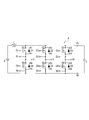
- the plane block diagram which arranged the six power module semiconductor devices which concern on embodiment, and comprised the 3-phase alternating current inverter.
- FIG. 17A is a schematic cross-sectional structure diagram taken along a line XVIIa-XVIIa in FIG. 16, and FIG. 16B is a schematic cross-sectional structure diagram taken along a line XVIIb-XVIIb in FIG. (A) Another schematic cross-sectional structure diagram along line XVIIa-XVIIa in FIG.
- FIG. 16 (b) Another schematic cross-sectional structure diagram along line XVIIb-XVIIb in FIG. (A) Another schematic cross-sectional structure diagram taken along line XVIIa-XVIIa in FIG. 16, (b) Still another schematic cross-sectional structure diagram along line XVIIb-XVIIb in FIG.
- FIG. 22 is a schematic cross-sectional structure diagram taken along line XXII-XXII in FIG. 21.
- the bird's-eye view which has arrange
- the circuit block diagram of the full bridge inverter comprised by arrange
- the plane block diagram which also includes the connection electrode (GNDL * POWL) between each power terminal which has arrange
- FIG. 4 is a schematic cross-sectional structure diagram of a SiC MOSFET that is an example of a semiconductor device applied to the power module semiconductor device according to the embodiment and includes a source pad electrode SP and a gate pad electrode GP.
- the circuit structural example which connected the snubber capacitor between the power terminal PL and the ground terminal NL in the schematic circuit structure of the three-phase alternating current inverter comprised using the power module semiconductor device which concerns on embodiment.
- FIG. 31 is a schematic cross-sectional structure diagram along XXXI-XXXI in FIG. 30B, in which a carbon jig on which a power module semiconductor device is mounted is mounted on a hot plate and cut in the longitudinal direction of the carbon jig.
- the typical cross-section figure explaining a transfer mold molding process.
- the typical cross-section figure explaining the process following FIG. 32 of transfer mold shaping
- the plane block diagram which also includes the connection wiring (bus-bar) electrode (GNDL * POWL) between each power terminal which has arrange
- the plane block diagram which also includes the connection electrode (GNDL * POWL) between each power terminal which has arrange
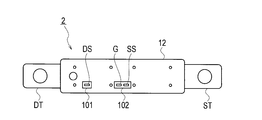
- a power module semiconductor device 2 having a straight wiring structure according to the present embodiment, and a bird's-eye view configuration of a 1 in 1 module is represented as shown in FIG.
- the signal system terminals SS ⁇ G ⁇ DS are arranged so as to protrude from the resin layer 12 in the vertical direction as shown in FIG. .
- 1 in 1 can be regarded as one large transistor, but there may be a plurality of built-in transistor devices. There are also 2 in 1, 4 in 1, 6 in 1, etc., but this is a module with two built-in transistors connected in the vertical direction on Fig. 28 (inverter circuit). Modules with built-in wiring are called 4 in 1, and those with all wiring are called 6 in 1.
- the signal system terminal DS is held in a state of being locked by a one-terminal holder 101 as a first locking member embedded in the main surface portion of the resin layer 12 at the same height as the mold surface.
- G ⁇ SS is held in a state of being locked by a two-terminal holder 102 as a first locking member embedded in the main surface portion of the resin layer 12 at the same height as the mold surface.
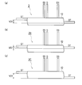
- FIG. 1 planar configuration of the power module semiconductor device 2 having a straight wiring structure according to the present embodiment is expressed as shown in FIG. 1 is represented as shown in FIG. 3 (a), and the side structure of another power module semiconductor device 2B in the direction of arrow III in FIG. 1 is shown in FIG. 3 (b).
- FIG. 3 (b) A side surface structure of yet another power module semiconductor device 2C in the direction of arrow III in FIG. 1 is represented as shown in FIG.
- FIG. IV in FIG. 1 is expressed as shown in FIG.
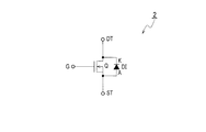
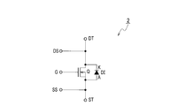
- the circuit representation of the one-in-one module is expressed as shown in FIG. Further, in the power module semiconductor device 2 according to the present embodiment, a detailed circuit representation of the one-in-one module is expressed as shown in FIG.
- the power module semiconductor device 2 has a one-in-one module configuration. That is, one MOSFET (semiconductor device) Q is built in one module. As an example, five chips (MOS transistors ⁇ 5) can be mounted as shown in FIG. 7, and up to five MOSFETs Q are connected in parallel. A part of the five chips can be mounted for the diode DI.
- MOSFET semiconductor device
- FIG. 5 shows a diode DI connected in reverse parallel between the source and drain of the MOSFET Q.
- the main electrode of the MOSFET Q is represented by a drain terminal DT and a source terminal ST as power system terminals.
- the diode DI is composed of a body Di or a body Di of an individual chip.
- SS is a source sense terminal
- DS is a drain sense terminal
- G is a gate signal terminal, both of which constitute a signal system terminal.
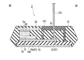
- FIG. 8 A schematic cross-sectional structure taken along line VIII-VIII in FIG. 7 is represented as shown in FIG. 8, and a schematic cross-sectional structure taken along line IX-IX in FIG. 7 is represented as shown in FIG.
- a schematic cross-sectional structure taken along line XX is represented as shown in FIG. 10, and a schematic cross-sectional structure taken along line XI-XI in FIG. 7 is represented as shown in FIG.
- the power module semiconductor device 2 having a straight wiring structure includes an insulating substrate 10 and a first pattern 10a (a copper plate layer 10a disposed on the insulating substrate 10). D), a semiconductor device Q arranged on the first pattern 10a (D), a power system terminal ST ⁇ DT and a signal system terminal DS ⁇ G ⁇ SS electrically connected to the semiconductor device Q, and a signal system 1 terminal holder 101 that locks the terminal DS, 2 terminal holder 102 that locks the signal system terminals G and SS, and the upper surface of the 1 terminal holder 101 and the 2 terminal holder 102 are exposed from the mold surface. And a resin layer 12 covering the device Q and the insulating substrate 10.
- the signal system terminals DS, G, and SS are arranged extending in a direction perpendicular to the main surface of the insulating substrate 10, and the power system terminals ST and DT are arranged in parallel with the main surface of the resin layer 12.
- the resin layers 12 are arranged extending in opposite directions from opposite side surfaces, and have a straight wiring structure.
- power system terminals ST and DT are arranged in parallel to the main surface from the side surface of resin layer 12 as shown in FIGS. ing.
- the power system terminals ST and DT are arranged along the longitudinal direction of the resin layer 12 so as to extend in opposite directions from the opposite side surfaces of the resin layer 12.
- the power system terminals ST / DT are arranged with predetermined steps VD1, VD2, and VD3 in the thickness direction of the resin layer 12, as shown in FIGS. 3 (a) to 3 (c).
- the direction perpendicular to the main surface of the insulating substrate 10 is equal to the direction perpendicular to the main surface of the resin layer 12.
- the signal system terminals DS, G, and SS may be arranged linearly on the main surface of the resin layer 12 as shown in FIGS.
- the signal system terminal may include a gate signal terminal G and a sensor terminal.
- the sensor terminal may include a source sense terminal SS and a drain sense terminal DS.
- the illustration is omitted, but the thermistor connection terminal for temperature sensing is perpendicular to the main surface of the insulating substrate 10 like the signal system terminal. You may arrange in.
- the power module semiconductor device 2 having a straight wiring structure includes an electrode pattern GSP / SSP arranged adjacent to the semiconductor device Q on the insulating substrate 10, as shown in FIG.
- the signal system terminals G ⁇ SS are connected to the electrode patterns GSP ⁇ SSP by soldering.
- the signal system terminal DS is connected to the first pattern 10a (D) by soldering.
- the drain sense terminal DS is connected to the first pattern 10 a (D) by soldering via the solder layer 3 c and is perpendicular to the main surface of the insulating substrate 10. It is arranged extending in the direction.
- the drain sense terminal DS is locked by the one-terminal holder 101, so that the solder layer 3c at the connection portion with the first pattern 10a (D) is protected. That is, the drain sense terminal DS is already soldered to the first pattern 10a (D) via the solder layer 3c before the molding process for forming the resin layer 12, and the state protruding in the vertical direction is 1 It is held by the terminal holder 101. Therefore, when the drain sense terminal DS is press-fitted into a metal tube such as a socket after resin molding, a load stress at the time of press-fitting is applied to the connection portion by the drain sense terminal DS or the solder layer 3c, or the drain sense terminal DS is caused by vibration during use. It is possible to prevent so-called terminal disconnection in which the sense terminal DS falls off from the metal tube.
- the gate signal terminal G is connected to the gate signal electrode pattern GSP by soldering via the solder layer 3c, and the gate signal electrode pattern GSP and the source sense electrode pattern SSP are connected. Between the first and second electrodes, bent upward and extending perpendicularly to the main surface of the insulating substrate 10. Further, the gate signal terminal G is locked by the two-terminal holder 102, so that the solder layer 3c at the connection portion with the gate signal electrode pattern GSP is protected.
- the source sense terminal SS is connected to the source sense electrode pattern SSP by soldering via the solder layer 3c, and the gate signal electrode pattern GSP and the source sense electrode pattern SSP are connected. Between the first and second electrodes, bent upward and extending perpendicularly to the main surface of the insulating substrate 10. Further, the source sense terminal SS is locked by the two-terminal holder 102, so that the solder layer 3c at the connection portion with the source sense electrode pattern SSP is protected.
- the gate signal terminal G and the source sense terminal SS are already solder-connected to the gate signal electrode pattern GSP and the source sense electrode pattern SSP through the solder layer 3c before the molding process for forming the resin layer 12.
- the state protruding in the vertical direction is held by the two-terminal holder 102. Therefore, by applying the gate signal terminal G and the source sense terminal SS to a metal tube such as a socket after resin molding, load stress at the time of press fitting is applied to the connection portion by the gate signal terminal G, the source sense terminal SS and the solder layer 3c. So that the gate signal terminal G and the source sense terminal SS fall out of the metal tube due to vibration during use or the like.
- gate signal terminal G and the source sense terminal SS may be individually locked by the one-terminal holder 101, similarly to the drain sense terminal DS.
- the insulating substrate 10 may be formed of a ceramic substrate.
- the ceramic substrate can be formed of, for example, Al 2 O 3 , AlN, SiN, AlSiC, or at least a surface of insulating SiC.
- the power module semiconductor device 2 is arranged on the second pattern 10a (S) of the first copper plate layer 10a and the semiconductor device Q as shown in FIGS.
- the columnar electrode 20, the upper surface plate electrode 22 disposed on the columnar electrode 20, the drain terminal DT disposed on the first pattern 10a (D), the second pattern 10a (S), and the upper A columnar connection electrode 18n connected to the face plate electrode 22 and a source terminal ST connected to the columnar connection electrode 18n are provided.
- the power system terminals ST and DT are connected to the source terminal ST connected to the source pad electrode SP (see FIG. 27) of the semiconductor device Q and to the drain electrode pattern D (see FIGS. 26 and 27) of the semiconductor device Q. And a drain terminal DT.
- the source terminal ST is connected to the source pad electrode SP of the semiconductor device Q, and the drain terminal DT is connected to the drain electrode pattern D of the semiconductor device Q.
- the gate signal terminal G and the source sense terminal SS of the semiconductor device Q are respectively connected to the gate signal electrode pattern GSP and the source sense electrode arranged adjacent to the semiconductor device Q through bonding wires. Bonded with the pattern SSP.
- first pattern 10a (D) and the semiconductor device Q are joined via the solder layer 3b
- second pattern 10a (S) and the columnar connection electrode 18n are also joined via the solder layer 3b.
- columnar electrode 20 and the upper surface plate electrode 22 are joined via the solder layer 3a, and the columnar connection electrode 18n, the upper surface plate electrode 22 and the source terminal ST are also joined via the solder layer 3a.
- the power module semiconductor device 2 may include a diode DI arranged adjacent to the semiconductor device Q on the first pattern 10a (D) in a one-in-one module configuration.
- the cathode K of the diode DI is connected to the first pattern 10 a (D), and the anode A is connected to the upper surface plate electrode 22 via the columnar electrode 20.
- the semiconductor device Q is formed of, for example, a SiC MOSFET, and the diode DI can be formed of, for example, a SiC Schottky barrier diode (SBD).
- SBD SiC Schottky barrier diode
- the second copper plate layer 10b disposed on the back surface of the insulating substrate 10 functions as a heat spreader.
- the resin layer 12 may be transfer molded with an epoxy resin or a silicone resin.
- the plurality of chips of the semiconductor device Q are arranged on the surface of the insulating substrate 10 at positions separated from each other in a plan view when viewed from the thickness direction of the insulating substrate 10 and are resin-molded by the resin layer 12.
- the columnar connection electrode 18n may be formed of an electrode material having a relatively small linear thermal expansion coefficient (CTE: Coefficient of Thermal Expansion), for example, CuMo, Cu, or the like.
- CTE Coefficient of Thermal Expansion
- the upper surface plate electrode 22 may be formed of an electrode material having a relatively small CTE value, for example, CuMo, Cu, or the like.
- the portion of the columnar electrode 20 may be formed of an electrode material having a relatively small CTE value, such as CuMo or Cu.
- the generated stress is larger in the material having a larger Young's modulus value. For this reason, a member with a small value of generated stress can be achieved by selecting a material having a smaller value of Young's modulus ⁇ CTE.
- CuMo has such advantages. Moreover, although CuMo is inferior to Cu, its electrical resistivity is relatively low.
- TLP Transient Liquid Phase
- the metal particle bonding is formed by baking a paste material containing conductive particles.
- the firing temperature of the paste material is, for example, about 200 to 400 ° C.
- the conductive particles are metal fine particles, such as silver particles, gold particles, nickel or copper particles.
- the concentration of silver particles is, for example, about 80% by mass to about 95% by mass.
- the average particle size is about 10 nm to about 100 nm.
- the metal terminal component is directly soldered to the electrode pattern or the like, so that a component such as a socket is not required.
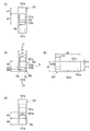
- the structure of the one-terminal holder 101 is shown in the four views shown in FIG. 12 (FIG. 12 (a) viewed from the top, and FIG. 12 (b) to FIG. 12 (d) viewed from each side). It is expressed as follows.
- the one-terminal holder 101 has a rectangular upper surface portion in the short direction of the power module semiconductor device 2.
- a drain sense terminal DS is inserted, and an opening 101b is provided for holding the inserted drain sense terminal DS in a locked state.
- a resin filling portion 101a connected to the opening 101b is formed inside the one-terminal holder 101. Further, as shown in FIG. 12C, an inlet 101c as a resin inlet hole connected to the resin filling portion 101a is opened on one side surface of the one-terminal holder 101. On the other hand, as shown in FIG. 12D, a delivery port 101d as a resin delivery hole connected to the resin filling portion 101a is opened on the other side surface of the one-terminal holder 101 facing the delivery port 101c.
- the inlet 101c is opened larger than the outlet 101d so that the resin filling portion 101a is sufficiently filled with the mold resin. That is, the one-terminal holder 101 has a resin filling portion made of mold resin by disposing the inlet 101c toward the upstream side of the mold resin injection and the outlet 101d toward the downstream side of the injection. It is possible to more reliably fill the interior of 101a. Thereby, sufficient insulation and strength within the one-terminal holder 101 are ensured.
- each part of the one-terminal holder 101 are expressed as follows (unit: mm).
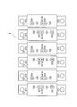
- the structure of the two-terminal holder 102 is as shown in a five-sided view in FIG. 13 (a view from the top in FIG. 13A and a view from each side in FIGS. 13B to 13E). expressed.
- the two-terminal holder 102 has a rectangular upper surface portion in the longitudinal direction of the power module semiconductor device 2.
- a gate signal terminal G is inserted into the upper surface portion of the two-terminal holder 102, an opening 102b for holding the inserted gate signal terminal G in a locked state, and a source sense terminal SS are inserted.
- an opening 102c that holds the inserted source sense terminal SS in a locked state.
- a resin filling portion 102a connected to the openings 102b and 102c is formed inside the two-terminal holder 102. Further, as shown in FIG. 13D, an inlet 102d as a resin inlet hole connected to the resin filling portion 102a is opened on one side surface of the two-terminal holder 102. On the other hand, on the other side surface of the two-terminal holder 102 facing the inlet port 102d, as shown in FIG. 13 (e), an outlet port 102e serving as a resin outlet hole connected to the resin filling portion 102a is opened.
- the inlet 102d is opened larger than the outlet 102e so that the resin filling portion 102a is sufficiently filled with the mold resin. That is, the two-terminal holder 102 has a resin filling portion made of mold resin by disposing the inlet 102d toward the upstream side of injection of the mold resin and the outlet 102e toward the downstream side of injection. It is possible to more reliably fill the inside of 102a. Thereby, sufficient insulation and strength in the two-terminal holder 102 are ensured.
- each part of the two-terminal holder 102 are expressed as follows (unit: mm ).
- the one-terminal holder 101 and the two-terminal holder 102 are plastic parts having predetermined heat resistance, such as high heat resistance such as PPS (polyphenylene sulfide) resin or PEEK (polyether ether ketone) resin, LCP (liquid crystal polymer) ( It is formed of a plastic (or engineering plastic or super engineering plastic) having 150 ° C. or higher, preferably 200 ° C. or higher.
- PPS polyphenylene sulfide
- PEEK polyether ether ketone
- LCP liquid crystal polymer
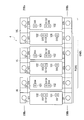
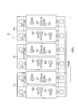
- FIG. 1 A schematic plan configuration in which six power module semiconductor devices 2 having a straight wiring structure according to the present embodiment are arranged to constitute a three-phase AC inverter device 4 is expressed as shown in FIG.
- the signal system terminals SS, G, and DS are not arranged on the outer periphery of the resin layer 12, they are arranged in parallel as shown in FIG. Also can reduce the distance between power modules.
- connection relationship between the terminals constituting the three-phase AC inverter device 4 by arranging six power module semiconductor devices 2 having a straight wiring structure according to the present embodiment is expressed as shown in FIG.
- connection wiring (bus bar) electrodes (GNDL ⁇ POWL) between the power terminals, in which six power module semiconductor devices 2 having a straight wiring structure according to the present embodiment are arranged to constitute a three-phase AC inverter device 4.
- the planar configuration is expressed as shown in FIG.
- Transistors Q1 and Q4, Q2 and Q5, and Q3 and Q6 each constitute a half-bridge inverter.
- the drain terminals DT1, DT2, and DT3 of the transistors Q1, Q2, and Q3 are commonly connected by a power supply bus bar electrode POWL, and the source terminals ST4 and ST5 of the transistors Q4, Q5, and Q6 are connected.
- ST6 is commonly connected by a grounding bus bar electrode GNDL.
- the source terminals ST1, ST2, and ST3 of the transistors Q1, Q2, and Q3 are connected to the drain terminals DT4, DT5, and DT6 of the transistors Q4, Q5, and Q6, respectively. Commonly connected by VL and WL. As a result, three-phase outputs of U, V, and W are obtained from the bus bar electrodes UL, VL, and WL.
- FIG. 17A a schematic cross-sectional structure taken along line XVIIa-XVIIa in FIG. 16 is represented as shown in FIG. 17A, and a schematic cross-sectional structure taken along line XVIIb-XVIIb in FIG. 16 is shown in FIG. Represented as shown.
- FIG. 18A another schematic cross-sectional structure taken along line XVIIa-XVIIa in FIG. 16 is represented as shown in FIG. 18A, and another schematic cross-sectional structure taken along line XVIIb-XVIIb in FIG. It is expressed as shown in (b).
- FIG. 19A Another schematic cross-sectional structure along the line XVIIa-XVIIa in FIG. 16 is expressed as shown in FIG. 19A, and yet another schematic cross-sectional structure along the line XVIIb-XVIIb in FIG. It is expressed as shown in FIG.
- the power system terminals ST ⁇ DT are arranged with predetermined steps VD1, VD2, and VD3 in the thickness direction of the resin layer 12, as shown in FIG.
- the example of 17 corresponds to the example having the predetermined step VD1 shown in FIG. 3A
- the example of FIG. 18 corresponds to the example having the predetermined step VD2 shown in FIG.
- the example of FIG. 19 corresponds to the example having the predetermined step VD3 shown in FIG.
- the bus bar electrodes UL, VL, and WL have a straight electrode structure as well as the bus bar electrodes POWL and GNDL as shown in FIG. Have.
- the bus bar electrodes POWL and GNDL have a straight electrode structure.
- the bus bar electrodes UL, VL, and WL are Since the value of the predetermined step VD2 is relatively small, the electrode structure is bent upward.
- the bus bar electrodes POWL and GNDL have a straight electrode structure.
- the bus bar electrodes UL, VL, and WL are Since the value of the predetermined step VD3 is relatively large, the electrode structure is bent downward.
- FIG. 1 In the three-phase AC inverter device 4 configured by arranging six power module semiconductor devices 2 having a straight wiring structure according to the present embodiment, an example in which the signal system terminals SS, G, and DS are arranged non-linearly is shown in FIG. As shown in FIG.
- the signal system terminals DS, G, and SS may be non-linearly arranged on the main surface of the resin layer 12.
- the signal system terminals DS, G, and SS may be randomly arranged on the main surface of the resin layer 12.
- Inverter device 4 in which a plurality of power module semiconductor devices 2 according to the present embodiment are arranged in parallel has a plurality of power module semiconductor devices 2 arranged in parallel as shown in FIGS.
- the power system terminals ST and DT of the device 2 are connected to each other via bus bar electrodes GNDL and POWL.
- the drain terminal DT and the source terminal ST of the power module semiconductor device 2 are the source terminals of the adjacent power module semiconductor devices 2.
- the ST and the drain terminal DT are arranged so as to face each other.
- a first transistor and a second transistor (Q1 and Q4) that form a half bridge. ), (Q2, Q5), (Q3, Q6) are arranged adjacent to each other, and the source terminal / drain terminal of the first transistor and the drain terminal / source terminal of the second transistor are arranged adjacent to each other. Yes.
- the source terminal / drain terminal (ST1, DT4) of the first transistor / second transistor (Q1, Q4), the drain terminal / source terminal (DT1, ST4) of the first transistor / second transistor (Q1, Q4), Source terminal / drain terminal (ST2, DT5) of the first transistor / second transistor (Q2, Q5), drain terminal / source terminal (DT2, ST5) of the first transistor / second transistor (Q2, Q5), first The source terminal / drain terminal (ST3 / DT6) of the transistor / second transistor (Q3 / Q6) and the drain terminal / source terminal (DT3 / ST6) of the first transistor / second transistor (Q3 / Q6) are adjacent to each other. Are arranged as follows.
- the power system terminals ST ⁇ DT of each set of the power module semiconductor devices 2 are connected to each other via the bus bar electrodes UL, VL, and WL, so that the three-phase The AC inverter device 4 can be configured compactly.
- the power module semiconductor device 2 Since the power module semiconductor device 2 according to the present embodiment has a stepped terminal structure in a straight wiring module structure, it is possible to realize wiring with a low inductance Ls of external wiring (busbar wiring).
- the drain terminal DT and the source terminal ST are arranged straight (straight) at both ends of the rectangular resin layer 12 in plan view, and the drain terminal DT.
- a three-phase AC inverter device (6 in 1) can be easily configured by arranging the modules side by side in parallel.
- the wiring length can be reduced as compared with the configuration in which the wiring (bus bar electrode) is bent to ensure the insulation distance.
- the parasitic inductance Ls can be reduced by about 10% compared to the conventional case.
- a three-phase AC inverter device 4 configured by arranging six power module semiconductor devices 2 according to the present embodiment is arranged on a plurality of power module semiconductor devices 2 arranged in parallel as shown in FIGS.
- a control board 6 for controlling the power module semiconductor device 2 and a plurality of power module semiconductor devices 2 arranged in parallel to supply power to the power module semiconductor device 2 and the control board 6 8 and the length in the vertical direction in which the signal system terminals DS, G, and SS extend is a length connectable to the control board 6 and the power supply board 8.
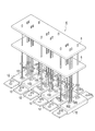
- FIG. 23 A bird's-eye view configuration diagram in which the control board 6 and the power supply board 8 are arranged on the three-phase AC inverter device 4 configured by arranging six power module semiconductor devices 2 according to the present embodiment is expressed as shown in FIG.
- the 23, the signal system terminals (DS1, G1, SS1), (DS2, G2, SS2), (DS3, G3, SS3), (DS4, G4, SS4), ( DS5, G5, SS5) and (DS6, G6, SS6) are connected in the vertical direction to the control board 6 and the power supply board 8, respectively, to constitute the three-phase AC inverter device 4.
- the detailed patterns of the control board 6 and the power supply board 8 are not shown for simplification.
- the distance between the power module semiconductor device 2 and the control board 6 / power supply board 8 in the vertical direction is relatively long.
- the top is arranged close to the distance.
- a control board 6 configured by arranging six power module semiconductor devices 2 having a straight wiring structure according to the present embodiment, a control board 6, a power supply board 8, a snubber capacitor C (not shown), and the like are arranged vertically. It becomes easy to arrange in a stacked structure, and the system can be slimmed.
- connection wiring (bus bar) electrodes (GNDL ⁇ POWL) between the power terminals in which the four power module semiconductor devices 2 according to the present embodiment are arranged to constitute the full bridge inverter device 5 is shown in FIG. As shown in FIG.
- a control board 6 (not shown), a power supply board 8 (not shown), and a snubber capacitor C (not shown).
- Etc. can be easily arranged in a vertically stacked structure, and the system can be slimmed.
- a schematic cross-sectional structure of an SiC MOSFET is an SiC semiconductor substrate composed of an n ⁇ high resistance layer as shown in FIG. 26, the p base region 28 formed on the surface side of the SiC semiconductor substrate 26, the source region 30 formed on the surface of the p base region 28, and the surface of the SiC semiconductor substrate 26 between the p base regions 28.
- an n + drain region 24 disposed on the n + drain region and a drain electrode 36 connected to the n + drain region 24.
- the semiconductor device 100 is composed of a planar gate type n-channel vertical SiC MOSFET, but may be composed of a trench gate type n-channel vertical SiC MOSFET or the like.
- an IGBT using a GaN-based FET or a SiC substrate can be applied instead of the SiC MOSFET.
- any of SiC-based, GaN-based, or AlN-based power devices can be applied.
- the semiconductor device 100 applied to the power module semiconductor device 2 according to the present embodiment has a band gap energy of, for example, a MOS transistor using a semiconductor substrate called a wide gap of 1.1 eV to 8 eV. Can be used.
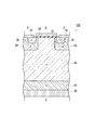
- FIG. 27 is an example of the semiconductor device 100 applied to the power module semiconductor device 2 according to the present embodiment, and a schematic cross-sectional structure of the SiC MOSFET including the source pad electrode SP and the gate pad electrode GP is as shown in FIG. Is done.
- the gate pad electrode GP is connected to the gate electrode 38 disposed on the gate insulating film 32, and the source pad electrode SP is connected to the source electrode 34 connected to the source region 30 and the p base region 28.
- the gate pad electrode GP and the source pad electrode SP are disposed on a passivation interlayer insulating film 44 covering the surface of the semiconductor device 100.
- the source pad electrode SP may be extended and disposed on the interlayer insulating film 44 for passivation.
- a circuit configuration in which the snubber capacitor C is connected between the power supply terminal PL and the ground terminal NL is expressed as shown in FIG.
- a large surge voltage Ldi / dt is generated due to the high switching speed of the SiC device due to the inductance L of the connection line.
- the surge voltage Ldi / dt varies depending on the value of the inductance L
- the surge voltage Ldi / dt is superimposed on the storage battery E.
- the surge voltage Ldi / dt can be absorbed by the snubber capacitor C connected between the power supply terminal PL and the ground terminal NL.
- the three-phase AC inverter includes a gate drive unit 50, a power module unit 52 connected to the gate drive unit 50, and a three-phase AC motor unit 54.
- the power module unit 52 is connected to U-phase, V-phase, and W-phase inverters corresponding to the U-phase, V-phase, and W-phase of the three-phase AC motor unit 54.
- the gate drive unit 50 is connected to the SiC MOSFETs Q1 and Q4 in FIG. Although not shown, it is also connected to SiC MOSFETs Q2 and Q5 and SiC MOSFETs Q3 and Q6.
- the power module unit 52 includes inverter-structured SiC MOSFETs Q1 and Q4, Q2 and Q5 between a plus terminal (+) and a minus terminal ( ⁇ ) to which a converter 48 connected to a storage battery (E) 46 is connected. And Q3 and Q6 are connected. Furthermore, diodes D1 to D6 are connected in antiparallel between the sources and drains of the SiC MOSFETs Q1 to Q6, respectively.
- a three-phase power module part 52 can also be formed.
- the carbon jig 400 includes a substrate insertion portion 402 at the center and recessed drain terminal DT placement portions 401a and source terminal ST placement portions 401b at both left and right ends.
- FIG. 1 a schematic cross section in which the power module semiconductor device 2 is mounted on the carbon jig 400, the carbon jig 400 on which the power module semiconductor device 2 is mounted is mounted on the hot plate 403, and is cut in the longitudinal direction of the carbon jig 400.
- the structure is represented as shown in FIG.
- FIG. 31 corresponds to the schematic cross-sectional structure along XXXI-XXXI in FIG. 30B, and the soldering process of the power system terminals ST / DT and the signal system terminals DS / G / SS is performed. Is shown. However, the signal system terminals DS, G, and SS indicate the relative positions of the signal systems terminals DS, G, and SS by broken lines.
- the signal system terminal DS can be soldered to the first pattern 10a (D), and the signal system terminal G ⁇ SS can be soldered to the electrode pattern GSP ⁇ SSP.
- the power system terminals ST ⁇ DT can be soldered to the columnar connection electrodes 18 n and the first pattern 10 a (D) of the power module semiconductor device 2.
- the hot plate 403 is heated to about 340 ° C. to 360 ° C., for example.
- the 1-terminal holder 101 is engaged with the soldered signal system terminal DS, and the 2-terminal holder 102 is engaged with the soldered signal system terminal G / SS. After that, a sealing step is performed.
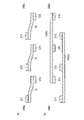
- FIGS. 1-10 a schematic cross-sectional structure for explaining the transfer mold forming step is expressed as shown in FIGS.
- FIGS. 32 to 34 the structure in which the one-terminal holder 101 and the two-terminal holder 102 are attached to the signal system terminals DS, G, and SS through the manufacturing process is turned upside down.
- a state is shown in which the upper mold 220 and the lower mold 200 are removed after the resin layer 12 is formed by being sandwiched between the mold 200) and the lower mold (first mold) 200 and encapsulating the mold resin.
- 202 and 203 are main body placing portions and terminal placing portions
- 204a and 204b are housing portions for signal system terminals DS, G, and SS
- 223 is a resin injecting portion.
- the 1-terminal holder 101 and the 2-terminal holder 102 attached so as to be taller than the mold surface by the height da ( ⁇ )
- the upper and lower parts of the body are sandwiched between the upper mold 220 and the lower mold 200, they are pressed in the vertical direction by the lower mold 200.
- the resin injection into the resin injection portion 223 is executed.
- the signal system terminals DS, G, and SS are supported by the one terminal holder 101 and the two terminal holder 102 in a state of protruding in the vertical direction. There is no need to add a process for bending and securing insulation of the system terminals DS, G, and SS, thereby reducing the number of processes and the risk of failure.
- a load stress applied when the signal system terminals DS, G, and SS are press-fitted into the socket is applied to the power module semiconductor device 2, and the signal system terminals DS, G, and SS are caused by vibration during long-term use. It is possible to prevent the device 2 from coming off.
- power system terminals ST and DT are further extended in the direction perpendicular to the main surface of insulating substrate 10. It is set as the composition.
- the power system terminal DT arranged in the vertical direction is arranged in the power system arranged in the vertical direction by the one-terminal holder (second locking member) 103.
- the terminals ST are held by the one-terminal holder (second locking member) 104 so as to be locked.
- the one-terminal holders 103 and 104 those having the same configuration as the one-terminal holder 101 can be used except for the dimensions.
- the power module semiconductor device 2A According to the configuration of the power module semiconductor device 2A according to the other embodiment of the present invention, not only the signal system terminals DS, G, and SS but also the power system terminals ST and DT can be prevented from being damaged due to load stress at the time of press-fitting. This prevents terminal disconnection due to vibration during use.
- FIG. 36 shows a planar configuration in which six power module semiconductor devices 2A according to another embodiment of the present invention are arranged in parallel to constitute a three-phase AC inverter device 4A.
- FIG. 37 shows a planar configuration in which four power module semiconductor devices 2A according to another embodiment of the present invention are arranged in parallel to form a full bridge inverter device 5A.
- the power system terminals ST and DT protrude in the vertical direction by the one terminal holders 103 and 104. Since it is supported, the size can be further reduced, and the three-phase AC inverter device 4A and the full-bridge inverter device 5A can be configured more compactly.
- the signal system terminals SS / G / DS and the power system terminals ST / DT are not arranged on the outer periphery of the resin layer 12, so that FIG. As shown in 37, the distance between the power modules can be further reduced even if they are arranged in parallel.
- the terminals DS, G, SS, ST, and DT can be pulled out in the vertical direction, the wiring in the module can be shortened, which contributes to noise resistance and loss reduction. Applications are expected.
- a power module semiconductor device that can be miniaturized and that can improve breakage due to load stress and terminal disconnection, a manufacturing method thereof, and an inverter device having the power module semiconductor device.
- the power module semiconductor device can be used for all power devices such as SiC power semiconductor modules, and particularly, in fields where miniaturization and weight reduction are required, in-vehicle / solar cells / industrial equipment / consumer equipment. It can be applied to a wide range of application fields such as inverters and converters.
- Gate drive unit 52 ... Power module unit 54 ... Three-phase AC motor unit 100, Q, Q1 to Q6 ... Semiconductor device (SiC MOSFET, semiconductor chip) 101 ... 1 terminal holder (first locking member) 101a ... Resin filling part 101b ... Opening part 101c ... Inlet (inlet hole) 101d ... Outlet (outlet) 102 ... Two-terminal holder (first locking member) 102a ... Resin filling portion 102b, 102c ... Opening portion 102d ... Inlet (inlet hole) 102e ... Sending port (sending hole) 103, 104 ... 1 terminal holder (second locking member) 200 ... Lower molds 204a and 204b ... Housing part 220 ...
Landscapes
- Engineering & Computer Science (AREA)
- Power Engineering (AREA)
- Inverter Devices (AREA)
- Structures Or Materials For Encapsulating Or Coating Semiconductor Devices Or Solid State Devices (AREA)
Abstract
パワーモジュール半導体装置(2)は、絶縁基板(10)と、絶縁基板(10)上に配置された銅プレート層(10a)の第1パターン(10a(D))と、第1パターン(10a(D))上に配置された半導体デバイスQと、半導体デバイスQと電気的に接続される電力系端子ST・DTおよび信号系端子DS・G・SSと、信号系端子DSを係止する1端子ホルダ(101)と、信号系端子G・SSを係止する2端子ホルダ(102)と、1端子ホルダ(101)および2端子ホルダ(102)の上面部をモールド面に露出させるようにして半導体デバイスQおよび絶縁基板(10)を被覆する樹脂層(12)とを備える。小型化が可能であり、荷重応力による破損や端子抜けを改善できるパワーモジュール半導体装置およびその製造方法、およびこのパワーモジュール半導体装置を有するインバータ装置を提供する。
Description
本実施の形態は、パワーモジュール半導体装置およびその製造方法、およびインバータ装置に関する。
現在多くの研究機関において、シリコンカーバイド(SiC:Silicon Carbide)デバイスの研究開発が行われている。SiCパワーデバイスの特長として、従来のSiパワーデバイスよりも低オン抵抗であり、高速スイッチングおよび高温動作などを挙げることができる。
絶縁ゲートバイポーラトランジスタ(IGBT:Insulated Gate Bipolar Transistor)などの従来のSiパワーデバイスでは、動作可能な温度範囲が150℃程度までである。
しかしながら、SiCパワーデバイスでは、理論的には、約600℃まで動作可能である。
従来のSiパワーモジュールでは、Siパワーデバイスのオン抵抗を下げるためにデバイス面積を大きくする必要があり、パワーモジュールの小型化に限界があった。
SiCパワーモジュールでは、SiCデバイスのオン抵抗が低いために面積の小さいデバイスでも大電流を導通することができ、SiCパワーモジュールの小型化が可能となる。
これらのSiCパワーデバイスのパッケージには、ケース型が採用されていたり、特許文献1のようにトランスファモールド成形された半導体装置や、特許文献2のようにソケットを一体成型し、端子を圧入してプレスフィット垂直端子を形成するトランスファモールドについて開示されているものもある。
しかしながら、特許文献1に記載のように、トランスファモールド成形された半導体装置は、端子列がパッケージ部の外周面に対して水平方向に配置されるのが一般的であったため、小型化に不向きであるという問題があった。
これに対し、特許文献2に記載の電力用半導体モジュールは、端子をモールド樹脂の表面に対して垂直方向に配置することによって、トランスファモールドモジュールの小型化を可能にしたものである。
ところが、この電力用半導体モジュールは、樹脂モールド後に金属筒に外部端子を圧入させることによって、モールド樹脂の表面より垂直方向に外部端子を配置するようにしたものであるため、圧入時に荷重応力が加えられることや、使用中の振動などにより外部端子が金属筒から抜け落ちる端子抜けといった問題が懸念されていた。
本実施の形態は、小型化が可能であり、荷重応力による破損や端子抜けを改善できるパワーモジュール半導体装置およびその製造方法、およびこのパワーモジュール半導体装置を有するインバータ装置を提供する。
本実施の形態の一態様によれば、絶縁基板と、前記絶縁基板上に配置された銅プレート層の第1パターンと、前記第1パターン上に配置された半導体デバイスと、前記半導体デバイスと電気的に接続された電力系端子と、前記半導体デバイスと電気的に接続されると共に、前記絶縁基板の主表面に対して垂直方向に延伸して配置された信号系端子と、前記信号系端子を係止する第1の係止部材と、前記第1の係止部材の一部を露出させるようにして、前記半導体デバイスおよび前記絶縁基板を被覆する樹脂層とを備えるパワーモジュール半導体装置が提供される。
また、本実施の形態の他の態様によれば、上記のパワーモジュール半導体装置を複数有し、前記樹脂層は長手方向と短手方向とを有する平面視矩形状をしており、各パワーモジュール半導体装置をその短手方向に近接して配置したインバータ装置が提供される。
また、本実施の形態の他の態様によれば、絶縁基板上に配置された銅プレート層の第1パターン上に配置された半導体デバイスと、前記半導体デバイスと電気的に接続された電力系端子と、前記半導体デバイスと電気的に接続されると共に、前記絶縁基板の主表面に対して垂直方向に延伸して配置された信号系端子と、前記信号系端子を係止する第1の係止部材と、を含んで、前記絶縁基板の垂直方向に対向する両表面側を第1の金型および第2の金型により保持する第1の工程と、前記第1の金型および前記第2の金型内に樹脂を充填させ、前記第1の係止部材の一部を露出させるようにして、前記半導体デバイスおよび前記絶縁基板を被覆する樹脂層を形成する第2の工程とを有するパワーモジュール半導体装置の製造方法が提供される。
本実施の形態によれば、小型化が可能であり、荷重応力による破損や端子抜けを改善できるパワーモジュール半導体装置およびその製造方法、およびこのパワーモジュール半導体装置を有するインバータ装置を提供することができる。
次に、図面を参照して、実施の形態を説明する。以下の図面の記載において、同一または類似の部分には同一または類似の符号を付している。ただし、断面図は模式的なものであり、厚みと平面寸法との関係、各層の厚みの比率などは現実のものとは異なることに留意すべきである。したがって、具体的な厚みや寸法は以下の説明を参酌して判断すべきものである。また、図面相互間においても互いの寸法の関係や比率が異なる部分が含まれていることはもちろんである。
また、以下に示す実施の形態は、技術的思想を具体化するための装置や方法を例示するものであって、この実施の形態は、構成部品の材質、形状、構造、配置などを下記のものに特定するものでない。この実施の形態は、特許請求の範囲において、種々の変更を加えることができる。
[パワーモジュール半導体装置の構成]
本実施の形態に係るストレート配線構造のパワーモジュール半導体装置2であって、ワンインワンモジュール(1 in 1 Module)の鳥瞰構成は、図1に示すように表される。本実施の形態に係るストレート配線構造のパワーモジュール半導体装置2においては、信号系端子SS・G・DSは、図1に示すように、樹脂層12から垂直方向に突き出したように配置されている。
本実施の形態に係るストレート配線構造のパワーモジュール半導体装置2であって、ワンインワンモジュール(1 in 1 Module)の鳥瞰構成は、図1に示すように表される。本実施の形態に係るストレート配線構造のパワーモジュール半導体装置2においては、信号系端子SS・G・DSは、図1に示すように、樹脂層12から垂直方向に突き出したように配置されている。
1 in 1は、一つの大きなトランジスタとみることができるが、内蔵されているトランジスタデバイスは、複数個である場合もある。2 in 1、4 in 1、6 in 1などもあるが、これは、図28(インバータ装置回路)上において、縦2個分のトランジスタを接続内蔵したモジュールを2 in 1、2 in 1を2組配線内蔵したモジュールを4 in 1、全て配線内蔵したものが6 in 1と呼ばれている。
信号系端子DSは、樹脂層12の主表面部にモールド面と同一の高さで埋設された第1の係止部材としての1端子ホルダ101によって係止された状態で保持され、信号系端子G・SSは、樹脂層12の主表面部にモールド面と同一の高さで埋設された第1の係止部材としての2端子ホルダ102によって係止された状態で保持されている。
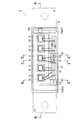
また、本実施の形態に係るストレート配線構造のパワーモジュール半導体装置2の平面構成は、図2に示すように表される。また、図1の矢印III方向の側面構造は、図3(a)に示すように表され、図1の矢印III方向の別のパワーモジュール半導体装置2Bの側面構造は、図3(b)に示すように表され、図1の矢印III方向のさらに別のパワーモジュール半導体装置2Cの側面構造は、図3(c)に示すように表される。また、図1の矢印IV方向の側面構造は、図4に示すように表される。
本実施の形態に係るパワーモジュール半導体装置2であって、ワンインワンモジュールの回路表現は、図5に示すように表される。また、本実施の形態に係るパワーモジュール半導体装置2であって、ワンインワンモジュールの詳細回路表現は、図6に示すように表される。
本実施の形態に係るパワーモジュール半導体装置2は、ワンインワンモジュールの構成を備える。すなわち、1個のMOSFET(半導体デバイス)Qが1つのモジュールに内蔵されている。一例として、図7に示すように5チップ(MOSトランジスタ×5)搭載可能であり、それぞれのMOSFETQは、5個までが並列接続される。なお、5チップの内、一部をダイオードDI用として搭載することも可能である。
図5には、MOSFET Qのソース・ドレイン間に逆並列接続されるダイオードDIが示されている。MOSFET Qの主電極は、電力系端子としてのドレイン端子DTおよびソース端子STで表される。ダイオードDIは、ボディDiまたは個別チップのボディDiから構成される。
なお、図6において、SSは、ソースセンス端子、DSは、ドレインセンス端子であり、Gは、ゲート信号端子であり、いずれも信号系端子を構成している。
本実施の形態に係るストレート配線構造のパワーモジュール半導体装置2の平面パターン構成は、図7に示すように表される。図7のVIII-VIII線に沿う模式的断面構造は、図8に示すように表され、図7のIX-IX線に沿う模式的断面構造は、図9に示すように表され、図7のX-X線に沿う模式的断面構造は、図10に示すように表され、図7のXI-XI線に沿う模式的断面構造は、図11に示すように表される。
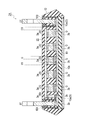
本実施の形態に係るストレート配線構造のパワーモジュール半導体装置2は、図7および図8に示すように、絶縁基板10と、絶縁基板10上に配置された銅プレート層10aの第1パターン10a(D)と、第1パターン10a(D)上に配置された半導体デバイスQと、半導体デバイスQと電気的に接続される電力系端子ST・DTおよび信号系端子DS・G・SSと、信号系端子DSを係止する1端子ホルダ101と、信号系端子G・SSを係止する2端子ホルダ102と、1端子ホルダ101および2端子ホルダ102の上面部をモールド面から露出させるようにして半導体デバイスQおよび絶縁基板10を被覆する樹脂層12とを備える。
ここで、信号系端子DS・G・SSは、絶縁基板10の主表面に対して垂直方向に延伸して配置され、電力系端子ST・DTは、樹脂層12の主表面と平行に、樹脂層12の長手方向に沿って、樹脂層12の対向する両側面から互いに逆方向に延伸して配置され、ストレート配線構造を有する。
本実施の形態に係るストレート配線構造のパワーモジュール半導体装置2においては、電力系端子ST・DTは、図7および図8に示すように、樹脂層12の側面から主表面と平行方向に配置されている。
また、電力系端子ST・DTは、樹脂層12の長手方向に沿って、樹脂層12の対向する両側面から互いに逆方向に延伸して配置される。
なお、電力系端子ST・DTは、図3(a)~図3(c)に示すように、樹脂層12の厚み方向に、所定の段差VD1・VD2・VD3をもって配置される。
また、絶縁基板10の主表面に対する垂直方向は、樹脂層12の主表面に対する垂直方向に等しい。
一方、信号系端子DS・G・SSは、図1および図2に示すように、樹脂層12の主表面上に直線状に配置されていても良い。
また、信号系端子は、ゲート信号端子Gおよびセンサ用端子を備えていても良い。また、センサ用端子は、ソースセンス端子SSおよびドレインセンス端子DSを備えていても良い。
ここで、ソースセンス端子SS、ドレインセンス端子DSの他に、図示は省略されているが、温度センス用にサーミスタ接続端子などを信号系端子と同様に絶縁基板10の主表面に対して垂直方向に配置しても良い。
また、本実施の形態に係るストレート配線構造のパワーモジュール半導体装置2は、図7に示すように、絶縁基板10上に、半導体デバイスQに隣接して配置された電極パターンGSP・SSPを備え、信号系端子G・SSは、電極パターンGSP・SSPに半田付けにより接続されている。信号系端子DSは、第1パターン10a(D)に半田付けにより接続されている。
ドレインセンス端子DSは、図7および図9に示すように、第1パターン10a(D)に対して半田層3cを介して半田付けにより接続されており、絶縁基板10の主表面に対して垂直方向に延伸して配置される。
また、ドレインセンス端子DSは、1端子ホルダ101によって係止されることにより、第1パターン10a(D)との接続部の半田層3cが保護されている。すなわち、ドレインセンス端子DSは、樹脂層12を形成するモールド工程前の段階ですでに半田層3cを介して第1パターン10a(D)に半田接続されると共に、垂直方向に突き出した状態が1端子ホルダ101によって保持される。したがって、樹脂モールド後にソケットなどの金属筒にドレインセンス端子DSを圧入させることにより、ドレインセンス端子DSや半田層3cによる接続部に圧入時の荷重応力が加えられたり、使用中の振動などによりドレインセンス端子DSが金属筒から抜け落ちたりする、いわゆる端子抜けを防止できる。
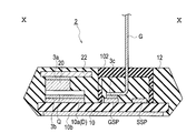
ゲート信号端子Gは、図7および図10に示すように、ゲート信号電極パターンGSPに対して半田層3cを介して半田付けにより接続されており、かつゲート信号電極パターンGSPとソースセンス電極パターンSSPとの相互間において上方に曲げられて絶縁基板10の主表面に対して垂直方向に延伸して配置される。また、ゲート信号端子Gは、2端子ホルダ102によって係止されることにより、ゲート信号電極パターンGSPとの接続部の半田層3cが保護されている。
ソースセンス端子SSは、図7および図11に示すように、ソースセンス電極パターンSSPに対して半田層3cを介して半田付けにより接続されており、かつゲート信号電極パターンGSPとソースセンス電極パターンSSPとの相互間において上方に曲げられて絶縁基板10の主表面に対して垂直方向に延伸して配置される。また、ソースセンス端子SSは、2端子ホルダ102によって係止されることにより、ソースセンス電極パターンSSPとの接続部の半田層3cが保護されている。
すなわち、ゲート信号端子Gおよびソースセンス端子SSは、樹脂層12を形成するモールド工程前の段階ですでに半田層3cを介してゲート信号電極パターンGSPおよびソースセンス電極パターンSSPに半田接続されると共に、垂直方向に突き出した状態が2端子ホルダ102によって保持される。したがって、樹脂モールド後にソケットなどの金属筒にゲート信号端子Gおよびソースセンス端子SSを圧入させることにより、ゲート信号端子Gおよびソースセンス端子SSや半田層3cによる接続部に圧入時の荷重応力が加えられたり、使用中の振動などによりゲート信号端子Gおよびソースセンス端子SSが金属筒から抜け落ちたりする、いわゆる端子抜けを防止できる。
なお、ゲート信号端子Gおよびソースセンス端子SSは、ドレインセンス端子DSと同様に、1端子ホルダ101によって個々に係止されるようにしても良い。
一方、絶縁基板10は、セラミック基板で構成されていても良い。ここで、セラミック基板は、例えば、Al2 O3 、Al N、SiN、AlSiC、もしくは、少なくとも表面が絶縁性のSiCで形成可能である。
さらに、本実施の形態に係るパワーモジュール半導体装置2は、図7および図8に示すように、第1の銅プレート層10aの第2パターン10a(S)と、半導体デバイスQ上に配置された柱状電極20と、柱状電極20上に配置された上面板電極22と、第1パターン10a(D)上に配置されたドレイン端子DTと、第2パターン10a(S)上に配置され、かつ上面板電極22と接続された柱状接続電極18nと、柱状接続電極18nに接続されたソース端子STとを備える。
電力系端子ST・DTは、半導体デバイスQのソースパッド電極SP(図27参照)に接続されたソース端子STと、半導体デバイスQのドレイン電極パターンD(図26および図27参照)に接続されたドレイン端子DTとを備える。また、ソース端子STは、半導体デバイスQのソースパッド電極SPに接続され、ドレイン端子DTは、半導体デバイスQのドレイン電極パターンDに接続される。
また、半導体デバイスQのゲート信号端子Gおよびソースセンス端子SSは、図7に示すように、ボンディングワイヤを介して、それぞれ半導体デバイスQに隣接して配置されたゲート信号電極パターンGSPおよびソースセンス電極パターンSSPとボンディング接続される。
また、第1パターン10a(D)と半導体デバイスQは、半田層3bを介して接合され、第2パターン10a(S)と柱状接続電極18nも半田層3bを介して接合される。
また、柱状電極20と上面板電極22は、半田層3aを介して接合され、柱状接続電極18nと上面板電極22およびソース端子STも半田層3aを介して接合される。
本実施の形態に係るパワーモジュール半導体装置2は、ワンインワン型モジュール構成において、第1パターン10a(D)上に半導体デバイスQに隣接して配置されたダイオードDIを備えていても良い。このダイオードDIのカソードKは、第1パターン10a(D)に接続され、アノードAは、柱状電極20を介して上面板電極22に接続される。
ここで、半導体デバイスQは、例えば、SiC MOSFETで形成され、ダイオードDIは、例えば、SiCショットキーバリアダイオード(SBD:Schottky Barrier Diode)で形成可能である。
絶縁基板10の裏面上に配置される第2の銅プレート層10bは、ヒートスプレッダとして機能する。
また、樹脂層12は、エポキシ系樹脂もしくはシリコーン系樹脂などでトランスファモールド成形されていても良い。
半導体デバイスQの複数のチップは、絶縁基板10の表面上に、絶縁基板10の厚み方向から見た平面視で離間した位置に配置され、樹脂層12により樹脂モールドされている。
また、柱状接続電極18nは、線熱膨張係数(CTE:Coefficient of Thermal Expansion)の値が相対的に小さい電極材料、例えば、CuMo、Cuなどで形成されていても良い。
上面板電極22の部分は、CTEの値が相対的に小さい電極材料、例えば、CuMo、Cuなどで形成されていても良い。
柱状電極20の部分は、CTEの値が相対的に小さい電極材料、例えば、CuMo、Cuなどで形成されていても良い。
CTEの値が同等である同じ大きさの材料を比較すると、発生応力は、ヤング率の値が大きい材料の方が大きくなる。このため、ヤング率×CTEの数値が、より小さい材料を選定することによって、発生応力の値の小さな部材を達成することができる。
CuMoは、このような利点を有している。また、CuMoは、Cuには劣るが、電気抵抗率も相対的に低い。
各部材の接合構造の形成には、半田接合の他に、金属粒子接合、固相拡散接合、液相拡散(TLP:Transient Liquid Phase)接合などの技術を適用可能である。
例えば、金属粒子接合は、導電性粒子を含むペースト材料を焼成して形成される。ペースト材料の焼成温度は、例えば、約200~400℃である。導電性粒子は、金属微粒子であり、例えば、銀粒子、金粒子またはニッケルや銅粒子などである。例えば、金属微粒子として銀粒子を適用する場合、銀粒子の濃度は、例えば、約80質量%~約95質量%である。また、銀ナノ粒子の場合の平均粒径は、約10nm~約100nm程度である。
本実施の形態に係るパワーモジュール半導体装置2の垂直端子内部構造においては、金属端子部品を電極パターンなどに対して直に半田付けなどを行うため、ソケットなどの部品を必要としない。
ここで、1端子ホルダ101の構造は、図12に示す四面図(図12(a)に上面から見た図、図12(b)~図12(d)に各側面から見た図)のように表される。1端子ホルダ101は、図12(a)に示すように、パワーモジュール半導体装置2の短手方向に長方形状の上面部を有している。1端子ホルダ101の上面部には、ドレインセンス端子DSが挿入されると共に、その挿入されたドレインセンス端子DSを係止した状態で保持する開口部101bが設けられている。
1端子ホルダ101の内部には、図12(b)に示すように、開口部101bにつながる樹脂充填部101aが形成されている。また、1端子ホルダ101の一方の側面には、図12(c)に示すように、樹脂充填部101aにつながる樹脂送入穴としての送入口101cが開口されている。一方、送入口101cに対向する、1端子ホルダ101の他方の側面には、図12(d)に示すように、樹脂充填部101aにつながる樹脂送出穴としての送出口101dが開口されている。
本実施の形態において、1端子ホルダ101は、樹脂充填部101a内がモールド樹脂により十分に充填されるようにするために、送入口101cが送出口101dよりも大きく開口されている。すなわち、1端子ホルダ101は、モールド樹脂の注入の上流側に向かって送入口101cを、注入の下流側に向かって送出口101dを、それぞれ対応させて配置することにより、モールド樹脂によって樹脂充填部101a内をより確実に充填させることが可能である。これにより、1端子ホルダ101内における絶縁性および強度が十分に確保される。
なお、一例として、ドレインセンス端子DSの断面寸法を1.5mm×0.5mmとした場合の、1端子ホルダ101の各部の寸法は以下のように表される(単位はmm)。例えば、図12(a)~図12(d)において、d1=2.7、d2=3.35、d3=8.2+α、d11=2.1、d12=2.75、d13=1.5、d14=0.3、d21=1.8、d22=0.7、d23=2.0、d31=3.5、d32=2.1、d33=2.0、d41=2.1、d42=2.0、d43=2.0。
また、Ra部~Re部の曲率は、Rを曲率半径とすると、Ra=2-R0.35、Rb=Rc=Rd=Re=4-R0.5。
ただし、モールド工程前の製造工程において、1端子ホルダ101は、樹脂層12のモールド面(垂直方向の主表面)よりもαの分だけ背高になるよう、d3が設計されている(例えば、α=10μm~200μm程度)。
2端子ホルダ102の構造は、図13に示す五面図(図13(a)に上面から見た図、図13(b)~図13(e)に各側面から見た図)のように表される。2端子ホルダ102は、図13(a)に示すように、パワーモジュール半導体装置2の長手方向に長方形状の上面部を有している。2端子ホルダ102の上面部には、ゲート信号端子Gが挿入されると共に、その挿入されたゲート信号端子Gを係止した状態で保持する開口部102bと、ソースセンス端子SSが挿入されると共に、その挿入されたソースセンス端子SSを係止した状態で保持する開口部102cと、が設けられている。
2端子ホルダ102の内部には、図13(b)および図13(c)に示すように、開口部102b・102cにつながる樹脂充填部102aが形成されている。また、2端子ホルダ102の一方の側面には、図13(d)に示すように、樹脂充填部102aにつながる樹脂送入穴としての送入口102dが開口されている。一方、送入口102dに対向する、2端子ホルダ102の他方の側面には、図13(e)に示すように、樹脂充填部102aにつながる樹脂送出穴としての送出口102eが開口されている。
本実施の形態において、2端子ホルダ102は、樹脂充填部102a内がモールド樹脂により十分に充填されるようにするために、送入口102dが送出口102eよりも大きく開口されている。すなわち、2端子ホルダ102は、モールド樹脂の注入の上流側に向かって送入口102dを、注入の下流側に向かって送出口102eを、それぞれ対応させて配置することにより、モールド樹脂によって樹脂充填部102a内をより確実に充填させることが可能である。これにより、2端子ホルダ102内における絶縁性および強度が十分に確保される。
なお、一例として、ゲート信号端子Gおよびソースセンス端子SSの断面寸法を1.5mm×0.5mmとした場合の、2端子ホルダ102の各部の寸法は以下のように表される(単位はmm)。例えば、図13(a)~図13(e)において、e1=8.4、e2=4.0、e3=8.6+α、e11=7.8、e13=6.7、e21=1.8、e22=0.7、e23=5.08、e31=3.5、e32=5.0、e33=2.0、e41=3.0、e42=2.0、e43=2.0、e51=0.4、e52=0.5、e53=1.0。
また、Pa部~Pe部の曲率は、Rを曲率半径とすると、Pa=4-R0.35、Pb=Pc=Pd=Pe=4-R0.5。
ただし、モールド工程前の製造工程において、2端子ホルダ102は、樹脂層12のモールド面よりもαの分だけ背高になるよう、e3が設計されている(例えば、α=10μm~200μm程度)。
また、1端子ホルダ101および2端子ホルダ102は所定の耐熱性を有するプラスチック部品、例えば、PPS(ポリフェニレンサルファイド)樹脂またはPEEK(ポリエーテルエーテルケトン)樹脂、LCP(液晶ポリマー)などの高耐熱性(150℃以上、好ましくは200℃以上)を有するプラスチック(または、エンジニアリングプラスチック、スーパーエンジニアリングプラスチック)により形成される。
[3相交流インバータの構成]
本実施の形態に係るストレート配線構造のパワーモジュール半導体装置2を6個配置して3相交流インバータ装置4を構成した模式的平面構成は、図14に示すように表される。
本実施の形態に係るストレート配線構造のパワーモジュール半導体装置2を6個配置して3相交流インバータ装置4を構成した模式的平面構成は、図14に示すように表される。
本実施の形態に係るストレート配線構造のパワーモジュール半導体装置2においては、樹脂層12の外周に信号系端子SS・G・DSを配置していないので、図14に示すように、並列配置してもパワーモジュール間距離を詰めることができる。
また、本実施の形態に係るストレート配線構造のパワーモジュール半導体装置2を6個配置して3相交流インバータ装置4を構成した各端子間の接続関係は、図15に示すように表される。
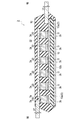
また、本実施の形態に係るストレート配線構造のパワーモジュール半導体装置2を6個配置して3相交流インバータ装置4を構成した各パワー端子間の接続配線(バスバー)電極(GNDL・POWL)も含む平面構成は、図16に示すように表される。
トランジスタQ1・Q4、Q2・Q5、Q3・Q6は、それぞれハーフブリッジのインバータを構成する。
図15および図16に示すように、トランジスタQ1・Q2・Q3のドレイン端子DT1・DT2・DT3は、電源用のバスバー電極POWLによって共通に接続され、トランジスタQ4・Q5・Q6のソース端子ST4・ST5・ST6は、接地用のバスバー電極GNDLによって共通に接続される。
また、図15および図16に示すように、トランジスタQ1・Q2・Q3のソース端子ST1・ST2・ST3は、トランジスタQ4・Q5・Q6のドレイン端子DT4・DT5・DT6と、それぞれ、バスバー電極UL・VL・WLによって共通に接続される。この結果、バスバー電極UL・VL・WLからは、U・V・Wの3相出力が得られる。
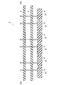
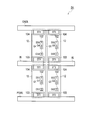
また、図16のXVIIa-XVIIa線に沿う模式的断面構造は、図17(a)に示すように表され、図16のXVIIb-XVIIb線に沿う模式的断面構造は、図17(b)に示すように表される。
また、図16のXVIIa-XVIIa線に沿う別の模式的断面構造は、図18(a)に示すように表され、図16のXVIIb-XVIIb線に沿う別の模式的断面構造は、図18(b)に示すように表される。
また、図16のXVIIa-XVIIa線に沿うさらに別の模式的断面構造は、図19(a)に示すように表され、図16のXVIIb-XVIIb線に沿うさらに別の模式的断面構造は、図19(b)に示すように表される。
また、電力系端子ST・DTは、図3(a)~図3(c)に示したように、樹脂層12の厚み方向に、所定の段差VD1・VD2・VD3をもって配置されており、図17の例は、図3(a)に示された所定の段差VD1を有する例に対応し、図18の例は、図3(b)に示された所定の段差VD2を有する例に対応し、図19の例は、図3(c)に示された所定の段差VD3を有する例に対応する。
すなわち、図3(a)に示された所定の段差VD1を有する例では、図17(a)に示すように、バスバー電極POWL・GNDLと共に、バスバー電極UL・VL・WLはストレートな電極構造を有する。
図3(b)に示された所定の段差VD2を有する例では、バスバー電極POWL・GNDLはストレートな電極構造を有するが、図18(a)に示すように、バスバー電極UL・VL・WLは所定の段差VD2の値が相対的に小さいために上方向に屈曲した電極構造を有する。
図3(c)に示された所定の段差VD3を有する例では、バスバー電極POWL・GNDLはストレートな電極構造を有するが、図19(a)に示すように、バスバー電極UL・VL・WLは所定の段差VD3の値が相対的に大きいために下方向に屈曲した電極構造を有する。
本実施の形態に係るストレート配線構造のパワーモジュール半導体装置2を6個配置して構成した3相交流インバータ装置4において、信号系端子SS・G・DSを非直線状に配置した例は、図20に示すように表される。
すなわち、本実施の形態に係るパワーモジュール半導体装置2においては、信号系端子DS・G・SSは、樹脂層12の主表面上に非直線状に配置されていても良い。または、信号系端子DS・G・SSは、樹脂層12の主表面上にランダムに配置されていても良い。
本実施の形態に係るパワーモジュール半導体装置2を複数個並列に配置したインバータ装置4は、図16および図20に示すように、パワーモジュール半導体装置2を複数個並列に配置し、各パワーモジュール半導体装置2の電力系端子ST・DTを、バスバー電極GNDL・POWLを介して相互に接続している。
また、本実施の形態に係るパワーモジュール半導体装置2を複数個並列に配置したインバータ装置4は、パワーモジュール半導体装置2のドレイン端子DTおよびソース端子STが、隣接するパワーモジュール半導体装置2のソース端子STおよびドレイン端子DTと互いに対向するように配置している。
そして、本実施の形態に係るパワーモジュール半導体装置2を複数個並列に配置したインバータ装置4は、複数のパワーモジュール半導体装置2において、ハーフブリッジを構成する第1トランジスタ・第2トランジスタ(Q1・Q4)・(Q2・Q5)・(Q3・Q6)を隣接させて配置し、かつ第1トランジスタのソース端子・ドレイン端子と第2トランジスタのドレイン端子・ソース端子とが互いに隣接するように配置している。
すなわち、第1トランジスタ・第2トランジスタ(Q1・Q4)のソース端子・ドレイン端子(ST1・DT4)、第1トランジスタ・第2トランジスタ(Q1・Q4)のドレイン端子・ソース端子(DT1・ST4)、第1トランジスタ・第2トランジスタ(Q2・Q5)のソース端子・ドレイン端子(ST2・DT5)、第1トランジスタ・第2トランジスタ(Q2・Q5)のドレイン端子・ソース端子(DT2・ST5)、第1トランジスタ・第2トランジスタ(Q3・Q6)のソース端子・ドレイン端子(ST3・DT6)、第1トランジスタ・第2トランジスタ(Q3・Q6)のドレイン端子・ソース端子(DT3・ST6)が、互いに隣接するように配置している。
本実施の形態に係るパワーモジュール半導体装置2においては、各組のパワーモジュール半導体装置2の電力系端子ST・DTを、バスバー電極UL・VL・WLを介して相互に接続することによって、3相交流用のインバータ装置4をコンパクトに構成可能である。
本実施の形態に係るパワーモジュール半導体装置2は、ストレート配線のモジュール構造において、段差端子構造を有するため、外部配線(バスバー配線)のインダクタンスLsを低くした配線を実現することができる。
本実施の形態に係るパワーモジュール半導体装置2は、ワンインワン構成において、ドレイン端子DTとソース端子STとを平面視矩形の樹脂層12の両端にストレート(直線的)に配置し、かつドレイン端子DTとソース端子STとの高さ位置に段差をつけることによって、モジュールの並列横並び配置により容易に3相交流インバータ装置(6 in 1)を構成可能である。
また、ドレイン端子DTとソース端子STとの高さ位置に段差を設けることで、モジュール間を配線するバスバー電極POWL・GNDL・UL・VL・WL同士の絶縁距離を容易に確保することができ、また、配線効率を良好にすることができる。
また、絶縁距離を確保するために配線(バスバー電極)を折り曲げ加工する構成に比べ、本実施の形態に係るパワーモジュール半導体装置2を適用した3相交流インバータ装置4では、配線長を低減可能であり、従来に比べて寄生インダクタンスLsを約10%低減することができる。モジュール端子に段差をつけることで外部配線(バスバーというモジュール同士を配線するもの)を曲げなくても済むためバスバーの配線長が短くできる。ここで、Lsは、バスバーの配線長の直列インダクタンス成分を表す。
[縦積み構造]
本実施の形態に係るパワーモジュール半導体装置2を6個配置して3相交流インバータ装置4を構成した各パワー端子間の接続配線(バスバー)電極(GNDL・POWL)も含む平面構成において、制御基板6および電源基板8を上部に配置した例は、図21に示すように表され、図21のXXII-XXII線に沿う模式的断面構造は、図22に示すように表される。
本実施の形態に係るパワーモジュール半導体装置2を6個配置して3相交流インバータ装置4を構成した各パワー端子間の接続配線(バスバー)電極(GNDL・POWL)も含む平面構成において、制御基板6および電源基板8を上部に配置した例は、図21に示すように表され、図21のXXII-XXII線に沿う模式的断面構造は、図22に示すように表される。
本実施の形態に係るパワーモジュール半導体装置2を6個配置して構成した3相交流インバータ装置4は、図21および図22に示すように、複数個並列に配置されたパワーモジュール半導体装置2上に配置され、パワーモジュール半導体装置2を制御する制御基板6と、複数個並列に配置されたパワーモジュール半導体装置2上に配置され、パワーモジュール半導体装置2および制御基板6に電源を供給する電源基板8とを備え、信号系端子DS・G・SSが延伸する垂直方向の長さは、制御基板6および電源基板8と接続可能な長さである。
本実施の形態に係るパワーモジュール半導体装置2を6個配置して構成した3相交流インバータ装置4上に制御基板6および電源基板8を配置した鳥瞰構成図は、図23に示すように表される。図23においては、6個のパワーモジュール半導体装置2の信号系端子(DS1・G1・SS1)・(DS2・G2・SS2)・(DS3・G3・SS3)・(DS4・G4・SS4)・(DS5・G5・SS5)・(DS6・G6・SS6)は、それぞれ制御基板6および電源基板8に対して垂直方向に接続されて、3相交流インバータ装置4を構成している。なお、図23においては、簡単化するために、制御基板6・電源基板8の詳細パターンは図示を省略している。また、図23においては、構造の詳細を明確にするために、パワーモジュール半導体装置2と制御基板6・電源基板8の縦方向の距離が相対的に長くなるように図示しているが、実際上は、距離を詰めて配置される。
本実施の形態に係るストレート配線構造のパワーモジュール半導体装置2を6個配置して構成した3相交流インバータ装置4においては、制御基板6、電源基板8、スナバコンデンサC(図示省略)などを縦積み構造に配置することが容易になり、システムのスリム化を図ることができる。
[フルブリッジインバータの構成]
本実施の形態に係るパワーモジュール半導体装置2を4個配置して構成したフルブリッジインバータ装置5の回路構成は、図24に示すように表される。
本実施の形態に係るパワーモジュール半導体装置2を4個配置して構成したフルブリッジインバータ装置5の回路構成は、図24に示すように表される。
また、本実施の形態に係るパワーモジュール半導体装置2を4個配置してフルブリッジインバータ装置5を構成した各パワー端子間の接続配線(バスバー)電極(GNDL・POWL)も含む平面構成は、図25に示すように表される。
本実施の形態に係るパワーモジュール半導体装置2を4個配置して構成したフルブリッジインバータ装置5においても、制御基板6(図示省略)、電源基板8(図示省略)、スナバコンデンサC(図示省略)などを縦積み構造に配置することが容易であり、システムのスリム化を図ることができる。
[半導体デバイスの構成例]
本実施の形態に係るパワーモジュール半導体装置2に適用する半導体デバイス100(Q)の例として、SiC MOSFETの模式的断面構造は、図26に示すように、n-高抵抗層からなるSiC半導体基板26と、SiC半導体基板26の表面側に形成されたpベース領域28と、pベース領域28の表面に形成されたソース領域30と、pベース領域28間のSiC半導体基板26の表面上に配置されたゲート絶縁膜32と、ゲート絶縁膜32上に配置されたゲート電極38と、ソース領域30およびpベース領域28に接続されたソース電極34と、SiC半導体基板26の表面と反対側の裏面に配置されたn+ドレイン領域24と、n+ドレイン領域24に接続されたドレイン電極36とを備える。
本実施の形態に係るパワーモジュール半導体装置2に適用する半導体デバイス100(Q)の例として、SiC MOSFETの模式的断面構造は、図26に示すように、n-高抵抗層からなるSiC半導体基板26と、SiC半導体基板26の表面側に形成されたpベース領域28と、pベース領域28の表面に形成されたソース領域30と、pベース領域28間のSiC半導体基板26の表面上に配置されたゲート絶縁膜32と、ゲート絶縁膜32上に配置されたゲート電極38と、ソース領域30およびpベース領域28に接続されたソース電極34と、SiC半導体基板26の表面と反対側の裏面に配置されたn+ドレイン領域24と、n+ドレイン領域24に接続されたドレイン電極36とを備える。
図26では、半導体デバイス100は、プレーナゲート型nチャネル縦型SiC MOSFETで構成されているが、トレンチゲート型nチャネル縦型SiC MOSFETなどで構成されていても良い。
また、本実施の形態に係るパワーモジュール半導体装置2に適用する半導体デバイス100には、SiC MOSFETの代わりに、GaN系FETやSiC基板を用いたIGBTなどを適用することもできる。
本実施の形態に係るパワーモジュール半導体装置2に適用する半導体デバイス100には、SiC系、GaN系、もしくはAlN系のいずれかのパワーデバイスを適用可能である。
さらには、本実施の形態に係るパワーモジュール半導体装置2に適用する半導体デバイス100には、バンドギャップエネルギーが、例えば、1.1eV~8eVのワイドギャップと称される半導体基板を用いたMOSトランジスタなどを用いることができる。
本実施の形態に係るパワーモジュール半導体装置2に適用する半導体デバイス100の例であって、ソースパッド電極SP、ゲートパッド電極GPを含むSiC MOSFETの模式的断面構造は、図27に示すように表される。ゲートパッド電極GPは、ゲート絶縁膜32上に配置されたゲート電極38に接続され、ソースパッド電極SPは、ソース領域30およびpベース領域28に接続されたソース電極34に接続される。
また、ゲートパッド電極GPおよびソースパッド電極SPは、図27に示すように、半導体デバイス100の表面を覆うパッシベーション用の層間絶縁膜44上に配置される。
なお、ゲートパッド電極GPおよびソースパッド電極SPの下方のSiC半導体基板26内には、図27の構成例では図示を省略しているが、図26の中央部と同様に、微細構造のトランジスタ構造が形成されていても良い。
さらに、図27に示すように、中央部のトランジスタ構造においても、パッシベーション用の層間絶縁膜44上にソースパッド電極SPが延在して配置されていても良い。
本実施の形態に係るパワーモジュール半導体装置2において、電源端子PLと接地端子NL間にスナバコンデンサCを接続した回路構成は、図28に示すように表される。本実施の形態に係るパワーモジュール半導体装置2を蓄電池Eと接続する際、接続ラインの有するインダクタンスLによって、SiC系デバイスのスイッチング速度が速いため、大きなサージ電圧Ldi/dtを生ずる。例えば、電流変化di=300A、スイッチングに伴う時間変化dt=100nsecとすると、di/dt=3×109 (A/s)となる。インダクタンスLの値により、サージ電圧Ldi/dtの値は変化するが、蓄電池Eにこのサージ電圧Ldi/dtが重畳される。電源端子PLと接地端子NLとの間に接続されるスナバコンデンサCによって、このサージ電圧Ldi/dtを吸収することができる。
[パワーモジュール半導体装置を適用した応用例]
次に、図29を参照して、本実施の形態に係るパワーモジュール半導体装置2を用いて構成した3相交流インバータについて説明する。
次に、図29を参照して、本実施の形態に係るパワーモジュール半導体装置2を用いて構成した3相交流インバータについて説明する。
図29に示すように、3相交流インバータは、ゲートドライブ部50と、ゲートドライブ部50に接続されたパワーモジュール部52と、3相交流モータ部54とを備える。パワーモジュール部52は、3相交流モータ部54のU相、V相、W相に対応して、U相、V相、W相のインバータが接続されている。ここで、ゲートドライブ部50は、図29では、SiC MOSFET Q1・Q4に接続されている。図示は省略しているが、同様に、SiC MOSFET Q2・Q5、およびSiC MOSFET Q3・Q6にも接続されている。
パワーモジュール部52は、蓄電池(E)46の接続されたコンバータ48が接続されたプラス端子(+)とマイナス端子(-)との間に、インバータ構成のSiC MOSFET Q1・Q4、Q2・Q5、およびQ3・Q6が接続されている。さらに、SiC MOSFET Q1~Q6のソース・ドレイン間には、ダイオードD1~D6がそれぞれ逆並列に接続されている。
本実施の形態に係るパワーモジュール半導体装置2では、図29のU相部分に対応する単相インバータの構造について説明されていたが、V相、W相に対応しても同様に形成して、3相パワーモジュール部52を形成することもできる。
[パワーモジュール半導体装置の製造方法]
本実施の形態に係るパワーモジュール半導体装置2の製造方法において、電力系端子ST・DTおよび信号系端子DS・G・SSの半田付け工程に使用するカーボン治具400の模式的平面構成は、図30(a)に示すように表される。
本実施の形態に係るパワーモジュール半導体装置2の製造方法において、電力系端子ST・DTおよび信号系端子DS・G・SSの半田付け工程に使用するカーボン治具400の模式的平面構成は、図30(a)に示すように表される。
カーボン治具400は、図30(b)に示すように、中央に基板挿入部402、左右両端に凹部形状のドレイン端子DT裁置部401a・ソース端子ST裁置部401bを備える。
また、パワーモジュール半導体装置2をカーボン治具400に搭載し、パワーモジュール半導体装置2を搭載したカーボン治具400をホットプレート403上に搭載し、カーボン治具400の長手方向で切った模式的断面構造は、図31に示すように表される。
なお、図31は、図30(b)のXXXI-XXXIに沿う模式的断面構造に対応しており、電力系端子ST・DTおよび信号系端子DS・G・SSの半田付け工程を実施した様子を示している。ただし、信号系端子DS・G・SSは、破線により、信号系端子DS・G・SSの相対的な位置を示している。
ホットプレート403を加熱することによって、信号系端子DSを第1パターン10a(D)に、信号系端子G・SSを電極パターンGSP・SSPに、それぞれ半田付けすることができる。また、電力系端子ST・DTを、パワーモジュール半導体装置2の柱状接続電極18n・第1パターン10a(D)に半田付けすることができる。ここで、高融点半田を使用する場合には、ホットプレート403を、例えば、約340℃~360℃程度に加熱する。
なお、図32に示されるように、半田付けされた信号系端子DSには1端子ホルダ101が、また、半田付けされた信号系端子G・SSには2端子ホルダ102が、それぞれ係合された後、封止の工程が行われる。
本実施の形態に係るパワーモジュール半導体装置2の製造方法においては、図30~図31に示された構造のカーボン治具400を使用することによって、電力系端子ST・DTおよび絶縁基板10の平行性を確保することができる。
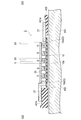
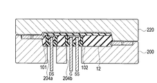
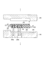
また、本実施の形態に係るパワーモジュール半導体装置2の製造方法において、トランスファモールド成形工程を説明する模式的断面構造は、図32~図34に示すように表される。
すなわち、図32~図34には、製造工程を経て信号系端子DS・G・SSに1端子ホルダ101・2端子ホルダ102を取り付けた構造体の上下を反対にし、上金型(第2の金型)220および下金型(第1の金型)200によって挟み込み、モールド樹脂を封入して樹脂層12を形成後、上金型220および下金型200を取り外した様子が示されている。なお、図32~図34において、202・203は、本体載置部・端子載置部、204a・204bは、信号系端子DS・G・SSの収容部、223は、樹脂注入部である。
本実施の形態に係るパワーモジュール半導体装置2の製造方法において、モールド面よりも高さda(α)の分だけ背高になるように取り付けられた1端子ホルダ101・2端子ホルダ102は、構造体の上下を上金型220および下金型200によって挟み込む際に下金型200によって垂直方向に押圧される。そして、この状態、つまり1端子ホルダ101・2端子ホルダ102が下金型200に確実に当接されて互いに密着された状態で、樹脂注入部223への樹脂の注入が実行される。
本実施の形態に係るパワーモジュール半導体装置2の製造方法においては、図32~図34に示される上金型220および下金型200を使用することによって、下金型200が1端子ホルダ101・2端子ホルダ102と密着されるので樹脂漏れなどを招いたりすることなく、電力系端子ST・DTの段差端子構造が実現されている。
本実施の形態に係るパワーモジュール半導体装置2によれば、信号系端子DS・G・SSが垂直方向に突き出した状態で1端子ホルダ101・2端子ホルダ102によりサポートされているので、モールド後に信号系端子DS・G・SSの曲げや絶縁確保の工程を追加する必要がなく、工程数の削減および故障のリスクを低減できる。
特に、信号系端子DS・G・SSをソケットに圧入する際の荷重応力がパワーモジュール半導体装置2に加えられたり、長期の使用中に振動などにより信号系端子DS・G・SSがパワーモジュール半導体装置2より抜けたりするのを防止できる。
[実施の他の形態]
[パワーモジュール半導体装置の構成]
図35に示すように、本実施の他の形態に係るパワーモジュール半導体装置2Aにおいては、さらに、電力系端子ST・DTが絶縁基板10の主表面に対して垂直方向に延伸して配置されてなる構成とされている。
[パワーモジュール半導体装置の構成]
図35に示すように、本実施の他の形態に係るパワーモジュール半導体装置2Aにおいては、さらに、電力系端子ST・DTが絶縁基板10の主表面に対して垂直方向に延伸して配置されてなる構成とされている。
また、本実施の他の形態に係るパワーモジュール半導体装置2Aにおいて、垂直方向に配置された電力系端子DTは1端子ホルダ(第2の係止部材)103によって、垂直方向に配置された電力系端子STは1端子ホルダ(第2の係止部材)104によって、それぞれ係止されるようにして保持されている。1端子ホルダ103・104としては、寸法以外は、1端子ホルダ101と構成が同一のものを用いることができる。
本実施の他の形態に係るパワーモジュール半導体装置2Aの構成によれば、信号系端子DS・G・SSのみならず、電力系端子ST・DTに関しても、圧入時の荷重応力による破損を防いだり、使用中の振動などによる端子抜けを防止できる。
[パワーモジュール半導体装置を適用した応用例]
図36には、本実施の他の形態に係るパワーモジュール半導体装置2Aを6個並列に配置して3相交流インバータ装置4Aを構成した平面構成が示されている。また、図37には、本実施の他の形態に係るパワーモジュール半導体装置2Aを4個並列に配置してフルブリッジインバータ装置5Aを構成した平面構成が示されている。
図36には、本実施の他の形態に係るパワーモジュール半導体装置2Aを6個並列に配置して3相交流インバータ装置4Aを構成した平面構成が示されている。また、図37には、本実施の他の形態に係るパワーモジュール半導体装置2Aを4個並列に配置してフルブリッジインバータ装置5Aを構成した平面構成が示されている。
本実施の他の形態に係るパワーモジュール半導体装置2Aによれば、信号系端子DS・G・SSと同様に、電力系端子ST・DTが垂直方向に突き出した状態で1端子ホルダ103・104によりサポートされているので、より小型化が可能であり、3相交流インバータ装置4Aおよびフルブリッジインバータ装置5Aを、より一層コンパクトに構成できる。
すなわち、本実施の他の形態に係るパワーモジュール半導体装置2Aにおいては、樹脂層12の外周に信号系端子SS・G・DSおよび電力系端子ST・DTを配置していないので、図36および図37に示したように、並列配置してもパワーモジュール間距離をさらに詰めることができる。
特に、端子DS・G・SS・ST・DTの垂直方向への引き出しは、モジュール内での配線の引き回しを短縮化できるなど、耐ノイズ性や損失の低減に寄与するため、高電圧分野への応用などが期待される。
以上説明したように、小型化が可能であり、荷重応力による破損や端子抜けを改善できるパワーモジュール半導体装置およびその製造方法、およびこのパワーモジュール半導体装置を有するインバータ装置を提供することができる。
[その他の実施の形態]
上記のように、いくつかの実施の形態を記載したが、開示の一部をなす論述および図面は例示的なものであり、実施の各形態を限定するものであると理解すべきではない。この開示から当業者には様々な代替実施の形態、実施例および運用技術が明らかとなろう。
上記のように、いくつかの実施の形態を記載したが、開示の一部をなす論述および図面は例示的なものであり、実施の各形態を限定するものであると理解すべきではない。この開示から当業者には様々な代替実施の形態、実施例および運用技術が明らかとなろう。
このように、本実施の各形態は、ここでは記載していない様々な形態などを含む。
本実施の形態に係るパワーモジュール半導体装置は、SiCパワー半導体モジュールなどのパワーデバイス全般に利用可能であり、特に、小型・軽量化が求められている分野、車載・太陽電池・産業機器・民生機器向けのインバータ、コンバータなどの幅広い応用分野に適用可能である。
2、2A、2B、2C…パワーモジュール半導体装置
3a、3b、3c…半田層
4、4A、5、5A…インバータ装置
6…制御基板
8…電源基板
10…絶縁基板
10a、10b…銅プレート層
10a(D)…第1パターン
10a(S)…第2パターン
12…樹脂層
18n…柱状接続電極
20…柱状電極
22…上面板電極
24…n+ ドレイン領域
26…SiC半導体基板
28…pベース領域
30…ソース領域
32…ゲート絶縁膜
34…ソース電極
36…ドレイン電極
38…ゲート電極
44…層間絶縁膜
46…蓄電池(E)
48…コンバータ
50…ゲートドライブ部
52…パワーモジュール部
54…3相交流モータ部
100、Q、Q1~Q6…半導体デバイス(SiC MOSFET、半導体チップ)
101…1端子ホルダ(第1の係止部材)
101a…樹脂充填部
101b…開口部
101c…送入口(送入穴)
101d…送出口(送出穴)
102…2端子ホルダ(第1の係止部材)
102a…樹脂充填部
102b、102c…開口部
102d…送入口(送入穴)
102e…送出口(送出穴)
103、104…1端子ホルダ(第2の係止部材)
200…下金型
204a・204b…収容部
220…上金型
223…樹脂注入部
400…カーボン治具
D1~D6、DI…ダイオード
GP…ゲートパッド電極
SP…ソースパッド電極
DT、DT1、DT2、DT3、DT4、DT5、DT6…ドレイン端子(電力系端子)
ST、ST1、ST2、ST3、ST4、ST5、ST6…ソース端子(電力系端子)
POWL、GNDL、UL、VL、WL…バスバー電極
O、U、V、W…出力端子
G、G1~G6…ゲート信号端子(信号系端子)
SS、SS1~SS6…ソースセンス端子(信号系端子)
DS、DS1~DS6…ドレインセンス端子(信号系端子)
GSP…ゲート信号電極パターン
SSP…ソースセンス電極パターン
3a、3b、3c…半田層
4、4A、5、5A…インバータ装置
6…制御基板
8…電源基板
10…絶縁基板
10a、10b…銅プレート層
10a(D)…第1パターン
10a(S)…第2パターン
12…樹脂層
18n…柱状接続電極
20…柱状電極
22…上面板電極
24…n+ ドレイン領域
26…SiC半導体基板
28…pベース領域
30…ソース領域
32…ゲート絶縁膜
34…ソース電極
36…ドレイン電極
38…ゲート電極
44…層間絶縁膜
46…蓄電池(E)
48…コンバータ
50…ゲートドライブ部
52…パワーモジュール部
54…3相交流モータ部
100、Q、Q1~Q6…半導体デバイス(SiC MOSFET、半導体チップ)
101…1端子ホルダ(第1の係止部材)
101a…樹脂充填部
101b…開口部
101c…送入口(送入穴)
101d…送出口(送出穴)
102…2端子ホルダ(第1の係止部材)
102a…樹脂充填部
102b、102c…開口部
102d…送入口(送入穴)
102e…送出口(送出穴)
103、104…1端子ホルダ(第2の係止部材)
200…下金型
204a・204b…収容部
220…上金型
223…樹脂注入部
400…カーボン治具
D1~D6、DI…ダイオード
GP…ゲートパッド電極
SP…ソースパッド電極
DT、DT1、DT2、DT3、DT4、DT5、DT6…ドレイン端子(電力系端子)
ST、ST1、ST2、ST3、ST4、ST5、ST6…ソース端子(電力系端子)
POWL、GNDL、UL、VL、WL…バスバー電極
O、U、V、W…出力端子
G、G1~G6…ゲート信号端子(信号系端子)
SS、SS1~SS6…ソースセンス端子(信号系端子)
DS、DS1~DS6…ドレインセンス端子(信号系端子)
GSP…ゲート信号電極パターン
SSP…ソースセンス電極パターン
Claims (25)
- 絶縁基板と、
前記絶縁基板上に配置されたプレート層の第1パターンと、
前記第1パターン上に配置された半導体デバイスと、
前記半導体デバイスと電気的に接続された電力系端子と、
前記半導体デバイスと電気的に接続されると共に、前記絶縁基板の主表面に対して垂直方向に延伸して配置された信号系端子と、
前記信号系端子を係止する第1の係止部材と、
前記第1の係止部材の一部を露出させるようにして、前記半導体デバイスおよび前記絶縁基板を被覆する樹脂層と
を備えることを特徴とするパワーモジュール半導体装置。 - 前記第1の係止部材は、所定の耐熱性を有することを特徴とする請求項1に記載のパワーモジュール半導体装置。
- 前記第1の係止部材は、その内部に樹脂を充填させるための送入穴と送出穴とを有し、前記送入穴は前記送出穴よりも大きいことを特徴とする請求項1または2に記載のパワーモジュール半導体装置。
- 前記第1の係止部材は、PPSもしくはPEEKのプラスチックであることを特徴とする請求項1~3のいずれか1項に記載のパワーモジュール半導体装置。
- 前記樹脂層は長手方向と短手方向とを有する平面視矩形状をしており、
前記電力系端子は、前記樹脂層の主表面と平行に、前記樹脂層の長手方向に沿って、前記樹脂層の対向する両側面から互いに逆方向に延伸して配置され、ストレート配線構造を有することを特徴とする請求項1に記載のパワーモジュール半導体装置。 - 前記電力系端子は、前記樹脂層の厚み方向に、所定の段差をもって配置されることを特徴とする請求項1~5のいずれか1項に記載のパワーモジュール半導体装置。
- 前記信号系端子は、前記樹脂層の主表面上に直線状に配置されることを特徴とする請求項1~6のいずれか1項に記載のパワーモジュール半導体装置。
- 前記信号系端子は、前記樹脂層の主表面上に非直線状に配置されることを特徴とする請求項1~6のいずれか1項に記載のパワーモジュール半導体装置。
- 前記半導体デバイスは、ソース電極、ドレイン電極およびゲート電極を有するMOSFETであることを特徴とする請求項1~6のいずれか1項に記載のパワーモジュール半導体装置。
- 前記信号系端子は、前記ゲート電極につながるゲート信号端子およびセンサ用端子を備え、
前記センサ用端子は、前記ソース電極につながるソースセンス端子および前記MOSFETと同じ構造で、前記ドレイン電極および前記ゲート電極とそれぞれ共通に接続されたセンス用MOSFETのソース電極につながるドレインセンス端子を備えることを特徴とする請求項9に記載のパワーモジュール半導体装置。 - 前記ドレインセンス端子は、前記第1パターンに半田付けにより接続され、
前記ゲート信号端子および前記ソースセンス端子は、前記絶縁基板上に前記半導体デバイスに隣接して配置された電極パターンに半田付けにより接続されることを特徴とする請求項10に記載のパワーモジュール半導体装置。 - 前記電力系端子は、前記半導体デバイスのドレイン電極に接続されたドレイン電極端子と、前記半導体デバイスのソースパッド電極に接続されたソース電極端子とを備えることを特徴とする請求項9~11のいずれか1項に記載のパワーモジュール半導体装置。
- 前記絶縁基板は、セラミック基板で構成されることを特徴とする請求項1~12のいずれか1項に記載のパワーモジュール半導体装置。
- 前記絶縁基板上に配置されたプレート層の第2パターンと、
前記半導体デバイス上に配置された柱状電極と、
前記柱状電極上に配置された上面板電極と、
前記第1パターン上に配置された第1の電力系端子と、
前記第2パターン上に配置され、かつ前記上面板電極と接続された柱状接続電極と、
前記柱状接続電極に接続された第2の電力系端子と
を備えることを特徴とする請求項1に記載のパワーモジュール半導体装置。 - 前記半導体デバイスは、ソース電極、ドレイン電極およびゲート電極を有するMOSFETであり、
前記第1の電力系端子は、前記ソース電極に接続され、前記第2の電力系端子は、前記ドレイン電極に接続されたことを特徴とする請求項14に記載のパワーモジュール半導体装置。 - 前記樹脂層は、エポキシ系樹脂もしくはシリコーン系樹脂でトランスファモールド成形されたことを特徴とする請求項1~15のいずれか1項に記載のパワーモジュール半導体装置。
- 前記セラミック基板は、Al2 O3 、AlN、SiN、AlSiC、もしくは少なくとも表面が絶縁性のSiCあることを特徴とする請求項13に記載のパワーモジュール半導体装置。
- 前記半導体デバイスは、SiC系、GaN系、もしくはAlN系のいずれかのパワーデバイスであることを特徴とする請求項1~17のいずれか1項に記載のパワーモジュール半導体装置。
- 前記電力系端子は、前記絶縁基板の主表面に対して垂直方向に延伸して配置されることを特徴とする請求項1に記載のパワーモジュール半導体装置。
- 前記電力系端子を係止する第2の係止部材を、さらに備えることを特徴とする請求項19に記載のパワーモジュール半導体装置。
- 前記第2の係止部材は、その一部が露出されるようにして前記樹脂層により被覆されることを特徴とする請求項20に記載のパワーモジュール半導体装置。
- 請求項1~21に記載のパワーモジュール半導体装置を複数有し、前記樹脂層は長手方向と短手方向とを有する平面視矩形状をしており、各パワーモジュール半導体装置をその短手方向に近接して配置したことを特徴とするインバータ装置。
- 絶縁基板上に配置されたプレート層の第1パターン上に配置された半導体デバイスと、前記半導体デバイスと電気的に接続された電力系端子と、前記半導体デバイスと電気的に接続されると共に、前記絶縁基板の主表面に対して垂直方向に延伸して配置された信号系端子と、前記信号系端子を係止する第1の係止部材と、を含んで、前記絶縁基板の垂直方向に対向する両表面側を第1の金型および第2の金型により保持する第1の工程と、
前記第1の金型および前記第2の金型内に樹脂を充填させ、前記第1の係止部材の一部を露出させるようにして、前記半導体デバイスおよび前記絶縁基板を被覆する樹脂層を形成する第2の工程と
を有することを特徴とするパワーモジュール半導体装置の製造方法。 - 前記第1の係止部材は、その垂直方向の主表面が、前記樹脂によって形成される前記樹脂層の垂直方向の主表面より突出するように設けられており、
前記第1の工程において、前記第1の金型および前記第2の金型により前記絶縁基板を保持する際、前記第1の係止部材が前記第1の金型によって垂直方向に押圧されることを特徴とする請求項23に記載のパワーモジュール半導体装置の製造方法。 - 前記電力系端子は、前記絶縁基板の主表面に対して垂直方向に延伸して配置され、かつ前記電力系端子を係止する第2の係止部材をさらに備え、
前記第2の係止部材は、その垂直方向の主表面が、前記樹脂によって形成される前記樹脂層の垂直方向の主表面より突出するように設けられており、
前記第1の工程において、前記第1の金型および前記第2の金型により前記絶縁基板を保持する際、前記第2の係止部材が前記第1の金型によって垂直方向に押圧されることを特徴とする請求項23に記載のパワーモジュール半導体装置の製造方法。
Applications Claiming Priority (2)
| Application Number | Priority Date | Filing Date | Title |
|---|---|---|---|
| JP2015-115587 | 2015-06-08 | ||
| JP2015115587A JP6600172B2 (ja) | 2015-06-08 | 2015-06-08 | パワーモジュール半導体装置およびその製造方法、およびインバータ装置 |
Publications (1)
| Publication Number | Publication Date |
|---|---|
| WO2016199635A1 true WO2016199635A1 (ja) | 2016-12-15 |
Family
ID=57503736
Family Applications (1)
| Application Number | Title | Priority Date | Filing Date |
|---|---|---|---|
| PCT/JP2016/066157 Ceased WO2016199635A1 (ja) | 2015-06-08 | 2016-06-01 | パワーモジュール半導体装置およびその製造方法、およびインバータ装置 |
Country Status (2)
| Country | Link |
|---|---|
| JP (1) | JP6600172B2 (ja) |
| WO (1) | WO2016199635A1 (ja) |
Cited By (6)
| Publication number | Priority date | Publication date | Assignee | Title |
|---|---|---|---|---|
| CN110364512A (zh) * | 2018-04-11 | 2019-10-22 | 半导体元件工业有限责任公司 | 用以防止短路事件的半导体功率模块 |
| WO2020196699A1 (ja) * | 2019-03-27 | 2020-10-01 | 福島SiC応用技研株式会社 | パワー基板とそれを備えた高電圧モジュール |
| US10847437B2 (en) * | 2018-10-10 | 2020-11-24 | Mitsubishi Electric Corporation | Semiconductor device |
| US20210092882A1 (en) * | 2019-09-25 | 2021-03-25 | Audi Ag | Molded power module with integrated exciter circuit |
| WO2021059947A1 (ja) * | 2019-09-27 | 2021-04-01 | ローム株式会社 | 半導体装置 |
| CN116420223A (zh) * | 2020-10-20 | 2023-07-11 | 三菱电机株式会社 | 半导体装置 |
Families Citing this family (6)
| Publication number | Priority date | Publication date | Assignee | Title |
|---|---|---|---|---|
| US11482479B2 (en) | 2017-04-24 | 2022-10-25 | Rohm Co., Ltd. | Semiconductor device |
| CN109923667B (zh) | 2017-10-10 | 2022-11-25 | 新电元工业株式会社 | 半导体装置、以及电力转换装置 |
| US11502014B2 (en) * | 2018-09-19 | 2022-11-15 | Rohm Co., Ltd. | Semiconductor device |
| US20210384109A1 (en) * | 2018-10-18 | 2021-12-09 | Nissan Arc, Ltd. | Semiconductor device and method of manufacturing the same |
| KR102703392B1 (ko) | 2019-11-25 | 2024-09-04 | 현대자동차주식회사 | 전력모듈 및 전력모듈에 적용되는 기판 구조 |
| JP2025527352A (ja) * | 2022-08-18 | 2025-08-20 | ヒタチ・エナジー・リミテッド | 半導体パワーモジュールおよび半導体パワーモジュールを製造するための方法 |
Citations (4)
| Publication number | Priority date | Publication date | Assignee | Title |
|---|---|---|---|---|
| JP2009200416A (ja) * | 2008-02-25 | 2009-09-03 | Mitsubishi Electric Corp | 半導体装置および半導体装置の製造方法 |
| JP2010129795A (ja) * | 2008-11-28 | 2010-06-10 | Mitsubishi Electric Corp | 電力用半導体モジュール |
| JP2012248907A (ja) * | 2012-09-21 | 2012-12-13 | Mitsubishi Electric Corp | 電力半導体装置 |
| WO2014046058A1 (ja) * | 2012-09-20 | 2014-03-27 | ローム株式会社 | パワーモジュール半導体装置およびインバータ装置、およびパワーモジュール半導体装置の製造方法、および金型 |
-
2015
- 2015-06-08 JP JP2015115587A patent/JP6600172B2/ja active Active
-
2016
- 2016-06-01 WO PCT/JP2016/066157 patent/WO2016199635A1/ja not_active Ceased
Patent Citations (4)
| Publication number | Priority date | Publication date | Assignee | Title |
|---|---|---|---|---|
| JP2009200416A (ja) * | 2008-02-25 | 2009-09-03 | Mitsubishi Electric Corp | 半導体装置および半導体装置の製造方法 |
| JP2010129795A (ja) * | 2008-11-28 | 2010-06-10 | Mitsubishi Electric Corp | 電力用半導体モジュール |
| WO2014046058A1 (ja) * | 2012-09-20 | 2014-03-27 | ローム株式会社 | パワーモジュール半導体装置およびインバータ装置、およびパワーモジュール半導体装置の製造方法、および金型 |
| JP2012248907A (ja) * | 2012-09-21 | 2012-12-13 | Mitsubishi Electric Corp | 電力半導体装置 |
Cited By (11)
| Publication number | Priority date | Publication date | Assignee | Title |
|---|---|---|---|---|
| CN110364512A (zh) * | 2018-04-11 | 2019-10-22 | 半导体元件工业有限责任公司 | 用以防止短路事件的半导体功率模块 |
| US10847437B2 (en) * | 2018-10-10 | 2020-11-24 | Mitsubishi Electric Corporation | Semiconductor device |
| WO2020196699A1 (ja) * | 2019-03-27 | 2020-10-01 | 福島SiC応用技研株式会社 | パワー基板とそれを備えた高電圧モジュール |
| JP2020161719A (ja) * | 2019-03-27 | 2020-10-01 | 福島SiC応用技研株式会社 | パワー基板とそれを備えた高電圧モジュール |
| JP7170272B2 (ja) | 2019-03-27 | 2022-11-14 | ネクスファイ・テクノロジー株式会社 | パワー基板とそれを備えた高電圧モジュール |
| US12022604B2 (en) | 2019-03-27 | 2024-06-25 | NaxFI Technology Inc. | Power substrate and high-voltage module equipped with same |
| US20210092882A1 (en) * | 2019-09-25 | 2021-03-25 | Audi Ag | Molded power module with integrated exciter circuit |
| US11659698B2 (en) * | 2019-09-25 | 2023-05-23 | Audi Ag | Molded power module with integrated exciter circuit |
| WO2021059947A1 (ja) * | 2019-09-27 | 2021-04-01 | ローム株式会社 | 半導体装置 |
| JP7596283B2 (ja) | 2019-09-27 | 2024-12-09 | ローム株式会社 | 半導体装置 |
| CN116420223A (zh) * | 2020-10-20 | 2023-07-11 | 三菱电机株式会社 | 半导体装置 |
Also Published As
| Publication number | Publication date |
|---|---|
| JP2017005043A (ja) | 2017-01-05 |
| JP6600172B2 (ja) | 2019-10-30 |
Similar Documents
| Publication | Publication Date | Title |
|---|---|---|
| JP6600172B2 (ja) | パワーモジュール半導体装置およびその製造方法、およびインバータ装置 | |
| US11973007B2 (en) | Power module semiconductor device and inverter equipment, and fabrication method of the power module semiconductor device, and metallic mold | |
| JP6503097B2 (ja) | パワーモジュール半導体装置 | |
| US10861833B2 (en) | Semiconductor device | |
| CN104412383B (zh) | 半导体装置以及半导体装置的连接构造 | |
| CN109427705B (zh) | 电子装置 | |
| CN104517954B (zh) | 在两个衬底之间具有半导体芯片的晶体管布置 | |
| CN109801898B (zh) | 具有多个模塑料的功率封装 | |
| CN101752358B (zh) | 带有整合旁路电容器的紧密半导体封装及其方法 | |
| US10903138B2 (en) | Semiconductor device and method of manufacturing the same | |
| CN110783283A (zh) | 具有对称布置的功率连接端的半导体封装及其制造方法 | |
| CN118299357B (zh) | 一种塑封boost半导体模块及封装结构 | |
| CN108122896A (zh) | 一种适合高频应用的薄型功率模块 | |
| JP2014120638A (ja) | パワーモジュール半導体装置およびその製造方法 | |
| JP2018107481A (ja) | パワーモジュール半導体装置 | |
| CN118899289B (zh) | 一种塑封功率模块结构 | |
| WO2024203278A1 (ja) | 半導体モジュールおよび車両 | |
| JP2024127545A (ja) | 半導体装置 | |
| CN118899288B (zh) | 一种塑封功率模块结构 | |
| US20250014972A1 (en) | Package with clip directly connected to oblong electric connection element extending along mounting base | |
| EP4639630A1 (en) | High power density flip chip semiconductor packaging |
Legal Events
| Date | Code | Title | Description |
|---|---|---|---|
| 121 | Ep: the epo has been informed by wipo that ep was designated in this application |
Ref document number: 16807342 Country of ref document: EP Kind code of ref document: A1 |
|
| NENP | Non-entry into the national phase |
Ref country code: DE |
|
| 122 | Ep: pct application non-entry in european phase |
Ref document number: 16807342 Country of ref document: EP Kind code of ref document: A1 |