WO2016190429A1 - 光学薄膜製造方法、光学フィルム製造方法 - Google Patents
光学薄膜製造方法、光学フィルム製造方法 Download PDFInfo
- Publication number
- WO2016190429A1 WO2016190429A1 PCT/JP2016/065790 JP2016065790W WO2016190429A1 WO 2016190429 A1 WO2016190429 A1 WO 2016190429A1 JP 2016065790 W JP2016065790 W JP 2016065790W WO 2016190429 A1 WO2016190429 A1 WO 2016190429A1
- Authority
- WO
- WIPO (PCT)
- Prior art keywords
- thin film
- optical
- optical thin
- flow rate
- value
- Prior art date
- Legal status (The legal status is an assumption and is not a legal conclusion. Google has not performed a legal analysis and makes no representation as to the accuracy of the status listed.)
- Ceased
Links
Images





Classifications
-
- C—CHEMISTRY; METALLURGY
- C23—COATING METALLIC MATERIAL; COATING MATERIAL WITH METALLIC MATERIAL; CHEMICAL SURFACE TREATMENT; DIFFUSION TREATMENT OF METALLIC MATERIAL; COATING BY VACUUM EVAPORATION, BY SPUTTERING, BY ION IMPLANTATION OR BY CHEMICAL VAPOUR DEPOSITION, IN GENERAL; INHIBITING CORROSION OF METALLIC MATERIAL OR INCRUSTATION IN GENERAL
- C23C—COATING METALLIC MATERIAL; COATING MATERIAL WITH METALLIC MATERIAL; SURFACE TREATMENT OF METALLIC MATERIAL BY DIFFUSION INTO THE SURFACE, BY CHEMICAL CONVERSION OR SUBSTITUTION; COATING BY VACUUM EVAPORATION, BY SPUTTERING, BY ION IMPLANTATION OR BY CHEMICAL VAPOUR DEPOSITION, IN GENERAL
- C23C14/00—Coating by vacuum evaporation, by sputtering or by ion implantation of the coating forming material
- C23C14/22—Coating by vacuum evaporation, by sputtering or by ion implantation of the coating forming material characterised by the process of coating
- C23C14/54—Controlling or regulating the coating process
- C23C14/542—Controlling the film thickness or evaporation rate
- C23C14/545—Controlling the film thickness or evaporation rate using measurement on deposited material
- C23C14/547—Controlling the film thickness or evaporation rate using measurement on deposited material using optical methods
-
- C—CHEMISTRY; METALLURGY
- C23—COATING METALLIC MATERIAL; COATING MATERIAL WITH METALLIC MATERIAL; CHEMICAL SURFACE TREATMENT; DIFFUSION TREATMENT OF METALLIC MATERIAL; COATING BY VACUUM EVAPORATION, BY SPUTTERING, BY ION IMPLANTATION OR BY CHEMICAL VAPOUR DEPOSITION, IN GENERAL; INHIBITING CORROSION OF METALLIC MATERIAL OR INCRUSTATION IN GENERAL
- C23C—COATING METALLIC MATERIAL; COATING MATERIAL WITH METALLIC MATERIAL; SURFACE TREATMENT OF METALLIC MATERIAL BY DIFFUSION INTO THE SURFACE, BY CHEMICAL CONVERSION OR SUBSTITUTION; COATING BY VACUUM EVAPORATION, BY SPUTTERING, BY ION IMPLANTATION OR BY CHEMICAL VAPOUR DEPOSITION, IN GENERAL
- C23C14/00—Coating by vacuum evaporation, by sputtering or by ion implantation of the coating forming material
- C23C14/06—Coating by vacuum evaporation, by sputtering or by ion implantation of the coating forming material characterised by the coating material
- C23C14/08—Oxides
-
- C—CHEMISTRY; METALLURGY
- C23—COATING METALLIC MATERIAL; COATING MATERIAL WITH METALLIC MATERIAL; CHEMICAL SURFACE TREATMENT; DIFFUSION TREATMENT OF METALLIC MATERIAL; COATING BY VACUUM EVAPORATION, BY SPUTTERING, BY ION IMPLANTATION OR BY CHEMICAL VAPOUR DEPOSITION, IN GENERAL; INHIBITING CORROSION OF METALLIC MATERIAL OR INCRUSTATION IN GENERAL
- C23C—COATING METALLIC MATERIAL; COATING MATERIAL WITH METALLIC MATERIAL; SURFACE TREATMENT OF METALLIC MATERIAL BY DIFFUSION INTO THE SURFACE, BY CHEMICAL CONVERSION OR SUBSTITUTION; COATING BY VACUUM EVAPORATION, BY SPUTTERING, BY ION IMPLANTATION OR BY CHEMICAL VAPOUR DEPOSITION, IN GENERAL
- C23C14/00—Coating by vacuum evaporation, by sputtering or by ion implantation of the coating forming material
- C23C14/22—Coating by vacuum evaporation, by sputtering or by ion implantation of the coating forming material characterised by the process of coating
- C23C14/24—Vacuum evaporation
-
- C—CHEMISTRY; METALLURGY
- C23—COATING METALLIC MATERIAL; COATING MATERIAL WITH METALLIC MATERIAL; CHEMICAL SURFACE TREATMENT; DIFFUSION TREATMENT OF METALLIC MATERIAL; COATING BY VACUUM EVAPORATION, BY SPUTTERING, BY ION IMPLANTATION OR BY CHEMICAL VAPOUR DEPOSITION, IN GENERAL; INHIBITING CORROSION OF METALLIC MATERIAL OR INCRUSTATION IN GENERAL
- C23C—COATING METALLIC MATERIAL; COATING MATERIAL WITH METALLIC MATERIAL; SURFACE TREATMENT OF METALLIC MATERIAL BY DIFFUSION INTO THE SURFACE, BY CHEMICAL CONVERSION OR SUBSTITUTION; COATING BY VACUUM EVAPORATION, BY SPUTTERING, BY ION IMPLANTATION OR BY CHEMICAL VAPOUR DEPOSITION, IN GENERAL
- C23C14/00—Coating by vacuum evaporation, by sputtering or by ion implantation of the coating forming material
- C23C14/22—Coating by vacuum evaporation, by sputtering or by ion implantation of the coating forming material characterised by the process of coating
- C23C14/54—Controlling or regulating the coating process
- C23C14/542—Controlling the film thickness or evaporation rate
- C23C14/543—Controlling the film thickness or evaporation rate using measurement on the vapor source
-
- C—CHEMISTRY; METALLURGY
- C23—COATING METALLIC MATERIAL; COATING MATERIAL WITH METALLIC MATERIAL; CHEMICAL SURFACE TREATMENT; DIFFUSION TREATMENT OF METALLIC MATERIAL; COATING BY VACUUM EVAPORATION, BY SPUTTERING, BY ION IMPLANTATION OR BY CHEMICAL VAPOUR DEPOSITION, IN GENERAL; INHIBITING CORROSION OF METALLIC MATERIAL OR INCRUSTATION IN GENERAL
- C23C—COATING METALLIC MATERIAL; COATING MATERIAL WITH METALLIC MATERIAL; SURFACE TREATMENT OF METALLIC MATERIAL BY DIFFUSION INTO THE SURFACE, BY CHEMICAL CONVERSION OR SUBSTITUTION; COATING BY VACUUM EVAPORATION, BY SPUTTERING, BY ION IMPLANTATION OR BY CHEMICAL VAPOUR DEPOSITION, IN GENERAL
- C23C14/00—Coating by vacuum evaporation, by sputtering or by ion implantation of the coating forming material
- C23C14/22—Coating by vacuum evaporation, by sputtering or by ion implantation of the coating forming material characterised by the process of coating
- C23C14/54—Controlling or regulating the coating process
- C23C14/548—Controlling the composition
-
- G—PHYSICS
- G02—OPTICS
- G02B—OPTICAL ELEMENTS, SYSTEMS OR APPARATUS
- G02B5/00—Optical elements other than lenses
- G02B5/20—Filters
Definitions
- the present invention relates to a manufacturing method for manufacturing an optical thin film and a manufacturing method for manufacturing an optical film, and particularly relates to an optical thin film having desired optical characteristics and a manufacturing method for manufacturing an optical film having the optical thin film.
- the sunlight that illuminates the house passes through the window glass and illuminates the interior of the house, and the sunlight is generally recognized as being preferred because it is warm and bright.
- sunlight includes ultraviolet rays and infrared rays, and in recent years, the damage has attracted attention, and there is a demand for a technique for removing light of a specific wavelength when sunlight passes through a window glass.
- the film thickness value of the optical thin film changes greatly.
- the resistance value of the optical thin film is reduced, transmission of radio waves, which are light having a long wavelength, is inhibited and absorbed, which is inconvenient for, for example, millimeter wave band wireless communication.
- the present invention was created to solve the above-mentioned disadvantages of the prior art, and the problem is to provide a technique for obtaining an optical film having a desired film thickness value and optical characteristics.
- the present invention supplies oxygen gas to a vacuum atmosphere formed in a vacuum chamber at a set flow rate value, heats and evaporates a metal material arranged in an evaporation source, and generates An optical thin film manufacturing method including an optical thin film forming step of discharging the vapor of the metal material into the vacuum atmosphere and forming an optical thin film that is a thin film of the metal material containing an oxide of the metal material from the vapor A plurality of test flow values having different values are set as the set flow rate values, and a plurality of optical thin films are formed by the optical thin film forming step, and the measurement target forming step is formed.
- a calculation step of obtaining at least a calculated flow rate value of the optical thin film to be formed, setting the calculated flow rate value obtained in the calculation step as the set flow rate value, and forming the optical thin film in the optical thin film step It is an optical thin film manufacturing method. Further, in the calculation step, the optical thin film manufacturing for obtaining the calculated flow rate value of the optical thin film to be formed by collating the optical density, chromaticity, and film thickness value of the optical thin film to be formed with the correspondence relationship. Is the method.
- the optical density and chromaticity of the optical thin film to be formed are collated with the correspondence relationship, and the calculated flow rate value and the film thickness value of the optical thin film to be formed are obtained.
- the optical thin film is formed by forming the optical thin film having the film thickness value obtained in the calculating step.
- the present invention provides an optical thin film manufacturing that sets the partial flow of the oxygen gas in the vacuum chamber to a preset value by setting the calculated flow rate value to the set flow rate value. Is the method.
- the present invention is an optical thin film manufacturing method for forming the optical thin film on a surface of a deposition target substrate, wherein the deposition target substrate is brought into contact with plasma to perform a surface treatment of the deposition target substrate.
- the optical thin film forming step the optical thin film is formed on the surface of the substrate to be deposited on which the surface treatment has been performed.
- the present invention also provides a metal material that supplies oxygen gas at a set flow rate value to a vacuum atmosphere formed in a vacuum chamber and is made of either metal In or metal Sn and disposed in an evaporation source.
- An optical film manufacturing method comprising an optical thin film forming step of evaporating and evaporating a vapor of the metal material, releasing the generated vapor of the metal material into the vacuum atmosphere, and forming an optical thin film made of an oxide of the metal material from the vapor
- a plurality of test flow values having different values are set as the set flow rate values, and a plurality of optical thin films are formed by the optical thin film forming step, and the measurement target forming step is formed. Measuring the optical characteristics including at least one of the optical density and transmittance of each optical thin film, and forming an optical film on the film-deposited substrate. It is a non-production method.
- the present invention provides the test flow rate value and the film thickness value from the test flow value and film thickness value of the plurality of optical thin films formed in the measurement object forming step, and the measured optical characteristics.
- An analysis step for obtaining a correspondence relationship between the optical properties, and the optical thin film to be formed, the optical density and chromaticity included in the optical properties measured in the measurement step are collated with the correspondence relationship, Calculating a flow rate value of at least the optical thin film to be formed, setting the calculated flow rate value obtained in the calculation step as the set flow rate value, and forming the optical thin film in the optical thin film forming step.
- the optical film manufacturing for obtaining the calculated flow rate value of the optical thin film to be formed by comparing the optical density, chromaticity, and film thickness value of the optical thin film to be formed with the correspondence relationship. Is the method.
- the optical density and chromaticity of the optical thin film to be formed are collated with the correspondence relationship, and the calculated flow rate value and the film thickness value of the optical thin film to be formed are obtained.
- the optical thin film forming step the optical thin film is produced by forming the optical thin film having the film thickness value obtained in the calculating step.
- the present invention provides an optical film manufacturing method in which, in the optical thin film forming step, the partial pressure of the oxygen gas in the vacuum chamber is set to a preset value by setting the calculated flow rate value to the set flow rate value. Is the method.
- the present invention further includes a surface treatment step of bringing the substrate to be deposited into contact with plasma to perform a surface treatment of the substrate to be deposited, and in the optical thin film forming step, the surface treatment has been performed. It is an optical film manufacturing method which forms the said optical thin film on the surface of a vapor deposition base material.
- oxygen gas is contained at a set partial pressure value set in a vacuum atmosphere formed in a vacuum chamber, the metal material disposed in the evaporation source is heated and evaporated, and the generated metal material
- An optical thin film manufacturing method including an optical thin film forming step of forming an optical thin film that is a thin film of the metal material containing an oxide of the metal material from the vapor.
- a plurality of test partial pressure values having different values are set as the set partial pressure values, and a plurality of optical thin films are formed by the optical thin film formation step, and each of the measurement object formation steps formed in the measurement target formation step And an optical thin film manufacturing method of setting the set partial pressure value from the optical characteristics.
- the present invention provides the test partial pressure value and the film from the test partial pressure value and film thickness value of the plurality of optical thin films formed in the measurement object forming step and the measured optical characteristics.
- An analysis step for obtaining a correspondence relationship between a thickness value and the optical property, and the optical density and chromaticity included in the optical property measured in the measurement step of the optical thin film to be formed are defined as the correspondence relationship.
- the optical thin film forming step includes the optical thin film manufacturing method including the optical thin film forming step of forming the optical thin film having the film thickness value obtained in the calculation step.
- the optical thin film manufacturing method for obtaining the calculated partial pressure value of the optical thin film to be formed by comparing the optical density, chromaticity, and film thickness value of the optical thin film to be formed with the corresponding relationship are also included in the present invention.
- the optical density and chromaticity of the optical thin film to be formed are collated with the correspondence relationship, and the calculated partial pressure value and the film thickness value of the optical thin film to be formed are determined.
- the optical thin film manufacturing method for forming the optical thin film having the film thickness value obtained in the calculation step is also included.
- the oxygen gas supplied into the vacuum chamber is supplied at a set flow rate value by setting the calculated partial pressure value to the set partial pressure value.
- the optical thin film manufacturing method is also included.
- the present invention provides an optical thin film manufacturing method for forming the optical thin film on a surface of a substrate to be deposited, wherein the surface of the substrate to be deposited is subjected to a surface treatment by bringing the substrate to be deposited into contact with plasma.
- the vacuum atmosphere formed in the vacuum chamber contains oxygen gas at a set partial pressure value, and is made of either metal In or metal Sn and disposed in the evaporation source.
- An optical film having an optical thin film forming step of heating and evaporating a metal material, discharging the generated vapor of the metal material into the vacuum atmosphere, and forming an optical thin film made of an oxide of the metal material from the vapor A manufacturing method, wherein a plurality of test partial pressure values of different values are set as the set partial pressure values, and a plurality of optical thin films are formed by the optical thin film forming step, and a measurement target forming step Measuring the optical properties including at least one of the optical density and transmittance of each optical thin film formed in step (i), and forming an optical thin film on the film-form deposition target substrate.
- the present invention provides the test partial pressure value and the film from the test partial pressure value and film thickness value of the plurality of optical thin films formed in the measurement object forming step and the measured optical characteristics.
- An analysis step for obtaining a correspondence relationship between a thickness value and the optical property, and the optical density and chromaticity included in the optical property measured in the measurement step of the optical thin film to be formed are defined as the correspondence relationship.
- an optical film manufacturing method for forming the optical thin film are also included.
- the optical density, chromaticity, and film thickness value of the optical thin film to be formed are collated with the correspondence relationship, and the calculated partial pressure value of the optical thin film to be formed is obtained.
- Film manufacturing methods are also included.
- the calculated partial pressure value and the film thickness value of the optical thin film to be formed are obtained by comparing the optical density, chromaticity, and film thickness value of the optical thin film to be formed with the corresponding relationship.
- the optical film manufacturing method for forming the optical thin film having the film thickness value obtained in the calculating step is also included in the present invention.
- the oxygen gas supplied into the vacuum chamber is supplied at a set flow rate value by setting the calculated partial pressure value to the set partial pressure value.
- the above optical film manufacturing method is also included.
- the present invention is an optical film manufacturing method comprising a surface treatment step of bringing the substrate to be deposited into contact with plasma and performing a surface treatment of the substrate to be deposited, wherein in the optical thin film forming step, Also included is an optical film manufacturing method in which the optical thin film is formed on the surface of the substrate to be vapor-deposited.
- the present invention is configured as described above, where ⁇ is the wavelength, T ( ⁇ ) is the transmitted light amount in the wavelength band, and I ( ⁇ ) is the incident light amount in the wavelength band, the optical density OD ( ⁇ ).
- ⁇ is the wavelength
- T ( ⁇ ) is the transmitted light amount in the wavelength band
- I ( ⁇ ) is the incident light amount in the wavelength band
- the optical density OD ( ⁇ ) can be represented by the following formula.
- chromaticity the color property that ignores brightness
- chromaticity multiple color systems are used to express chromaticity. In each color system, the expression method of brightness and chromaticity is different.
- the brightness (brightness) is represented by a value of L *
- the chromaticity is represented by one or both of the values of a * and b *. Is done.
- a * is a chromaticity in which red increases as the value increases in the positive direction, and green increases as the value increases in the negative direction, and b * increases in yellow when the value increases in the positive direction.
- the chromaticity is such that blue becomes stronger as the value increases.
- An optical thin film and an optical film having desired optical characteristics can be obtained.
- the value of optical density can be changed without changing the film thickness value.
- the film thickness value can be changed without changing the optical density value.
- the optical density and the film thickness value can be changed to arbitrary values by simultaneously controlling the flow rate or partial pressure value of oxygen and the plasma treatment.
- Vapor deposition apparatus used in the present invention The figure for demonstrating the process of forming an optical thin film with the vapor deposition apparatus (a): Deposition substrate (b): Optical thin film and optical film (c): Window glass Graph showing the relationship between oxygen gas partial pressure value and optical density of In optical thin film (a) to (e): Electron micrographs of the surface of an In optical thin film Graph showing the relationship between oxygen gas partial pressure value and optical density of Sn optical thin film (a) to (e): Electron micrographs of the surface of the Sn optical thin film Graph showing the relationship between surface treatment and optical density of In optical thin film (a) to (d): Electron micrographs related to surface treatment of In optical thin film Graph showing the relationship between surface treatment of Sn optical thin film and optical density (a) to (d): Electron micrographs related to surface treatment of Sn optical thin film
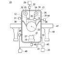
- Reference numeral 20 in FIG. 1 is a vapor deposition apparatus for producing the optical thin film of the present invention and the optical film of the present invention.
- the vapor deposition apparatus 20 has a vacuum chamber 21.
- Reference numeral 48 denotes a vacuum exhaust device, and reference numeral 47 denotes an exhaust pipe.
- a rotary shaft 33 arranged horizontally is provided inside the vacuum chamber 21, and the cylindrical main rotary drum 22 rotates on the rotary shaft 33 with the central axis thereof coinciding with the rotary shaft 33. It is attached to the shaft 33.
- a sorting plate 38 is provided in the vicinity of the main rotating drum 22, and the inside of the vacuum chamber 21 is divided into a preparation chamber 36 and a film forming chamber 37 by the main rotating drum 22 and the sorting plate 38.
- the preparation chamber 36 is a portion above the main rotating drum 22
- the film forming chamber 37 is a portion below the main rotating drum 22.
- a main motor (not shown) is disposed outside the vacuum chamber 21.
- the main rotating drum 22 rotates at the same rotational speed as the rotating shaft 33. It has become.
- the circumferential portion of the main rotating drum 22 (the circumferential portion means a side surface of the cylindrical main rotating drum 22) is arranged inside the preparation chamber 36 and the film forming chamber. 37 alternately passes through the inside.
- a feed shaft 24 and a take-up shaft 25 are provided inside the preparation chamber 36.
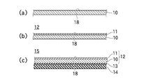
- Reference numeral 10 in FIG. 3A denotes a substrate to be vapor-deposited which is an object on which an optical thin film is formed by the vapor deposition apparatus 20.
- the substrate 10 to be deposited is a flexible film made of resin, and for example, a PET film can be used.
- a surface treatment device 26 is disposed at a position between the feed shaft 24 and the main rotating drum 22, and as shown in FIG.
- the raw fabric roll 34 is mounted on the feed shaft 24, the end of the deposition target substrate 10 is pulled out from the raw fabric roll 34, the direction of the deposition target substrate 10 is changed by contacting the auxiliary rotation shaft 39, and the surface
- the end of the drawn substrate 10 is moved from the preparation chamber 36 to the film formation chamber 37 and then returned to the preparation chamber 36.
- the film is stretched over the main rotating drum 22 and comes into contact with the circumferential portion of the main rotating drum 22.
- the end of the vapor deposition substrate 10 that has returned to the preparation chamber 36 is fixed to a take-up reel 35 attached to the take-up shaft 25.
- a winding motor is attached to the winding shaft 25, and a feeding motor is attached to the feeding shaft 24.
- the main motor, the take-up motor, and the feed motor are operated to rotate the take-up shaft 25, the main rotary drum 22, and the feed shaft 24, the deposition target substrate 10 is pulled out from the original fabric roll 34.
- the preparation chamber 36 is returned to the take-up reel 35.
- the film forming chamber 37 is provided with an evaporator 27 in which a metal material that generates steam is disposed.
- the metal material is indium metal (In) or tin metal (Sn).
- the evaporation device 27 is provided with a heating device 19.
- the heating device 19 When the heating device 19 is energized by a heating power supply 46, the heating device 19 operates to heat the metal material.
- Vacuum evacuation devices 31 and 48 are connected to the preparation chamber 36 and the film formation chamber 37, respectively.
- the metal material When the metal material is heated in the vacuum atmosphere, the metal material evaporates, and the vapor of the metal material is released from the discharge port 41 into the vacuum atmosphere of the film formation chamber 37.
- An oxygen gas introducing device 23 filled with oxygen gas is connected to the film forming chamber 37, and oxygen gas can be introduced into the film forming chamber 37 from a gas introduction hole 42 provided in the film forming chamber 37. Has been.
- a flow rate control device 43 is provided in the middle of a flow path (piping) of oxygen gas flowing from the oxygen gas introduction device 23 to the gas introduction port 42, and the oxygen gas introduction device is operated by operating the flow rate control device 43.
- the flow rate of oxygen gas introduced from 23 into the film forming chamber 37 can be controlled.
- a partial pressure measuring device 28 is provided in the film forming chamber 37, and the partial pressure value of oxygen gas in a vacuum atmosphere formed in the film forming chamber 37 is measured.
- Oxygen gas is introduced into the film forming chamber 37 while being evacuated, and the flow rate of the introduced oxygen gas is adjusted while maintaining the evacuation speed at a constant value and measuring the partial pressure value of the oxygen gas in the vacuum atmosphere. Since it can be changed, the vacuum atmosphere inside the film forming chamber 37 can contain oxygen gas having a desired partial pressure value.
- the inside of the film forming chamber 37 can be set to a desired oxygen gas partial pressure.
- the surface 18 of the deposition target substrate 10 faces the discharge port 41, while the back surface is in contact with the main rotating drum 22.
- the vapor of the metal material is released from the discharge port 41, the vapor reaches the facing part of the surface 18 of the substrate 10 to be deposited, and a part of the metal material is in a vacuum atmosphere.
- An optical thin film that is a thin film of a metal material containing the generated metal oxide that reacts with oxygen gas is formed on the surface 18 of the substrate 10 to be deposited.
- Reference numeral 11 in FIG. 3B denotes an optical thin film formed on the surface 18 of the substrate 10 to be deposited. If the traveling speed of the portion facing the discharge port 41 of the substrate 10 to be vapor-deposited and the vapor release rate (discharge amount / unit time) are constant values, the substrate 10 to be deposited has a lengthwise direction. Thus, the optical thin film 11 having a constant film thickness value is formed.
- the film thickness value of the optical thin film 11 to be formed can be changed by changing at least one of the traveling speed of the substrate 10 and the vapor release speed.
- the vapor deposition apparatus 20 is provided with a main controller 40 that controls the operation of each apparatus in the vapor deposition apparatus 20.
- the main controller 40 is connected to a heating power source 46, motors for rotating the shafts 24, 25, 33, a flow controller 43, a partial pressure measuring device 28, and vacuum evacuators 31, 48.
- a control signal can be input and output between the main control device 40 and each device connected to the main control device 40.
- the main control device 40 controls the flow rate control device 43, the flow rate of oxygen gas introduced into the film forming chamber 37 from the gas introduction port 42 is increased or decreased.
- the main control device 40 controls the heating power source 46, the heating power source 46
- the shafts 24, 25, and 33 can be rotated at a desired rotational speed.
- the main controller 40 can set values such as a partial pressure value of oxygen gas in a vacuum atmosphere and a film thickness value of the optical thin film 11 for forming the optical thin film 11.
- the partial pressure value of the oxygen gas measured by the partial pressure measuring device 28 is output to the main control device 40, and the main control device 40 sets the partial pressure value input from the partial pressure measuring device 28 as a reference value.
- the film formation chamber is changed.
- the partial pressure value of the oxygen gas contained in the 37 vacuum atmosphere is equal to the partial pressure value set as the reference value.
- optical thin film formation process Next, the optical thin film formation process which forms the optical thin film 11 using the said vapor deposition apparatus 20 is demonstrated.
- the traveling speed of the deposition target substrate 10 at the position facing the discharge port 41, and the discharge speed of the vapor discharged from the discharge port 41 corresponds to the input power to the heating device 19, the relationship between the rotational speed of the main rotating drum 22 and By controlling the input power to the heating device 19, the optical thin film 11 having a desired film thickness value can be formed on the deposition target substrate 10.
- the main controller 40 obtains the value of the rotational speed of the main rotating drum 22 and the value of the input power to the heating device 19 with respect to the film thickness value, and the main motor and the heating
- the optical thin film 11 having a set film thickness value can be formed on the deposition target substrate 10 by controlling the power supply 46.
- the evacuation devices 31 and 48 are activated by the main controller 40 in advance, and the preparation chamber 36 and the film formation chamber 37 are evacuated to form a vacuum atmosphere.
- a vacuum atmosphere containing oxygen gas is formed in the film forming chamber 37 by the main controller 40, and is maintained at the set partial pressure value and pulled out from the raw roll 34.
- the optical material contains an oxide of the metal material and is made of the metal material having a set film thickness value.
- the thin film 11 is formed, and the optical film 12 composed of the deposition target substrate 10 and the optical thin film 11 is wound on the take-up reel 35.
- the optical thin film 11 is formed in close contact with the substrate 10 to be deposited, but a thin film different from the optical thin film 11 may be formed on the substrate 10 to be deposited.
- any one of the partial pressure value of oxygen gas at the time of forming the optical thin film 11 and the film thickness value of the optical thin film 11 to be formed is different, the optical characteristics described later of the obtained optical thin film 11 are different.
- the pressure value and the film thickness value constitute a set of formation conditions for making optical characteristics different.
- Such a plurality of different formation conditions are prepared in advance, and in order to form the optical thin film 11 that is the first measurement object, first, one of the plurality of prepared formation conditions is first selected.
- the partial pressure value and the film thickness value included in the formation condition are set in the main controller 40, and the optical thin film forming process is performed with the set partial pressure value and the film thickness value.
- the optical thin film 11 that is the first object to be measured is formed under the following formation conditions.
- the optical thin film 11 is formed as the second object to be measured, which is different from the first formation condition under the second selected formation condition.
- the optical thin film 11 that is a plurality of measurement objects having at least different film thickness values or optical characteristics is formed under a plurality of formation conditions.
- the optical thin film 11 as each measurement object is taken out from the inside of the vacuum chamber 21.
- the optical thin film 11 may be formed under the formation condition on the surface of the substrate 10 to be vapor-deposited by the surface treatment process described later. Good.
- a color characteristic represented by a chromaticity value of at least one of a * and b * and an optical density value (OD value) is an optical characteristic.
- the optical properties of each optical thin film 11 formed in the measurement object forming step are measured using an optical density measuring device (Ihara Electronics Co., Ltd., product name Ihac-T5) and a spectrocolorimeter (Konica Minolta, product name).
- CM-5 (measurement wavelength 360 nm to 740 nm) is recorded in association with the partial pressure value on which the optical thin film 11 is formed and the film thickness value of the optical thin film 11.
- the measurement result obtained by measuring the film thickness value of the formed optical thin film 11 with the film thickness measurement device is assumed to be equal to the film thickness value set in the main control device 40. If the set film thickness value is significantly different, the film thickness value of the measurement result may be recorded in association with the optical characteristic and the partial pressure value.
- both the transmission a * and the transmission b * are measured, the value of the measurement result of a * and the value of the measurement result of b * are defined as chromaticity, and the value and chromaticity of the measurement result of optical density are optically measured.
- the characteristics are associated with the partial pressure value and the film thickness value, but either one of a * and b * is measured, and the value of the measurement result is defined as chromaticity, and the chromaticity and optical density are optically measured. It may be recorded in association with the partial pressure value and the film thickness value included in the characteristics.
- the optical characteristics are measured in the measurement process, and the partial pressure value, the film thickness value, and the optical characteristics are recorded in association with each other.
- ⁇ Analysis process> for each optical thin film 11, based on the associated partial pressure value, film thickness value, and optical characteristic, from the chromaticity value and optical density value included in the associated optical characteristic, a film is obtained.
- the partial pressure value can be obtained from the correspondence relationship in which the thickness value and the partial pressure value are obtained, or from the chromaticity value, the optical density value, and the film thickness value included in the associated optical characteristics. Find correspondence.
- the correspondence relationship may be, for example, an approximate function that can calculate the partial pressure value from the optical characteristic and the film thickness value, or, for example, record the partial pressure value, the film thickness value, and the optical characteristic as a database,
- the optical characteristics for which there is no data corresponding to the database may be a correspondence relationship in which the partial pressure value and the film thickness value are obtained by a complementing method.
- the correspondence relationship obtained in the analysis process is stored in the main controller 40.
- ⁇ Calculation process> In order to manufacture the desired optical film 12, first, when the hue and film thickness value of the optical thin film 11 to be formed are specified, the hue is converted into chromaticity and optical density included in the corresponding relationship. When the optical characteristics including the chromaticity and optical density obtained by the conversion and the specified film thickness value are input to the main controller 40, the main controller 40 obtains a partial pressure value from the stored correspondence. The specified film thickness value and the obtained partial pressure value are used as the forming conditions.
- the hue is specified and the film thickness value is not specified, the hue is converted into chromaticity and optical density, and the chromaticity and optical density are checked in correspondence, and the film thickness value and partial pressure value are compared. And ask.
- one set of film thickness values and partial pressure values is determined as a forming condition.
- the partial pressure value may be replaced with a flow rate value of oxygen gas to achieve the partial pressure value.
- optical thin film formation process optical film formation process>
- the main controller 40 is set with a partial pressure value or an oxygen flow rate value and a film thickness value included in the formation conditions determined in the calculation step, and the partial pressure value or oxygen flow rate set by the optical thin film formation step is set.
- an optical thin film 11 made of a metal with a set film thickness is formed on the vapor deposition substrate 10 to obtain an optical film 12.
- the optical characteristic of the correspondence obtained in the analysis step is a measured value of the optical thin film 11 formed on the surface of the deposition target substrate 10 subjected to the surface treatment in the surface treatment step described later
- the optical thin film formation step Then, the optical film 12 is manufactured by forming the optical thin film 11 on the surface of the evaporation target substrate 10 that has been surface-treated in the surface treatment step under the same conditions.
- the take-up reel 35 on which the optical film 12 manufactured in this way is taken out is taken out from the preparation chamber 36 into the atmosphere, cut into a desired shape, and attached to a plate glass or the like.
- Table 1 shows the measurement results of the optical characteristics of the optical thin film 11 made of metal In as a metal material
- Table 2 shows the measurement results of the optical characteristics of the optical thin film 11 made of metal Sn as a metal material.
- Tables 1 and 2 show the partial pressure value of oxygen gas, the transmission L * a * b * of the optical thin film 11 formed with the partial pressure value, the measured value of L * in the color system, the measured value of a * , b
- the measured value of * and the measured value of optical density (OD value) are described as optical characteristics.
- the optical thin film 11 having the same partial pressure value and the optical characteristics are distinguished from each other by attaching the same symbol of symbols A 1 to A 5 in Table 1 below. Also in Table 2 below, the same symbols out of the symbols B 1 to B 5 are given and distinguished.
- Symbols A 1 to A 5 have partial pressure values of less than 1.0 ⁇ 10 ⁇ 5 Pa, 5 ⁇ 10 ⁇ 5 Pa, 3 ⁇ 10 ⁇ 4 Pa, 2 ⁇ 10 ⁇ 3 Pa, 1 ⁇ 10 ⁇ 2 Pa
- the symbols B 1 to B 5 are less than 1.0 ⁇ 10 ⁇ 5 Pa, 1.2 ⁇ 10 ⁇ 4 Pa, 1.0 ⁇ 10 ⁇ 3 Pa, 4.1 ⁇ 10 ⁇ 3 Pa, This is a classification of 8.0 ⁇ 10 ⁇ 3 Pa.
- the “partial pressure value of oxygen gas (Pa)” is a value measured by a partial pressure measuring device 28 (trade name “Qulee” manufactured by ULVAC, Inc.).
- FIGS. 4 and 6 show the relationship between the measured value of the chromaticity b * of the L * a * b * color system and the optical density of the optical thin film 11 based on the measurement results of Tables 1 and 2, respectively.
- the horizontal axis indicates the value of b *
- the vertical axis indicates the value of optical density.
- the curves shown in FIGS. 4 and 6 are obtained by connecting the measured values of the same partial pressure values.
- the partial pressure values of the respective curves are represented by symbols A 1 to A 5 and symbols B 1 to B indicating the partial pressure values. 5 is described as a symbol for distinguishing the curves.
- the film thickness value increases, the optical density increases, and when the film thickness value decreases, the optical density also decreases. Therefore, in order to increase the value of b * , the film thickness value is decreased and the value of b * is decreased. For this, the film thickness value may be increased.
- the measured value of b * increases.
- the maximum value is obtained at the partial pressure value of the curve A 3 and the partial pressure value of the curve B 2 , and in a range larger than the partial pressure value, the measured value of b * decreases as the partial pressure value increases. Therefore, by changing the partial pressure value, it is possible to change the value of b * while maintaining the optical density at a constant value.
- the input electric power is constant, and the film thickness value of the optical thin film 11 to be formed is made different by changing the transport speed of the substrate 10 to be deposited.
- the partial pressure value is less than 1.0 ⁇ 10 ⁇ 5 Pa, both the input power and the conveyance speed are changed, whereas the partial pressure value is 1.0 ⁇ 10 ⁇ 5 Pa or more.
- the value of input power is made constant, the optical thin film 11 having a different film thickness value is formed by changing the conveyance speed.
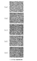
- 5 (a) to 5 (e) are electron micrographs of the optical thin film 11 having partial pressure values classified into symbols A 1 to A 5 , respectively, and particularly classified into symbols A 1 to A 5 in Table 1.
- 3 is an electron micrograph of the surface of the optical thin film 11 having an optical density of about 1.0 in the optical thin film 11.
- FIGS. 7A to 7E are electron micrographs of the optical thin film 11 having partial pressure values classified into symbols B 1 to B 5 , respectively, and particularly classified into symbols B 1 to B 5 in Table 2.
- 4 is an electron micrograph of the optical thin film 11 having an optical density of about 0.85 in the measurement result.
- the optical density increases even if the film thickness value of the optical thin film 11 is increased by decreasing the conveying speed.
- the reason is that, in the state where the oxygen partial pressure in the vacuum atmosphere is low, the vapor of the metal material easily moves on the surface of the substrate 10 to be deposited, and the particle size becomes large. In that case, it is presumed that the optical density was lowered because high-height particles were formed and the gaps between the particles were large (FIGS. 5A and 7A).
- the particle size is reduced. In that case, particles having a low height are formed, and the gap between the particles becomes small, so it is presumed that the value of the optical density has increased.
- the vapor deposition substrate 10 drawn from the raw roll 34 passes through the inside of the surface treatment apparatus 26, and then comes into contact with the main rotating drum 22 and travels in the film forming chamber 37. ing.
- a surface treatment gas introduction device 29 and a surface treatment power source 44 are connected to the surface treatment device 26.
- the surface treatment gas introduction device 29 and the surface treatment power supply 44 are connected to the main control device 40, and the flow rate is controlled by the flow rate control device 32 under the control of the main control device 40, while the surface treatment gas introduction device 29 supplies the surface.
- a surface treatment gas is introduced into the treatment device 26 so that electric power is supplied from the surface treatment power supply 44 to the surface treatment device 26.
- plasma of the surface treatment gas introduced from the surface treatment gas introduction device 29 is formed inside the surface treatment device 26 by the supplied power. Is done.
- the substrate to be deposited 10 passes through the inside of the surface treatment apparatus 26 in which the plasma of the surface treatment gas is formed, the surface of the substrate to be deposited 10 is exposed to the plasma and the surface is modified.
- the optical density is higher than when the plasma treatment is not performed. The value of increases.
- the surface treatment apparatus 26 is not operated, and the measured values in Tables 1 and 2 are the measurement results of the optical thin film 11 formed when the surface treatment apparatus 26 did not operate.
- optical characteristics of the optical thin film 11 subjected to the surface treatment and the optical characteristics of the optical thin film 11 when the surface treatment was not performed were measured.
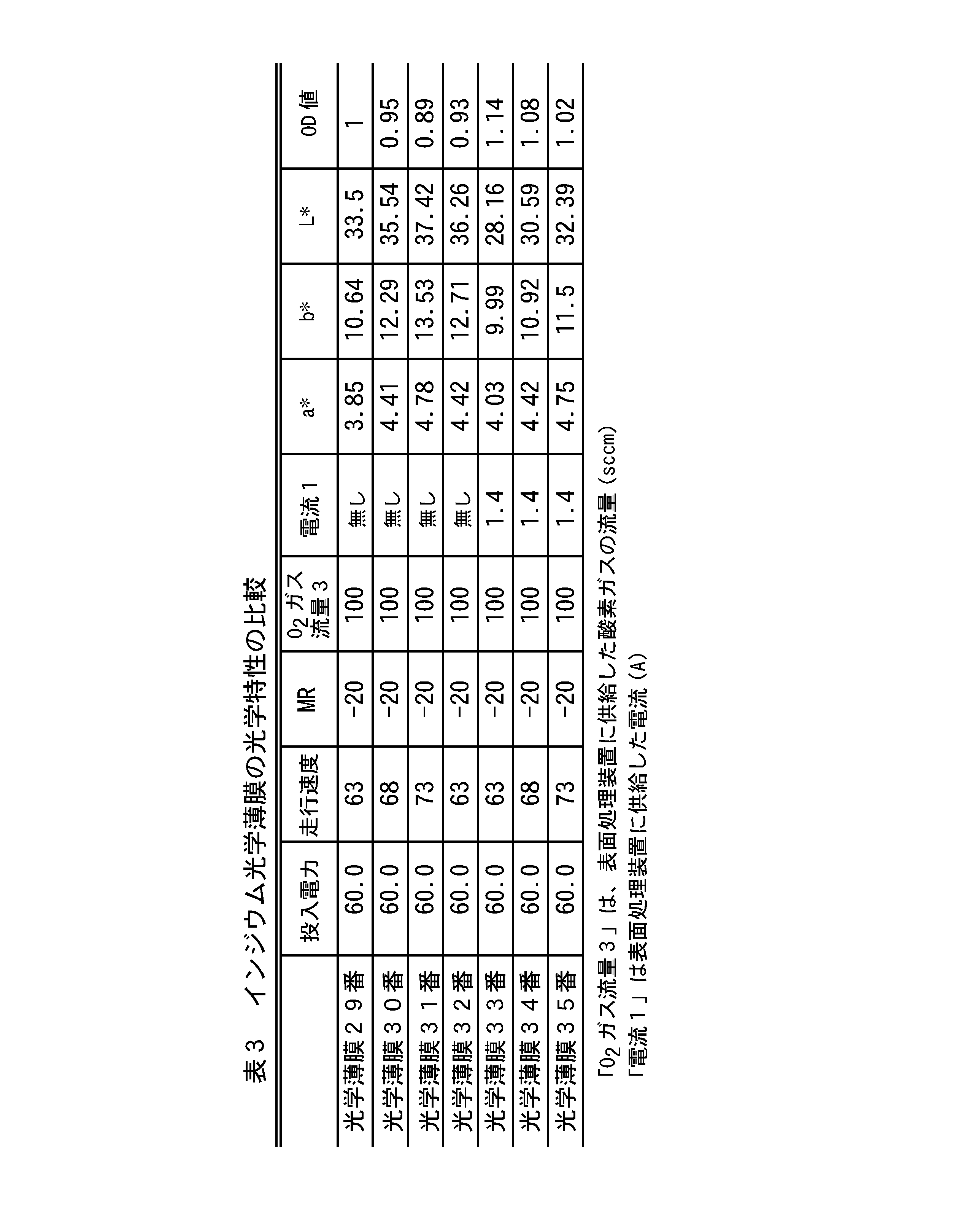
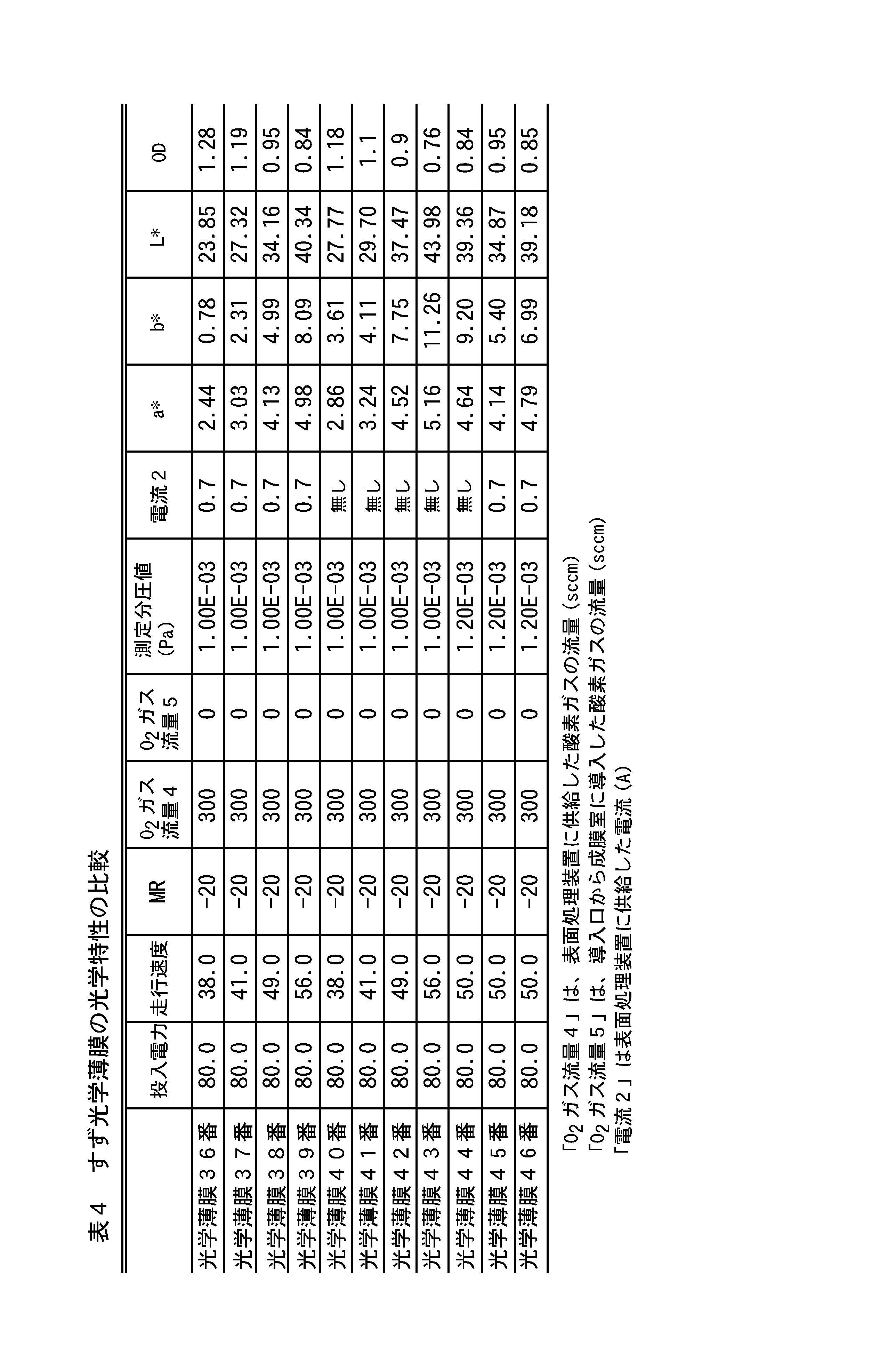
- the measurement results of the optical thin film 11 made of an indium thin film containing indium oxide are shown in Table 3 below, and the measurement results of the optical thin film 11 made of a tin thin film containing tin oxide are shown in Table 4 below.
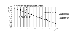
- Symbol C in FIG. 8 is a curve obtained from the measured values of the optical thin films Nos. 29 to 35 in Table 3.
- the measured values of the optical thin films No. 29 to No. 32 that were not subjected to the surface treatment and the surface treatment were performed. Further, the optical thin films Nos. 33 to 35 are located on or near the curve C thereof.
- FIGS. 9A and 9B are photomicrographs of the surface of the optical thin film No. 29 not subjected to surface treatment and the surface of the optical thin film No. 35 subjected to surface treatment, respectively
- FIG. , (D) are photomicrographs of the surface of the optical thin film No. 32 not subjected to the surface treatment and the surface of the optical thin film No. 33 subjected to the surface treatment, respectively. It can be seen that the gap between the particles is large when the surface treatment is not performed.
- the symbol D in FIG. 10 is a curve obtained from the measured values of the optical thin films 36 to 43 in Table 4, and the measured values of the optical thin films 36 to 43 are located in the vicinity of the same curve D. Therefore, it can be said that a constant relationship between the value of b * and the value of optical density is maintained regardless of the presence or absence of the surface treatment in the tin thin film containing tin oxide.
- the value of the optical density can be increased.
- FIGS. 11A and 11B are micrographs of the surface of the optical thin film No. 39 subjected to the surface treatment and the surface of the optical thin film No. 42 not subjected to the surface treatment
- FIG. (d) is a photomicrograph of the surface of the optical thin film No. 44 not subjected to surface treatment and the surface of the optical thin film No. 45 subjected to surface treatment, respectively.
- the gap between the particles is large.
- FIG. 3 (c) shows a window glass 15 in which the optical film 12 of the present invention is attached to a plate glass 14 with an adhesive layer 13.
- the resistance value of the optical thin film 11 of the optical film 12 is large.
- the film thickness value increases, the resistance value decreases, and when the film thickness value decreases, the resistance value increases.Therefore, the correspondence relationship between the resistance value, the film thickness value, the partial pressure value, and the optical characteristics is obtained in advance.
- the film thickness value, the optical characteristic, and the resistance value are set, and the optical thin film 11 having the desired optical characteristic and resistance value can be formed.
- the optical thin film 11 having desired optical characteristics, resistance values, and film thickness values can be formed by setting optical characteristics and resistance values.
- the optical density value increases when the surface treatment is performed. Therefore, the optical density value can be increased without reducing the resistance value by performing the surface treatment.
- the optical thin film 11 is formed on the surface of the vapor deposition substrate 10 made of a flexible resin film.
- the optical thin film 11 is formed on the surface of a plate-like glass or the surface of a plate-like resin. You can also
- the partial pressure value measured by the partial pressure measurement device 28 is controlled by the partial pressure measurement device 28 and the flow rate control device 43 so as to be equal to the set partial pressure value.
- both the evacuation speed of the evacuation device 48 that evacuates the film forming chamber 37 and the introduction amount of the flow rate control device 43 may be controlled.
- the flow control device 43 may be used.
- the total pressure value may also be measured, and the vacuum exhaust device 48 may be controlled so that the total pressure value falls within a predetermined range. In short, it is only necessary that the partial pressure value of the oxygen gas contained in the vacuum atmosphere can be controlled to a desired value.
- the L * a * b * color system is used, but other color systems such as an XYZ color system and an RGB color system can also be used.
Landscapes
- Chemical & Material Sciences (AREA)
- Chemical Kinetics & Catalysis (AREA)
- Engineering & Computer Science (AREA)
- Materials Engineering (AREA)
- Mechanical Engineering (AREA)
- Metallurgy (AREA)
- Organic Chemistry (AREA)
- Physics & Mathematics (AREA)
- General Physics & Mathematics (AREA)
- Optics & Photonics (AREA)
- Physical Vapour Deposition (AREA)
- Optical Filters (AREA)
Abstract
Description
しかしながら、太陽光には紫外線や赤外線が含まれており、近年ではその害が注目され、窓ガラスを太陽光が通過する際に、特定の波長の光を除去する技術が求められている。
また、本発明は、前記測定対象形成工程で形成された複数の前記光学薄膜の前記試験流量値と膜厚値と、測定された前記光学特性とから、前記試験流量値と前記膜厚値と前記光学特性との間の対応関係を求める解析工程と、形成する前記光学薄膜の、前記測定工程で測定された前記光学特性に含まれる前記光学濃度と色度とを前記対応関係に照合し、少なくとも形成する前記光学薄膜の算出流量値を求める算出工程と、を有し、前記算出工程で求めた前記算出流量値を前記設定流量値として設定し、前記光学薄膜工程で前記光学薄膜を形成する光学薄膜製造方法である。
また、本発明は、前記算出工程では、形成する前記光学薄膜の光学濃度と色度と膜厚値とを前記対応関係に照合し、形成する前記光学薄膜の前記算出流量値を求める光学薄膜製造方法である。
また、本発明は、前記算出工程では、形成する前記光学薄膜の光学濃度と色度とを前記対応関係に照合し、形成する前記光学薄膜の前記算出流量値と前記膜厚値とを求め、前記光学薄膜形成工程では前記算出工程で求めた前記膜厚値の前記光学薄膜を形成する光学薄膜製造方法である。
また、本発明は、前記光学薄膜形成工程では、前記算出流量値を前記設定流量値に設定することで、前記真空槽内の前記酸素ガスの分圧を予め設定された値にする光学薄膜製造方法である。
また、本発明は 前記光学薄膜を被蒸着基材の表面に形成する光学薄膜製造方法であって、前記被蒸着基材をプラズマに接触させ、前記被蒸着基材の表面処理を行う表面処理工程を有し、前記光学薄膜形成工程では、前記表面処理が行われた前記被蒸着基材の表面に前記光学薄膜を形成する光学薄膜製造方法である。
また、本発明は、真空槽内に形成された真空雰囲気に、設定された設定流量値で酸素ガスを供給し、金属In又は金属Snのいずれか一方から成り、蒸発源に配置された金属材料を加熱して蒸発させ、発生した前記金属材料の蒸気を前記真空雰囲気中に放出させ、前記蒸気から、前記金属材料の酸化物から成る光学薄膜を形成する光学薄膜形成工程を有する光学フィルム製造方法であって、異なる値の複数の試験流量値を前記設定流量値として設定し、前記光学薄膜形成工程によって複数の前記光学薄膜を形成する測定対象形成工程と、前記測定対象形成工程で形成された各前記光学薄膜の光学濃度または透過率の少なくとも一方を含む光学特性を測定する測定工程と、を有し、フィルム状の被蒸着基材上に前記光学薄膜を形成する光学フィルム製造方法である。
また、本発明は、前記測定対象形成工程で形成された複数の前記光学薄膜の前記試験流量値と膜厚値と、測定された前記光学特性とから、前記試験流量値と前記膜厚値と前記光学特性との間の対応関係を求める解析工程と、形成する前記光学薄膜の、前記測定工程で測定された前記光学特性に含まれる前記光学濃度と色度とを前記対応関係に照合し、少なくとも形成する前記光学薄膜の算出流量値を求める算出工程と、を有し、前記算出工程で求めた前記算出流量値を前記設定流量値として設定し、前記光学薄膜形成工程で前記光学薄膜を形成する光学フィルム製造方法である。
また、本発明は、前記算出工程では、形成する前記光学薄膜の光学濃度と色度と膜厚値とを前記対応関係に照合し、形成する前記光学薄膜の前記算出流量値を求める光学フィルム製造方法である。
また、本発明は、前記算出工程では、形成する前記光学薄膜の光学濃度と色度とを前記対応関係に照合し、形成する前記光学薄膜の前記算出流量値と前記膜厚値とを求め、前記光学薄膜形成工程では前記算出工程で求めた前記膜厚値の前記光学薄膜を形成する光学フィルム製造方法である。
また、本発明は、前記光学薄膜形成工程では、前記算出流量値を前記設定流量値に設定することで、前記真空槽内の前記酸素ガスの分圧を予め設定された値にする光学フィルム製造方法である。
また、本発明は、前記被蒸着基材をプラズマに接触させ、前記被蒸着基材の表面処理を行う表面処理工程を有し、前記光学薄膜形成工程では、前記表面処理が行われた前記被蒸着基材の表面に前記光学薄膜を形成する光学フィルム製造方法である。
本発明には、真空槽内に形成された真空雰囲気に、設定された設定分圧値で酸素ガスを含有させ、蒸発源に配置された金属材料を加熱して蒸発させ、発生した前記金属材料の蒸気を前記真空雰囲気中に放出させ、前記蒸気から、前記金属材料の酸化物を含有する前記金属材料の薄膜である光学薄膜を形成する光学薄膜形成工程を有する光学薄膜製造方法であって、異なる値の複数の試験分圧値を前記設定分圧値として設定し、前記光学薄膜形成工程によって複数の前記光学薄膜を形成する測定対象形成工程と、前記測定対象形成工程で形成された各前記光学薄膜の光学濃度または透過率の少なくとも一方を含む光学特性を測定する測定工程と、を有し、前記光学特性から前記設定分圧値を設定する光学薄膜製造方法も含まれる。
また、本発明には、前記測定対象形成工程で形成された複数の前記光学薄膜の前記試験分圧値と膜厚値と、測定された前記光学特性とから、前記試験分圧値と前記膜厚値と前記光学特性との間の対応関係を求める解析工程と、形成する前記光学薄膜の、前記測定工程で測定された前記光学特性に含まれる前記光学濃度と色度とを前記対応関係に照合し、少なくとも形成する前記光学薄膜の算出分圧値を求める算出工程と、を有し、前記算出工程で求めた前記算出分圧値を前記光学薄膜形成工程に前記設定分圧値として設定し、前記光学薄膜形成工程では、前記算出工程で求めた膜厚値の前記光学薄膜を形成する光学薄膜形成工程を有する上記光学薄膜製造方法も含まれる。
また、前記算出工程では、、形成する前記光学薄膜の光学濃度と色度と膜厚値とを前記対応関係に照合し、形成する前記光学薄膜の前記算出分圧値を求める上記光学薄膜製造方法も含本発明に含まれる。
また、本発明には、前記算出工程では、形成する前記光学薄膜の光学濃度と色度とを前記対応関係に照合し、形成する前記光学薄膜の前記算出分圧値と前記膜厚値とを求め、前記光学薄膜工程では前記算出工程で求めた前記膜厚値の前記光学薄膜を形成する上記光学薄膜製造方法も含まれる。
また、本発明には、前記光学薄膜形成工程では、前記算出分圧値を前記設定分圧値に設定することで、前記真空槽内に供給する前記酸素ガスを設定された設定流量値で供給する上記光学薄膜製造方法も含まれる。
また、本発明には、前記光学薄膜を被蒸着基材の表面に形成する光学薄膜製造方法であって、前記被蒸着基材をプラズマに接触させ、前記被蒸着基材の表面処理を行う表面処理工程を有し、前記光学薄膜形成工程では、前記表面処理が行われた前記被蒸着基材の表面に前記光学薄膜を形成する光学薄膜製造方法も含まれる。
また、本発明には、真空槽内に形成された真空雰囲気に、設定された設定分圧値で酸素ガスを含有させ、金属In又は金属Snのいずれか一方からなり、蒸発源に配置された金属材料を加熱して蒸発させ、発生した前記金属材料の蒸気を前記真空雰囲気中に放出させ、前記蒸気から、前記金属材料の酸化物から成る光学薄膜を形成する光学薄膜形成工程を有する光学フィルム製造方法であって、異なる値の複数の試験分圧値を前記設定分圧値として設定し、前記光学薄膜形成工程によって複数の前記光学薄膜を形成する測定対象形成工程と、前記測定対象形成工程で形成された各前記光学薄膜の光学濃度又は透過率の少なくとも一方を含む光学特性を測定する測定工程と、を有し、フィルム状の被蒸着基材上に前記光学薄膜を形成する光学フィルム製造方法も含まれる。
また、本発明には、前記測定対象形成工程で形成された複数の前記光学薄膜の前記試験分圧値と膜厚値と、測定された前記光学特性とから、前記試験分圧値と前記膜厚値と前記光学特性との間の対応関係を求める解析工程と、形成する前記光学薄膜の、前記測定工程で測定された前記光学特性に含まれる前記光学濃度と色度とを前記対応関係に照合し、少なくとも形成する前記光学薄膜の算出分圧値を求める算出工程と、を有し、前記算出工程で求めた前記算出分圧値を前記設定分圧値として設定し、前記光学薄膜形成工程で前記光学薄膜を形成する光学フィルム製造方法も含まれる。
また、本発明には、前記算出工程では、形成する前記光学薄膜の光学濃度と色度と膜厚値とを前記対応関係に照合し、形成する前記光学薄膜の前記算出分圧値を求める光学フィルム製造方法も含まれる。
また、前記算出工程では、形成する前記光学薄膜の光学濃度と色度と膜厚値とを前記対応関係に照合し、形成する前記光学薄膜の前記算出分圧値と前記膜厚値とを求め、前記光学薄膜形成工程では前記算出工程で求めた前記膜厚値の前記光学薄膜を形成する上記光学フィルム製造方法も本発明に含まれる。
また、本発明には、前記光学薄膜形成工程では、前記算出分圧値を前記設定分圧値に設定することで、前記真空槽内に供給する前記酸素ガスを設定された設定流量値で供給する上記光学フィルム製造方法も含まれる。
また、本発明には、前記被蒸着基材をプラズマに接触させ、前記被蒸着基材の表面処理を行う表面処理工程を有する光学フィルム製造方法であって、前記光学薄膜形成工程では、前記表面処理が行われた前記被蒸着基材の表面に前記光学薄膜を形成する光学フィルム製造方法も含まれる。
目で感じる色は、明るさと色の性質とによって決まるが、明るさを無視した色の性質は色度と呼ばれており、色度を表わすためには、複数の表色系が用いられており、各表色系では、明るさと色度の表現方法が異なっている。
光学濃度と色度とを色特性と呼ぶと、光学薄膜の色特性を含む特性を、光学特性と呼ぶものとする。
酸素ガスの流量もしくは酸素の分圧値を制御することで、膜厚値を変更せずに、光学濃度の値を変更することができる。
またプラズマ処理を制御することで、光学濃度の値を変更せずに、膜厚値を変更することが出来る。
また酸素の流量もしくは分圧値、およびプラズマ処理を同時に制御することで光学濃度と膜厚値を任意の値に変更することが出来る。
図1の符号20は、本発明の光学薄膜と本発明の光学フィルムを製造する蒸着装置である。
この蒸着装置20は真空槽21を有している。符号48は真空排気装置、符号47は排気配管である。
準備室36の内部には、送り出し軸24と、巻き取り軸25とが設けられている。
巻き取り軸25には、巻き取り用モータが取り付けられ、送り出し軸24には送り出し用モータが取り付けられている。主モータと巻き取り用モータと送り出し用モータとを動作させ、巻き取り軸25と、主回転ドラム22と、送り出し軸24とを回転させると、原反ロール34から被蒸着基材10が引き出され、準備室36から成膜室37に移動した後、準備室36に戻って巻き取りリール35に巻き取られる。
成膜室37には、蒸気を生成する金属材料が配置された蒸発装置27が設けられている。金属材料は、インジウム金属(In)、又は、すず金属(Sn)である。
準備室36と成膜室37とには、それぞれ真空排気装置31,48が接続されている。
成膜室37には、分圧測定装置28が設けられており、成膜室37内に形成された真空雰囲気中の酸素ガスの分圧値が測定される。
被蒸着基材10の放出口41と対面する部分の走行速度と、蒸気の放出速度(放出量/単位時間)とが一定値であれば、被蒸着基材10には、長さ方向に亘って一定の膜厚値の光学薄膜11が形成される。
次に、上記蒸着装置20を用いて光学薄膜11を形成する光学薄膜形成工程について説明する。
測定対象物を形成する測定対象形成工程について説明する。
このように複数の形成条件で、少なくとも膜厚値又は光学特性が異なる複数の測定対象物である光学薄膜11を形成する。各測定対象物である光学薄膜11は真空槽21の内部から取り出しておく。
各形成条件で測定対象物である光学薄膜11を形成する際に、後述する表面処理工程により、被蒸着基材10のプラズマで処理された表面に、形成条件で光学薄膜11を形成させてもよい。
次に、測定工程による光学特性の測定を説明する。
このように、測定対象形成工程で得られた各光学薄膜11には、測定工程で光学特性が測定され、分圧値と膜厚値と光学特性とが対応付けられて記録される。
解析工程では、各光学薄膜11毎に、対応付けられた分圧値と膜厚値と光学特性に基づき、対応付けられた光学特性に含まれる色度の値と光学濃度の値とから、膜厚値と分圧値とが求められる対応関係か、又は、対応付けられた光学特性に含まれる色度の値と光学濃度の値と、膜厚値とから、分圧値を求めることができる対応関係とを求める。
解析工程で求められた対応関係は、主制御装置40に記憶される。
所望の光学フィルム12を製造するために、先ず、形成すべき光学薄膜11の色合いと膜厚値とが特定された場合は、色合いを、対応関係に含まれる色度と光学濃度とに変換し、変換によって得られた色度と光学濃度とを含む光学特性と特定された膜厚値とを主制御装置40に入力すると、主制御装置40は、記憶する対応関係から、分圧値を求める、特定された膜厚値と求めた分圧値とを形成条件にする。
主制御装置40には、算出工程で決定された形成条件に含まれる分圧値または酸素流量値と膜厚値が設定されており、光学薄膜形成工程により、設定された分圧値または酸素流量値で酸素ガスを含有する真空雰囲気中で、設定された膜厚の金属から成る光学薄膜11が被蒸着基材10上に形成され、光学フィルム12が得られる。
次に、光学特性を測定した結果について説明する。
表1,2中、「酸素ガスの分圧値(Pa)」の値は、分圧測定装置28((株)アルバック社製、商品名「Qulee」)で測定した値である。


膜厚値が増加すると光学濃度は増加し、膜厚値が減少すると光学濃度も減少するから、b*の値を増加させるためには膜厚値を減少させ、b*の値を減少させるためには膜厚値を増加させればよい。
表2では、分圧値が1.0×10⁻⁵Pa未満のときに、投入電力と搬送速度の両方が変化されているのに対し、分圧値が1.0×10⁻⁵Pa以上の時は、表1と同様に、投入電力の値が一定にされ、搬送速度が異なる値にされて膜厚値が異なる光学薄膜11が形成されている。
蒸着装置20では、原反ロール34から引き出された被蒸着基材10は、表面処理装置26の内部を通過した後、主回転ドラム22と接触して成膜室37内を走行するようになっている。
表面処理ガスのプラズマが形成された表面処理装置26の内部を被蒸着基材10が通過すると、被蒸着基材10の表面がプラズマに曝され、表面が改質する。
表面処理を行わない場合には粒子間の隙間が大きくなっている。
図3(c)は、本発明の光学フィルム12を、接着剤層13によって、板ガラス14に貼付した窓ガラス15を示している。光学フィルム12が貼付された窓ガラス15では、光学フィルム12の導電性が高いと、電波が窓ガラス15を透過できなくなり、無線通信等に不都合が生じる。従って、光学フィルム12の光学薄膜11の抵抗値は大きい方が望ましい。
酸素ガスの分圧値が減少すると抵抗値は減少し、分圧値が増加すると抵抗値も増加する。
以上は、柔軟性を有する樹脂フィルムから成る被蒸着基材10の表面に、光学薄膜11を形成したが、光学薄膜11は、板状のガラスの表面や、板状の樹脂の表面に形成することもできる。
要するに、真空雰囲気中に含有される酸素ガスの分圧値を所望の値に制御することができればよい。
21……真空槽
36……準備室
37……成膜室
40……主制御装置
Claims (12)
- 真空槽内に形成された真空雰囲気に、設定された設定流量値で酸素ガスを供給し、蒸発源に配置された金属材料を加熱して蒸発させ、発生した前記金属材料の蒸気を前記真空雰囲気中に放出させ、前記蒸気から、前記金属材料の酸化物を含有する前記金属材料の薄膜である光学薄膜を形成する光学薄膜形成工程を有する光学薄膜製造方法であって、
異なる値の複数の試験流量値を前記設定流量値として設定し、前記光学薄膜形成工程によって複数の前記光学薄膜を形成する測定対象形成工程と、
前記測定対象形成工程で形成された各前記光学薄膜の光学濃度または透過率のうち少なくとも一方を含む光学特性を測定する測定工程と、
を有し、前記光学特性から前記設定流量値を設定する光学薄膜製造方法。 - 前記測定対象形成工程で形成された複数の前記光学薄膜の前記試験流量値と膜厚値と、測定された前記光学特性とから、前記試験流量値と前記膜厚値と前記光学特性との間の対応関係を求める解析工程と、
形成する前記光学薄膜の、前記測定工程で測定された前記光学特性に含まれる前記光学濃度と色度とを前記対応関係に照合し、少なくとも形成する前記光学薄膜の算出流量値を求める算出工程と、
を有し、
前記算出工程で求めた前記算出流量値を前記設定流量値として設定し、前記光学薄膜工程で前記光学薄膜を形成する請求項1記載の光学薄膜製造方法。 - 前記算出工程では、形成する前記光学薄膜の光学濃度と色度と膜厚値とを前記対応関係に照合し、形成する前記光学薄膜の前記算出流量値を求める請求項2記載の光学薄膜製造方法。
- 前記算出工程では、形成する前記光学薄膜の光学濃度と色度とを前記対応関係に照合し、形成する前記光学薄膜の前記算出流量値と前記膜厚値とを求め、前記光学薄膜形成工程では前記算出工程で求めた前記膜厚値の前記光学薄膜を形成する請求項2記載の光学薄膜製造方法。
- 前記光学薄膜形成工程では、前記算出流量値を前記設定流量値に設定することで、前記真空槽内の前記酸素ガスの分圧を予め設定された値にする請求項1記載の光学薄膜製造方法。
- 前記光学薄膜を被蒸着基材の表面に形成する請求項1記載の光学薄膜製造方法であって、
前記被蒸着基材をプラズマに接触させ、前記被蒸着基材の表面処理を行う表面処理工程を有し、
前記光学薄膜形成工程では、前記表面処理が行われた前記被蒸着基材の表面に前記光学薄膜を形成する光学薄膜製造方法。 - 真空槽内に形成された真空雰囲気に、設定された設定流量値で酸素ガスを供給し、金属In又は金属Snのいずれか一方から成り、蒸発源に配置された金属材料を加熱して蒸発させ、発生した前記金属材料の蒸気を前記真空雰囲気中に放出させ、前記蒸気から、前記金属材料の酸化物から成る光学薄膜を形成する光学薄膜形成工程を有する光学フィルム製造方法であって、
異なる値の複数の試験流量値を前記設定流量値として設定し、前記光学薄膜形成工程によって複数の前記光学薄膜を形成する測定対象形成工程と、
前記測定対象形成工程で形成された各前記光学薄膜の光学濃度または透過率の少なくとも一方を含む光学特性を測定する測定工程と、
を有し、
フィルム状の被蒸着基材上に前記光学薄膜を形成する光学フィルム製造方法。 - 前記測定対象形成工程で形成された複数の前記光学薄膜の前記試験流量値と膜厚値と、測定された前記光学特性とから、前記試験流量値と前記膜厚値と前記光学特性との間の対応関係を求める解析工程と、
形成する前記光学薄膜の、前記測定工程で測定された前記光学特性に含まれる前記光学濃度と色度とを前記対応関係に照合し、少なくとも形成する前記光学薄膜の算出流量値を求める算出工程と、を有し、
前記算出工程で求めた前記算出流量値を前記設定流量値として設定し、前記光学薄膜形成工程で前記光学薄膜を形成する請求項7記載の光学フィルム製造方法。 - 前記算出工程では、形成する前記光学薄膜の光学濃度と色度と膜厚値とを前記対応関係に照合し、形成する前記光学薄膜の前記算出流量値を求める請求項8記載の光学フィルム製造方法。
- 前記算出工程では、形成する前記光学薄膜の光学濃度と色度とを前記対応関係に照合し、形成する前記光学薄膜の前記算出流量値と前記膜厚値とを求め、前記光学薄膜形成工程では前記算出工程で求めた前記膜厚値の前記光学薄膜を形成する請求項8記載の光学フィルム製造方法。
- 前記光学薄膜形成工程では、前記算出流量値を前記設定流量値に設定することで、前記真空槽内の前記酸素ガスの分圧を予め設定された値にする請求項8記載の光学フィルム製造方法。
- 前記被蒸着基材をプラズマに接触させ、前記被蒸着基材の表面処理を行う表面処理工程を有する請求項7記載の光学フィルム製造方法であって、
前記光学薄膜形成工程では、前記表面処理が行われた前記被蒸着基材の表面に前記光学薄膜を形成する光学フィルム製造方法。
Priority Applications (3)
| Application Number | Priority Date | Filing Date | Title |
|---|---|---|---|
| JP2017520818A JP6577026B2 (ja) | 2015-05-27 | 2016-05-27 | 光学薄膜製造方法、光学フィルム製造方法 |
| CN201680030646.1A CN107614738B (zh) | 2015-05-27 | 2016-05-27 | 光学薄膜制造方法、光学膜片制造方法 |
| KR1020177034031A KR20170141753A (ko) | 2015-05-27 | 2016-05-27 | 광학 박막 제조 방법, 광학 필름 제조 방법 |
Applications Claiming Priority (2)
| Application Number | Priority Date | Filing Date | Title |
|---|---|---|---|
| JP2015107323 | 2015-05-27 | ||
| JP2015-107323 | 2015-05-27 |
Publications (1)
| Publication Number | Publication Date |
|---|---|
| WO2016190429A1 true WO2016190429A1 (ja) | 2016-12-01 |
Family
ID=57393514
Family Applications (1)
| Application Number | Title | Priority Date | Filing Date |
|---|---|---|---|
| PCT/JP2016/065790 Ceased WO2016190429A1 (ja) | 2015-05-27 | 2016-05-27 | 光学薄膜製造方法、光学フィルム製造方法 |
Country Status (4)
| Country | Link |
|---|---|
| JP (1) | JP6577026B2 (ja) |
| KR (1) | KR20170141753A (ja) |
| CN (1) | CN107614738B (ja) |
| WO (1) | WO2016190429A1 (ja) |
Families Citing this family (1)
| Publication number | Priority date | Publication date | Assignee | Title |
|---|---|---|---|---|
| KR102183063B1 (ko) * | 2019-01-31 | 2020-11-25 | 에스케이씨하이테크앤마케팅(주) | 그라데이션 필름 및 이의 제조방법 |
Citations (6)
| Publication number | Priority date | Publication date | Assignee | Title |
|---|---|---|---|---|
| JPS5137957A (ja) * | 1974-09-27 | 1976-03-30 | Fuji Photo Film Co Ltd | |
| JPS6082660A (ja) * | 1983-10-08 | 1985-05-10 | Konishiroku Photo Ind Co Ltd | 酸化物層の形成装置 |
| JPS61256943A (ja) * | 1985-05-10 | 1986-11-14 | Toyota Motor Corp | 有色透明導電膜の形成方法 |
| JPS6213567A (ja) * | 1985-07-09 | 1987-01-22 | Citizen Watch Co Ltd | 装飾部品の製造方法 |
| JPH06212403A (ja) * | 1993-01-18 | 1994-08-02 | Hitachi Ltd | 酸化In−Sn系透明導電膜の製造方法 |
| JPH1148387A (ja) * | 1997-08-08 | 1999-02-23 | Toppan Printing Co Ltd | 透明導電膜 |
Family Cites Families (1)
| Publication number | Priority date | Publication date | Assignee | Title |
|---|---|---|---|---|
| JP2001107232A (ja) * | 1999-10-04 | 2001-04-17 | Nikon Corp | 化合物薄膜形成方法及び光学薄膜及び光学素子 |
-
2016
- 2016-05-27 CN CN201680030646.1A patent/CN107614738B/zh active Active
- 2016-05-27 KR KR1020177034031A patent/KR20170141753A/ko not_active Ceased
- 2016-05-27 WO PCT/JP2016/065790 patent/WO2016190429A1/ja not_active Ceased
- 2016-05-27 JP JP2017520818A patent/JP6577026B2/ja active Active
Patent Citations (6)
| Publication number | Priority date | Publication date | Assignee | Title |
|---|---|---|---|---|
| JPS5137957A (ja) * | 1974-09-27 | 1976-03-30 | Fuji Photo Film Co Ltd | |
| JPS6082660A (ja) * | 1983-10-08 | 1985-05-10 | Konishiroku Photo Ind Co Ltd | 酸化物層の形成装置 |
| JPS61256943A (ja) * | 1985-05-10 | 1986-11-14 | Toyota Motor Corp | 有色透明導電膜の形成方法 |
| JPS6213567A (ja) * | 1985-07-09 | 1987-01-22 | Citizen Watch Co Ltd | 装飾部品の製造方法 |
| JPH06212403A (ja) * | 1993-01-18 | 1994-08-02 | Hitachi Ltd | 酸化In−Sn系透明導電膜の製造方法 |
| JPH1148387A (ja) * | 1997-08-08 | 1999-02-23 | Toppan Printing Co Ltd | 透明導電膜 |
Also Published As
| Publication number | Publication date |
|---|---|
| JP6577026B2 (ja) | 2019-09-18 |
| CN107614738A (zh) | 2018-01-19 |
| KR20170141753A (ko) | 2017-12-26 |
| JPWO2016190429A1 (ja) | 2018-02-22 |
| CN107614738B (zh) | 2019-10-18 |
Similar Documents
| Publication | Publication Date | Title |
|---|---|---|
| JP5081712B2 (ja) | 成膜装置 | |
| TWI567755B (zh) | Method for manufacturing transparent conductive film | |
| CN104023971B (zh) | 阻气膜和阻气膜的制造方法 | |
| CN1525912A (zh) | 铟锡氧化物的透明导电层状镀层 | |
| CN103562431B (zh) | 用于控制锂均匀度的改善的方法 | |
| CN103782201A (zh) | 用于制造在触控面板中使用的透明主体的方法和系统 | |
| JP6617607B2 (ja) | 成膜方法及びこれを用いた積層体基板の製造方法 | |
| JP7485107B2 (ja) | ガスバリアフィルムの製造方法 | |
| TW201708575A (zh) | 膜沉積設備和膜沉積方法 | |
| CN102312208B (zh) | 一种在树脂基片使用磁控溅射制备ito膜的方法 | |
| JP6577026B2 (ja) | 光学薄膜製造方法、光学フィルム製造方法 | |
| JP4580636B2 (ja) | 成膜装置および成膜方法 | |
| CN107839328A (zh) | 镀铝膜、微波复合膜及其制备方法 | |
| Nishikawa et al. | Growth of nanostructured VO2 via controlling oxidation of V thin films: morphology and phase transition properties | |
| US10752985B2 (en) | Laminate film and electrode substrate film, and method of manufacturing the same | |
| RU2564650C1 (ru) | Способ нанесения электропроводящего покрытия для электрообогреваемого элемента органического остекления | |
| Zulkifli et al. | Fabrication of transparent and flexible carbon‐doped ZnO field emission display on plastic substrate | |
| BE1029160B1 (nl) | Depositie van niet-stoichiometrische metaalverbindingen | |
| US20180265961A1 (en) | Reactive sputtering apparatus and reactive sputtering method | |
| TW201630720A (zh) | 積層體薄膜與電極基板薄膜及彼等之製造方法 | |
| WO2019031263A1 (ja) | ガスバリア性積層体 | |
| JP2009270133A (ja) | 機能性フィルム製造方法および機能性フィルム製造装置 | |
| JP5104273B2 (ja) | イオンプレーティング用蒸発源材料の原料粉末、イオンプレーティング用蒸発源材料及びその製造方法、ガスバリア性シート及びその製造方法 | |
| JP2009143759A (ja) | イオンプレーティング用蒸発源材料の原料粉末、イオンプレーティング用蒸発源材料及びその製造方法、ガスバリア性シート及びその製造方法 | |
| Chen et al. | Y2O3: Eu3+ luminescent thin film deposited on quartz fiber by electron beam evaporation technology |
Legal Events
| Date | Code | Title | Description |
|---|---|---|---|
| 121 | Ep: the epo has been informed by wipo that ep was designated in this application |
Ref document number: 16800133 Country of ref document: EP Kind code of ref document: A1 |
|
| ENP | Entry into the national phase |
Ref document number: 2017520818 Country of ref document: JP Kind code of ref document: A |
|
| ENP | Entry into the national phase |
Ref document number: 20177034031 Country of ref document: KR Kind code of ref document: A |
|
| NENP | Non-entry into the national phase |
Ref country code: DE |
|
| 122 | Ep: pct application non-entry in european phase |
Ref document number: 16800133 Country of ref document: EP Kind code of ref document: A1 |