WO2016190309A1 - 有機電子デバイス及び有機電子デバイス用基板 - Google Patents
有機電子デバイス及び有機電子デバイス用基板 Download PDFInfo
- Publication number
- WO2016190309A1 WO2016190309A1 PCT/JP2016/065321 JP2016065321W WO2016190309A1 WO 2016190309 A1 WO2016190309 A1 WO 2016190309A1 JP 2016065321 W JP2016065321 W JP 2016065321W WO 2016190309 A1 WO2016190309 A1 WO 2016190309A1
- Authority
- WO
- WIPO (PCT)
- Prior art keywords
- organic electronic
- electronic device
- substrate
- insulating layer
- organic
- Prior art date
- Legal status (The legal status is an assumption and is not a legal conclusion. Google has not performed a legal analysis and makes no representation as to the accuracy of the status listed.)
- Ceased
Links
Images

Classifications
-
- H—ELECTRICITY
- H10—SEMICONDUCTOR DEVICES; ELECTRIC SOLID-STATE DEVICES NOT OTHERWISE PROVIDED FOR
- H10K—ORGANIC ELECTRIC SOLID-STATE DEVICES
- H10K77/00—Constructional details of devices covered by this subclass and not covered by groups H10K10/80, H10K30/80, H10K50/80 or H10K59/80
- H10K77/10—Substrates, e.g. flexible substrates
-
- F—MECHANICAL ENGINEERING; LIGHTING; HEATING; WEAPONS; BLASTING
- F21—LIGHTING
- F21S—NON-PORTABLE LIGHTING DEVICES; SYSTEMS THEREOF; VEHICLE LIGHTING DEVICES SPECIALLY ADAPTED FOR VEHICLE EXTERIORS
- F21S2/00—Systems of lighting devices, not provided for in main groups F21S4/00 - F21S10/00 or F21S19/00, e.g. of modular construction
-
- H—ELECTRICITY
- H10—SEMICONDUCTOR DEVICES; ELECTRIC SOLID-STATE DEVICES NOT OTHERWISE PROVIDED FOR
- H10K—ORGANIC ELECTRIC SOLID-STATE DEVICES
- H10K30/00—Organic devices sensitive to infrared radiation, light, electromagnetic radiation of shorter wavelength or corpuscular radiation
- H10K30/80—Constructional details
-
- H—ELECTRICITY
- H10—SEMICONDUCTOR DEVICES; ELECTRIC SOLID-STATE DEVICES NOT OTHERWISE PROVIDED FOR
- H10K—ORGANIC ELECTRIC SOLID-STATE DEVICES
- H10K50/00—Organic light-emitting devices
-
- H—ELECTRICITY
- H10—SEMICONDUCTOR DEVICES; ELECTRIC SOLID-STATE DEVICES NOT OTHERWISE PROVIDED FOR
- H10K—ORGANIC ELECTRIC SOLID-STATE DEVICES
- H10K50/00—Organic light-emitting devices
- H10K50/80—Constructional details
- H10K50/84—Passivation; Containers; Encapsulations
- H10K50/844—Encapsulations
-
- H—ELECTRICITY
- H10—SEMICONDUCTOR DEVICES; ELECTRIC SOLID-STATE DEVICES NOT OTHERWISE PROVIDED FOR
- H10K—ORGANIC ELECTRIC SOLID-STATE DEVICES
- H10K77/00—Constructional details of devices covered by this subclass and not covered by groups H10K10/80, H10K30/80, H10K50/80 or H10K59/80
- H10K77/10—Substrates, e.g. flexible substrates
- H10K77/111—Flexible substrates
-
- F—MECHANICAL ENGINEERING; LIGHTING; HEATING; WEAPONS; BLASTING
- F21—LIGHTING
- F21Y—INDEXING SCHEME ASSOCIATED WITH SUBCLASSES F21K, F21L, F21S and F21V, RELATING TO THE FORM OR THE KIND OF THE LIGHT SOURCES OR OF THE COLOUR OF THE LIGHT EMITTED
- F21Y2115/00—Light-generating elements of semiconductor light sources
- F21Y2115/10—Light-emitting diodes [LED]
- F21Y2115/15—Organic light-emitting diodes [OLED]
-
- H—ELECTRICITY
- H10—SEMICONDUCTOR DEVICES; ELECTRIC SOLID-STATE DEVICES NOT OTHERWISE PROVIDED FOR
- H10K—ORGANIC ELECTRIC SOLID-STATE DEVICES
- H10K30/00—Organic devices sensitive to infrared radiation, light, electromagnetic radiation of shorter wavelength or corpuscular radiation
- H10K30/50—Photovoltaic [PV] devices
-
- H—ELECTRICITY
- H10—SEMICONDUCTOR DEVICES; ELECTRIC SOLID-STATE DEVICES NOT OTHERWISE PROVIDED FOR
- H10K—ORGANIC ELECTRIC SOLID-STATE DEVICES
- H10K50/00—Organic light-emitting devices
- H10K50/10—OLEDs or polymer light-emitting diodes [PLED]
-
- Y—GENERAL TAGGING OF NEW TECHNOLOGICAL DEVELOPMENTS; GENERAL TAGGING OF CROSS-SECTIONAL TECHNOLOGIES SPANNING OVER SEVERAL SECTIONS OF THE IPC; TECHNICAL SUBJECTS COVERED BY FORMER USPC CROSS-REFERENCE ART COLLECTIONS [XRACs] AND DIGESTS
- Y02—TECHNOLOGIES OR APPLICATIONS FOR MITIGATION OR ADAPTATION AGAINST CLIMATE CHANGE
- Y02E—REDUCTION OF GREENHOUSE GAS [GHG] EMISSIONS, RELATED TO ENERGY GENERATION, TRANSMISSION OR DISTRIBUTION
- Y02E10/00—Energy generation through renewable energy sources
- Y02E10/50—Photovoltaic [PV] energy
- Y02E10/549—Organic PV cells
-
- Y—GENERAL TAGGING OF NEW TECHNOLOGICAL DEVELOPMENTS; GENERAL TAGGING OF CROSS-SECTIONAL TECHNOLOGIES SPANNING OVER SEVERAL SECTIONS OF THE IPC; TECHNICAL SUBJECTS COVERED BY FORMER USPC CROSS-REFERENCE ART COLLECTIONS [XRACs] AND DIGESTS
- Y02—TECHNOLOGIES OR APPLICATIONS FOR MITIGATION OR ADAPTATION AGAINST CLIMATE CHANGE
- Y02P—CLIMATE CHANGE MITIGATION TECHNOLOGIES IN THE PRODUCTION OR PROCESSING OF GOODS
- Y02P70/00—Climate change mitigation technologies in the production process for final industrial or consumer products
- Y02P70/50—Manufacturing or production processes characterised by the final manufactured product
Definitions
- the present invention relates to an organic electronic device and a substrate for an organic electronic device.
- Organic electronic devices using organic semiconductors are flexible and thin, and are energy-saving, so they are expected to be applied to organic EL (electroluminescence) lighting and solar cells.
- the organic EL illumination requires a light emitting layer containing at least an organic semiconductor, and further includes a charge injection layer, an electrification transport layer, and the like in order to increase luminous efficiency.
- the solar cell includes a potential donor, an electron acceptor, and the like.
- the organic semiconductor since the organic semiconductor has a low charge mobility, it is often used in the form of an extremely thin film and is generally formed in a layer having a thickness of several tens of nanometers to several micrometers. Therefore, if the substrate (underlying material) on which the organic semiconductor is laminated has irregularities, it causes a short circuit of the device and decreases the manufacturing yield.
- an organic EL element has been proposed in which a resin coating film having a film thickness of 0.1 ⁇ m to several tens of ⁇ m is coated on a polished glass substrate in order to flatten abnormal projections on the substrate (Japanese Patent Laid-Open No. 2000) -21563).
- Japanese Patent Laid-Open No. 2000 Japanese Patent Laid-Open No. 2000
- -21563 Japanese Patent Laid-Open No. 2000
- an organic EL element having a metal plate or metal foil as a base material and an insulating layer having an organic resin film thickness of 1 to 40 ⁇ m, surface roughness Ra ⁇ 0.5 ⁇ m, and Rmax ⁇ 1.5 ⁇ m formed on the base material surface Insulating substrates have been proposed (see Japanese Patent Application Laid-Open No. 2002-25763).
- the present invention has been made based on the above-described circumstances, and an object thereof is to provide an organic electronic device and a substrate for an organic electronic device that are excellent in manufacturing yield by suppressing the occurrence of an element short circuit.
- the invention made in order to solve the above problems is an organic electronic device including a substrate and an organic electronic element laminated on one surface of the substrate, wherein the substrate includes a metal layer and the metal layer. And an insulating layer laminated on at least one surface side, and there is no uneven peak on one surface of the substrate where the K value calculated by the following formula (1) is ⁇ 0.07 or less.
- x is a peak position of unevenness when a line roughness analysis is performed at intervals of 2.45 nm with respect to a 10 ⁇ m square range on one side of the substrate, and f (x) is a surface at x The unevenness height [nm].
- Dx is a minute change amount of x.
- the surface of the substrate on which the organic electronic elements are laminated (hereinafter also referred to as the organic electronic element laminated surface) has no peak K below a certain value, so that the organic electronic element laminated surface of the base material There are no steep protrusions. Therefore, the flatness on this surface is ensured, and the occurrence of an element short circuit is suppressed. As a result, the organic electronic device is excellent in manufacturing yield.
- the insulating layer is preferably composed mainly of synthetic resin. In this manner, by using a synthetic resin as the main component of the insulating layer, a highly insulating layer can be easily formed.
- the “main component” is a component that is contained most frequently, for example, a component that is contained by 50% by mass or more.
- the insulating layer may contain a pigment. By adding the pigment to the insulating layer in this manner, the flattening of the surface shape can be promoted by suppressing the shrinkage of the resin.
- the pigment is preferably an inorganic pigment, and the average particle size of the pigment is preferably 300 nm or less, and the content of the pigment in the insulating layer is preferably 50% by mass or less.
- the “average particle size” is a particle size distribution (D50) of 50% volume integrated value from the small particle size side calculated from the particle size distribution measured by a general particle size distribution meter based on the measurement result. Means.
- Such a particle size distribution can be measured by an intensity pattern of diffraction or scattering caused by irradiating the particle with light.
- Examples of such a particle size distribution meter include “Microtrack 9220FRA” and “Microtrack HRA” manufactured by Nikkiso Co., Ltd. And the like are exemplified.
- the synthetic resin may be a thermosetting resin.
- an insulating layer can be formed more easily by making the main component of an insulating layer into a thermosetting resin.
- the synthetic resin is polyester and the insulating layer contains a thermosetting agent.
- the insulating layer can be formed at lower cost by using polyester as the main component of the insulating layer and using the thermosetting agent together.
- the metal layer is preferably composed mainly of iron, titanium, or an alloy thereof.
- the base material which is excellent in intensity
- the organic electronic device is excellent in production yield as described above, it can be suitably used for organic EL lighting or organic solar cells.
- a substrate for an organic electronic device comprising a substrate and an organic electronic element laminated on one surface of the substrate, the metal layer and at least one of the metal layers And an insulating layer laminated on one surface side, and there is no uneven peak on one surface where the K value calculated by the above formula (1) is ⁇ 0.07 or less.
- the organic electronic device substrate is excellent in production yield as described above.
- the organic electronic device and the organic electronic device substrate of the present invention are excellent in manufacturing yield by suppressing the occurrence of element short circuit.
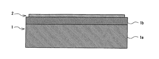
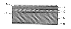
- the organic electronic device shown in FIGS. 1A to 1C includes a substrate 1 and an organic electronic element 2 laminated on one surface of the substrate 1.
- the substrate 1 is an organic electronic device substrate according to an embodiment of the present invention, and includes a metal layer 1a and an insulating layer 1b laminated on at least one surface (organic electronic element lamination surface) side of the metal layer 1a. And have.
- the metal layer 1a is a layer containing a metal as a main component, and iron, titanium, or an alloy thereof is used as the metal.
- a cold-rolled steel sheet a hot-dip galvanized steel sheet (GI), an alloyed hot-dip Zn—Fe-plated steel board (GA), an alloyed hot-dip Zn-5% Al-plated steel sheet (GF),
- GI hot-dip galvanized steel sheet
- GA alloyed hot-dip Zn—Fe-plated steel board
- GF alloyed hot-dip Zn-5% Al-plated steel sheet
- a metal plate such as an electropure galvanized steel plate (EG), an electro Zn—Ni plated steel plate, a titanium plate, or a galvalume steel plate can be used.
- the metal plate is preferably non-chromated, but may be chromated or untreated. Further, the metal plate may be subjected to a phosphoric acid-based chemical conversion treatment.
- a metal plate that has been subjected to chemical conversion treatment with an acidic aqueous solution containing colloidal silica and an aluminum phosphate salt compound is preferable.
- an acidic aqueous liquid containing colloidal silica and an aluminum phosphate salt compound is used as the chemical conversion treatment liquid, the surface of the zinc-based plating layer is etched by the acidic aqueous liquid. At the same time, as shown in FIG.
- the acidic aqueous solution contains a water-soluble resin such as poly
- a rust prevention layer 1d may be provided on both surfaces of the metal layer 1a.
- the durability of the substrate 1 is improved and long-term use is possible.
- the reaction layer 1c is laminated on the organic electronic element lamination surface of the anticorrosion layer 1d.
- the average thickness of the metal layer 1a is not particularly limited, but can be 0.3 mm or more and 2.0 mm or less.
- the insulating layer 1b is a layer having insulating properties, and preferably contains a synthetic resin as a main component.
- a synthetic resin a thermosetting resin, a thermoplastic resin, a photocurable resin, or the like can be used.
- a thermosetting resin or other resin for example, a thermoplastic resin
- a thermosetting agent are used.
- the insulating layer 1b may contain a pigment or the like in addition to the synthetic resin.
- thermosetting resin is not particularly limited, and examples thereof include a phenol resin, an epoxy resin, a urea resin, a melamine resin, a diallyl phthalate resin, and the like.
- a main component of the insulating layer 1b polyester is used. preferable.
- the insulating layer 1b can be formed from a thermosetting resin composition by adding the below-mentioned thermosetting agent to the insulating layer 1b.
- Polyester is obtained by a condensation reaction between a polybasic acid such as a dibasic acid and a polyhydric alcohol.
- the polybasic acid used as a raw material for polyester include ⁇ , ⁇ -unsaturated dibasic acids such as maleic acid, maleic anhydride, fumaric acid, itaconic acid, itaconic anhydride; phthalic acid, phthalic anhydride, halogenated Phthalic anhydride, isophthalic acid, terephthalic acid, tetrahydrophthalic acid, tetrahydrophthalic anhydride, hexahydrophthalic acid, hexahydroisophthalic acid, hexahydroterephthalic acid, cyclopentadiene-maleic anhydride adduct, succinic acid, malonic acid, glutar Acid, adipic acid, sebacic acid, 1,10-decanedicarboxylic acid, 2,6-naphthalenedicarboxylic acid, 2,
- polyhydric alcohol used as a raw material for polyester examples include ethylene glycols such as ethylene glycol, diethylene glycol and polyethylene glycol, propylene glycols such as propylene glycol, dipropylene glycol and polypropylene glycol, 2-methyl-1,3- Propanediol, 1,3-butanediol, adduct of bisphenol A and propylene oxide or ethylene oxide, glycerin, trimethylolpropane, 1,3-propanediol, 1,2-cyclohexane glycol, 1,3-cyclohexane glycol, 1 , 4-cyclohexane glycol, para-xylene glycol, bicyclohexyl-4,4'-diol, 2,6-decalin glycol, tris (2-hydroxyethyl) ) Isocyanurate, and the like, but not particularly limited.
- amino alcohols such as ethanolamine may be used. Only one kind of these polyhydric
- the polyester may be modified with an epoxy resin, diisocyanate, dicyclopentadiene or the like, if necessary.
- the resin used for the insulating layer 1b various commercially available products can be suitably used.
- various commercially available products for example, Byron (registered trademark) 23CS, Byron (registered trademark) 29CS, Byron (registered trademark) 29XS.
- Byron (registered trademark) 20SS, Byron (registered trademark) 29SS manufactured by Toyobo Co., Ltd.
- the insulating layer 1b is not dissolved in an organic solvent, but there is a possibility that the solvent used at the time of molding enters the layer and changes such as swelling. In order to suppress this, even when a thermosetting resin is used as the synthetic resin, it is effective to increase the degree of curing (crosslinking density) of the insulating layer 1b by containing a predetermined amount of a thermosetting agent.
- thermosetting agent for example, in the isocyanate type, Millionate (registered trademark) N, Coronate (registered trademark) T, Coronate (registered trademark) HL, Coronate (registered trademark) 2030, Sprasec 3340, Daltsec 1350, Daltsec 2170
- melamine resin such as Daltosec 2280 (manufactured by Nippon Polyurethane Industry Co., Ltd.), Nicarak (registered trademark) MS-11, Nicarac (registered trademark) MS21 (manufactured by Sanwa Chemical Co., Ltd.), Super Becamine (registered trademark) ) L-105-60, Super Becamine (registered trademark) J-820-60 (above, manufactured by DIC
- content of a synthetic resin in insulating layer 1b As a minimum of content of a synthetic resin in insulating layer 1b, 26.5 mass% is preferred and 36.0 mass% is more preferred. On the other hand, as an upper limit of content of a synthetic resin, 80.0 mass% is preferable and 56.3 mass% is more preferable.
- content of a synthetic resin refers to the ratio of content of a synthetic resin with respect to the total mass of solid content (synthetic resin, a thermosetting agent, a pigment, etc.) in the insulating layer 1b. The same applies to the contents of the thermosetting agent described later.
- thermosetting agent As a minimum of content of a thermosetting agent in insulating layer 1b, 10.0 mass% is preferred and 20.0 mass% is more preferred. On the other hand, the upper limit of the content of the thermosetting agent is preferably 50.0% by mass. By setting it as content of such a thermosetting agent, the insulating layer 1b can be formed easily and reliably.
- the upper limit of the mass ratio is preferably 1.0.
- the insulating layer 1b is made of polyester or a thermosetting resin
- volume shrinkage occurs during curing, or the surface shape is greatly undulated or uneven due to the influence of the solvent volatile gas component.
- the surface shape can be flattened because the shrinkage of the synthetic resin and the desorption of the solvent gas can be promoted.
- the addition of a pigment can increase the surface roughness and form many protrusions on the surface. Therefore, it is necessary to adjust the particle size and the amount of the pigment to be mixed.
- the average particle diameter of the pigment is preferably 100 nm or more and 300 nm or less. Moreover, as content of the pigment in the insulating layer 1b, 30 to 50 mass% is preferable.
- pigments white pigments, titanium oxide, calcium carbonate, zinc oxide, barium sulfate, lithopone, lead white and other inorganic pigments, black pigments, organic pigments such as aniline black and nigrosine, carbon black, iron black and other inorganic pigments There are pigments. There are other organic pigments, but since the purpose of adding the pigment in the present invention is to control the surface shape, it is preferable to use an inorganic pigment.
- pigment commercially available products may be used as long as the above-mentioned preferable average particle diameter is satisfied.
- JR-806 average particle diameter of 0.25 ⁇ m
- Taipei registered trademark manufactured by Ishihara Sangyo Co., Ltd.
- CR-50 average particle size 0.25 ⁇ m
- R930 average particle size 0.25 ⁇ m
- a pigment dispersant may be added to the insulating layer 1b.
- Suitable pigment dispersants are water-soluble acrylic resins, water-soluble styrene acrylic resins, nonionic surfactants, or combinations thereof.
- the lower limit of the average thickness of the insulating layer 1b is preferably 5 ⁇ m and more preferably 10 ⁇ m.
- the upper limit of the average thickness of the insulating layer 1b is preferably 30 ⁇ m, and more preferably 20 ⁇ m.
- the resistivity of the insulating layer 1b is preferably 10 10 ⁇ cm or more. “Resistivity” is a value measured according to JIS-K-7194 (1994).
- K value The organic electronic device does not have an uneven peak with a K value calculated by the following formula (1) of ⁇ 0.07 or less on one surface of the substrate.
- K [f (x + dx) ⁇ 2f (x) + f (x ⁇ dx)] / dx 2 (1)
- x is a peak position of unevenness when a line roughness analysis is performed at intervals of 2.45 nm with respect to a 10 ⁇ m square range on one side of the substrate, and f (x) is a surface at x The unevenness height [nm].
- Dx is a minute change amount of x.
- This K value represents the “curvature” of the so-called protrusion (uneven peak) on the surface of the substrate 1, and the greater the K value, that is, the greater the curvature, the lower the sharpness of the protrusion.
- the present inventors have found that steep protrusions on the surface of the substrate cause the concentration of electrolysis and short-circuit the element, and eliminate the peak of unevenness with the K value of ⁇ 0.07 or less. It has been found that by setting the K value on the surface of the material to be more than ⁇ 0.07, protrusions that cause a short circuit of the element can be eliminated.
- This K value can be adjusted, for example, by polishing described in a method for manufacturing an organic electronic device described later.
- dx can be a calculation interval of x, specifically, about 2 nm to 10 nm.
- the upper limit of the peak of unevenness where the K value on one side of the substrate is ⁇ 0.05 or less is preferably 5, more preferably 3, and even more preferably 1. It is particularly preferred not to have it.
- Organic electronic element 2 examples include an organic EL element, a solar cell element, a liquid crystal display element, a thin film transistor, a touch panel element, and an electronic paper element.
- the organic EL element examples include an element in which an anode, an organic light emitting layer, and a cathode are laminated in this order.
- the organic EL element other electron injection layers, electron transport layers, hole transport layers, and the like may be laminated as appropriate.
- a well-known thing can be used for the element which comprises an organic EL element.
- the anode for example, a transparent electrode using indium tin oxide (ITO) can be used.
- the cathode for example, an electrode using metal or indium zinc oxide (IZO) can be used.
- ⁇ -NPD can be used as the main component of the organic light emitting layer.
- the organic electronic device can be suitably used for organic EL lighting.
- the organic electronic element 2 for example, by using a solar cell element in which an anode, a potential donor, an electron acceptor, and a cathode are laminated in this order, the organic electronic device can be suitably used for an organic solar cell.
- the organic electronic device can be obtained, for example, by a manufacturing method including a step of preparing the substrate 1 and a step of laminating the organic electronic element 2 on one surface of the substrate 1.
- the insulating layer 1b is laminated by applying the insulating layer forming composition to the organic electronic element lamination surface side of the metal layer 1a and heating to form the substrate 1.
- This insulating layer forming composition is preferably liquid. That is, the insulating layer forming composition preferably contains a solvent.
- the solvent used for the insulating layer forming composition is not particularly limited as long as it can dissolve or disperse each component to be contained in the insulating layer forming composition.
- the solvent include alcohols such as methanol, ethanol, n-propanol, isopropanol, n-butanol, isobutanol, and ethylene glycol; ketones such as acetone, methyl ethyl ketone, methyl isobutyl ketone, and cyclohexanone; toluene, benzene, xylene, Aromatic hydrocarbons such as Solvesso (registered trademark) 100 (produced by ExxonMobil), Solvesso (registered trademark) 150 (produced by ExxonMobil); Aliphatic hydrocarbons such as hexane, heptane, and octane; Ethyl acetate, Acetic acid Examples thereof include esters such as butyl.
- the lower limit of the solid content concentration of the insulating layer forming composition is preferably 20% by mass, and more preferably 40% by mass.
- the upper limit of the solid content concentration of the composition for forming an insulating layer is preferably 80% by mass, and more preferably 70% by mass.
- the method for applying and heating (drying and baking) the insulating layer forming composition is not particularly limited, and a known method can be appropriately employed.
- the coating method include a bar coater method, a roll coater method, a curtain flow coater method, a spray method, and a spray ringer method.
- a bar coater method, a roll coater method, And the spray ringer method is preferred.
- the lower limit of the heating temperature of the insulating layer forming composition is preferably 190 ° C, more preferably 200 ° C.
- an upper limit of heating temperature 250 degreeC is preferable and 240 degreeC is more preferable.
- strength of the insulating layer 1b may become inadequate.
- the heating temperature exceeds the above upper limit, by preventing the solvent from evaporating vigorously, the convection due to the organic solvent evaporated in the vicinity of the metal plate surface evaporates, and as a result, evaporated in the vicinity of the surface of the metal layer 1a. Convection due to the solvent is likely to occur, and the smoothness of the surface of the insulating layer 1b may be impaired.
- heating temperature points out ultimate plate temperature (Peak Metal Temperature: PMT).
- reaction layer 1c may be formed before applying the insulating layer forming composition to the metal layer 1a. Moreover, you may provide the antirust layer 1d on the surface of the metal layer 1a.
- the organic electronic element laminated surface (the surface of the insulating layer 1b) of the substrate 1 may be subjected to a polishing treatment.
- the polishing method include chemical polishing (CMP), electrolytic polishing, and mechanical polishing.
- CMP chemical polishing
- electrolytic polishing electrolytic polishing
- mechanical polishing from the viewpoint of removing fine irregularities, a chemical electropolishing method using, for example, silica, alumina, ceria, titania, zirconia, germania or the like as an abrasive is preferable.
- Organic electronic device lamination process In this step, the organic electronic element 2 is laminated on the organic electronic element lamination surface of the substrate 1.
- this lamination method a conventionally known method can be used.
- polyester Toyobo “Byron (registered trademark) 200” (glass transition point Tg: 53 ° C., number average molecular weight) 75 parts by mass in terms of solid content and 25 parts by mass of melamine resin ("Super Becamine (registered trademark) J-820-60" from DIC) in terms of solid content are obtained. It was. The amount of the mixed solvent of xylene and cyclohexanone was adjusted so that the total solid content of the polyester and melamine resin was 58% by mass.
- an electrogalvanized metal plate having a plate thickness of 0.8 mm and a zinc plating adhesion amount on each side of the metal plate of 20 g / m 2 was prepared.
- the paint A is applied to one surface of this metal plate with a bar coater, heated for 2 minutes so that the ultimate plate temperature (PMT) is 220 ° C., and an insulating layer having an average thickness of 15 ⁇ m is formed.
- PMT ultimate plate temperature
- the surface of the insulating layer was smoothed by performing chemical mechanical polishing on the substrate.
- the substrate was set in a holder to which a substrate mounting suction pad of the polishing apparatus was attached, and set on the polishing pad attached to the surface plate of the polishing apparatus with the insulating layer facing down.
- Granular alumina (average particle diameter is about 100 nm) is used as an abrasive, pressure is 65 g / cm 2 , rotation distance per rotation is 1 m, each rotation speed of substrate and surface plate is 50 rpm, chemical mechanical polishing for 10 minutes Went.
- the polishing depth was 3 ⁇ m in Example 2, 6 ⁇ m in Example 3, and 9 ⁇ m in Example 4 in terms of polishing amount.
- the surface shape was evaluated in a plurality of 10 ⁇ m square ranges, and a line roughness analysis was performed at intervals of 2.45 nm, and a K value of the above formula (1) was obtained for each peak of the unevenness.
- the number of peaks having a K value of ⁇ 0.07 or less and the number of peaks of ⁇ 0.05 or less are shown in Table 1, respectively.
- an organic EL element was laminated on the surface of the substrate.
- This organic EL element includes an ITO layer (average thickness: 50 nm), a PEDOT / PSS layer (average thickness: 60 nm), an NPD layer (average thickness: 80 nm), an Alq layer (average thickness: 50 nm), and a LiF layer. (0.8 nm), an AgMg layer (10 nm), and an IZO layer (100 nm) are laminated in this order.
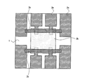
- the planar shape of the organic EL element is a 2 mm square shape shown in FIG. 2, and four of these were stacked on a 30 mm square substrate.
- a transparent sealing glass was laminated on the surface of the organic EL element.
- the specific lamination conditions of the organic EL element are as follows. First, the substrate and the sealing glass were cleaned in a clean booth (class 100) in a clean room (class 1,000). Organic solvents (EL standard products), organic alkaline solutions (EL standard products), ultrapure water (18 M ⁇ , TOC: 10 ppb or less) are used as cleaning chemicals, and ultrasonic cleaning machines (40 kHz and 950 kHz) are used as cleaning equipment. UV ozone cleaner and vacuum desiccator were used. As cleaning procedures, wet cleaning (ultra pure water, organic alkaline solution, and a combination of an organic solvent and ultrasonic waves), drying (vacuum degassing), and dry cleaning (UV ozone) were performed in this order.
- each layer is deposited at a vacuum degree of 1 to 2 ⁇ 10 4 Pa, a deposition rate of 1 to 2 ⁇ / s (dopant is 0.01 ⁇ / s, LiF is 0.1 ⁇ / s), and an organic EL element is laminated. did.
- the inside of the glove box (H 2 O and O 2 concentration of less than 10 ppm is bonded to the sealing glass, taken out of the glow box and irradiated with UV, and then subjected to 3 ° C. at 80 ° C. as a heat treatment.
- Sealing glass was laminated by storing for a long time, using a 10 mm square product made by Dynic as a getter and using a UV curable epoxy resin from ThreeBond as a sealing material.
- the arithmetic average roughness of the substrate surfaces of Examples 1 to 9 and Comparative Examples 1 to 3 are all 25 nm or less. However, in Comparative Examples 1 to 3, the number of elements that can be confirmed to emit light is less than 2, and a short circuit is likely to occur. In particular, in Comparative Example 2, the number of light emitting elements is 1 although the arithmetic average roughness is as small as 2.9 nm. That is, it can be seen that the provision of only the arithmetic average roughness of the substrate surface is insufficient for preventing short circuit.
- Examples 1 to 9 examples 2, 5, and 9 in which the number of peaks with a K value of ⁇ 0.05 or less is 0, the number of light emitting elements is 4, and no short circuit occurs. That is, it can be seen that short-circuiting can be prevented more reliably by reducing the peak of the K value of ⁇ 0.05 or less.
- the organic electronic device and the organic electronic device substrate are excellent in manufacturing yield by suppressing the occurrence of element short circuit, and thus can be suitably used for various applications.
Landscapes
- Physics & Mathematics (AREA)
- Optics & Photonics (AREA)
- Electromagnetism (AREA)
- Engineering & Computer Science (AREA)
- General Engineering & Computer Science (AREA)
- Electroluminescent Light Sources (AREA)
- Planar Illumination Modules (AREA)
- Photovoltaic Devices (AREA)
- Laminated Bodies (AREA)
Abstract
Description
K=[f(x+dx)-2f(x)+f(x-dx)]/dx2・・・(1)
上記式(1)中、xは基板の一方の面の10μm四方の範囲に対し2.45nm間隔で線粗さ分析を行った時の凹凸のピーク位置であり、f(x)はxにおける表面凹凸高さ[nm]である。また、dxはxの微小変化量である。
基板1は、本発明の一実施形態である有機電子デバイス用基板であって、金属層1aと、この金属層1aの少なくとも一方の面(有機電子素子積層面)側に積層される絶縁層1bとを有する。
金属層1aは、金属を主成分とする層であり、この金属としては、鉄、チタン、又はこれらの合金が用いられる。具体的には、金属層1aとしては、冷延鋼板、溶融純亜鉛めっき鋼板(GI)、合金化溶融Zn-Feめっき鋼板(GA)、合金化溶融Zn-5%Alめっき鋼板(GF)、電気純亜鉛めっき鋼板(EG)、電気Zn-Niめっき鋼板、チタン板、ガルバリウム鋼板等の金属板を使用できる。
絶縁層1bは、絶縁性を有する層であり、合成樹脂を主成分とすることが好ましい。この合成樹脂としては、熱硬化性樹脂、熱可塑性樹脂、光硬化性樹脂等を用いることができるが、これらの中でも熱硬化性樹脂、又はその他の樹脂(例えば熱可塑性樹脂)と熱硬化剤とを組み合わせて用いることが好ましい。また、絶縁層1bは、合成樹脂の他に、顔料等を含有してもよい。
当該有機電子デバイスは、上記基板の一方の面に下記式(1)で算出されるK値が-0.07以下となる凹凸のピークを有しない。
K=[f(x+dx)-2f(x)+f(x-dx)]/dx2・・・(1)
有機電子素子2としては、例えば有機EL素子、太陽電池素子、液晶表示素子、薄膜トランジスタ、タッチパネル素子、電子ペーパー素子等が挙げられる。
当該有機電子デバイスは、例えば基板1を用意する工程、及び基板1の一方の面に有機電子素子2を積層する工程を備える製造方法により得ることができる。
本工程では、金属層1aの有機電子素子積層面側への絶縁層形成用組成物の塗布及び加熱により、絶縁層1bを積層し、基板1を形成する。この絶縁層形成用組成物は液状であることが好ましい。つまり、絶縁層形成用組成物は溶媒を含むことが好ましい。
本工程では、基板1の有機電子素子積層面に有機電子素子2を積層する。この積層方法としては、従来公知の方法を使用することができる。
キシレン(沸点:140℃)とシクロヘキサノン(沸点:156℃)とを等量ずつ混合した溶媒に、ポリエステル(東洋紡社の「バイロン(登録商標)200」(ガラス転移点Tg:53℃、数平均分子量Mn:3000))を固形分換算で75質量部、メラミン樹脂(DIC社の「スーパーベッカミン(登録商標)J-820-60」)を固形分換算で25質量部加えて、塗料Aを得た。なお、ポリエステルとメラミン樹脂との合計固形分が58質量%となるようにキシレンとシクロヘキサノンとの混合溶媒の量を調整した。
キシレン(沸点:140℃)とシクロヘキサノン(沸点:156℃)とを等量ずつ混合した溶媒に、ポリエステル(東洋紡社の「バイロン(登録商標)200」(Tg:53℃、Mn:3000))を固形分換算で21.75質量部、メラミン樹脂(DIC社の「スーパーベッカミン(登録商標)J-820-60」)を固形分換算で7.25質量部、酸化チタン粒子(石原産業社の「タイペーク(登録商標)CR-50」(平均粒子径0.25μm))を固形分換算で29.00質量部加えて、塗料Bを得た。ポリエステル、メラミン樹脂、及び酸化チタン粒子の合計の固形分が58質量%となるようにキシレンとシクロヘキサノンとの混合溶媒の量を調整した。
キシレン(沸点:140℃)とシクロヘキサノン(沸点:156℃)とを等量ずつ混合した溶媒に、ポリエステル(東洋紡社の「バイロン(登録商標)200」(Tg:53℃、Mn:3000))を固形分換算で26.1質量部、メラミン樹脂(DIC社の「スーパーベッカミン(登録商標)J-820-60」)を固形分換算で8.7質量部、酸化チタン粒子(石原産業社の「タイペーク(登録商標)CR-50」(平均粒子径0.25μm))を固形分換算で23.2質量部加えて、塗料Cを得た。ポリエステル樹脂、メラミン樹脂、及び酸化チタン粒子の合計の固形分が58質量%となるようにキシレンとシクロヘキサノンとの混合溶媒の量を調整した。

本出願は、2015年5月28日出願の日本特許出願(特願2015-109226)に基づくものであり、その内容はここに参照として取り込まれる。
きる。
1a 金属層
1b 絶縁層
1c 反応層
1d 防錆層
2 有機電子素子
2a ITO層
2b PEDOT・PSS層/NPD層/Alq層
2c LiF層/AgMg層
Claims (13)
- 基板及びこの基板の一方の面に積層される有機電子素子を備える有機電子デバイスであって、
上記基板が、金属層と、この金属層の少なくとも一方の面側に積層される絶縁層とを有し、
上記基板の一方の面に下記式(1)で算出されるK値が-0.07以下となる凹凸のピークがないことを特徴とする有機電子デバイス。
K=[f(x+dx)-2f(x)+f(x-dx)]/dx2 ・・・(1)
上記式(1)中、xは基板の一方の面の10μm四方の範囲に対し2.45nm間隔で線粗さ分析を行った時の凹凸のピーク位置であり、f(x)はxにおける表面凹凸高さ[nm]である。また、dxはxの微小変化量である。 - 上記絶縁層が合成樹脂を主成分とする請求項1に記載の有機電子デバイス。
- 上記絶縁層が顔料を含有する請求項2に記載の有機電子デバイス。
- 上記顔料が無機顔料であり、顔料の平均粒径が300nm以下、絶縁層における顔料の含有量が50質量%以下である請求項3に記載の有機電子デバイス。
- 上記合成樹脂が熱硬化性樹脂である請求項2に記載の有機電子デバイス。
- 上記合成樹脂が熱硬化性樹脂である請求項3に記載の有機電子デバイス。
- 上記合成樹脂が熱硬化性樹脂である請求項4に記載の有機電子デバイス。
- 上記合成樹脂がポリエステルであり、上記絶縁層が熱硬化剤を含有する請求項2に記載の有機電子デバイス。
- 上記合成樹脂がポリエステルであり、上記絶縁層が熱硬化剤を含有する請求項3に記載の有機電子デバイス。
- 上記合成樹脂がポリエステルであり、上記絶縁層が熱硬化剤を含有する請求項4に記載の有機電子デバイス。
- 上記金属層が鉄、チタン、又はこれらの合金を主成分とする請求項1に記載の有機電子デバイス。
- 有機EL照明又は有機太陽電池に用いられる請求項1に記載の有機電子デバイス。
- 基板及びこの基板の一方の面に積層される有機電子素子を備える有機電子デバイス用の基板であって、
金属層と、この金属層の少なくとも一方の面側に積層される絶縁層とを有し、
一方の面に下記式(1)で算出されるK値が-0.07以下となる凹凸のピークがないことを特徴とする有機電子デバイス用基板。
K=[f(x+dx)-2f(x)+f(x-dx)]/dx2 ・・・(1)
上記式(1)中、xは基板の一方の面の10μm四方の範囲に対し2.45nm間隔で線粗さ分析を行った時の凹凸のピーク位置であり、f(x)はxにおける表面凹凸高さ[nm]である。また、dxはxの微小変化量である。
Priority Applications (3)
| Application Number | Priority Date | Filing Date | Title |
|---|---|---|---|
| CN201680024032.2A CN107535025A (zh) | 2015-05-28 | 2016-05-24 | 有机电子设备和有机电子设备用基板 |
| KR1020177036473A KR20180008762A (ko) | 2015-05-28 | 2016-05-24 | 유기 전자 디바이스 및 유기 전자 디바이스용 기판 |
| US15/568,534 US20180123065A1 (en) | 2015-05-28 | 2016-05-24 | Organic electronic device and substrate for organic electronic device |
Applications Claiming Priority (2)
| Application Number | Priority Date | Filing Date | Title |
|---|---|---|---|
| JP2015109226A JP6125564B2 (ja) | 2015-05-28 | 2015-05-28 | 有機電子デバイス及び有機電子デバイス用基板 |
| JP2015-109226 | 2015-05-28 |
Publications (1)
| Publication Number | Publication Date |
|---|---|
| WO2016190309A1 true WO2016190309A1 (ja) | 2016-12-01 |
Family
ID=57393375
Family Applications (1)
| Application Number | Title | Priority Date | Filing Date |
|---|---|---|---|
| PCT/JP2016/065321 Ceased WO2016190309A1 (ja) | 2015-05-28 | 2016-05-24 | 有機電子デバイス及び有機電子デバイス用基板 |
Country Status (6)
| Country | Link |
|---|---|
| US (1) | US20180123065A1 (ja) |
| JP (1) | JP6125564B2 (ja) |
| KR (1) | KR20180008762A (ja) |
| CN (1) | CN107535025A (ja) |
| TW (1) | TW201709584A (ja) |
| WO (1) | WO2016190309A1 (ja) |
Families Citing this family (5)
| Publication number | Priority date | Publication date | Assignee | Title |
|---|---|---|---|---|
| JP6767945B2 (ja) * | 2017-08-17 | 2020-10-14 | 株式会社神戸製鋼所 | 電子デバイス用金属基板 |
| WO2019202739A1 (ja) * | 2018-04-20 | 2019-10-24 | 堺ディスプレイプロダクト株式会社 | 有機elデバイスおよびその製造方法 |
| JP6867738B2 (ja) * | 2018-04-20 | 2021-05-12 | 堺ディスプレイプロダクト株式会社 | 有機elデバイスの製造方法 |
| JP6942208B2 (ja) * | 2018-04-20 | 2021-09-29 | 堺ディスプレイプロダクト株式会社 | 有機elデバイスおよびその製造方法 |
| JP7066578B2 (ja) * | 2018-09-04 | 2022-05-13 | 株式会社神戸製鋼所 | 有機電子デバイス及び有機電子デバイス用基板 |
Citations (5)
| Publication number | Priority date | Publication date | Assignee | Title |
|---|---|---|---|---|
| JP2002025763A (ja) * | 2000-07-11 | 2002-01-25 | Nisshin Steel Co Ltd | 有機el素子用絶縁基板 |
| JP2004191463A (ja) * | 2002-12-09 | 2004-07-08 | Hitachi Metals Ltd | ディスプレイ用基板及びその製造方法 |
| JP2011108883A (ja) * | 2009-11-18 | 2011-06-02 | Mitsubishi Chemicals Corp | 太陽電池 |
| JP2013084461A (ja) * | 2011-10-11 | 2013-05-09 | Nisshin Steel Co Ltd | 有機el素子用基板及びその製造方法、並びに有機el素子 |
| WO2014157601A1 (ja) * | 2013-03-28 | 2014-10-02 | 株式会社神戸製鋼所 | 金属基板、それを用いたサブストレート型薄膜太陽電池及びトップエミッション型有機el素子 |
Family Cites Families (2)
| Publication number | Priority date | Publication date | Assignee | Title |
|---|---|---|---|---|
| JP6229439B2 (ja) * | 2013-11-05 | 2017-11-15 | 住友ベークライト株式会社 | 金属張積層板、プリント配線基板、および半導体装置 |
| CN204179111U (zh) * | 2014-11-13 | 2015-02-25 | 京东方科技集团股份有限公司 | 一种顶发射白光oled器件和显示装置 |
-
2015
- 2015-05-28 JP JP2015109226A patent/JP6125564B2/ja active Active
-
2016
- 2016-05-24 WO PCT/JP2016/065321 patent/WO2016190309A1/ja not_active Ceased
- 2016-05-24 KR KR1020177036473A patent/KR20180008762A/ko not_active Ceased
- 2016-05-24 US US15/568,534 patent/US20180123065A1/en not_active Abandoned
- 2016-05-24 CN CN201680024032.2A patent/CN107535025A/zh active Pending
- 2016-05-26 TW TW105116370A patent/TW201709584A/zh unknown
Patent Citations (5)
| Publication number | Priority date | Publication date | Assignee | Title |
|---|---|---|---|---|
| JP2002025763A (ja) * | 2000-07-11 | 2002-01-25 | Nisshin Steel Co Ltd | 有機el素子用絶縁基板 |
| JP2004191463A (ja) * | 2002-12-09 | 2004-07-08 | Hitachi Metals Ltd | ディスプレイ用基板及びその製造方法 |
| JP2011108883A (ja) * | 2009-11-18 | 2011-06-02 | Mitsubishi Chemicals Corp | 太陽電池 |
| JP2013084461A (ja) * | 2011-10-11 | 2013-05-09 | Nisshin Steel Co Ltd | 有機el素子用基板及びその製造方法、並びに有機el素子 |
| WO2014157601A1 (ja) * | 2013-03-28 | 2014-10-02 | 株式会社神戸製鋼所 | 金属基板、それを用いたサブストレート型薄膜太陽電池及びトップエミッション型有機el素子 |
Also Published As
| Publication number | Publication date |
|---|---|
| JP6125564B2 (ja) | 2017-05-10 |
| US20180123065A1 (en) | 2018-05-03 |
| TW201709584A (zh) | 2017-03-01 |
| JP2016225091A (ja) | 2016-12-28 |
| CN107535025A (zh) | 2018-01-02 |
| KR20180008762A (ko) | 2018-01-24 |
Similar Documents
| Publication | Publication Date | Title |
|---|---|---|
| JP5656177B2 (ja) | 有機発光素子用基板及びその製造方法 | |
| JP6125564B2 (ja) | 有機電子デバイス及び有機電子デバイス用基板 | |
| JP4383077B2 (ja) | ガスバリア性基板 | |
| JP5715721B2 (ja) | 金属基板 | |
| JP2006044231A (ja) | ガスバリア性フィルム、並びにこれを用いたディスプレイ用基板及びディスプレイ | |
| JP5741489B2 (ja) | ガスバリア性フィルムおよび電子デバイス | |
| JP5928634B2 (ja) | ガスバリア性フィルムおよび電子デバイス | |
| JP6201807B2 (ja) | 有機発光素子の製造方法及び有機発光素子 | |
| JP5487556B2 (ja) | ガスバリア性シート及びその製造方法 | |
| WO2016158678A1 (ja) | 金属基板 | |
| JP7066578B2 (ja) | 有機電子デバイス及び有機電子デバイス用基板 | |
| JP6767945B2 (ja) | 電子デバイス用金属基板 | |
| JP2016195162A (ja) | 金属基板 | |
| KR102338975B1 (ko) | 절연 피막 적층 금속판 및 금속 기판 | |
| JP2008041640A (ja) | 透明導電膜付きフィルムおよびこの透明導電膜付きフィルムからなるディスプレイ用基板、ディスプレイ、液晶表示装置ならびに有機el素子 | |
| JP2017177491A (ja) | 金属基板 | |
| JP2017177490A (ja) | 金属基板 |
Legal Events
| Date | Code | Title | Description |
|---|---|---|---|
| 121 | Ep: the epo has been informed by wipo that ep was designated in this application |
Ref document number: 16800014 Country of ref document: EP Kind code of ref document: A1 |
|
| WWE | Wipo information: entry into national phase |
Ref document number: 15568534 Country of ref document: US |
|
| NENP | Non-entry into the national phase |
Ref country code: DE |
|
| ENP | Entry into the national phase |
Ref document number: 20177036473 Country of ref document: KR Kind code of ref document: A |
|
| 122 | Ep: pct application non-entry in european phase |
Ref document number: 16800014 Country of ref document: EP Kind code of ref document: A1 |