WO2016189426A1 - タッチパネル - Google Patents
タッチパネル Download PDFInfo
- Publication number
- WO2016189426A1 WO2016189426A1 PCT/IB2016/052882 IB2016052882W WO2016189426A1 WO 2016189426 A1 WO2016189426 A1 WO 2016189426A1 IB 2016052882 W IB2016052882 W IB 2016052882W WO 2016189426 A1 WO2016189426 A1 WO 2016189426A1
- Authority
- WO
- WIPO (PCT)
- Prior art keywords
- electrode
- transistor
- layer
- semiconductor layer
- touch panel
- Prior art date
- Legal status (The legal status is an assumption and is not a legal conclusion. Google has not performed a legal analysis and makes no representation as to the accuracy of the status listed.)
- Ceased
Links
Images















Classifications
-
- G—PHYSICS
- G06—COMPUTING OR CALCULATING; COUNTING
- G06F—ELECTRIC DIGITAL DATA PROCESSING
- G06F3/00—Input arrangements for transferring data to be processed into a form capable of being handled by the computer; Output arrangements for transferring data from processing unit to output unit, e.g. interface arrangements
- G06F3/01—Input arrangements or combined input and output arrangements for interaction between user and computer
- G06F3/03—Arrangements for converting the position or the displacement of a member into a coded form
- G06F3/041—Digitisers, e.g. for touch screens or touch pads, characterised by the transducing means
- G06F3/0416—Control or interface arrangements specially adapted for digitisers
- G06F3/0418—Control or interface arrangements specially adapted for digitisers for error correction or compensation, e.g. based on parallax, calibration or alignment
-
- G—PHYSICS
- G02—OPTICS
- G02F—OPTICAL DEVICES OR ARRANGEMENTS FOR THE CONTROL OF LIGHT BY MODIFICATION OF THE OPTICAL PROPERTIES OF THE MEDIA OF THE ELEMENTS INVOLVED THEREIN; NON-LINEAR OPTICS; FREQUENCY-CHANGING OF LIGHT; OPTICAL LOGIC ELEMENTS; OPTICAL ANALOGUE/DIGITAL CONVERTERS
- G02F1/00—Devices or arrangements for the control of the intensity, colour, phase, polarisation or direction of light arriving from an independent light source, e.g. switching, gating or modulating; Non-linear optics
- G02F1/01—Devices or arrangements for the control of the intensity, colour, phase, polarisation or direction of light arriving from an independent light source, e.g. switching, gating or modulating; Non-linear optics for the control of the intensity, phase, polarisation or colour
- G02F1/13—Devices or arrangements for the control of the intensity, colour, phase, polarisation or direction of light arriving from an independent light source, e.g. switching, gating or modulating; Non-linear optics for the control of the intensity, phase, polarisation or colour based on liquid crystals, e.g. single liquid crystal display cells
- G02F1/133—Constructional arrangements; Operation of liquid crystal cells; Circuit arrangements
- G02F1/1333—Constructional arrangements; Manufacturing methods
- G02F1/13338—Input devices, e.g. touch panels
-
- G—PHYSICS
- G06—COMPUTING OR CALCULATING; COUNTING
- G06F—ELECTRIC DIGITAL DATA PROCESSING
- G06F3/00—Input arrangements for transferring data to be processed into a form capable of being handled by the computer; Output arrangements for transferring data from processing unit to output unit, e.g. interface arrangements
- G06F3/01—Input arrangements or combined input and output arrangements for interaction between user and computer
- G06F3/03—Arrangements for converting the position or the displacement of a member into a coded form
- G06F3/041—Digitisers, e.g. for touch screens or touch pads, characterised by the transducing means
- G06F3/0412—Digitisers structurally integrated in a display
-
- G—PHYSICS
- G06—COMPUTING OR CALCULATING; COUNTING
- G06F—ELECTRIC DIGITAL DATA PROCESSING
- G06F3/00—Input arrangements for transferring data to be processed into a form capable of being handled by the computer; Output arrangements for transferring data from processing unit to output unit, e.g. interface arrangements
- G06F3/01—Input arrangements or combined input and output arrangements for interaction between user and computer
- G06F3/03—Arrangements for converting the position or the displacement of a member into a coded form
- G06F3/041—Digitisers, e.g. for touch screens or touch pads, characterised by the transducing means
- G06F3/0416—Control or interface arrangements specially adapted for digitisers
- G06F3/0418—Control or interface arrangements specially adapted for digitisers for error correction or compensation, e.g. based on parallax, calibration or alignment
- G06F3/04182—Filtering of noise external to the device and not generated by digitiser components
-
- G—PHYSICS
- G06—COMPUTING OR CALCULATING; COUNTING
- G06F—ELECTRIC DIGITAL DATA PROCESSING
- G06F3/00—Input arrangements for transferring data to be processed into a form capable of being handled by the computer; Output arrangements for transferring data from processing unit to output unit, e.g. interface arrangements
- G06F3/01—Input arrangements or combined input and output arrangements for interaction between user and computer
- G06F3/03—Arrangements for converting the position or the displacement of a member into a coded form
- G06F3/041—Digitisers, e.g. for touch screens or touch pads, characterised by the transducing means
- G06F3/044—Digitisers, e.g. for touch screens or touch pads, characterised by the transducing means by capacitive means
-
- G—PHYSICS
- G06—COMPUTING OR CALCULATING; COUNTING
- G06F—ELECTRIC DIGITAL DATA PROCESSING
- G06F3/00—Input arrangements for transferring data to be processed into a form capable of being handled by the computer; Output arrangements for transferring data from processing unit to output unit, e.g. interface arrangements
- G06F3/01—Input arrangements or combined input and output arrangements for interaction between user and computer
- G06F3/03—Arrangements for converting the position or the displacement of a member into a coded form
- G06F3/041—Digitisers, e.g. for touch screens or touch pads, characterised by the transducing means
- G06F3/044—Digitisers, e.g. for touch screens or touch pads, characterised by the transducing means by capacitive means
- G06F3/0443—Digitisers, e.g. for touch screens or touch pads, characterised by the transducing means by capacitive means using a single layer of sensing electrodes
-
- G—PHYSICS
- G06—COMPUTING OR CALCULATING; COUNTING
- G06F—ELECTRIC DIGITAL DATA PROCESSING
- G06F3/00—Input arrangements for transferring data to be processed into a form capable of being handled by the computer; Output arrangements for transferring data from processing unit to output unit, e.g. interface arrangements
- G06F3/01—Input arrangements or combined input and output arrangements for interaction between user and computer
- G06F3/03—Arrangements for converting the position or the displacement of a member into a coded form
- G06F3/041—Digitisers, e.g. for touch screens or touch pads, characterised by the transducing means
- G06F3/044—Digitisers, e.g. for touch screens or touch pads, characterised by the transducing means by capacitive means
- G06F3/0446—Digitisers, e.g. for touch screens or touch pads, characterised by the transducing means by capacitive means using a grid-like structure of electrodes in at least two directions, e.g. using row and column electrodes
-
- G—PHYSICS
- G06—COMPUTING OR CALCULATING; COUNTING
- G06F—ELECTRIC DIGITAL DATA PROCESSING
- G06F2203/00—Indexing scheme relating to G06F3/00 - G06F3/048
- G06F2203/041—Indexing scheme relating to G06F3/041 - G06F3/045
- G06F2203/04102—Flexible digitiser, i.e. constructional details for allowing the whole digitising part of a device to be flexed or rolled like a sheet of paper
-
- G—PHYSICS
- G06—COMPUTING OR CALCULATING; COUNTING
- G06F—ELECTRIC DIGITAL DATA PROCESSING
- G06F2203/00—Indexing scheme relating to G06F3/00 - G06F3/048
- G06F2203/041—Indexing scheme relating to G06F3/041 - G06F3/045
- G06F2203/04103—Manufacturing, i.e. details related to manufacturing processes specially suited for touch sensitive devices
-
- G—PHYSICS
- G06—COMPUTING OR CALCULATING; COUNTING
- G06F—ELECTRIC DIGITAL DATA PROCESSING
- G06F2203/00—Indexing scheme relating to G06F3/00 - G06F3/048
- G06F2203/041—Indexing scheme relating to G06F3/041 - G06F3/045
- G06F2203/04111—Cross over in capacitive digitiser, i.e. details of structures for connecting electrodes of the sensing pattern where the connections cross each other, e.g. bridge structures comprising an insulating layer, or vias through substrate
-
- G—PHYSICS
- G06—COMPUTING OR CALCULATING; COUNTING
- G06F—ELECTRIC DIGITAL DATA PROCESSING
- G06F2203/00—Indexing scheme relating to G06F3/00 - G06F3/048
- G06F2203/041—Indexing scheme relating to G06F3/041 - G06F3/045
- G06F2203/04112—Electrode mesh in capacitive digitiser: electrode for touch sensing is formed of a mesh of very fine, normally metallic, interconnected lines that are almost invisible to see. This provides a quite large but transparent electrode surface, without need for ITO or similar transparent conductive material
Definitions
- One embodiment of the present invention relates to a touch panel.
- one embodiment of the present invention is not limited to the above technical field.
- One embodiment of the invention disclosed in this specification and the like relates to an object, a method, or a manufacturing method.
- One aspect of the present invention relates to a process, a machine, a manufacture, or a composition (composition of matter). Therefore, the technical fields of one embodiment of the present invention disclosed in this specification and the like more specifically include semiconductor devices, display devices, light-emitting devices, power storage devices, memory devices, electronic devices, lighting devices, input devices, input / outputs Devices, their driving methods or their manufacturing methods can be mentioned as examples.
- a touch panel refers to a display device (or display module) equipped with a touch sensor.
- the touch panel may be referred to as a touch screen.
- a touch panel in contrast to a member that does not have a display device and is configured only by a touch sensor, such a member may be referred to as a touch panel.
- a display device equipped with a touch sensor may be called a display device with a touch sensor, a touch panel with a display device, a display module, or the like.
- a full-in-cell touch panel uses, for example, an electrode formed on the element substrate side as an electrode for a touch sensor.
- the hybrid in-cell touch panel (or the display device with the hybrid in-cell touch sensor) ).
- the hybrid in-cell type touch panel uses, for example, an electrode made on the element substrate side and an electrode made on the counter substrate side as electrodes for the touch sensor.
- the hybrid in-cell type touch panel is active in research and development because it can be made thinner and lower in cost than a display device equipped with an external touch sensor (see Patent Document 1).
- Patent Document 1 In addition, in order to further reduce the thickness and cost, research and development of a full-in-cell touch panel is also active (see Patent Document 2).
- Hybrid in-cell type touch panels and full-in-cell type touch panels have been adopted for liquid crystal display devices, and are being put to practical use in smartphones and tablet terminals. Further, it has been attempted to apply the full-in-cell touch panel to an organic EL display device (see Patent Document 3).
- An object of one embodiment of the present invention is to provide a novel touch panel or the like.
- An object of one embodiment of the present invention is to provide a touch panel or the like having a novel structure that can suppress the influence of noise of electrodes constituting an organic EL element on an electrode for touch detection.
- One embodiment of the present invention is a touch panel including a pixel, a touch sensor, and an integration circuit.
- the pixel includes a transistor and a light-emitting element.
- the light-emitting element includes a pixel electrode and a common electrode.
- the touch sensor has a first electrode and a second electrode, and the first electrode has a function of giving a pulse signal, and the second sensor The electrode has a function of detecting a signal corresponding to the pulse signal
- the integration circuit has an operational amplifier, the operational amplifier has a first input terminal and a second input terminal, The input terminal is a touch panel electrically connected to the second electrode, and the second input terminal is electrically connected to the common electrode.
- One embodiment of the present invention is a touch panel including a pixel, a touch sensor, and an integration circuit.
- the pixel includes a transistor and a light-emitting element.
- the light-emitting element includes a current supply line through the transistor.
- the touch sensor includes a first electrode and a second electrode.
- the first electrode has a function of supplying a pulse signal.
- the second electrode The integration circuit has an operational amplifier, the operational amplifier has a first input terminal and a second input terminal, and the first input terminal has a function capable of detecting a signal corresponding to the pulse signal. Is a touch panel electrically connected to the second electrode, and the second input terminal is electrically connected to the current supply line.
- the first electrode and the second electrode are preferably touch panels provided on a substrate side where a transistor is formed.
- a touch panel in which one of the first electrode and the second electrode is an electrode formed in the same layer as a conductive layer included in a transistor is preferable.
- the other of the first electrode and the second electrode is preferably a touch panel provided on the counter substrate side.
- a touch panel in which one of the first electrode and the second electrode is an electrode provided in a layer below the pixel electrode is preferable.
- the touch sensor is preferably a touch panel that is a mutual capacitance method.
- One embodiment of the present invention can provide a novel touch panel or the like.
- one embodiment of the present invention can provide a touch panel or the like having a novel structure that can suppress the influence of noise of electrodes constituting the organic EL element on the electrodes for touch detection.
- FIGS. 3A and 3B are a circuit diagram and a cross-sectional schematic diagram for illustrating one embodiment of the present invention.
- FIGS. FIG. 6 is a schematic diagram for illustrating one embodiment of the present invention.
- FIG. 6 is a schematic diagram for illustrating one embodiment of the present invention.
- FIG. 6 is a schematic diagram for illustrating one embodiment of the present invention.
- FIG. 10 is a schematic perspective view illustrating one embodiment of the present invention.
- FIG. 10 is a schematic perspective view illustrating one embodiment of the present invention.
- FIG. 10 is a block diagram illustrating one embodiment of the present invention.
- FIG. 10 is a block diagram illustrating one embodiment of the present invention.
- FIG. 10 is a cross-sectional view illustrating one embodiment of the present invention.
- FIG. 10 is a cross-sectional view illustrating one embodiment of the present invention.
- FIG. 10 is a cross-sectional view illustrating one embodiment of the present invention.
- FIG. 10 is a cross-sectional view illustrating one embodiment of the present invention.
- FIG. 10 is a cross-sectional view illustrating one embodiment of the present invention.
- FIG. 10 is a cross-sectional view illustrating one embodiment of the present invention.
- FIG. 10 is a cross-sectional view illustrating one embodiment of the present invention.
- FIG. 10 is a cross-sectional view illustrating one embodiment of the present invention.
- FIG. 10 is a cross-sectional view illustrating one embodiment of the present invention.
- FIG. 10 is a cross-sectional view illustrating one embodiment of the present invention.
- FIG. 10 is a cross-sectional view illustrating one embodiment of the present invention.
- FIG. 10 is a cross-sectional view illustrating one embodiment of the present invention.
- FIG. 10 is a cross-sectional view
- FIG. 10 is a cross-sectional view illustrating one embodiment of the present invention.
- FIG. 10 is a cross-sectional view illustrating one embodiment of the present invention.
- FIG. 10 is a cross-sectional view illustrating one embodiment of the present invention.
- FIG. 10 is a cross-sectional view illustrating one embodiment of the present invention.
- FIG. 10 is a cross-sectional view illustrating one embodiment of the present invention.
- FIG. 10 is a cross-sectional view illustrating one embodiment of the present invention.
- FIG. 10 is a cross-sectional view illustrating one embodiment of the present invention.
- FIG. 10 is a cross-sectional view illustrating one embodiment of the present invention.
- 4A and 4B are a top view and cross-sectional views illustrating one embodiment of the present invention.
- FIG. 6 is an energy band structure diagram illustrating one embodiment of the present invention.
- 4A and 4B illustrate one embodiment of the present invention.
- 4A and 4B illustrate one embodiment of the present invention.
- 4A and 4B illustrate one embodiment of the present invention.
- FIG. 10 is a cross-sectional view illustrating one embodiment of the present invention.
- FIG. 6 is a schematic diagram for illustrating one embodiment of the present invention.
- FIG. 6 is a schematic diagram for illustrating one embodiment of the present invention.
- FIG. 6 is a schematic diagram for illustrating one embodiment of the present invention.
- FIG. 6 is a schematic diagram for illustrating one embodiment of the present invention.
- FIG. 6 is a schematic diagram for illustrating one embodiment of the present invention.
- FIG. 6 is a schematic diagram for illustrating one embodiment of the present invention.
- FIG. 6 is a schematic diagram for illustrating one embodiment of the present invention.
- FIG. 6 is a schematic diagram for illustrating one embodiment of the present invention.
- FIG. 6 is a schematic
- film and “layer” may be interchangeable in some cases.
- conductive layer may be changed to the term “conductive film”
- insulating film may be changed to the term “insulating layer”.
- the touch panel which is one embodiment of the present invention is an EL display device including a touch sensor.
- a touch panel includes, for example, an EL element, a transistor for driving the EL element, and an electrode of a touch sensor.
- the circuit diagram in FIG. 1A shows an EL element, a pixel having a transistor for driving the EL element, and an electrode of the touch sensor.
- the pixel 10 in 2 rows and 2 columns, and the electrode 20 and the electrode 30 of a set of touch sensors are illustrated.
- the pixel 10 includes a transistor 11, a transistor 12, and an EL element 13 as an example.
- the pixel 10 is connected to the scanning line 21, the signal line 22, the current supply line 23, and the common electrode line 24.
- the electrode 20 and the electrode 30 can detect the proximity or contact of an object to be detected by a mutual capacitance method. Specifically, a pulse voltage is applied to the electrode 20 functioning as the drive electrode (Tx), and a current flowing through the electrode 30 functioning as the detection electrode (Rx) is detected. The electric field between Tx and Rx is shielded by the presence or absence of a shield such as a finger or a pen, and the capacitance value changes. By detecting the change in the capacitance value based on the change in the current flowing through the detection electrode (Rx), the proximity or contact of the detection target can be detected. The change in current can be detected by an integration circuit.
- FIG. 1B is an example of a schematic cross-sectional view for explaining the arrangement of the structure shown in the circuit diagram of FIG.
- a pair of substrates 41 and 42 are illustrated as an example.
- the transistor 12, the EL element 13, the current supply line 23, and the partition wall layer 18 are illustrated on the substrate 41.
- the EL element 13 includes, for example, a pixel electrode 15, a light emitting layer 16, and a common electrode 17.
- the common electrode 17 corresponds to the above-described common electrode line 24 and can function as a cathode of the EL element 13. Further, the pixel electrode 15 can function as an anode of the EL element 13.
- an electrode 20 that functions as a drive electrode (Tx) and an electrode 30 that functions as a detection electrode (Rx) are provided between the substrate 41 and the EL element 13, as an example.
- the electrodes 20 and 30 may be formed on the substrate 42 and / or the substrate 43, and can be applied to a hybrid in-cell touch panel or a full-in-cell touch panel depending on the position of the electrodes. In the following discussion, an example applied to a full-in-cell type touch panel will be described for easy understanding.
- the transistor 12 has a function of flowing current to the EL element 13 in accordance with the gate potential.
- the transistor 12 includes an electrode functioning as a gate, an electrode functioning as a source or a drain, and a semiconductor layer. Note that although not illustrated in FIG. 1B, an electrode functioning as a source or a drain of the transistor 11 is connected to the gate of the transistor 12. Details of the configuration of the transistors 11 and 12 will be described later.
- the electrodes 20 and 30 are provided on the substrate 41 side where the transistor 12 is formed.
- the electrodes 20 and 30 can be an electrode functioning as a source or a drain of the transistor 11 or a conductive layer provided in the same layer as an electrode formed in the same layer as the gate of the transistor 12.
- the electrodes 20 and 30 can be conductive layers provided in the same layer as the pixel electrode 15. With such a structure, an electrode that functions as a separate touch sensor can be formed without requiring a new process.
- one electrode of the touch sensor is provided on the substrate 41 side, and the other electrode of the touch sensor is provided on the substrate 42 side.
- the electrode 30 functioning as the detection electrode (Rx) is disposed close to the common electrode 17 formed on one surface. Therefore, the electrode 30 is easily affected by noise generated in the common electrode 17.
- electrode 30 detects a change of a signal obtained by a change in capacitance C MC in the integration circuit, to detect a touch.
- the signal obtained by the electrode 30 is affected by noise, it becomes difficult to determine whether the change in the signal acquired by the integration circuit is due to touch detection or noise, and accurate touch detection is difficult. .
- the current supply line arranged close to the common electrode line is also easily affected by noise generated in the common electrode 17.
- the current supply line is formed of a conductive layer made of the same material as that of the electrode 30, the parasitic capacitance component and the resistance component are similar, so that the noise waveform can be easily similar.
- the integration circuit that detects a change in the signal of the electrode 30 has an operational amplifier.
- the operational amplifier amplifies and outputs the potential difference between the two input terminals.
- the integrating circuit operates by connecting an input signal to one input terminal and applying a reference voltage to the other input terminal. Therefore, when a signal obtained by the electrode 30 affected by noise is input to one input terminal of the input signal, the noise is amplified, and accurate touch detection becomes difficult.
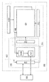
- ⁇ Configuration example 1 of touch panel> the configuration of the schematic diagram illustrated in FIG. In FIG. 2, the electrode 20 functioning as the drive electrode (Tx), the electrode 30 functioning as the detection electrode (Rx), the common electrode 17, and the common electrode line 24 shown in FIGS.
- the integration circuit 500 and the level shifter circuit 501 are shown.
- the integration circuit 500 includes a capacitor 502 and a switch 503 as an example.
- the output of the integrating circuit 500 is illustrated as a signal AMP_OUT.
- a signal given to the electrode 20 functioning as the drive electrode (Tx) through the level shifter circuit 510 is illustrated as a signal TS_IN.
- a signal waveform 20_W applied to the electrode 20 is illustrated.
- a signal waveform 30_W obtained by the electrode 30 is illustrated.
- a noise waveform 24_W of the common electrode line 24 is illustrated.
- Touch detection on the touch panel gives a pulse signal as signal TS_IN. Then, a waveform 20_W that is a pulse signal is input to the electrode 20 that functions as the drive electrode (Tx). The change in the signal of the electrode 20 is transmitted to the electrode 30 functioning as the detection electrode (Rx) by the capacitive component between the electrodes (Tx ⁇ Rx). A signal waveform 30 ⁇ / b> _W obtained by the electrode 30 changes due to a change in capacitance between the electrodes due to the presence or absence of touch. A change in the signal waveform 30_W can be detected by an integration circuit, and a signal AMP_OUT including the presence or absence of touch can be output.
- the electrode 30 functioning as a detection electrode (Rx) is connected to one input terminal of the operational amplifier 501.
- the common electrode line 24 connected to the common electrode 17 is connected to the other input terminal of the operational amplifier 501. That is, in one embodiment of the present invention, a signal having the noise waveform 24_W is supplied to the reference voltage of the operational amplifier 501 included in the integration circuit 500. With such a configuration, when noise generated in the common electrode 17 also appears in the electrode 30 functioning as the detection electrode (Rx), the output of the operational amplifier 501 can be obtained as a signal in which noise is canceled. Therefore, in one embodiment of the present invention, the signal AMP_OUT can be obtained while suppressing the influence of noise.
- FIG. 3 shows a schematic diagram in the case where the reference voltage input to the other input terminal of the operational amplifier 501 included in the integrating circuit 500 is a fixed voltage VREF .
- a waveform 30_W having noise is input to one input terminal of an operational amplifier 501 included in the integration circuit 500, and a waveform 520_W having no noise is input to the other input terminal.
- the operational amplifier 501 has a function of amplifying and outputting a signal difference between input terminals. Therefore, the signal-noise ratio (S / N ratio) becomes small, and there is a possibility that the touch detection cannot be performed normally.
- a signal having noise is input to one input terminal of the operational amplifier 501 included in the integration circuit 500 and noise is input to the other input terminal.
- a signal will be input.
- the operational amplifier 501 has a function of amplifying and outputting a signal difference between input terminals. Therefore, both noises are canceled out, the S / N ratio is increased, and touch detection can be performed normally.
- FIG. 4A shows a case where a plurality of common electrodes 17 in FIG. 2 are provided.
- the common electrode illustrated in FIG. 4A is divided into a plurality of electrodes 17_1 to 17_4.
- the plurality of electrodes 17_1 to 17_4 are preferably arranged in parallel with the electrode 30 that is a detection electrode of the touch sensor.
- FIG. 4A illustrates electrodes 30_1 to 30_4 which are detection electrodes of the touch sensor, and the electrode 30_1 and the electrode 17_1 arranged in parallel are connected to an input terminal of an operational amplifier included in the integration circuit 500_1.
- the electrode 30_2 and the electrode 17_2, the electrode 30_3 and the electrode 17_3, and the electrode 30_4 and the electrode 17_4 are connected to input terminals of operational amplifiers included in the integration circuits 500_2 to 500_4.
- the integrating circuits 500_1 to 30_4 output output signals AMP_OUT1 to AMP_OUT4, respectively.
- the output signals AMP_OUT1 to AMP_OUT4 can cancel the noise and suppress the influence of the noise, similarly to the configuration described in FIG.
- the electrode 17_1 and the electrode 30_1 are provided so as to overlap, for example. Therefore, the electrode 17_1 and the electrode 30_1 are affected by noise having the same waveform. That is, by dividing the region and inputting the waveform of the common electrode input to the integration circuit, it is possible to easily add noise having the same waveform to the common electrode and the detection electrode. Therefore, it is possible to make it easier to cancel the noise of the common electrode and the noise of the touch detection electrode.
- FIG. 4B shows a different structure from FIG. 4B includes a plurality of electrodes 17_1 to 17_4 and integration circuits 500_1 to 500_4 as in FIG. 4A.
- the electrode 17_1 is connected to the integration circuits 500_1 and 500_2, and the electrode 17_3 is connected to the integration circuits 500_3 and 500_4.
- the electrode 17_1 and the electrode 17_2, and the electrode 17_3 and the electrode 17_4 are adjacent to each other, and are easily affected by noise having the same waveform. Therefore, the same effect as in FIG. 2 can be obtained even when an electrode serving as an adjacent common electrode is connected to the input terminals of the integration circuits 500_1 to 500_4 so as to have a reference voltage.
- the touch panel of one embodiment of the present invention is a reference voltage in an integration circuit that inputs a voltage of an electrode for touch detection and a reference voltage to an input terminal of an operational amplifier and detects a change in a capacitance value due to touch detection.
- the input terminal for supplying the voltage is connected to the common electrode constituting the organic EL element.
- FIG. 37 in addition to the electrode 20 functioning as the drive electrode (Tx), the electrode 30 functioning as the detection electrode (Rx), and the current supply line 23 shown in FIGS. 1 (A) and (B), An integration circuit 500 and a level shifter circuit 510 are shown.
- the integration circuit 500 includes a capacitor 502 and a switch 503 as an example.
- the output of the integrating circuit 500 is illustrated as a signal AMP_OUT.
- a signal given to the electrode 20 functioning as the drive electrode (Tx) through the level shifter circuit 510 is illustrated as a signal TS_IN.
- FIG. 37 a signal waveform 20_W applied to the electrode 20 is shown.
- a signal waveform 30_W obtained by the electrode 30 is illustrated.
- a noise waveform 23_W of the current supply line 23 is illustrated.
- Touch detection on the touch panel gives a pulse signal as signal TS_IN. Then, a waveform 20_W that is a pulse signal is input to the electrode 20 that functions as the drive electrode (Tx). The change in the signal of the electrode 20 is transmitted to the electrode 30 functioning as the detection electrode (Rx) by the capacitive component between the electrodes (Tx ⁇ Rx). A signal waveform 30 ⁇ / b> _W obtained by the electrode 30 changes due to a change in capacitance between the electrodes due to the presence or absence of a touch. A change in the signal waveform 30_W can be detected by an integration circuit, and a signal AMP_OUT including the presence or absence of touch can be output.
- the electrode 30 functioning as the detection electrode (Rx) is connected to one input terminal of the operational amplifier 501.
- the current supply line 23 is connected to the other input terminal of the operational amplifier 501. That is, in one embodiment of the present invention, a signal having the noise waveform 23_W is supplied to the reference voltage of the operational amplifier 501 included in the integration circuit 500. With such a configuration, when noise generated in the current supply line 23 also appears in the electrode 30 functioning as the detection electrode (Rx), the output of the operational amplifier 501 can be obtained as a signal in which noise is canceled. Therefore, in one embodiment of the present invention, the signal AMP_OUT can be obtained while suppressing the influence of noise.
- FIG. 38 schematically illustrates the case where the reference voltage input to the other input terminal of the operational amplifier 501 included in the integration circuit 500 is the fixed voltage VREF .
- a waveform 30_W having noise is input to one input terminal of an operational amplifier 501 included in the integration circuit 500, and a waveform 520_W having no noise is input to the other input terminal.
- the operational amplifier 501 has a function of amplifying and outputting a signal difference between input terminals. Therefore, the signal-noise ratio (S / N ratio) becomes small, and there is a possibility that the touch detection cannot be performed normally.
- a signal having noise is input to one input terminal of the operational amplifier 501 included in the integration circuit 500 and noise is input to the other input terminal.
- a signal will be input.
- the operational amplifier 501 has a function of amplifying and outputting a signal difference between input terminals. Therefore, both noises are canceled out, the S / N ratio is increased, and touch detection can be performed normally.
- FIG. 39A shows a case where a plurality of current supply lines 23 in FIG. 37 are provided.
- the current supply line illustrated in FIG. 39A is divided into a plurality of current supply lines 23_1 to 23_4.
- the plurality of current supply lines 23_1 to 23_4 are preferably arranged in parallel with the electrode 30 that is a detection electrode of the touch sensor.
- FIG. 39A illustrates electrodes 30_1 to 30_4 which are detection electrodes of the touch sensor, and the electrode 30_1 and the current supply line 23_1 which are arranged in parallel are the input terminals of the operational amplifier included in the integration circuit 500_1. Connected.
- the electrode 30_2 and the current supply line 23_2, the electrode 30_3 and the current supply line 23_3, and the electrode 30_4 and the current supply line 23_4 are connected to input terminals of operational amplifiers included in the integration circuits 500_2 to 500_4.
- the integrating circuits 500_1 to 500_4 output output signals AMP_OUT1 to AMP_OUT4, respectively.
- the output signals AMP_OUT1 to AMP_OUT4 can cancel the noise and suppress the influence of the noise, similarly to the configuration described in FIG.
- the current supply line 23_1 and the electrode 30_1 are provided so as to overlap with each other. Therefore, the current supply line 23_1 and the electrode 30_1 are affected by noise having the same waveform. That is, by dividing the region and inputting the waveform of the current supply line input to the integration circuit, it is possible to easily add noise of the same waveform to the current supply line and the detection electrode. Therefore, it is possible to more easily cancel the noise of the current supply line and the noise of the touch detection electrode.
- FIG. 39B shows a structure different from that in FIG. 39B includes a plurality of current supply lines 23_1 to 23_4 and integration circuits 500_1 to 500_4 as in FIG. 39A.
- the current supply line 23_1 is connected to the integration circuits 500_1 and 500_2, and the current supply line 23_3 is connected to the integration circuits 500_3 and 500_4.
- the current supply line 23_1 and the current supply line 23_2, and the current supply line 23_3 and the current supply line 23_4 are adjacent to each other, and are easily affected by noise having the same waveform. Therefore, the same effect as in FIG. 37 can be obtained even when an electrode serving as an adjacent common electrode is connected to the input terminals of the integration circuits 500_1 to 500_4 so as to have a reference voltage.
- the touch panel of one embodiment of the present invention is a reference voltage in an integration circuit that inputs a voltage of an electrode for touch detection and a reference voltage to an input terminal of an operational amplifier and detects a change in a capacitance value due to touch detection. Is connected to a current supply line for supplying a current to the organic EL element. With this configuration, the noise of the electrode for touch detection on which the noise of the current supply line is superimposed can be canceled, so that the influence of noise can be suppressed.
- FIG. 5A is a schematic perspective view of the touch panel 310 of one embodiment of the present invention.
- the touch panel 310 is a full-in-cell type touch panel.
- FIG. 5B is a schematic perspective view of FIG. 5A developed. For the sake of clarity, only representative components are shown.
- the touch panel 310 includes a substrate 371 and a substrate 372 provided to face each other.
- a display portion 381, a drive circuit 382, a wiring 383, a drive circuit 384, and the like are provided over the substrate 371.
- a conductive layer 385 is formed in the x direction.
- a plurality of conductive layers 386 and the like are formed orthogonal to the conductive layer 385, that is, in the y direction.
- the display unit 381 has at least a plurality of pixels.
- the pixel includes a transistor and an EL element.
- the driving circuit 382 can be, for example, a scanning line driving circuit which is a display driving circuit for performing display.
- the substrate 371 is provided with an FPC 373 that is electrically connected to the wiring 383.
- 5A and 5B show an example in which an IC 374 is provided on the FPC 373.
- FIG. 5A and 5B show an example in which an IC 374 mounted on the FPC 373 by the COF (Chip On Film) method is provided.
- the IC 374 for example, a signal line driver circuit which is a display driver circuit for performing display and an IC having a function as a touch sensor driver circuit for processing a signal obtained from the conductive layer 385 provided in the y direction are applied. it can.
- the wiring 383 has a function of supplying signals and power to the display portion 381, the drive circuit 382, the drive circuit 384, and the like.
- the signal and power are input to the wiring 383 from the outside or the IC 374 through the FPC 373.
- the drive circuit 384 can be, for example, a touch sensor drive circuit for driving the conductive layer 385 provided in the x direction.
- the drive circuit 384 can be omitted because the IC 374 also has the function.
- the touch sensor includes a conductive layer 385 and a conductive layer 386 provided on the substrate 371. That is, the conductive layer 385 or the conductive layer 386 can function as a drive electrode (Tx) or a detection electrode (Rx). The touch sensor can detect using a capacitor formed between the conductive layer 385 and the conductive layer 386.
- a member such as a transistor for performing display, an EL element, and a driver circuit, an electrode for performing a touch sensor, and a member such as a driver circuit are arranged on one substrate side (here, the substrate 371 side). ) Can only be placed. For this reason, it is possible to share functions such as integrating the display drive circuit and the touch sensor drive circuit.
- FIG. 6A is a schematic perspective view of the touch panel 320 of one embodiment of the present invention, which has a structure different from that in FIG.
- the touch panel 320 is a hybrid in-cell touch panel.
- FIG. 6B is a schematic perspective view of FIG. 6A developed. For the sake of clarity, only representative components are shown.
- the touch panel 320 includes a substrate 371 and a substrate 372 provided to face each other as in FIGS. 5A and 5B illustrated as a full-in-cell type.
- a display portion 381, a drive circuit 382, a wiring 383, a drive circuit 384, and the like are provided over the substrate 371 as in the case of FIGS. 5A and 5B illustrated as a full-in-cell type. Further, in the display portion 381, a conductive layer 385 is formed in the x direction as in the case of FIGS. 5A and 5B illustrated as a full-in-cell type.
- a plurality of conductive layers 386 and the like are formed orthogonal to the conductive layer 385, that is, in the y direction, unlike FIGS. 5A and 5B illustrated as a full-in-cell type. Further, unlike FIGS. 5A and 5B which are illustrated as a full-in-cell type, a conductive layer 387 and the like are formed over the substrate 372.
- the conductive layer 387 is electrically connected to any of the plurality of conductive layers 386.
- the conductive layer 387 is electrically connected to the FPC 373 through the connection portion 388 and the connection portion 389 provided on the substrate 371 side.
- the display portion 381 has at least a plurality of pixels as in FIGS. 5A and 5B illustrated as a full-in-cell type.
- the pixel includes a transistor and an EL element.
- the driving circuit 382 can be, for example, a scanning line driving circuit which is a display driving circuit for performing display, similarly to FIGS. 5A and 5B illustrated as a full-in-cell type.
- the substrate 371 is provided with an FPC 373 that is electrically connected to the wiring 383, similarly to FIGS. 5A and 5B illustrated as a full-in-cell type.
- 6A and 6B illustrate an example in which an IC 374 is provided on the FPC 373.
- an example in which an IC 374 mounted by a COF (Chip On Film) method is provided on the FPC 373 is the same as in FIGS. 5A and 5B illustrated as a full-in-cell type.
- a signal line driver circuit which is a display driver circuit for performing display and an IC having a function as a touch sensor driver circuit for processing a signal obtained from the conductive layer 385 provided in the y direction are applied. it can.
- the wiring 383 has a function of supplying signals and power to the display portion 381, the driving circuit 382, the driving circuit 384, and the like, as in FIGS. 5A and 5B illustrated as a full-in-cell type.
- the signal and power are input to the wiring 383 from the outside or the IC 374 through the FPC 373.
- the drive circuit 384 can be a touch sensor drive circuit for driving the conductive layer 385 provided in the x direction, similarly to FIGS. 5A and 5B illustrated as a full-in-cell type.
- the drive circuit 384 can be omitted because the IC 374 also has the function.
- the touch sensor includes a conductive layer 385 provided on the substrate 371 and a conductive layer 386 provided on the substrate 372, unlike FIGS. 5A and 5B illustrated as a full-in-cell type. That is, the conductive layer 385 or the conductive layer 386 can function as a drive electrode (Tx) or a detection electrode (Rx). The touch sensor can detect using a capacitor formed between the conductive layer 385 and the conductive layer 386.
- the electrodes constituting the touch sensor are formed on different substrates, members such as a transistor, an EL element, and a drive circuit for performing display, and a touch sensor are provided.
- Members such as electrodes and driving circuits can be arranged only on one substrate side (here, the substrate 371 side). For this reason, it is possible to share functions such as integrating the display drive circuit and the touch sensor drive circuit.
- Fig. 7 shows a block diagram of a touch panel including peripheral circuits.
- the touch panel 400 includes a display unit 401 and a touch sensor unit 402.
- the touch panel 400 includes a display drive circuit 411, a touch sensor drive circuit 412, and a timing controller 413 as an example of peripheral circuits for driving the display unit 401 and the touch sensor unit 402.
- a power supply circuit for generating a power supply voltage necessary for the display portion 401 and the touch sensor portion 402 may be provided.
- the display driving circuit 411 includes a scanning line driving circuit 414 and a signal line driving circuit 415 as an example.
- the scan line driver circuit 414 and the signal line driver circuit 415 can sequentially drive pixels (not shown) provided in a matrix in the display portion 401 to control display.
- a plurality of scanning line driver circuits 414 and signal line driver circuits 415 may be provided and controlled by dividing an area of a pixel to be displayed.
- the definition of an image to be displayed, the signal writing speed, and the like can be increased.
- the touch sensor driving circuit 412 includes analog circuits 416A and 416B and a digital signal processing circuit 417 as an example.
- the analog circuits 416A and 416B are circuits that mainly handle analog signals.
- the digital signal processing circuit 417 is a circuit that mainly handles digital signals.
- the analog circuit 416A has a function of applying a pulse voltage to the drive electrode (Tx) side of the touch sensor unit 402 as an example.
- Examples of the analog circuit 416A include a level shifter circuit, a buffer circuit, and the like.
- the analog circuit 416B has, for example, a function of receiving an analog signal from the detection electrode (Rx) side of the touch sensor unit 402 and converting it into a digital signal.
- Examples of the analog circuit 416B include an integration circuit, a sample hold circuit, and an A / D (analog / digital) converter.
- the digital signal processing circuit 417 is a circuit that performs signal processing such as noise removal of the digital signal output from the analog circuit 416B, touch position detection, and touch position tracking processing.
- a dedicated circuit for performing signal processing such as ASIC (Application Specific Integrated Circuit) or FPGA (Field Programmable Gate Array) can be manufactured and used. Data obtained by signal processing in the digital signal processing circuit 417 can be output to the host controller 420 outside the touch panel 400.
- the timing controller 413 is a circuit that receives a video signal or the like from the host controller 420 and generates a signal for controlling the display driving circuit 411, such as a clock signal, a vertical synchronization signal, a horizontal synchronization signal, or the like.
- the timing controller 413 is a circuit that receives a signal from the host controller 420 and generates, for example, a signal for controlling the touch sensor driving circuit 412.
- Various signals received from the external host controller 420 are input to the timing controller 4 through an interface such as DVI (Digital Visual Interface), LVDS (Low Voltage Differential Signaling), RSDS (Reduced Swing Differential Signaling) 13 and the like. .
- DVI Digital Visual Interface
- LVDS Low Voltage Differential Signaling
- RSDS Reduced Swing Differential Signaling
- the host controller 420 is a circuit for inputting / outputting various signals to / from the peripheral circuit of the touch panel.
- the host controller 420 includes, for example, an arithmetic circuit and a frame memory, and is a circuit that inputs and outputs signals to and from the touch panel 400 or other devices.
- a part of the circuits included in the display driver circuit 411, the touch sensor driver circuit 412, and the timing controller 413 described above is provided with a touch panel 400 by using an integrated circuit (IC: Integrated Circuit) manufactured on a silicon substrate. It can be provided on a substrate or an FPC (Flexible Printed Circuit) connected to a substrate provided with the touch panel 400. Therefore, the IC 440 illustrated in FIG. 7 is illustrated as a configuration including a signal line driver circuit 415, an analog circuit 416B, a digital signal processing circuit 417, and a timing controller 413 in the block of the touch panel 400.
- IC integrated circuit
- FIG. 7 is illustrated as a configuration including a signal line driver circuit 415, an analog circuit 416B, a digital signal processing circuit 417, and a timing controller 413 in the block of the touch panel 400.
- the function of driving the display unit 401 and the function of driving the touch sensor unit 402 are incorporated into one IC, so that the number of ICs mounted on the touch panel 400 can be reduced. Cost can be reduced.
- 8A, 8B, and 8C are schematic diagrams for explaining an example in which an IC is mounted on a touch panel.
- the touch panel module 400A includes a substrate 451, a counter substrate 452, a plurality of FPCs 453, IC 454, IC 455, and the like.
- a display portion 456, a touch sensor portion 457, and a scan line driver circuit 458 are provided between the substrate 451 and the counter substrate 452.
- the IC 454 and the IC 455 are mounted on the substrate 451 by a mounting method such as a COG (Chip On Glass) method.
- the IC 454 includes a circuit that functions as the signal line driver circuit 415 in the IC 440 described with reference to FIG.
- the IC 454 includes circuits that function as the analog circuit 416B, the digital signal processing circuit 417, and the timing controller 413 in the IC 440 described with reference to FIG. Signals are supplied to the IC 454 and the IC 455 from the outside via the FPC 453. A signal can be output from the IC 454 or the IC 455 to the outside via the FPC 453.
- FIG. 8A shows an example of a structure in which two scanning line driver circuits 458 are provided so as to sandwich the display portion 456.
- a configuration having an IC 455 in addition to the IC 454 is shown.
- Such a configuration can be preferably used when the pixels of the display portion 456 are arranged so as to have extremely high definition.
- 8B shows an example in which one IC 454A and one FPC 453 are mounted on the touch panel module 400B.
- the IC 454A includes a circuit that functions as the signal line driver circuit 415, the analog circuit 416B, the digital signal processing circuit 417, and the timing controller 413 in the IC 440 described with reference to FIG.
- 8B illustrates an example in which the scan line driver circuit 458 is arranged along the side closer to the FPC 453 out of the two short sides of the display portion 456.
- FIG. 8C shows an example of a configuration having a PCB (Printed Circuit Board) 459 on which an IC 460 or the like having a part of the functions of the ICs 454 and 454A described in FIGS. 8A and 8B is mounted. Yes.
- the ICs 454B and IC455B on the substrate 451 and the PCB 459 are electrically connected by the FPC 453.
- ICs 454, 454A, 454B, IC455, and IC455B may be mounted on the FPC 453 instead of on the substrate 451.
- C454, 454A, 454B, IC455, and IC455B may be mounted on the FPC 453 by a mounting method such as a COF (Chip On Film) method or a TAB (Tape Amounted Bonding) method.
- the configuration in which the FPC 453 and the ICs 454 and 454A are arranged on the short side of the display portion 456 can be narrowed, for example, a smartphone, a mobile phone, or a tablet terminal It can use suitably for electronic devices, such as. 8C can be preferably used for, for example, a television device, a monitor device, a tablet terminal, a laptop personal computer, or the like.
- cross-sectional view of touch panel of one embodiment of the present invention will be described using a plurality of examples of a full-in-cell touch panel and a hybrid in-cell touch panel.
- the following cross-sectional configuration examples 1 to 4 correspond to full-in-cell type touch panels, and cross-sectional configuration examples 5 to 6 correspond to hybrid in-cell type touch panels.
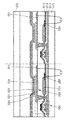
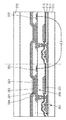
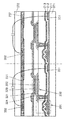
- FIG. 9 shows a cross-sectional configuration example of a region including two subpixels.
- the structure in FIG. 9 includes a bottom emission type light emitting device that emits light to the substrate (element substrate) side where the transistor 201 and the like are formed.
- the touch panel has a light emitting element 202.
- the light-emitting element 202 has a structure in which a conductive layer 321 (pixel electrode), an EL layer 322, and a conductive layer 323 (common electrode) are stacked. Further, an optical adjustment layer 324 may be provided between the conductive layer 321 and the conductive layer 323. Light from the light emitting element 202 is emitted to the substrate 371 side.
- the conductive layer 321 has a function as a pixel electrode and a function as an anode of the light-emitting element 202.
- the conductive layer 323 has a function as a shared electrode and a function as a cathode of the light-emitting element 202.
- a transistor or the like is not illustrated on the substrate 372 (counter substrate) side, a transistor or the like may be formed. Further, a desiccant or the like may be provided between the light emitting element 202 and the substrate 372. Or it is good also as a structure which reinforces impact resistance while filling the fillers, such as a thermosetting resin, etc., preventing the penetration
- the conductive layer 321 preferably has translucency.
- the conductive layer 323 preferably has reflectivity.
- a colored layer 231 is provided on the substrate 371 side with respect to the light emitting element 202.
- the colored layer 231 is provided over the insulating layer 213.
- One of the conductive layer 351 and the conductive layer 352 functions as one electrode of the touch sensor, and the other functions as the other electrode of the touch sensor.
- the conductive layer 351 is formed on the same surface as the conductive layer 321.
- the conductive layer 352 is formed on the same surface as one of the two gate electrodes included in the transistor 201. Therefore, a touch panel can be manufactured without increasing manufacturing steps.
- detection can be performed using the capacitance generated between the conductive layer 351 and the conductive layer 352 on the substrate 371 side.
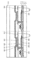
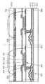
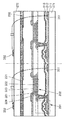
- FIG. 10 is different in that the position of the conductive layer 352 in FIG. 9 is different.
- one of the conductive layer 352 and the gate electrode of the transistor 201 is provided between the insulating layer 212 and the insulating layer 213.
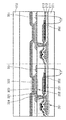
- the conductive layer 352 may be disposed so as to overlap at least one of the conductive layer 321, the optical adjustment layer 324, the EL layer 322, the conductive layer 323, and the coloring layer 231. Further, as illustrated in FIG. 12, the conductive layer 352 may be disposed so as not to overlap any of the conductive layer 321, the optical adjustment layer 324, the EL layer 322, the conductive layer 323, and the coloring layer 231.
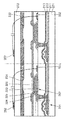
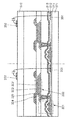
- FIG. 13 shows an example in which both the conductive layer 351 and the conductive layer 352 constituting the touch sensor are formed on the same surface as the conductive layer 321.
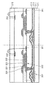
- FIG. 14 is a cross-sectional configuration example of a touch panel including a top emission type light emitting device that emits light to the substrate 372 side.
- the conductive layer 321 has reflectivity
- the conductive layer 323 has translucency
- the conductive layer 323 has an opening at least in a portion overlapping with a part of the conductive layer 351.
- the conductive layer 323 may have a slit or an opening, or may have a comb shape.
- the conductive layer 351 and the conductive layer 352 are formed on the same surface as the conductive layer 321.
- FIG. 14 shows an example in which detection is performed using a capacitance generated between the conductive layer 351 disposed in one subpixel and the conductive layer 352 disposed in the other subpixel.
- FIG. 15 shows an example in which the EL layer 322 is formed by a separate coating method. At this time, as illustrated in FIG. 15, by covering the end portion of the EL layer 322 with the conductive layer 323, diffusion of impurities into the EL layer 322 is suppressed, and reliability can be improved.
- FIG. 15 shows an example in which the colored layer 231 and the like are not provided.
- FIG. 16 shows an example in which the conductive layer 352 constituting the touch sensor is formed on one surface on the substrate 372 (counter substrate) side in the configuration of FIG.
- the structure shown in FIG. 16 is a touch panel including a top emission type light emitting device.
- the conductive layer 351 constituting the touch sensor is formed on the same surface as the conductive layer 321.
- the conductive layer 323 has an opening at least in a portion overlapping with part of the conductive layer 351.
- a conductive layer 352 constituting the touch sensor is formed on the other surface on the substrate 372 (counter substrate) side.
- FIG. 18 shows an example in which the EL layer 322 is formed by the painting method in the configuration of FIG.
- FIG. 19 shows an example in which the EL layer 322 is formed by a separate coating method in the configuration of FIG.
- the conductive layer 352 constituting the touch sensor is formed on one surface on the substrate 372 (counter substrate) side, and the conductive layer 351 constituting the touch sensor is the substrate 372 (counter substrate).
- the transistor 201 is formed on the same surface as the source or drain electrode of the transistor 201.
- 20 is a touch panel including a top emission type light emitting device.
- the conductive layer 351 constituting the touch sensor is formed on the same surface as the conductive layer 321.
- the conductive layer 323 has an opening at least in a portion overlapping with part of the conductive layer 351.
- a conductive layer 352 constituting the touch sensor is formed on the other surface on the substrate 372 (counter substrate) side.
- FIG. 22 shows an example in which the EL layer 322 is formed by a coating method in the configuration of FIG.
- FIG. 23 shows an example in which the EL layer 322 is formed by a separate coating method in the configuration of FIG.
- the conductive layer 351 and the conductive layer 352 may be provided on the substrate 372 side so as to be an on-cell type.
- a material having a flat surface can be used for a substrate included in the touch panel.
- a material that transmits the light is used for the substrate from which light from the display element is extracted.
- materials such as glass, quartz, ceramic, sapphire, and organic resin can be used. It is also possible to apply a single crystal semiconductor substrate made of silicon or silicon carbide, a polycrystalline semiconductor substrate, a compound semiconductor substrate such as silicon germanium, an SOI substrate, etc., and a semiconductor element provided on these substrates May be used as a substrate.
- the sixth generation (1500 mm ⁇ 1850 mm), the seventh generation (1870 mm ⁇ 2200 mm), the eighth generation (2200 mm ⁇ 2400 mm), the ninth generation (2400 mm ⁇ 2800 mm), and the tenth generation
- a large-area substrate such as (2950 mm ⁇ 3400 mm
- a flexible substrate may be used as the substrate, and a transistor, a capacitor, or the like may be formed directly over the flexible substrate.
- the touch panel can be reduced in weight and thickness. Furthermore, a flexible touch panel can be realized by using a flexible substrate having a thickness.
- alkali-free glass barium borosilicate glass, alumino borosilicate glass, or the like can be used.
- the material having flexibility and transparency to visible light examples include, for example, glass having a thickness having flexibility, polyester resins such as polyethylene terephthalate (PET) and polyethylene naphthalate (PEN), and polyacrylonitrile resin. , Polyimide resin, polymethyl methacrylate resin, polycarbonate (PC) resin, polyethersulfone (PES) resin, polyamide resin, cycloolefin resin, polystyrene resin, polyamideimide resin, polyvinyl chloride resin, polytetrafluoroethylene (PTFE) resin Etc.
- a material having a low coefficient of thermal expansion for example, polyamideimide resin, polyimide resin, PET, or the like can be suitably used.
- a substrate in which glass fiber is impregnated with an organic resin, or a substrate in which an inorganic filler is mixed with an organic resin to reduce the thermal expansion coefficient can be used. Since a substrate using such a material is light in weight, a touch panel using the substrate can be lightweight.
- the substrate on the side from which light emission is not extracted does not have to be translucent, in addition to the above-described substrate, a metal substrate, a ceramic substrate, or a semiconductor substrate using a metal material or an alloy material Etc. can also be used.
- a metal material or an alloy material is preferable because it has high thermal conductivity and can easily conduct heat to the entire sealing substrate, which can suppress a local temperature increase of the touch panel.
- the thickness of the metal substrate is preferably 10 ⁇ m to 200 ⁇ m, and more preferably 20 ⁇ m to 50 ⁇ m.
- the material constituting the metal substrate is not particularly limited, and for example, aluminum, copper, nickel, or an alloy of metals such as an aluminum alloy or stainless steel can be suitably used.
- a substrate that has been subjected to insulation treatment by oxidizing the surface of the conductive substrate or forming an insulating film on the surface may be used.
- the insulating film may be formed by using a coating method such as a spin coating method or a dip method, an electrodeposition method, a vapor deposition method, or a sputtering method, or it is left in an oxygen atmosphere or heated, or an anodic oxidation method.
- a coating method such as a spin coating method or a dip method, an electrodeposition method, a vapor deposition method, or a sputtering method, or it is left in an oxygen atmosphere or heated, or an anodic oxidation method.
- an oxide film may be formed on the surface of the substrate.
- a layer using the above-mentioned material is a hard coat layer (for example, a silicon nitride layer) that protects the surface of the touch panel from scratches, or a layer of a material that can disperse pressure (for example, An aramid resin layer etc.) etc. may be laminated
- water permeability of a film containing nitrogen and silicon such as a silicon nitride film or a silicon oxynitride film, or a film containing nitrogen and aluminum such as an aluminum nitride film
- An insulating film with low property may be included.
- the substrate can be used by laminating a plurality of layers.
- the barrier property against water and oxygen can be improved and a highly reliable touch panel can be obtained.
- a substrate in which a glass layer, an adhesive layer, and an organic resin layer are stacked from the side close to the display element can be used.
- the thickness of the glass layer is 20 ⁇ m or more and 200 ⁇ m or less, preferably 25 ⁇ m or more and 100 ⁇ m or less.
- the glass layer having such a thickness can simultaneously realize a high barrier property and flexibility against water and oxygen.
- the thickness of the organic resin layer is 10 ⁇ m or more and 200 ⁇ m or less, preferably 20 ⁇ m or more and 50 ⁇ m or less.
- the transistor includes a conductive layer that functions as a gate electrode, a semiconductor layer, a conductive layer that functions as a source electrode, a conductive layer that functions as a drain electrode, and an insulating layer that functions as a gate insulating layer.
- the above shows the case where a bottom-gate transistor is applied.
- the structure of the transistor included in the touch panel of one embodiment of the present invention there is no particular limitation on the structure of the transistor included in the touch panel of one embodiment of the present invention.
- a planar transistor, a staggered transistor, or an inverted staggered transistor may be used.
- a top-gate or bottom-gate transistor structure may be employed.
- gate electrodes may be provided above and below the channel.
- a semiconductor material used for the transistor is not particularly limited, and examples thereof include an oxide semiconductor, silicon, and germanium.
- crystallinity of a semiconductor material used for the transistor there is no particular limitation on the crystallinity of a semiconductor material used for the transistor, and any of an amorphous semiconductor and a semiconductor having crystallinity (a microcrystalline semiconductor, a polycrystalline semiconductor, a single crystal semiconductor, or a semiconductor partially including a crystal region) is used. May be used. It is preferable to use a crystalline semiconductor because deterioration of transistor characteristics can be suppressed.
- a semiconductor material used for the transistor for example, an element belonging to Group 14, a compound semiconductor, or an oxide semiconductor can be used for the semiconductor layer.
- a semiconductor containing silicon, a semiconductor containing gallium arsenide, an oxide semiconductor containing indium, or the like can be used.
- an oxide semiconductor is preferably used for a semiconductor in which a channel of a transistor is formed.
- an oxide semiconductor having a larger band gap than silicon is preferably used. It is preferable to use a semiconductor material with a wider band gap and lower carrier density than silicon because current in an off state of the transistor can be reduced.
- the oxide semiconductor preferably contains at least indium (In) or zinc (Zn). More preferably, an oxide represented by an In-M-Zn oxide (M is a metal such as Al, Ti, Ga, Ge, Y, Zr, Sn, La, Ce, Hf, or Nd) is included.
- M is a metal such as Al, Ti, Ga, Ge, Y, Zr, Sn, La, Ce, Hf, or Nd
- the semiconductor layer has a plurality of crystal parts, and the crystal part has a c-axis oriented substantially perpendicular to the formation surface of the semiconductor layer or the top surface of the semiconductor layer, and there is no grain between adjacent crystal parts.
- An oxide semiconductor film having no boundary is preferably used.
- Such an oxide semiconductor does not have a crystal grain boundary, cracks in the oxide semiconductor film due to stress when the display panel is bent is suppressed. Therefore, such an oxide semiconductor can be favorably used for a touch panel that is flexible and curved.
- the charge accumulated in the capacitor through the transistor can be held for a long time.
- the driving circuit can be stopped while maintaining the gradation of an image displayed in each display region. As a result, a display device with extremely reduced power consumption can be realized.
- the semiconductor layer is expressed by an In-M-Zn oxide containing at least indium (In), zinc (Zn), and M (metal such as Al, Ti, Ga, Y, Zr, La, Ce, Sn, or Hf). It is preferable to include a film to be formed. In addition, in order to reduce variation in electrical characteristics of the transistor including the oxide semiconductor, a stabilizer is preferably included together with the transistor.
- the stabilizer examples include gallium (Ga), tin (Sn), hafnium (Hf), aluminum (Al), zirconium (Zr), and the like, including the metals described in M above.
- Other stabilizers include lanthanoids such as lanthanum (La), cerium (Ce), praseodymium (Pr), neodymium (Nd), samarium (Sm), europium (Eu), gadolinium (Gd), terbium (Tb). ), Dysprosium (Dy), holmium (Ho), erbium (Er), thulium (Tm), ytterbium (Yb), lutetium (Lu), and the like.
- an oxide semiconductor included in the semiconductor layer for example, an In—Ga—Zn-based oxide, an In—Al—Zn-based oxide, an In—Sn—Zn-based oxide, an In—Hf—Zn-based oxide, an In— La-Zn oxide, In-Ce-Zn oxide, In-Pr-Zn oxide, In-Nd-Zn oxide, In-Sm-Zn oxide, In-Eu-Zn oxide In-Gd-Zn-based oxide, In-Tb-Zn-based oxide, In-Dy-Zn-based oxide, In-Ho-Zn-based oxide, In-Er-Zn-based oxide, In-Tm -Zn oxide, In-Yb-Zn oxide, In-Lu-Zn oxide, In-Sn-Ga-Zn oxide, In-Hf-Ga-Zn oxide, In-Al- Ga-Zn-based oxide, In-Sn-Al-Zn-based oxide, In-Sn-Hf-Zn
- the In—Ga—Zn-based oxide means an oxide containing In, Ga, and Zn as main components, and the ratio of In, Ga, and Zn is not limited. Moreover, metal elements other than In, Ga, and Zn may be contained.
- the semiconductor layer and the conductive layer may have the same metal element among the above oxides. Manufacturing costs can be reduced by using the same metal element for the semiconductor layer and the conductive layer. For example, manufacturing costs can be reduced by using metal oxide targets having the same metal composition. In addition, when a metal oxide target having the same metal composition is used, an etching gas or an etching solution for processing the oxide semiconductor film can be used in common. However, the semiconductor layer and the conductive layer may have different compositions even if they have the same metal element. For example, a metal element in a film may be detached during a manufacturing process of a transistor and a capacitor to have a different metal composition.
- the atomic ratio of In and M excluding Zn and O is preferably 25 atomic% when the sum of In and M is 100 atomic%. Higher, M is less than 75 atomic%, more preferably In is higher than 34 atomic%, and M is less than 66 atomic%.
- the semiconductor layer has an energy gap of 2 eV or more, preferably 2.5 eV or more, more preferably 3 eV or more. In this manner, off-state current of a transistor can be reduced by using an oxide semiconductor with a wide energy gap.
- the thickness of the semiconductor layer is 3 nm to 200 nm, preferably 3 nm to 100 nm, and more preferably 3 nm to 50 nm.
- an In-M-Zn oxide is formed.
- the atomic ratio of the metal elements of the sputtering target used for is preferably satisfying In ⁇ M and Zn ⁇ M.
- In: M: Zn 1: 1: 1: 1
- In: M: Zn 1: 1: 1.2
- the atomic ratio of the semiconductor layer to be formed includes a variation of plus or minus 40% of the atomic ratio of the metal element contained in the sputtering target as an error.
- the semiconductor layer an oxide semiconductor film with low carrier density is used.
- the semiconductor layer has a carrier density of 1 ⁇ 10 17 pieces / cm 3 or less, preferably 1 ⁇ 10 15 pieces / cm 3 or less, more preferably 1 ⁇ 10 13 pieces / cm 3 or less, more preferably 1 ⁇ 10 9.
- An oxide semiconductor film of 11 / cm 3 or less is used.
- a transistor having an appropriate composition may be used depending on required semiconductor characteristics and electrical characteristics (such as field-effect mobility and threshold voltage) of a transistor.
- the semiconductor layer in order to obtain the required semiconductor characteristics of the transistor, it is preferable that the semiconductor layer have appropriate carrier density, impurity concentration, defect density, atomic ratio of metal element to oxygen, interatomic distance, density, and the like. .
- the concentration of silicon or carbon in the semiconductor layer is 2 ⁇ 10 18 atoms / cm 3 or less, preferably 2 ⁇ 10 17 atoms / cm 3 or less.
- the concentration of alkali metal or alkaline earth metal obtained by secondary ion mass spectrometry is set to 1 ⁇ 10 18 atoms / cm 3 or less, preferably 2 ⁇ 10 16 atoms / cm 3 or less.
- the concentration of alkali metal or alkaline earth metal in the semiconductor layer is set to 1 ⁇ 10 18 atoms / cm 3 or less, preferably 2 ⁇ 10 16 atoms / cm 3 or less.
- the nitrogen concentration obtained by secondary ion mass spectrometry is preferably 5 ⁇ 10 18 atoms / cm 3 or less. .
- the semiconductor layer may have a non-single crystal structure, for example.
- the non-single crystal structure includes, for example, a CAAC-OS (C Axis Aligned-Crystalline Oxide Semiconductor) described later, a polycrystalline structure, a microcrystalline structure described later, or an amorphous structure.
- CAAC-OS C Axis Aligned-Crystalline Oxide Semiconductor
- the amorphous structure has the highest density of defect states
- the CAAC-OS has the lowest density of defect states.
- the semiconductor layer may have an amorphous structure, for example.
- An oxide semiconductor film having an amorphous structure has, for example, disordered atomic arrangement and no crystal component.
- an amorphous oxide film has, for example, a completely amorphous structure and does not have a crystal part.
- the semiconductor layer may be a mixed film including an amorphous structure region, a microcrystalline structure region, a polycrystalline structure region, a CAAC-OS region, or a single crystal structure.
- the mixed film may include two or more of an amorphous structure region, a microcrystalline structure region, a polycrystalline structure region, a CAAC-OS region, and a single crystal structure region.
- the mixed film has a stacked structure of two or more of an amorphous structure region, a microcrystalline structure region, a polycrystalline structure region, a CAAC-OS region, and a single crystal structure region. May have.
- silicon is preferably used for a semiconductor in which a transistor channel is formed.
- amorphous silicon may be used as silicon, it is particularly preferable to use silicon having crystallinity.
- microcrystalline silicon, polycrystalline silicon, single crystal silicon, or the like is preferably used.
- polycrystalline silicon can be formed at a lower temperature than single crystal silicon, and has higher field effect mobility and higher reliability than amorphous silicon.
- the aperture ratio of the pixel can be improved.
- the gate driver circuit and the source driver circuit can be formed over the same substrate as the pixel, and the number of components included in the electronic device can be reduced.
- ⁇ Conductive layer> In addition to transistor gates, sources and drains, materials that can be used for conductive layers such as various wiring and electrodes that make up touch panels include aluminum, titanium, chromium, nickel, copper, yttrium, zirconium, molybdenum, silver, and tantalum. Alternatively, a metal such as tungsten, or an alloy containing the same as a main component is used as a single-layer structure or a stacked structure.
- conductive oxide such as indium oxide, indium tin oxide, indium zinc oxide, zinc oxide, zinc oxide to which gallium is added, or graphene
- a metal material such as gold, silver, platinum, magnesium, nickel, tungsten, chromium, molybdenum, iron, cobalt, copper, palladium, or titanium, or an alloy material containing the metal material
- a nitride eg, titanium nitride
- a metal material or an alloy material (or a nitride thereof) it may be thin enough to have a light-transmitting property.
- a stacked film of the above materials can be used as a conductive layer.
- a laminated film of an alloy of silver and magnesium and indium tin oxide because the conductivity can be increased.
- These can also be used for conductive layers such as various wirings and electrodes constituting the touch panel, and electrodes (pixel electrodes, common electrodes, etc.) of the display element.
- the conductive layer is preferably formed so as to exhibit a lower electrical resistance than the region where the channel of the semiconductor layer is formed.
- such a conductive layer can be used as a conductive layer functioning as a second gate electrode of a transistor.
- it can be applied to another conductive layer having a light-transmitting property.
- Insulating materials that can be used for each insulating layer, overcoat, spacer, etc. include, for example, resins such as acrylic and epoxy, resins having a siloxane bond, silicon oxide, silicon oxynitride, silicon nitride oxide, silicon nitride, An inorganic insulating material such as aluminum oxide can also be used.
- a curable resin such as a thermosetting resin, a photocurable resin, or a two-component mixed curable resin
- a resin such as an acrylic resin, a polyurethane, an epoxy resin, or a resin having a siloxane bond can be used.
- connection layer As the connection layer, an anisotropic conductive film (ACF: Anisotropic Conductive Film), an anisotropic conductive paste (ACP: Anisotropic Conductive Paste), or the like can be used.
- ACF Anisotropic Conductive Film
- ACP Anisotropic Conductive Paste
- Examples of materials that can be used for the colored layer include metal materials, resin materials, resin materials containing pigments or dyes, and the like.
- Light emitting element an element capable of self-emission can be used, and an element whose luminance is controlled by current or voltage is included in its category.
- a light emitting diode (LED), an organic EL element, an inorganic EL element, or the like can be used.
- the light emitting element may be a top emission type, a bottom emission type, or a dual emission type.
- a conductive film that transmits visible light is used for the electrode from which light is extracted.
- a conductive film that reflects visible light is preferably used for the electrode from which light is not extracted.
- the EL layer has at least a light emitting layer.
- the EL layer is a layer other than the light-emitting layer, such as a substance having a high hole injection property, a substance having a high hole transport property, a hole blocking material, a substance having a high electron transport property, a substance having a high electron injection property, or a bipolar property.
- a layer including a substance (a substance having a high electron transporting property and a high hole transporting property) and the like may be further included.
- the EL layer can use either a low molecular compound or a high molecular compound, and may contain an inorganic compound.
- the layers constituting the EL layer can be formed by a method such as a vapor deposition method (including a vacuum vapor deposition method), a transfer method, a printing method, an ink jet method, or a coating method.
- the EL layer includes two or more kinds of light emitting substances.
- white light emission can be obtained by selecting the light emitting material so that the light emission of each of the two or more light emitting materials has a complementary color relationship.
- a light emitting material that emits light such as R (red), G (green), B (blue), Y (yellow), and O (orange), or spectral components of two or more colors of R, G, and B It is preferable that 2 or more are included among the luminescent substances which show light emission containing.
- a light-emitting element whose emission spectrum from the light-emitting element has two or more peaks in a wavelength range of visible light (for example, 350 nm to 750 nm).
- the emission spectrum of the material having a peak in the yellow wavelength region is preferably a material having spectral components in the green and red wavelength regions.
- the EL layer preferably has a structure in which a light emitting layer containing a light emitting material that emits one color and a light emitting layer containing a light emitting material that emits another color are stacked.
- the plurality of light emitting layers in the EL layer may be stacked in contact with each other, or may be stacked via a separation layer.
- a separation layer may be provided between the fluorescent light emitting layer and the phosphorescent light emitting layer.
- the separation layer can be provided, for example, to prevent energy transfer (particularly triplet energy transfer) by a Dexter mechanism from an excited state of the phosphorescent material generated in the phosphorescent light emitting layer to the fluorescent material in the fluorescent light emitting layer.
- the separation layer may have a thickness of about several nm. Specifically, the thickness is 0.1 nm to 20 nm, or 1 nm to 10 nm, or 1 nm to 5 nm.
- the separation layer includes a single material (preferably a bipolar substance) or a plurality of materials (preferably a hole transport material and an electron transport material).
- the separation layer may be formed using a material included in the light emitting layer in contact with the separation layer. This facilitates the production of the light emitting element and reduces the driving voltage.
- the separation layer may be formed using the host material and the assist material.
- the separation layer has a region not containing a phosphorescent material
- the phosphorescent light-emitting layer has a region containing a phosphorescent material.
- the light-emitting element may be a single element having one EL layer or a tandem element in which a plurality of EL layers are stacked with a charge generation layer interposed therebetween.
- At least one of the pair of conductive layers constituting the touch sensor is preferably made of the same material as the common electrode and the pixel electrode constituting the EL element.
- At least one of the pair of conductive layers constituting the touch sensor may be formed of a metal film (also referred to as a metal mesh) processed into a mesh shape.
- a metal film also referred to as a metal mesh
- At least one of the X-direction conductive layer and the Y-direction conductive layer (electrode) of the touch sensor can be reduced in resistance by attaching a metal film immediately below or directly above the conductive layer.
- formation by a patterning technique using a halftone mask is preferable because the process can be simplified.
- the gate layer is formed of a conductive layer on the same plane as the gate electrode of the transistor.
- the whole pixel is drawn in the horizontal direction parallel to the line.
- the conductive layer is on the same plane as the source electrode and the drain electrode of the transistor, and is drawn around the entire pixel in the vertical direction in parallel with the source line.
- a contact portion can be formed in the pixel.
- a conductive layer that is the same as the conductive layer that functions as a common electrode or a conductive layer that is on the same plane as the conductive layer that functions as a pixel electrode may be used.
- a conductive layer (electrode) having a slit disposed in the upper part can be used as a pixel electrode, and a conductive layer (electrode) disposed in the lower part and provided over a plurality of pixels can be used as a common electrode.
- a conductive layer (electrode) having a slit arranged at the upper part can be used as a common electrode, and a conductive layer (electrode) having a slit arranged at the upper part can be used as a common electrode.
- the conductive layer in the X direction of the touch sensor can be formed on the same plane as the conductive layer functioning as a pixel electrode or the conductive layer functioning as a gate, source, or drain of a transistor.
- a conductive layer in the Y direction of the touch sensor can be formed over the same surface as a conductive layer functioning as a pixel electrode or a conductive layer functioning as a gate, a source, or a drain of a transistor.
- the conductive layer in the X direction of the touch sensor may be either a conductive layer to which a pulse voltage is applied or a conductive layer that detects current.
- the conductive layer in the Y direction of the touch sensor may be the other.
- the conductive layer functioning as a common electrode may be provided over a plurality of pixels, or may be electrically connected to a common wiring formed by a conductive layer on the same plane as the gate electrode of the transistor, for example. Good. At this time, the conductive layer functioning as one common electrode may have an island shape.
- the light shielding layer is closer to the viewing side than the conductive layer. Is preferably arranged.
- sensing of the corresponding row can be performed in a gap in one horizontal period (one gate selection period) in pixel driving.
- one frame period may be divided into two, all pixels may be written in the first half, and sensing may be performed in the second half.
- Embodiment 2 In this embodiment, an example of a transistor that can be used instead of the transistor 201 described in the above embodiment is described with reference to drawings. Note that the transistor described in this embodiment can be used for the transistor 11, the transistor 12, or the like described in the above embodiment. Note that the transistor described in this embodiment can be applied to a transistor included in a driver circuit as well as a transistor included in a pixel.
- the touch panel of one embodiment of the present invention can be manufactured using various types of transistors such as a bottom-gate transistor and a top-gate transistor. Therefore, the semiconductor layer material and the transistor structure to be used can be easily replaced in accordance with an existing production line.
- FIG. 24A1 is a cross-sectional view of a channel protection transistor 810 which is a kind of bottom-gate transistor.
- the transistor 810 is formed over a substrate 771.
- the transistor 810 includes an electrode 746 over the substrate 771 with an insulating layer 772 interposed therebetween.
- a semiconductor layer 742 is provided over the electrode 746 with an insulating layer 726 interposed therebetween.
- the electrode 746 can function as a gate electrode.
- the insulating layer 726 can function as a gate insulating layer.
- an insulating layer 741 is provided over the channel formation region of the semiconductor layer 742. Further, an electrode 744 a and an electrode 744 b are provided over the insulating layer 726 in contact with part of the semiconductor layer 742.
- the electrode 744a can function as one of a source electrode and a drain electrode.
- the electrode 744b can function as the other of the source electrode and the drain electrode. Part of the electrode 744 a and part of the electrode 744 b are formed over the insulating layer 741.
- the insulating layer 741 can function as a channel protective layer. By providing the insulating layer 741 over the channel formation region, it is possible to prevent the semiconductor layer 742 from being exposed when the electrodes 744a and 744b are formed. Accordingly, the channel formation region of the semiconductor layer 742 can be prevented from being etched when the electrodes 744a and 744b are formed. According to one embodiment of the present invention, a transistor with favorable electrical characteristics can be realized.
- the transistor 810 includes the insulating layer 728 over the electrode 744a, the electrode 744b, and the insulating layer 741, and the insulating layer 729 over the insulating layer 728.
- the insulating layer 772 may be a stack of a plurality of insulating layers, for example.
- the semiconductor layer 742 may be a stack of a plurality of semiconductor layers, for example.
- the electrode 746 may be a stacked layer of a plurality of conductive layers, for example.
- the insulating layer 726 may be a stack of a plurality of insulating layers, for example.
- the electrode 744a and the electrode 744b may be a stack of a plurality of conductive layers, for example.
- the insulating layer 741 may be a stack of a plurality of insulating layers, for example.
- the insulating layer 728 may be a stack of a plurality of insulating layers, for example.
- the insulating layer 729 may be a stack of a plurality of insulating layers, for example.
- the conductive layer, the semiconductor layer, the insulating layer, and the like included in the transistor disclosed in this embodiment can be formed using the materials and methods disclosed in the other embodiments.
- an oxide semiconductor is used for the semiconductor layer 742
- a material capable of depriving oxygen from part of the semiconductor layer 742 and causing oxygen vacancies is used at least in portions of the electrodes 744a and 744b in contact with the semiconductor layer 742. It is preferable.
- the carrier concentration increases, and the region becomes n-type and becomes an n-type region (n + layer). Accordingly, the region can function as a source region or a drain region.
- tungsten, titanium, or the like can be given as an example of a material that can take oxygen from the semiconductor layer 742 and generate oxygen vacancies.
- the contact resistance between the electrode 744a and the electrode 744b and the semiconductor layer 742 can be reduced.
- favorable electric characteristics of the transistor such as field effect mobility and threshold voltage, can be obtained.
- a layer functioning as an n-type semiconductor or a p-type semiconductor is preferably provided between the semiconductor layer 742 and the electrode 744a and between the semiconductor layer 742 and the electrode 744b.
- a layer functioning as an n-type semiconductor or a p-type semiconductor can function as a source region or a drain region of a transistor.
- the insulating layer 729 is preferably formed using a material having a function of preventing or reducing diffusion of impurities from the outside to the transistor. Note that the insulating layer 729 can be omitted as necessary.
- heat treatment may be performed before or after the insulating layer 729 is formed or before or after the insulating layer 729 is formed.
- oxygen contained in the insulating layer 729 and other insulating layers can be diffused into the semiconductor layer 742 so that oxygen vacancies in the semiconductor layer 742 can be filled.
- by forming the insulating layer 729 while heating oxygen vacancies in the semiconductor layer 742 can be filled.
- a transistor 811 illustrated in FIG. 24A2 is different from the transistor 810 in that the transistor 811 includes an electrode 723 that can function as a back gate electrode over the insulating layer 729.
- the electrode 723 can be formed using a material and a method similar to those of the electrode 746.
- the back gate electrode is formed of a conductive layer, and is arranged so that the channel formation region of the semiconductor layer is sandwiched between the gate electrode and the back gate electrode. Therefore, the back gate electrode can function in the same manner as the gate electrode.
- the potential of the back gate electrode may be the same as that of the gate electrode, or may be a ground potential (GND potential) or an arbitrary potential.
- the threshold voltage of the transistor can be changed by changing the potential of the back gate electrode independently of the gate electrode.
- the electrode 723 may be provided between the insulating layer 728 and the insulating layer 729.
- the other is referred to as a “back gate electrode”.
- the electrode 746 when the electrode 723 is referred to as a “gate electrode”, the electrode 746 is referred to as a “back gate electrode”.
- the transistor 811 can be regarded as a kind of top-gate transistor.
- One of the electrode 746 and the electrode 723 may be referred to as a “first gate electrode”, and the other may be referred to as a “second gate electrode”.
- the electrode 746 and the electrode 723 With the electrode 746 and the electrode 723 with the semiconductor layer 742 interposed therebetween, and further by setting the electrode 746 and the electrode 723 to have the same potential, a region where carriers flow in the semiconductor layer 742 becomes larger in the film thickness direction. The amount of carrier movement increases. As a result, the on-state current of the transistor 811 increases and the field-effect mobility increases.
- the transistor 811 can be a transistor having a large on-current with respect to the occupied area. In other words, the area occupied by the transistor 811 can be reduced with respect to the required on-state current. Therefore, a highly integrated semiconductor device can be realized.
- the gate electrode and the back gate electrode are formed using conductive layers, they have a function of preventing an electric field generated outside the transistor from acting on a semiconductor layer in which a channel is formed (particularly, an electric field shielding function against static electricity). .
- the electric field shielding function can be improved by forming the back gate electrode larger than the semiconductor layer and covering the semiconductor layer with the back gate electrode.
- the electrode 746 and the electrode 723 by providing the electrode 746 and the electrode 723 and enhancing the electric field shielding function to the semiconductor layer 742, deterioration due to a stress test (for example, a negative charge to the gate -GBT (Gate Bias-Temperature) stress test) is prevented. Can be suppressed.
- a stress test for example, a negative charge to the gate -GBT (Gate Bias-Temperature) stress test
- the phenomenon that the gate voltage (rising voltage) at which the on-current begins to flow can be reduced depending on the magnitude of the drain voltage. Note that this effect occurs when the electrode 746 and the electrode 723 have the same potential or different potentials.
- the back gate electrode by forming the back gate electrode with a light-shielding conductive film, light can be prevented from entering the semiconductor layer from the back gate electrode side. Therefore, light deterioration of the semiconductor layer can be prevented, and deterioration of electrical characteristics such as shift of the threshold voltage of the transistor can be prevented.
- a highly reliable transistor can be realized.
- a highly reliable semiconductor device can be realized.
- FIG. 24B1 is a cross-sectional view of a channel protection transistor 820 which is one of bottom-gate transistors.
- the transistor 820 has substantially the same structure as the transistor 810, except that an insulating layer 741 covers an end portion of the semiconductor layer 742.
- the semiconductor layer 742 and the electrode 744a are electrically connected to each other in an opening formed by selectively removing part of the insulating layer 741 which overlaps with the semiconductor layer 742.
- the semiconductor layer 742 and the electrode 744b are electrically connected to each other in an opening formed by selectively removing part of the insulating layer 729 which overlaps with the semiconductor layer 742.
- a transistor 821 illustrated in FIG. 24B2 is different from the transistor 820 in that the transistor 821 includes an electrode 723 which can function as a back gate electrode over the insulating layer 729.
- the insulating layer 741 is provided so as to cover the end portion of the semiconductor layer 742, so that the semiconductor layer 742 can be prevented from being exposed when the electrodes 744a and 744b are formed. Therefore, the semiconductor layer 742 can be prevented from being thinned when the electrodes 744a and 744b are formed.
- the distance between the electrode 744a and the electrode 746 and the distance between the electrode 744b and the electrode 746 are longer than those in the transistor 810 and the transistor 811.
- parasitic capacitance generated between the electrode 744a and the electrode 746 can be reduced.
- parasitic capacitance generated between the electrode 744b and the electrode 746 can be reduced. According to one embodiment of the present invention, a transistor with favorable electrical characteristics can be realized.
- a transistor 825 illustrated in FIG. 24C1 is a channel-etched transistor which is one of bottom-gate transistors.
- the electrode 744a and the electrode 744b are formed without using the insulating layer 741. Therefore, part of the semiconductor layer 742 exposed when the electrodes 744a and 744b are formed may be etched. On the other hand, since the insulating layer 741 is not provided, the productivity of the transistor can be increased.
- a transistor 825 illustrated in FIG. 24C2 is different from the transistor 825 in that the transistor 825 includes an electrode 723 which can function as a back gate electrode over the insulating layer 729.
- FIG. 25A1 is a cross-sectional view of a transistor 830 which is a kind of top-gate transistor.
- the transistor 830 includes a semiconductor layer 742 over the insulating layer 772, and an electrode 744a in contact with part of the semiconductor layer 742 and an electrode 744b in contact with part of the semiconductor layer 742 over the semiconductor layer 742 and the insulating layer 772.
- An insulating layer 726 is provided over the semiconductor layer 742, the electrode 744a, and the electrode 744b, and an electrode 746 is provided over the insulating layer 726.
- the transistor 830 reduces the parasitic capacitance generated between the electrode 746 and the electrode 744a and the parasitic capacitance generated between the electrode 746 and the electrode 744b because the electrode 746 and the electrode 744a and the electrode 746 and the electrode 744b do not overlap with each other. be able to.
- an impurity region can be formed in the semiconductor layer 742 in a self-alignment manner by introducing the impurity 755 into the semiconductor layer 742 using the electrode 746 as a mask ( FIG. 25 (A3) reference). According to one embodiment of the present invention, a transistor with favorable electrical characteristics can be realized.
- the impurity 755 can be introduced using an ion implantation apparatus, an ion doping apparatus, or a plasma treatment apparatus.
- the impurity 755 for example, at least one kind of element among Group 13 element or Group 15 element can be used.
- an oxide semiconductor is used for the semiconductor layer 742, at least one element of a rare gas, hydrogen, and nitrogen can be used as the impurity 755.
- a transistor 831 illustrated in FIG. 25A2 is different from the transistor 830 in that an electrode 723 and an insulating layer 727 are included.
- the transistor 831 includes an electrode 723 formed over the insulating layer 772 and an insulating layer 727 formed over the electrode 723.
- the electrode 723 can function as a back gate electrode.
- the insulating layer 727 can function as a gate insulating layer.
- the transistor 831 is a transistor having a large on-current with respect to the occupied area.
- the area occupied by the transistor 831 can be reduced with respect to the required on-state current.
- the area occupied by a transistor can be reduced.
- a transistor 840 illustrated in FIG. 25B1 is one of top-gate transistors.
- the transistor 840 is different from the transistor 830 in that the semiconductor layer 742 is formed after the electrodes 744a and 744b are formed.
- a transistor 841 illustrated in FIG. 25B2 is different from the transistor 840 in that the transistor 841 includes an electrode 723 and an insulating layer 727. In the transistors 840 and 841, part of the semiconductor layer 742 is formed over the electrode 744a, and the other part of the semiconductor layer 742 is formed over the electrode 744b.
- the transistor 841 is a transistor having a large on-current with respect to the occupied area. That is, the area occupied by the transistor 841 can be reduced with respect to the required on-state current. According to one embodiment of the present invention, the area occupied by a transistor can be reduced. Thus, according to one embodiment of the present invention, a highly integrated semiconductor device can be realized.
- the transistor 842 illustrated in FIG. 26A1 is one of top-gate transistors.
- the transistor 842 is different from the transistors 830 and 840 in that the electrode 744a and the electrode 744b are formed after the insulating layer 729 is formed.
- the electrodes 744 a and 744 b are electrically connected to the semiconductor layer 742 in openings formed in the insulating layers 728 and 729.
- the transistor 842 has a region where the insulating layer 726 extends beyond the end portion of the electrode 746.
- the impurity concentration of the region where the impurity 755 is introduced through the insulating layer 726 of the semiconductor layer 742 is higher than the region where the impurity 755 is introduced without passing through the insulating layer 726. Get smaller. Therefore, an LDD (Lightly Doped Drain) region is formed in the region of the semiconductor layer 742 adjacent to the electrode 746.
- LDD Lightly Doped Drain
- a transistor 843 illustrated in FIG. 26A2 is different from the transistor 842 in that the electrode 723 is provided.
- the transistor 843 includes an electrode 723 formed over the substrate 771 and overlaps with the semiconductor layer 742 with the insulating layer 772 interposed therebetween.
- the electrode 723 can function as a back gate electrode.
- the insulating layer 726 in a region that does not overlap with the electrode 746 may be removed as in the transistor 844 illustrated in FIG. 26B1 and the transistor 845 illustrated in FIG. Further, the insulating layer 726 may be left as in the transistor 846 illustrated in FIG. 26C1 and the transistor 847 illustrated in FIG.
- the transistors 842 to 847 can also form impurity regions in the semiconductor layer 742 in a self-aligned manner by introducing the impurity 755 into the semiconductor layer 742 using the electrode 746 as a mask after the electrode 746 is formed. . According to one embodiment of the present invention, a transistor with favorable electrical characteristics can be realized. According to one embodiment of the present invention, a highly integrated semiconductor device can be realized.
- FIG. 27 illustrates an example of a transistor structure using an oxide semiconductor as the semiconductor layer 742.
- a transistor 850 illustrated in FIG. 27 has a structure in which a semiconductor layer 742b is formed over a semiconductor layer 742a, and an upper surface of the semiconductor layer 742b and side surfaces of the semiconductor layer 742b and the semiconductor layer 742c are covered with the semiconductor layer 742c.
- FIG. 27A is a top view of the transistor 850.
- FIG. FIG. 27B is a cross-sectional view (cross-sectional view in the channel length direction) of the portion indicated by the dashed-dotted line X1-X2 in FIG.
- FIG. 27C is a cross-sectional view (cross-sectional view in the channel width direction) of the portion indicated by the dashed-dotted line Y1-Y2 in FIG.
- the transistor 850 includes an electrode 743 that functions as a gate electrode.
- the electrode 743 can be formed using a material and a method similar to those of the electrode 746. In this embodiment mode, the electrode 743 is a stack of two conductive layers.
- the semiconductor layer 742a, the semiconductor layer 742b, and the semiconductor layer 742c are formed using a material containing one or both of In and Ga.
- a material containing one or both of In and Ga typically, an In—Ga oxide (an oxide containing In and Ga), an In—Zn oxide (an oxide containing In and Zn), an In—M—Zn oxide (In, the element M, Zn-containing oxide, wherein the element M is one or more elements selected from Al, Ti, Ga, Y, Zr, La, Ce, Nd, or Hf, and is a metal element having a stronger binding force to oxygen than In There is.)
- the semiconductor layer 742a and the semiconductor layer 742c are preferably formed using a material containing one or more of the same metal elements among the metal elements included in the semiconductor layer 742b.
- a material containing one or more of the same metal elements among the metal elements included in the semiconductor layer 742b When such a material is used, an interface state can hardly be generated at the interface between the semiconductor layer 742a and the semiconductor layer 742b and the interface between the semiconductor layer 742c and the semiconductor layer 742b. Thus, carrier scattering and trapping at the interface are unlikely to occur, and the field-effect mobility of the transistor can be improved. In addition, variation in threshold voltage of the transistor can be reduced. Therefore, a semiconductor device having favorable electrical characteristics can be realized.
- the thickness of the semiconductor layer 742a and the semiconductor layer 742c is 3 nm to 100 nm, preferably 3 nm to 50 nm.
- the thickness of the semiconductor layer 742b is 3 nm to 700 nm, preferably 3 nm to 100 nm, more preferably 3 nm to 50 nm.
- the semiconductor layer 742b is an In-M-Zn oxide and the semiconductor layer 742a and the semiconductor layer 742c are also In-M-Zn oxide
- y 1 / x 1 is y 2 / x 2
- the semiconductor layer 742a, the semiconductor layer 742c, and the semiconductor layer 742b can be selected so as to be larger than those.
- the semiconductor layer 742a, the semiconductor layer 742c, and the semiconductor layer 742b are selected so that y 1 / x 1 is 1.5 times or more larger than y 2 / x 2 . More preferably, the semiconductor layer 742a, the semiconductor layer 742c, and the semiconductor layer 742b are selected so that y 1 / x 1 is twice or more larger than y 2 / x 2 . More preferably, the semiconductor layer 742a, the semiconductor layer 742c, and the semiconductor layer 742b are selected so that y 1 / x 1 is three times or more larger than y 2 / x 2 . It is preferable that y 1 is x 1 or more because stable electrical characteristics can be imparted to the transistor.
- the semiconductor layer 742a and the semiconductor layer 742c can be formed as layers in which oxygen vacancies are less likely to occur than in the semiconductor layer 742b.
- the content of In and the element M is preferably less than 50 atomic% when the sum of In and M is 100 atomic%.
- the element M is 50 atomic% or more, more preferably In is less than 25 atomic% and the element M is 75 atomic% or more.
- the content ratio of In and the element M is preferably 25 atomic% or more for In and 75 atomic% for the element M.
- In is 34 atomic% or more and the element M is less than 66 atomic%.
- An oxide, gallium oxide, or the like can be used.
- In—Ga—Zn oxide can be used. Note that the atomic ratio of the semiconductor layer 742a, the semiconductor layer 742b, and the semiconductor layer 742b includes a variation of plus or minus 20% of the above atomic ratio as an error.
- the impurity and oxygen vacancies in the semiconductor layer 742b are reduced to be highly purified intrinsic, and the semiconductor layer 742b can be regarded as intrinsic or substantially intrinsic.
- a physical semiconductor layer is preferable.
- at least a channel formation region in the semiconductor layer 742b is preferably a semiconductor layer which can be regarded as intrinsic or substantially intrinsic.
- an oxide semiconductor layer that can be regarded as substantially intrinsic means that the carrier density in the oxide semiconductor layer is less than 8 ⁇ 10 11 / cm 3 , preferably less than 1 ⁇ 10 11 / cm 3 , and more preferably 1
- the oxide semiconductor layer is less than ⁇ 10 10 pieces / cm 3 and 1 ⁇ 10 ⁇ 9 pieces / cm 3 or more.
- FIG. 28 illustrates an example of a transistor structure using an oxide semiconductor as the semiconductor layer 742.
- the semiconductor layer 742b is formed over the semiconductor layer 742a.
- the transistor 822 is a kind of bottom-gate transistor having a back gate electrode.
- FIG. 28A is a top view of the transistor 822.
- FIG. 28B is a cross-sectional view (cross-sectional view in the channel length direction) indicated by the dashed-dotted line X1-X2 in FIG.
- FIG. 28C is a cross-sectional view (cross-sectional view in the channel width direction) of the portion indicated by the dashed-dotted line Y1-Y2 in FIG.
- the electrode 723 provided over the insulating layer 729 is electrically connected to the electrode 746 through the insulating layer 726, the insulating layer 728, and the opening 747 a and the opening 747 b provided in the insulating layer 729. Therefore, the same potential is supplied to the electrode 723 and the electrode 746.
- One of the openings 747a and 747b may not be provided. Further, both the opening 747a and the opening 747b may not be provided. When both the opening 747a and the opening 747b are not provided, different potentials can be supplied to the electrode 723 and the electrode 746.
- FIG. 32A is an energy band structure diagram of the portion indicated by the dashed-dotted line D1-D2 in FIG.
- FIG. 32A illustrates an energy band structure of a channel formation region of the transistor 850.
- Ec882, Ec883a, Ec883b, Ec883c, and Ec886 indicate the energy at the lower end of the conduction band of the insulating layer 772, the semiconductor layer 742a, the semiconductor layer 742b, the semiconductor layer 742c, and the insulating layer 726, respectively.
- the difference between the vacuum level and the energy at the bottom of the conduction band is defined as the energy gap based on the difference between the vacuum level and the energy at the top of the valence band (also referred to as ionization potential). Subtracted value.
- the energy gap can be measured using a spectroscopic ellipsometer (for example, HORIBA JOBIN YVON UT-300).
- the energy difference between the vacuum level and the upper end of the valence band can be measured using an ultraviolet photoelectron spectroscopy (UPS) device (for example, Versa Probe of PHI).
- UPS ultraviolet photoelectron spectroscopy
- Ec882 and Ec886 are closer to the vacuum level (having a lower electron affinity) than Ec883a, Ec883b, and Ec883c.
- Ec883a is closer to the vacuum level than Ec883b. Specifically, Ec883a is 0.05 eV or more, 0.07 eV or more, 0.1 eV or more or 0.15 eV or more, and 2 eV or less, 1 eV or less, 0.5 eV or less, or 0.4 eV or less than Ec883b. It is preferable that it is close to.
- Ec883c is closer to the vacuum level than Ec883b. Specifically, Ec883c is 0.05 eV or more, 0.07 eV or more, 0.1 eV or more or 0.15 eV or more, and 2 eV or less, 1 eV or less, 0.5 eV or less, or 0.4 eV or less vacuum level than Ec883b. It is preferable that it is close to.
- a mixed region is formed in the vicinity of the interface between the semiconductor layer 742a and the semiconductor layer 742b and in the vicinity of the interface between the semiconductor layer 742b and the semiconductor layer 742c, so that the energy at the lower end of the conduction band changes continuously. That is, there are almost no levels at these interfaces.
- the stacked structure having the energy band structure electrons move mainly through the semiconductor layer 742b. Therefore, even when a level exists at the interface between the semiconductor layer 742a and the insulating layer 724 or the interface between the semiconductor layer 742c and the insulating layer 726, the level hardly affects the movement of electrons. Further, since there are no or almost no levels at the interface between the semiconductor layer 742a and the semiconductor layer 742b and the interface between the semiconductor layer 742c and the semiconductor layer 742b, movement of electrons in the region is not hindered. Therefore, a transistor having a stacked structure of the oxide semiconductor can achieve high field effect mobility.
- trap levels 890 caused by impurities and defects can be formed in the vicinity of the interface between the semiconductor layer 742a and the insulating layer 772 and in the vicinity of the interface between the semiconductor layer 742c and the insulating layer 726.
- the presence of the semiconductor layer 742a and the semiconductor layer 742c makes it possible to keep the semiconductor layer 742b away from the trap level.
- the upper surface and the side surface of the semiconductor layer 742b are in contact with the semiconductor layer 742c, and the lower surface of the semiconductor layer 742b is in contact with the semiconductor layer 742a.
- the semiconductor layer 742b is covered with the semiconductor layer 742a and the semiconductor layer 742c, whereby the influence of the trap level can be further reduced.
- the band gap of the semiconductor layer 742a and the semiconductor layer 742c is preferably wider than the band gap of the semiconductor layer 742b.
- FIG. 32B is an energy band structure diagram of a portion indicated by a dashed-dotted line in D3-D4 in FIG.
- FIG. 32B illustrates an energy band structure of a channel formation region of the transistor 822.
- Ec887 indicates the energy at the lower end of the conduction band of the insulating layer 728.
- the semiconductor layer 742 includes two layers, the semiconductor layer 742a and the semiconductor layer 742b, the productivity of the transistor can be increased. Note that although the semiconductor layer 742c is not provided, the semiconductor layer 742c is easily affected by the trap level 890, but higher field-effect mobility than that in the case where the semiconductor layer 742 has a single-layer structure can be realized.
- a transistor with little variation in electrical characteristics can be realized.
- a semiconductor device with little variation in electrical characteristics can be realized.
- a highly reliable transistor can be realized. Therefore, a highly reliable semiconductor device can be realized.
- An oxide semiconductor has a large energy gap of 3.0 eV or more and a high transmittance with respect to visible light.
- a transistor with low power consumption can be realized.
- a semiconductor device such as a display element or a display device with low power consumption can be realized.
- a semiconductor device such as a display element or a display device with favorable reliability can be realized.
- the transistor 850 By providing the semiconductor layer 742 b over the convex portion provided in the insulating layer 772, the side surface of the semiconductor layer 742 b can be covered with the electrode 743.
- the transistor 850 has a structure in which the semiconductor layer 742b can be electrically surrounded by the electric field of the electrode 743.
- a transistor structure that electrically surrounds a semiconductor layer in which a channel is formed by an electric field of a conductive film is referred to as a surrounded channel (s-channel) structure.
- a transistor having an s-channel structure is also referred to as an “s-channel transistor” or an “s-channel transistor”.
- a channel can be formed in the entire semiconductor layer 742b (bulk).
- the drain current of the transistor can be increased and a larger on-current can be obtained. Further, the entire region of the channel formation region formed in the semiconductor layer 742b can be depleted by the electric field of the electrode 743. Therefore, in the s-channel structure, the off-state current of the transistor can be further reduced.
- the exposed semiconductor layer 742a may be removed when the semiconductor layer 742b is formed. In this case, the side surfaces of the semiconductor layer 742a and the semiconductor layer 742b may be aligned.
- FIG. 29A is a top view of the transistor 851.
- FIG. 29B is a cross-sectional view illustrating a portion indicated by the dashed-dotted line X1-X2 in FIG.
- FIG. 29C is a cross-sectional view illustrating a portion indicated by dashed-dotted line Y1-Y2 in FIG.
- FIG. 30A is a top view of the transistor 852.
- FIG. 30B is a cross-sectional view illustrating a portion indicated by the dashed-dotted line X1-X2 in FIG.
- FIG. 30C is a cross-sectional view illustrating a portion indicated by dashed-dotted line Y1-Y2 in FIG.
- the layer 725 is provided over the insulating layer 775, but may be provided over the insulating layer 728 or the insulating layer 729.
- the layer 725 is formed using a light-blocking material, variation in characteristics of the transistor due to light irradiation, reduction in reliability, or the like can be prevented. Note that the above effect can be enhanced by forming the layer 725 larger than at least the semiconductor layer 742b and covering the semiconductor layer 742b with the layer 725.
- the layer 725 can be formed using an organic material, an inorganic material, or a metal material. In the case where the layer 725 is formed using a conductive material, a voltage may be supplied to the layer 725 or the layer 725 may be in an electrically floating (floating) state.
- FIG. 31 shows an example of a transistor having an s-channel structure.
- a transistor 848 illustrated in FIG. 31 has substantially the same structure as the transistor 847 described above.
- a semiconductor layer 742 is formed over a convex portion provided in the insulating layer 772.
- the transistor 848 is a kind of top-gate transistor having a back gate electrode.
- FIG. 31A is a top view of the transistor 848.
- FIG. 31B is a cross-sectional view illustrating a portion indicated by the dashed-dotted line X1-X2 in FIG.
- FIG. 31C is a cross-sectional view illustrating a portion indicated by dashed-dotted line Y1-Y2 in FIG.
- the electrode 744 a provided over the insulating layer 729 is electrically connected to the semiconductor layer 742 through the insulating layer 726, the insulating layer 728, and the opening 747 c provided in the insulating layer 729.
- the electrode 744 b provided over the insulating layer 729 is electrically connected to the semiconductor layer 742 through the insulating layer 726, the insulating layer 728, and the opening 747 d provided in the insulating layer 729.
- the electrode 743 provided over the insulating layer 726 is electrically connected to the electrode 723 through an opening 747a and an opening 747b provided in the insulating layer 726 and the insulating layer 772. Therefore, the same potential is supplied to the electrode 746 and the electrode 723.
- One of the openings 747a and 747b may not be provided. Further, both the opening 747a and the opening 747b may not be provided. When both the opening 747a and the opening 747b are not provided, different potentials can be supplied to the electrode 723 and the electrode 746.
- a semiconductor layer used for a transistor having an s-channel structure is not limited to an oxide semiconductor.
- a touch panel module 8000 shown in FIG. 33 includes a touch panel 8004, a frame 8005, a printed board 8006, and a battery 8007 connected to an FPC 8003 between an upper cover 8001 and a lower cover 8002.
- the touch panel of one embodiment of the present invention can be used for the touch panel 8004, for example.
- the shape and dimensions of the upper cover 8001 and the lower cover 8002 can be changed as appropriate in accordance with the size of the touch panel 8004.
- the frame 8005 has a function as an electromagnetic shield for blocking electromagnetic waves generated by the operation of the printed circuit board 8006 in addition to the protective function of the touch panel 8004.
- the frame 8005 may have a function as a heat sink.
- the printed circuit board 8006 has a power supply circuit, a signal processing circuit for outputting a video signal and a clock signal.
- the power source for supplying power to the power supply circuit may be an external commercial power source or a power source using a battery 8007 provided separately.
- the battery 8007 can be omitted when a commercial power source is used.
- the touch panel 8004 may be additionally provided with a member such as a polarizing plate, a retardation plate, and a prism sheet.
- FIG. 34 (A) to (H) and FIG. 35 are diagrams showing electronic devices. These electronic devices include a housing 5000, a display portion 5001, a speaker 5003, an LED lamp 5004, operation keys 5005 (including a power switch or operation switch), a connection terminal 5006, a sensor 5007 (force, displacement, position, speed, Measure acceleration, angular velocity, number of rotations, distance, light, liquid, magnetism, temperature, chemical, sound, time, hardness, electric field, current, voltage, power, radiation, flow rate, humidity, gradient, vibration, smell or infrared A microphone 5008, and the like.
- a sensor 5007 force, displacement, position, speed, Measure acceleration, angular velocity, number of rotations, distance, light, liquid, magnetism, temperature, chemical, sound, time, hardness, electric field, current, voltage, power, radiation, flow rate, humidity, gradient, vibration, smell or infrared A microphone 5008, and the like.
- FIG. 34A illustrates a mobile computer, which can include a switch 5009, an infrared port 5010, and the like in addition to the above components.
- FIG. 34B illustrates a portable image reproducing device (eg, a DVD reproducing device) provided with a recording medium, which includes a second display portion 5002, a recording medium reading portion 5011, and the like in addition to the above components. it can.
- FIG. 34C illustrates a television device which can include a stand 5012 and the like in addition to the above components. The television device can be operated with an operation switch provided in the housing 5000 or a separate remote controller 5013. Channels and volume can be operated with operation keys provided on the remote controller 5013, and an image displayed on the display portion 5001 can be operated.
- the remote controller 5013 may be provided with a display unit that displays information output from the remote controller 5013.
- FIG. 34D illustrates a portable game machine that can include the memory medium reading portion 5011 and the like in addition to the above objects.
- FIG. 34E illustrates a digital camera with a television receiving function, which can include an antenna 5014, a shutter button 5015, an image receiving portion 5016, and the like in addition to the above objects.
- FIG. 34F illustrates a portable game machine that can include the second display portion 5002, the recording medium reading portion 5011, and the like in addition to the above objects.
- FIG. 34G illustrates a portable television receiver that can include a charger 5017 and the like capable of transmitting and receiving signals in addition to the above components.
- FIG. 34H illustrates a wristwatch type information terminal which can include a band 5018, a clasp 5019, and the like in addition to the above objects.
- a display portion 5001 mounted on a housing 5000 that also serves as a bezel portion has a non-rectangular display region.
- the display portion 5001 can display an icon 5020 representing time, other icons 5021, and the like.
- FIG. 35A shows digital signage (digital signage).
- FIG. 35B illustrates a digital signage attached to a cylindrical column.
- a function for displaying various information (still images, moving images, text images, etc.) on the display unit can have various functions.
- a function for displaying various information (still images, moving images, text images, etc.) on the display unit can have various functions.
- a function for displaying various information (still images, moving images, text images, etc.) on the display unit can have various functions.
- a touch panel function for displaying a calendar, date or time, a function for controlling processing by various software (programs)
- Wireless communication function function for connecting to various computer networks using the wireless communication function, function for transmitting or receiving various data using the wireless communication function, and reading and displaying programs or data recorded on the recording medium It can have a function of displaying on the section.
- one display unit mainly displays image information and another one display unit mainly displays character information, or parallax is considered in the plurality of display units.
- a function of displaying a three-dimensional image, etc. by displaying the obtained image. Furthermore, in an electronic device having an image receiving unit, a function for capturing a still image, a function for capturing a moving image, a function for correcting a captured image automatically or manually, and a captured image in a recording medium (externally or incorporated in a camera) A function of saving, a function of displaying a captured image on a display portion, and the like can be provided. Note that the functions which the electronic devices illustrated in FIGS. 34A to 34H and FIG. 35 can have are not limited to these, and can have various functions.
- the electronic device of this embodiment has a display unit for displaying some information.
- the touch panel of one embodiment of the present invention can be applied to the display portion.
- AMP_1OUT1 output signal AMP_1OUT4 output signal 10 pixel 11 transistor 12 transistor 13 EL element 15 pixel electrode 16 light emitting layer 17 common electrode 17_1 electrode 17_2 electrode 17_3 electrode 17_4 electrode 18 partition wall layer 20 electrode 21 scanning line 22 signal line 23 current supply line 23_1 current supply Line 23_2 Current supply line 23_3 Current supply line 23_4 Current supply line 24 Common electrode line 30 Electrode 30_1 Electrode 30_2 Electrode 30_3 Electrode 30_4 Electrode 41 Substrate 42 Substrate 43 Substrate 201 Transistor 202 Light emitting element 212 Insulating layer 213 Insulating layer 231 Colored layer 310 Touch panel 320 Touch panel 321 Conductive layer 322 EL layer 323 Conductive layer 324 Optical adjustment layer 351 Conductive layer 352 Conductive layer 371 Substrate 372 Substrate 73 FPC 374 IC 381 Display unit 382 Drive circuit 383 Wiring 384 Drive circuit 385 Conductive layer 386 Conductive layer 387 Conductive
Landscapes
- Engineering & Computer Science (AREA)
- General Engineering & Computer Science (AREA)
- Theoretical Computer Science (AREA)
- Physics & Mathematics (AREA)
- General Physics & Mathematics (AREA)
- Human Computer Interaction (AREA)
- Nonlinear Science (AREA)
- Chemical & Material Sciences (AREA)
- Crystallography & Structural Chemistry (AREA)
- Mathematical Physics (AREA)
- Optics & Photonics (AREA)
- Electroluminescent Light Sources (AREA)
- Position Input By Displaying (AREA)
Abstract
Description
本実施の形態では、タッチセンサを搭載した表示装置(または表示モジュール)であるタッチパネルの構成例について、図面を参照して説明する。
本発明の一態様であるタッチパネルは、タッチセンサを搭載したEL表示装置である。このようなタッチパネルは、例えばEL素子、EL素子を駆動するためのトランジスタ、タッチセンサの電極を有する。
本発明の一態様では、図2に示す模式図の構成とすることで、上述したノイズの影響を抑制する。図2では、図1(A)、(B)で示した、駆動電極(Tx)として機能する電極20と,検出電極(Rx)として機能する電極30と、共通電極17と、共通電極線24とに加えて、積分回路500、レベルシフタ回路501を図示している。積分回路500は、一例として、容量502、スイッチ503を有する。積分回路500の出力は、信号AMP_OUTとして図示している。駆動電極(Tx)として機能する電極20にレベルシフタ回路510を介して与える信号は、信号TS_INとして図示している。
本発明の一態様では、図2に示す模式図の構成とすることで、上述したノイズの影響を抑制する。図37では、図1(A)、(B)で示した、駆動電極(Tx)として機能する電極20と、検出電極(Rx)として機能する電極30と、電流供給線23とに加えて、積分回路500、レベルシフタ回路510を図示している。積分回路500は、一例として、容量502、スイッチ503を有する。積分回路500の出力は、信号AMP_OUTとして図示している。駆動電極(Tx)として機能する電極20にレベルシフタ回路510を介して与える信号は、信号TS_INとして図示している。
図5(A)は、本発明の一態様のタッチパネル310の斜視概略図である。タッチパネル310は、フルインセル型のタッチパネルである。また図5(B)は、図5(A)を展開した斜視概略図である。なお明瞭化のため、代表的な構成要素のみを示している。
図6(A)は、図5(A)とは異なる構成の、本発明の一態様のタッチパネル320の斜視概略図である。タッチパネル320は、ハイブリッドインセル型タッチパネルである。また図6(B)は、図6(A)を展開した斜視概略図である。なお明瞭化のため、代表的な構成要素のみを示している。
以下では、本発明の一態様のタッチパネルのブロック図の構成例について説明する。なお以下で説明するタッチパネルのブロック図は、フルインセル型タッチパネルまたはハイブリッドインセル型タッチパネルに適用可能である。
以下では、本発明の一態様のタッチパネルの断面図について、フルインセル型のタッチパネル、ハイブリッドインセル型のタッチパネルについて複数の例に挙げて説明する。以下に示す断面構成例1乃至4がフルインセル型のタッチパネルに対応し、断面構成例5乃至6がハイブリッドインセル型のタッチパネルに対応する。
図9で例示するタッチパネルは、フルインセル型のタッチパネルとしての機能を有する。図9には、2つの副画素を含む領域の断面構成例を示している。図9の構成は、トランジスタ201等が形成された基板(素子基板)側に光を射出するボトムエミッション型の発光装置を含む。
図10は、図9における導電層352の位置が異なる点で相違している。図10において、導電層352及びトランジスタ201のゲート電極の一方は、絶縁層212と絶縁層213の間に設けられている。
図13は、タッチセンサを構成する導電層351と導電層352の両方が、導電層321と同一面上に形成されている場合の例を示している。
図14は、基板372側に光を射出するトップエミッション型の発光装置を含むタッチパネルの断面構成例である。
図16は、図14の構成において、タッチセンサを構成する導電層352が基板372(対向基板)側の一方の面上に形成されている場合の例を示している。また図16に示す構成は、トップエミッション型とした発光装置を含むタッチパネルである。
図20は、図14の構成において、タッチセンサを構成する導電層352が基板372(対向基板)側の一方の面上に形成され、タッチセンサを構成する導電層351が基板372(対向基板)側の一方の面上に形成され、トランジスタ201が有するソース又はドレインとなる電極と同一面上に形成されている場合の例を示している。また図20に示す構成は、トップエミッション型とした発光装置を含むタッチパネルである。
以下では、上記に示す各構成要素について説明する。
タッチパネルが有する基板には、平坦面を有する材料を用いることができる。表示素子からの光を取り出す側の基板には、該光を透過する材料を用いる。例えば、ガラス、石英、セラミック、サファイヤ、有機樹脂などの材料を用いることができる。また、シリコンや炭化シリコンからなる単結晶半導体基板、多結晶半導体基板、シリコンゲルマニウム等の化合物半導体基板、SOI基板等を適用することも可能であり、これらの基板上に半導体素子が設けられたものを、基板として用いてもよい。
トランジスタは、ゲート電極として機能する導電層と、半導体層と、ソース電極として機能する導電層と、ドレイン電極として機能する導電層と、ゲート絶縁層として機能する絶縁層と、を有する。上記では、ボトムゲート構造のトランジスタを適用した場合を示している。
トランジスタのゲート、ソースおよびドレインのほか、タッチパネルを構成する各種配線および電極などの導電層に用いることのできる材料としては、アルミニウム、チタン、クロム、ニッケル、銅、イットリウム、ジルコニウム、モリブデン、銀、タンタル、またはタングステンなどの金属、またはこれを主成分とする合金を単層構造または積層構造として用いる。例えば、シリコンを含むアルミニウム膜の単層構造、チタン膜上にアルミニウム膜を積層する二層構造、タングステン膜上にアルミニウム膜を積層する二層構造、銅−マグネシウム−アルミニウム合金膜上に銅膜を積層する二層構造、チタン膜上に銅膜を積層する二層構造、タングステン膜上に銅膜を積層する二層構造、チタン膜または窒化チタン膜と、そのチタン膜または窒化チタン膜上に重ねてアルミニウム膜または銅膜を積層し、さらにその上にチタン膜または窒化チタン膜を形成する三層構造、モリブデン膜または窒化モリブデン膜と、そのモリブデン膜または窒化モリブデン膜上に重ねてアルミニウム膜または銅膜を積層し、さらにその上にモリブデン膜または窒化モリブデン膜を形成する三層構造等がある。なお、酸化インジウム、酸化錫または酸化亜鉛を含む透明導電材料を用いてもよい。また、マンガンを含む銅を用いると、エッチングによる形状の制御性が高まるため好ましい。
各絶縁層、オーバーコート、スペーサ等に用いることのできる絶縁材料としては、例えば、アクリル、エポキシなどの樹脂、シロキサン結合を有する樹脂の他、酸化シリコン、酸化窒化シリコン、窒化酸化シリコン、窒化シリコン、酸化アルミニウムなどの無機絶縁材料を用いることもできる。
接着層としては、熱硬化樹脂や光硬化樹脂、2液混合型の硬化性樹脂などの硬化性樹脂を用いることができる。例えば、アクリル樹脂、ポリウレタン、エポキシ樹脂、またはシロキサン結合を有する樹脂などの樹脂を用いることができる。
接続層としては、異方性導電フィルム(ACF:Anisotropic Conductive Film)や、異方性導電ペースト(ACP:Anisotropic Conductive Paste)などを用いることができる。
着色層に用いることのできる材料としては、金属材料、樹脂材料、顔料または染料が含まれた樹脂材料などが挙げられる。
発光素子としては、自発光が可能な素子を用いることができ、電流又は電圧によって輝度が制御される素子をその範疇に含んでいる。例えば、発光ダイオード(LED)、有機EL素子、無機EL素子等を用いることができる。
タッチセンサを構成する一対の導電層の少なくとも一つは、EL素子を構成する共通電極や画素電極などと同じ材料を用いることが好ましい。
タッチセンサのX方向の導電層またはY方向の導電層が交差する部分において、他の導電層を用いてブリッジ構造を実現する場合、例えば、トランジスタのゲート電極と同一面上の導電層で、ゲート線と平行に横方向に画素全体で引き回す。または、トランジスタのソース電極及びドレイン電極と同一面上の導電層で、ソース線と平行に、縦方向に画素全体で引き回す。このとき、画素内にコンタクト部を形成することができる。または、共通電極として機能する導電層と同一の導電層、または画素電極として機能する導電層と同一面上の導電層を用いてもよい。
トランジスタ等が設けられる基板(素子基板)と対向して設けられる基板(対向基板)にタッチセンサのX方向の導電層またはY方向の導電層を設ける場合、当該導電層よりも視認側に遮光層を配置することが好ましい。
タッチセンサの駆動は、例えば画素の駆動における1水平期間(1ゲート選択期間)の隙間で、対応する行のセンシングをすることができる。または、1フレーム期間を2つに分け、前半で全画素の書き込みを行い、後半でセンシングしてもよい。
本実施の形態では、上記実施の形態に示したトランジスタ201に置き換えて用いることができるトランジスタの一例について、図面を用いて説明する。なお、本実施の形態で示すトランジスタは、上記実施の形態に示したトランジスタ11やトランジスタ12などにも用いることができる。なお本実施の形態で示すトランジスタは、画素が有するトランジスタに限らず、駆動回路が有するトランジスタにも適用可能である。
図24(A1)は、ボトムゲート型のトランジスタの一種であるチャネル保護型のトランジスタ810の断面図である。図24(A1)において、トランジスタ810は基板771上に形成されている。また、トランジスタ810は、基板771上に絶縁層772を介して電極746を有する。また、電極746上に絶縁層726を介して半導体層742を有する。電極746はゲート電極として機能できる。絶縁層726はゲート絶縁層として機能できる。
図25(A1)に、トップゲート型のトランジスタの一種であるトランジスタ830の断面図を示す。トランジスタ830は、絶縁層772の上に半導体層742を有し、半導体層742および絶縁層772上に、半導体層742の一部に接する電極744a、および半導体層742の一部に接する電極744bを有し、半導体層742、電極744a、および電極744b上に絶縁層726を有し、絶縁層726上に電極746を有する。
図27に、半導体層742として酸化物半導体を用いたトランジスタ構造の一例を示す。図27に例示するトランジスタ850は、半導体層742aの上に半導体層742bが形成され、半導体層742bの上面並びに半導体層742b及び半導体層742cの側面が半導体層742cに覆われた構造を有する。図27(A)はトランジスタ850の上面図である。図27(B)は、図27(A)中のX1−X2の一点鎖線で示した部位の断面図(チャネル長方向の断面図)である。図27(C)は、図27(A)中のY1−Y2の一点鎖線で示した部位の断面図(チャネル幅方向の断面図)である。
ここで、半導体層742a、半導体層742b、および半導体層742cの積層により構成される半導体層742の機能およびその効果について、図32(A)および図32(B)に示すエネルギーバンド構造図を用いて説明する。図32(A)は、図27(B)にD1−D2の一点鎖線で示す部位のエネルギーバンド構造図である。図32(A)は、トランジスタ850のチャネル形成領域のエネルギーバンド構造を示している。
本実施の形態では、本発明の一態様のタッチパネルモジュール及び電子機器について、図33乃至図35を用いて説明を行う。
AMP_1OUT4 出力信号
10 画素
11 トランジスタ
12 トランジスタ
13 EL素子
15 画素電極
16 発光層
17 共通電極
17_1 電極
17_2 電極
17_3 電極
17_4 電極
18 隔壁層
20 電極
21 走査線
22 信号線
23 電流供給線
23_1 電流供給線
23_2 電流供給線
23_3 電流供給線
23_4 電流供給線
24 共通電極線
30 電極
30_1 電極
30_2 電極
30_3 電極
30_4 電極
41 基板
42 基板
43 基板
201 トランジスタ
202 発光素子
212 絶縁層
213 絶縁層
231 着色層
310 タッチパネル
320 タッチパネル
321 導電層
322 EL層
323 導電層
324 光学調整層
351 導電層
352 導電層
371 基板
372 基板
373 FPC
374 IC
381 表示部
382 駆動回路
383 配線
384 駆動回路
385 導電層
386 導電層
387 導電層
388 接続部
389 接続部
400 タッチパネル
400A タッチパネルモジュール
400B タッチパネルモジュール
401 表示部
402 タッチセンサ部
411 表示駆動回路
412 タッチセンサ駆動回路
413 タイミングコントローラ
414 走査線駆動回路
415 信号線駆動回路
416A アナログ回路
416B アナログ回路
417 デジタル信号処理回路
420 ホストコントローラ
440 IC
451 基板
452 対向基板
453 FPC
454 IC
454A IC
454B IC
455 IC
455B IC
456 表示部
457 タッチセンサ部
458 走査線駆動回路
459 PCB
460 IC
500 積分回路
500_1 積分回路
500_2 積分回路
500_3 積分回路
500_4 積分回路
501 オペアンプ
502 容量
503 スイッチ
510 レベルシフタ回路
723 電極
724 絶縁層
725 層
726 絶縁層
727 絶縁層
728 絶縁層
729 絶縁層
741 絶縁層
742 半導体層
742a 半導体層
742b 半導体層
742c 半導体層
743 電極
744a 電極
744b 電極
746 電極
747a 開口
747b 開口
747c 開口
747d 開口
755 不純物
771 基板
772 絶縁層
775 絶縁層
810 トランジスタ
811 トランジスタ
820 トランジスタ
821 トランジスタ
822 トランジスタ
825 トランジスタ
830 トランジスタ
831 トランジスタ
840 トランジスタ
841 トランジスタ
842 トランジスタ
843 トランジスタ
844 トランジスタ
845 トランジスタ
846 トランジスタ
847 トランジスタ
848 トランジスタ
850 トランジスタ
851 トランジスタ
852 トランジスタ
882 Ec
883a Ec
883b Ec
883c Ec
886 Ec
887 Ec
890 トラップ準位
4522 対向基板
5000 筐体
5001 表示部
5002 表示部
5003 スピーカ
5004 LEDランプ
5005 操作キー
5006 接続端子
5007 センサ
5008 マイクロフォン
5009 スイッチ
5010 赤外線ポート
5011 記録媒体読込部
5012 スタンド
5013 リモコン操作機
5014 アンテナ
5015 シャッターボタン
5016 受像部
5017 充電器
5018 バンド
5019 留め金
5020 アイコン
5021 アイコン
6534 PCB
8000 タッチパネルモジュール
8001 上部カバー
8002 下部カバー
8003 FPC
8004 タッチパネル
8005 フレーム
8006 プリント基板
8007 バッテリ
Claims (7)
- 画素と、タッチセンサと、積分回路と、を有するタッチパネルであって、
前記画素は、トランジスタと、発光素子と、を有し、
前記発光素子は、画素電極と、共通電極との間に発光層を有し、
前記タッチセンサは、第1の電極と、第2の電極と、を有し、
前記第1の電極は、パルス信号を与えることができる機能を有し、
前記第2の電極は、前記パルス信号に応じた信号を検出することができる機能を有し、
前記積分回路は、オペアンプを有し、
前記オペアンプは、第1入力端子と、第2入力端子と、を有し、
前記第1入力端子は、前記第2の電極に電気的に接続され、
前記第2入力端子は、前記共通電極に電気的に接続される、タッチパネル。 - 画素と、タッチセンサと、積分回路と、を有するタッチパネルであって、
前記画素は、トランジスタと、発光素子と、を有し、
前記発光素子は、前記トランジスタを介して電流供給線に電気的に接続され、
前記タッチセンサは、第1の電極と、第2の電極と、を有し、
前記第1の電極は、パルス信号を与えることができる機能を有し、
前記第2の電極は、前記パルス信号に応じた信号を検出することができる機能を有し、
前記積分回路は、オペアンプを有し、
前記オペアンプは、第1入力端子と、第2入力端子と、を有し、
前記第1入力端子は、前記第2の電極に電気的に接続され、
前記第2入力端子は、前記電流供給線に電気的に接続される、タッチパネル。 - 請求項1または2において、
前記第1の電極と、前記第2の電極とは、前記トランジスタが形成される基板側に設けられる、タッチパネル。 - 請求項1または2において、
前記第1の電極または前記第2の電極の一方は、前記トランジスタを構成する導電層と同層に形成される電極である、タッチパネル。 - 請求項4において、
前記第1の電極または前記第2の電極の他方は、対向基板側に設けられる、タッチパネル。 - 請求項4において、
前記第1の電極または前記第2の電極の一方は、前記画素電極以下の層に設けられる電極である、タッチパネル。 - 請求項1または2のいずれか一において、
前記タッチセンサは、相互容量方式である、タッチパネル。
Priority Applications (3)
| Application Number | Priority Date | Filing Date | Title |
|---|---|---|---|
| US15/575,487 US10613690B2 (en) | 2015-05-28 | 2016-05-18 | Touch panel |
| JP2017520040A JP6728152B2 (ja) | 2015-05-28 | 2016-05-18 | タッチパネル |
| KR1020177036596A KR20180012285A (ko) | 2015-05-28 | 2016-05-18 | 터치 패널 |
Applications Claiming Priority (4)
| Application Number | Priority Date | Filing Date | Title |
|---|---|---|---|
| JP2015108111 | 2015-05-28 | ||
| JP2015-108111 | 2015-05-28 | ||
| JP2015-108110 | 2015-05-28 | ||
| JP2015108110 | 2015-05-28 |
Publications (1)
| Publication Number | Publication Date |
|---|---|
| WO2016189426A1 true WO2016189426A1 (ja) | 2016-12-01 |
Family
ID=57392606
Family Applications (1)
| Application Number | Title | Priority Date | Filing Date |
|---|---|---|---|
| PCT/IB2016/052882 Ceased WO2016189426A1 (ja) | 2015-05-28 | 2016-05-18 | タッチパネル |
Country Status (4)
| Country | Link |
|---|---|
| US (1) | US10613690B2 (ja) |
| JP (2) | JP6728152B2 (ja) |
| KR (1) | KR20180012285A (ja) |
| WO (1) | WO2016189426A1 (ja) |
Cited By (2)
| Publication number | Priority date | Publication date | Assignee | Title |
|---|---|---|---|---|
| JP2023075076A (ja) * | 2018-08-30 | 2023-05-30 | 株式会社ジャパンディスプレイ | 表示装置 |
| JP7624499B1 (ja) | 2023-10-07 | 2025-01-30 | ティーシーエル チャイナスター オプトエレクトロニクス テクノロジー カンパニー リミテッド | 表示パネル及び電子機器 |
Families Citing this family (13)
| Publication number | Priority date | Publication date | Assignee | Title |
|---|---|---|---|---|
| JP2017003976A (ja) | 2015-06-15 | 2017-01-05 | 株式会社半導体エネルギー研究所 | 表示装置 |
| CN106711166B (zh) * | 2015-10-30 | 2024-01-19 | 京东方科技集团股份有限公司 | 显示基板及其制作方法和显示装置 |
| CN105700745A (zh) * | 2016-01-08 | 2016-06-22 | 京东方科技集团股份有限公司 | 阵列基板及其制造方法、驱动方式、触摸屏、显示装置 |
| US10925160B1 (en) * | 2016-06-28 | 2021-02-16 | Amazon Technologies, Inc. | Electronic device with a display assembly and silicon circuit board substrate |
| US11635832B2 (en) | 2017-02-17 | 2023-04-25 | Novatek Microelectronics Corp. | Method of driving touch panel and touch with display driver system using the same |
| KR102468879B1 (ko) * | 2017-08-31 | 2022-11-21 | 삼성전자주식회사 | 디스플레이 패널의 구성을 이용한 안테나를 포함하는 전자 장치 |
| KR102553544B1 (ko) * | 2018-07-20 | 2023-07-10 | 엘지디스플레이 주식회사 | 터치 디스플레이 장치, 터치 회로 및 구동 방법 |
| KR102552746B1 (ko) * | 2018-07-30 | 2023-07-07 | 주식회사 엘엑스세미콘 | 터치구동장치 및 디스플레이장치 |
| KR102910278B1 (ko) * | 2019-08-09 | 2026-01-09 | 삼성디스플레이 주식회사 | 터치 구동 회로 및 이를 포함하는 표시 장치 |
| US11914820B2 (en) * | 2020-04-14 | 2024-02-27 | Synaptics Incorporated | Distributed analog display noise suppression circuit |
| KR102783247B1 (ko) * | 2020-11-11 | 2025-03-19 | 엘지디스플레이 주식회사 | 터치 표시 장치, 터치 구동 회로 및 터치 컨트롤러 |
| US11550428B1 (en) * | 2021-10-06 | 2023-01-10 | Microsoft Technology Licensing, Llc | Multi-tone waveform generator |
| CN116867307A (zh) * | 2023-06-26 | 2023-10-10 | 武汉天马微电子有限公司 | 显示模组和显示装置 |
Citations (3)
| Publication number | Priority date | Publication date | Assignee | Title |
|---|---|---|---|---|
| JP2013218659A (ja) * | 2012-04-09 | 2013-10-24 | Samsung Display Co Ltd | 表示装置 |
| JP2014071626A (ja) * | 2012-09-28 | 2014-04-21 | Renesas Sp Drivers Inc | 半導体装置及び電子装置 |
| WO2015059995A1 (ja) * | 2013-10-22 | 2015-04-30 | シャープ株式会社 | タッチセンサ付き表示装置 |
Family Cites Families (40)
| Publication number | Priority date | Publication date | Assignee | Title |
|---|---|---|---|---|
| US20100110040A1 (en) * | 2008-10-30 | 2010-05-06 | Samsung Electronics Co., Ltd. | Touch controller having increased sensing sensitivity, and display driving circuit and display device and system having the touch controller |
| US8217913B2 (en) | 2009-02-02 | 2012-07-10 | Apple Inc. | Integrated touch screen |
| JP5345007B2 (ja) * | 2009-06-29 | 2013-11-20 | 株式会社ワコム | 位置検出装置、位置検出回路及び位置検出方法 |
| JP5539106B2 (ja) | 2010-08-23 | 2014-07-02 | 株式会社ジャパンディスプレイ | タッチ検出機能付き表示装置、駆動回路、タッチ検出機能付き表示装置の駆動方法、および電子機器 |
| JP5885237B2 (ja) * | 2011-10-12 | 2016-03-15 | エルジー ディスプレイ カンパニー リミテッド | タッチパネルを備えた液晶表示装置およびその駆動方法 |
| KR101341924B1 (ko) * | 2011-10-21 | 2013-12-19 | 포항공과대학교 산학협력단 | 정전식 터치센서 |
| WO2013146333A1 (en) | 2012-03-30 | 2013-10-03 | Semiconductor Energy Laboratory Co., Ltd. | Touchscreen, driving method thereof, and touchscreen module |
| JP5726804B2 (ja) * | 2012-04-19 | 2015-06-03 | 株式会社東芝 | 表示パネル及び表示装置 |
| KR102114212B1 (ko) | 2012-08-10 | 2020-05-22 | 가부시키가이샤 한도오따이 에네루기 켄큐쇼 | 표시 장치 |
| JP6045891B2 (ja) * | 2012-11-29 | 2016-12-14 | シナプティクス・ジャパン合同会社 | 半導体装置及び電子機器 |
| JP2014186724A (ja) | 2013-02-22 | 2014-10-02 | Semiconductor Energy Lab Co Ltd | 表示装置 |
| KR102141459B1 (ko) | 2013-03-22 | 2020-08-05 | 가부시키가이샤 한도오따이 에네루기 켄큐쇼 | 액정 표시 장치 |
| JP5856995B2 (ja) * | 2013-03-29 | 2016-02-10 | 株式会社ジャパンディスプレイ | 電子機器および電子機器の制御方法 |
| KR20140143646A (ko) * | 2013-06-07 | 2014-12-17 | 삼성디스플레이 주식회사 | 터치 센서를 포함하는 표시 장치 및 그 제조 방법 |
| JP6253923B2 (ja) | 2013-08-30 | 2017-12-27 | 株式会社ジャパンディスプレイ | タッチセンサ内蔵有機エレクトロルミネッセンス装置 |
| KR102239367B1 (ko) | 2013-11-27 | 2021-04-09 | 가부시키가이샤 한도오따이 에네루기 켄큐쇼 | 터치 패널 |
| JP6474648B2 (ja) | 2014-03-07 | 2019-02-27 | 株式会社半導体エネルギー研究所 | 検知器および入力装置 |
| TWI679560B (zh) | 2014-03-13 | 2019-12-11 | 日商半導體能源研究所股份有限公司 | 觸控面板 |
| JP2015187852A (ja) | 2014-03-13 | 2015-10-29 | 株式会社半導体エネルギー研究所 | タッチパネル |
| KR20160145643A (ko) | 2014-04-23 | 2016-12-20 | 가부시키가이샤 한도오따이 에네루기 켄큐쇼 | 입출력 장치 및 입출력 장치의 구동 방법 |
| JP6596224B2 (ja) | 2014-05-02 | 2019-10-23 | 株式会社半導体エネルギー研究所 | 発光装置及び入出力装置 |
| US10073571B2 (en) | 2014-05-02 | 2018-09-11 | Semiconductor Energy Laboratory Co., Ltd. | Touch sensor and touch panel including capacitor |
| JP2015228367A (ja) | 2014-05-02 | 2015-12-17 | 株式会社半導体エネルギー研究所 | 半導体装置、入出力装置、及び電子機器 |
| JP6553406B2 (ja) | 2014-05-29 | 2019-07-31 | 株式会社半導体エネルギー研究所 | プログラム、及び情報処理装置 |
| JP6518133B2 (ja) | 2014-05-30 | 2019-05-22 | 株式会社半導体エネルギー研究所 | 入力装置 |
| JP2016027464A (ja) | 2014-05-30 | 2016-02-18 | 株式会社半導体エネルギー研究所 | 入力装置、情報処理装置 |
| DE112015002810T5 (de) | 2014-06-13 | 2017-03-09 | Semiconductor Energy Laboratory Co., Ltd. | Anzeigevorrichtung |
| US9455281B2 (en) | 2014-06-19 | 2016-09-27 | Semiconductor Energy Laboratory Co., Ltd. | Touch sensor, touch panel, touch panel module, and display device |
| CN104281352B (zh) * | 2014-10-13 | 2017-06-06 | 京东方科技集团股份有限公司 | 一种内嵌式触摸屏及显示装置 |
| KR102500994B1 (ko) | 2014-10-17 | 2023-02-16 | 가부시키가이샤 한도오따이 에네루기 켄큐쇼 | 터치 패널 |
| US9933872B2 (en) | 2014-12-01 | 2018-04-03 | Semiconductor Energy Laboratory Co., Ltd. | Touch panel |
| JP6698321B2 (ja) | 2014-12-02 | 2020-05-27 | 株式会社半導体エネルギー研究所 | 表示装置 |
| JP6765199B2 (ja) | 2015-03-17 | 2020-10-07 | 株式会社半導体エネルギー研究所 | タッチパネル |
| KR102560862B1 (ko) | 2015-03-17 | 2023-07-27 | 가부시키가이샤 한도오따이 에네루기 켄큐쇼 | 터치 패널 |
| KR20160114510A (ko) | 2015-03-24 | 2016-10-05 | 가부시키가이샤 한도오따이 에네루기 켄큐쇼 | 터치 패널 |
| TWI880211B (zh) | 2015-03-27 | 2025-04-11 | 日商半導體能源研究所股份有限公司 | 觸控面板 |
| US10372274B2 (en) | 2015-04-13 | 2019-08-06 | Semiconductor Energy Laboratory Co., Ltd. | Semiconductor device and touch panel |
| US10671204B2 (en) | 2015-05-04 | 2020-06-02 | Semiconductor Energy Laboratory Co., Ltd. | Touch panel and data processor |
| US10684500B2 (en) | 2015-05-27 | 2020-06-16 | Semiconductor Energy Laboratory Co., Ltd. | Touch panel |
| US10139663B2 (en) | 2015-05-29 | 2018-11-27 | Semiconductor Energy Laboratory Co., Ltd. | Input/output device and electronic device |
-
2016
- 2016-05-18 KR KR1020177036596A patent/KR20180012285A/ko not_active Ceased
- 2016-05-18 JP JP2017520040A patent/JP6728152B2/ja not_active Expired - Fee Related
- 2016-05-18 US US15/575,487 patent/US10613690B2/en active Active
- 2016-05-18 WO PCT/IB2016/052882 patent/WO2016189426A1/ja not_active Ceased
-
2020
- 2020-07-01 JP JP2020114092A patent/JP6950049B2/ja not_active Expired - Fee Related
Patent Citations (3)
| Publication number | Priority date | Publication date | Assignee | Title |
|---|---|---|---|---|
| JP2013218659A (ja) * | 2012-04-09 | 2013-10-24 | Samsung Display Co Ltd | 表示装置 |
| JP2014071626A (ja) * | 2012-09-28 | 2014-04-21 | Renesas Sp Drivers Inc | 半導体装置及び電子装置 |
| WO2015059995A1 (ja) * | 2013-10-22 | 2015-04-30 | シャープ株式会社 | タッチセンサ付き表示装置 |
Cited By (5)
| Publication number | Priority date | Publication date | Assignee | Title |
|---|---|---|---|---|
| JP2023075076A (ja) * | 2018-08-30 | 2023-05-30 | 株式会社ジャパンディスプレイ | 表示装置 |
| JP7466015B2 (ja) | 2018-08-30 | 2024-04-11 | 株式会社ジャパンディスプレイ | 表示装置 |
| JP7624499B1 (ja) | 2023-10-07 | 2025-01-30 | ティーシーエル チャイナスター オプトエレクトロニクス テクノロジー カンパニー リミテッド | 表示パネル及び電子機器 |
| JP2025064868A (ja) * | 2023-10-07 | 2025-04-17 | ティーシーエル チャイナスター オプトエレクトロニクス テクノロジー カンパニー リミテッド | 表示パネル及び電子機器 |
| US12443299B2 (en) | 2023-10-07 | 2025-10-14 | Tcl China Star Optoelectronics Technology Co., Ltd. | Display panel and electronic device |
Also Published As
| Publication number | Publication date |
|---|---|
| JP6728152B2 (ja) | 2020-07-22 |
| JPWO2016189426A1 (ja) | 2018-03-29 |
| JP2020170540A (ja) | 2020-10-15 |
| JP6950049B2 (ja) | 2021-10-13 |
| KR20180012285A (ko) | 2018-02-05 |
| US10613690B2 (en) | 2020-04-07 |
| US20180088705A1 (en) | 2018-03-29 |
Similar Documents
| Publication | Publication Date | Title |
|---|---|---|
| JP6950049B2 (ja) | タッチパネル | |
| US20250208458A1 (en) | Touch panel | |
| JP7064634B2 (ja) | 表示装置 | |
| JP7024005B2 (ja) | 表示装置 | |
| JP6946484B2 (ja) | 半導体装置及び表示装置 | |
| JP6861753B2 (ja) | 半導体装置 | |
| JP2022105518A (ja) | 表示装置 | |
| JP6767344B2 (ja) | 表示装置 | |
| JP2022068149A (ja) | 表示装置 | |
| JP2022023881A (ja) | 表示装置 | |
| TWI538146B (zh) | 顯示裝置及其製造方法 | |
| JP2020167417A (ja) | 表示装置 | |
| JP2020170840A (ja) | 半導体装置及び表示装置 | |
| JP6742808B2 (ja) | 表示装置及び電子機器 | |
| JP2017174811A (ja) | 表示装置 | |
| US20200161409A1 (en) | Display panel, display device, display module, and electronic device | |
| CN121368284A (zh) | 显示装置 |
Legal Events
| Date | Code | Title | Description |
|---|---|---|---|
| 121 | Ep: the epo has been informed by wipo that ep was designated in this application |
Ref document number: 16799444 Country of ref document: EP Kind code of ref document: A1 |
|
| ENP | Entry into the national phase |
Ref document number: 2017520040 Country of ref document: JP Kind code of ref document: A |
|
| WWE | Wipo information: entry into national phase |
Ref document number: 15575487 Country of ref document: US |
|
| NENP | Non-entry into the national phase |
Ref country code: DE |
|
| ENP | Entry into the national phase |
Ref document number: 20177036596 Country of ref document: KR Kind code of ref document: A |
|
| 122 | Ep: pct application non-entry in european phase |
Ref document number: 16799444 Country of ref document: EP Kind code of ref document: A1 |