WO2016181796A1 - Dispositif d'affichage à cristaux liquides et dispositif d'affichage tête haute - Google Patents
Dispositif d'affichage à cristaux liquides et dispositif d'affichage tête haute Download PDFInfo
- Publication number
- WO2016181796A1 WO2016181796A1 PCT/JP2016/062805 JP2016062805W WO2016181796A1 WO 2016181796 A1 WO2016181796 A1 WO 2016181796A1 JP 2016062805 W JP2016062805 W JP 2016062805W WO 2016181796 A1 WO2016181796 A1 WO 2016181796A1
- Authority
- WO
- WIPO (PCT)
- Prior art keywords
- liquid crystal
- display device
- light
- crystal display
- electrode
- Prior art date
Links
- 239000004973 liquid crystal related substance Substances 0.000 title claims abstract description 126
- 239000000758 substrate Substances 0.000 claims abstract description 56
- 239000004065 semiconductor Substances 0.000 claims description 29
- 238000003860 storage Methods 0.000 claims description 26
- 239000004020 conductor Substances 0.000 claims description 4
- 230000000903 blocking effect Effects 0.000 abstract 4
- 238000005286 illumination Methods 0.000 description 21
- 230000003287 optical effect Effects 0.000 description 13
- 239000003990 capacitor Substances 0.000 description 9
- 239000011651 chromium Substances 0.000 description 6
- 238000010586 diagram Methods 0.000 description 6
- 230000001681 protective effect Effects 0.000 description 6
- 239000000470 constituent Substances 0.000 description 5
- 230000005684 electric field Effects 0.000 description 5
- 229910052581 Si3N4 Inorganic materials 0.000 description 4
- 230000005540 biological transmission Effects 0.000 description 4
- 238000004519 manufacturing process Methods 0.000 description 4
- 239000000463 material Substances 0.000 description 4
- 229920005989 resin Polymers 0.000 description 4
- 239000011347 resin Substances 0.000 description 4
- HQVNEWCFYHHQES-UHFFFAOYSA-N silicon nitride Chemical compound N12[Si]34N5[Si]62N3[Si]51N64 HQVNEWCFYHHQES-UHFFFAOYSA-N 0.000 description 4
- VYZAMTAEIAYCRO-UHFFFAOYSA-N Chromium Chemical compound [Cr] VYZAMTAEIAYCRO-UHFFFAOYSA-N 0.000 description 3
- 238000010521 absorption reaction Methods 0.000 description 3
- 229910021417 amorphous silicon Inorganic materials 0.000 description 3
- 230000002238 attenuated effect Effects 0.000 description 3
- 229910052804 chromium Inorganic materials 0.000 description 3
- 238000004040 coloring Methods 0.000 description 3
- 230000000694 effects Effects 0.000 description 3
- 239000011521 glass Substances 0.000 description 3
- 239000003566 sealing material Substances 0.000 description 3
- ZOKXTWBITQBERF-UHFFFAOYSA-N Molybdenum Chemical compound [Mo] ZOKXTWBITQBERF-UHFFFAOYSA-N 0.000 description 2
- WGLPBDUCMAPZCE-UHFFFAOYSA-N Trioxochromium Chemical compound O=[Cr](=O)=O WGLPBDUCMAPZCE-UHFFFAOYSA-N 0.000 description 2
- 239000000956 alloy Substances 0.000 description 2
- 229910045601 alloy Inorganic materials 0.000 description 2
- 229910000423 chromium oxide Inorganic materials 0.000 description 2
- 239000003086 colorant Substances 0.000 description 2
- 239000011159 matrix material Substances 0.000 description 2
- 229910052750 molybdenum Inorganic materials 0.000 description 2
- 239000011733 molybdenum Substances 0.000 description 2
- 238000007740 vapor deposition Methods 0.000 description 2
- VYPSYNLAJGMNEJ-UHFFFAOYSA-N Silicium dioxide Chemical compound O=[Si]=O VYPSYNLAJGMNEJ-UHFFFAOYSA-N 0.000 description 1
- GWEVSGVZZGPLCZ-UHFFFAOYSA-N Titan oxide Chemical compound O=[Ti]=O GWEVSGVZZGPLCZ-UHFFFAOYSA-N 0.000 description 1
- 229910052782 aluminium Inorganic materials 0.000 description 1
- XAGFODPZIPBFFR-UHFFFAOYSA-N aluminium Chemical compound [Al] XAGFODPZIPBFFR-UHFFFAOYSA-N 0.000 description 1
- 230000008878 coupling Effects 0.000 description 1
- 238000010168 coupling process Methods 0.000 description 1
- 238000005859 coupling reaction Methods 0.000 description 1
- AMGQUBHHOARCQH-UHFFFAOYSA-N indium;oxotin Chemical compound [In].[Sn]=O AMGQUBHHOARCQH-UHFFFAOYSA-N 0.000 description 1
- 239000011810 insulating material Substances 0.000 description 1
- 238000000034 method Methods 0.000 description 1
- 229910052814 silicon oxide Inorganic materials 0.000 description 1
- 229920003002 synthetic resin Polymers 0.000 description 1
- 239000000057 synthetic resin Substances 0.000 description 1
- 229920001187 thermosetting polymer Polymers 0.000 description 1
- OGIDPMRJRNCKJF-UHFFFAOYSA-N titanium oxide Inorganic materials [Ti]=O OGIDPMRJRNCKJF-UHFFFAOYSA-N 0.000 description 1
- 238000002834 transmittance Methods 0.000 description 1
- WFKWXMTUELFFGS-UHFFFAOYSA-N tungsten Chemical compound [W] WFKWXMTUELFFGS-UHFFFAOYSA-N 0.000 description 1
- 229910052721 tungsten Inorganic materials 0.000 description 1
- 239000010937 tungsten Substances 0.000 description 1
- 230000000007 visual effect Effects 0.000 description 1
Images


Classifications
-
- G—PHYSICS
- G02—OPTICS
- G02B—OPTICAL ELEMENTS, SYSTEMS OR APPARATUS
- G02B27/00—Optical systems or apparatus not provided for by any of the groups G02B1/00 - G02B26/00, G02B30/00
- G02B27/01—Head-up displays
- G02B27/0101—Head-up displays characterised by optical features
-
- B—PERFORMING OPERATIONS; TRANSPORTING
- B60—VEHICLES IN GENERAL
- B60K—ARRANGEMENT OR MOUNTING OF PROPULSION UNITS OR OF TRANSMISSIONS IN VEHICLES; ARRANGEMENT OR MOUNTING OF PLURAL DIVERSE PRIME-MOVERS IN VEHICLES; AUXILIARY DRIVES FOR VEHICLES; INSTRUMENTATION OR DASHBOARDS FOR VEHICLES; ARRANGEMENTS IN CONNECTION WITH COOLING, AIR INTAKE, GAS EXHAUST OR FUEL SUPPLY OF PROPULSION UNITS IN VEHICLES
- B60K35/00—Instruments specially adapted for vehicles; Arrangement of instruments in or on vehicles
-
- G—PHYSICS
- G02—OPTICS
- G02B—OPTICAL ELEMENTS, SYSTEMS OR APPARATUS
- G02B27/00—Optical systems or apparatus not provided for by any of the groups G02B1/00 - G02B26/00, G02B30/00
- G02B27/01—Head-up displays
-
- G—PHYSICS
- G02—OPTICS
- G02F—OPTICAL DEVICES OR ARRANGEMENTS FOR THE CONTROL OF LIGHT BY MODIFICATION OF THE OPTICAL PROPERTIES OF THE MEDIA OF THE ELEMENTS INVOLVED THEREIN; NON-LINEAR OPTICS; FREQUENCY-CHANGING OF LIGHT; OPTICAL LOGIC ELEMENTS; OPTICAL ANALOGUE/DIGITAL CONVERTERS
- G02F1/00—Devices or arrangements for the control of the intensity, colour, phase, polarisation or direction of light arriving from an independent light source, e.g. switching, gating or modulating; Non-linear optics
- G02F1/01—Devices or arrangements for the control of the intensity, colour, phase, polarisation or direction of light arriving from an independent light source, e.g. switching, gating or modulating; Non-linear optics for the control of the intensity, phase, polarisation or colour
- G02F1/13—Devices or arrangements for the control of the intensity, colour, phase, polarisation or direction of light arriving from an independent light source, e.g. switching, gating or modulating; Non-linear optics for the control of the intensity, phase, polarisation or colour based on liquid crystals, e.g. single liquid crystal display cells
- G02F1/133—Constructional arrangements; Operation of liquid crystal cells; Circuit arrangements
- G02F1/1333—Constructional arrangements; Manufacturing methods
- G02F1/133345—Insulating layers
-
- G—PHYSICS
- G02—OPTICS
- G02F—OPTICAL DEVICES OR ARRANGEMENTS FOR THE CONTROL OF LIGHT BY MODIFICATION OF THE OPTICAL PROPERTIES OF THE MEDIA OF THE ELEMENTS INVOLVED THEREIN; NON-LINEAR OPTICS; FREQUENCY-CHANGING OF LIGHT; OPTICAL LOGIC ELEMENTS; OPTICAL ANALOGUE/DIGITAL CONVERTERS
- G02F1/00—Devices or arrangements for the control of the intensity, colour, phase, polarisation or direction of light arriving from an independent light source, e.g. switching, gating or modulating; Non-linear optics
- G02F1/01—Devices or arrangements for the control of the intensity, colour, phase, polarisation or direction of light arriving from an independent light source, e.g. switching, gating or modulating; Non-linear optics for the control of the intensity, phase, polarisation or colour
- G02F1/13—Devices or arrangements for the control of the intensity, colour, phase, polarisation or direction of light arriving from an independent light source, e.g. switching, gating or modulating; Non-linear optics for the control of the intensity, phase, polarisation or colour based on liquid crystals, e.g. single liquid crystal display cells
- G02F1/133—Constructional arrangements; Operation of liquid crystal cells; Circuit arrangements
- G02F1/136—Liquid crystal cells structurally associated with a semi-conducting layer or substrate, e.g. cells forming part of an integrated circuit
- G02F1/1362—Active matrix addressed cells
- G02F1/136209—Light shielding layers, e.g. black matrix, incorporated in the active matrix substrate, e.g. structurally associated with the switching element
-
- G—PHYSICS
- G02—OPTICS
- G02F—OPTICAL DEVICES OR ARRANGEMENTS FOR THE CONTROL OF LIGHT BY MODIFICATION OF THE OPTICAL PROPERTIES OF THE MEDIA OF THE ELEMENTS INVOLVED THEREIN; NON-LINEAR OPTICS; FREQUENCY-CHANGING OF LIGHT; OPTICAL LOGIC ELEMENTS; OPTICAL ANALOGUE/DIGITAL CONVERTERS
- G02F1/00—Devices or arrangements for the control of the intensity, colour, phase, polarisation or direction of light arriving from an independent light source, e.g. switching, gating or modulating; Non-linear optics
- G02F1/01—Devices or arrangements for the control of the intensity, colour, phase, polarisation or direction of light arriving from an independent light source, e.g. switching, gating or modulating; Non-linear optics for the control of the intensity, phase, polarisation or colour
- G02F1/13—Devices or arrangements for the control of the intensity, colour, phase, polarisation or direction of light arriving from an independent light source, e.g. switching, gating or modulating; Non-linear optics for the control of the intensity, phase, polarisation or colour based on liquid crystals, e.g. single liquid crystal display cells
- G02F1/133—Constructional arrangements; Operation of liquid crystal cells; Circuit arrangements
- G02F1/136—Liquid crystal cells structurally associated with a semi-conducting layer or substrate, e.g. cells forming part of an integrated circuit
- G02F1/1362—Active matrix addressed cells
- G02F1/1368—Active matrix addressed cells in which the switching element is a three-electrode device
-
- B—PERFORMING OPERATIONS; TRANSPORTING
- B60—VEHICLES IN GENERAL
- B60K—ARRANGEMENT OR MOUNTING OF PROPULSION UNITS OR OF TRANSMISSIONS IN VEHICLES; ARRANGEMENT OR MOUNTING OF PLURAL DIVERSE PRIME-MOVERS IN VEHICLES; AUXILIARY DRIVES FOR VEHICLES; INSTRUMENTATION OR DASHBOARDS FOR VEHICLES; ARRANGEMENTS IN CONNECTION WITH COOLING, AIR INTAKE, GAS EXHAUST OR FUEL SUPPLY OF PROPULSION UNITS IN VEHICLES
- B60K2360/00—Indexing scheme associated with groups B60K35/00 or B60K37/00 relating to details of instruments or dashboards
- B60K2360/20—Optical features of instruments
- B60K2360/33—Illumination features
- B60K2360/334—Projection means
-
- G—PHYSICS
- G02—OPTICS
- G02B—OPTICAL ELEMENTS, SYSTEMS OR APPARATUS
- G02B27/00—Optical systems or apparatus not provided for by any of the groups G02B1/00 - G02B26/00, G02B30/00
- G02B27/01—Head-up displays
- G02B27/0101—Head-up displays characterised by optical features
- G02B2027/0118—Head-up displays characterised by optical features comprising devices for improving the contrast of the display / brillance control visibility
-
- G—PHYSICS
- G02—OPTICS
- G02B—OPTICAL ELEMENTS, SYSTEMS OR APPARATUS
- G02B5/00—Optical elements other than lenses
- G02B5/003—Light absorbing elements
-
- G—PHYSICS
- G02—OPTICS
- G02B—OPTICAL ELEMENTS, SYSTEMS OR APPARATUS
- G02B5/00—Optical elements other than lenses
- G02B5/20—Filters
- G02B5/201—Filters in the form of arrays
-
- G—PHYSICS
- G02—OPTICS
- G02F—OPTICAL DEVICES OR ARRANGEMENTS FOR THE CONTROL OF LIGHT BY MODIFICATION OF THE OPTICAL PROPERTIES OF THE MEDIA OF THE ELEMENTS INVOLVED THEREIN; NON-LINEAR OPTICS; FREQUENCY-CHANGING OF LIGHT; OPTICAL LOGIC ELEMENTS; OPTICAL ANALOGUE/DIGITAL CONVERTERS
- G02F2201/00—Constructional arrangements not provided for in groups G02F1/00 - G02F7/00
- G02F2201/12—Constructional arrangements not provided for in groups G02F1/00 - G02F7/00 electrode
- G02F2201/123—Constructional arrangements not provided for in groups G02F1/00 - G02F7/00 electrode pixel
Definitions
- the present invention relates to a liquid crystal display device and a head-up display device.
- a head-up display that displays a virtual image (display image) by projecting display light from a liquid crystal display device onto a vehicle windshield or the like is known.
- the illumination light from the backlight reflects the display light transmitted through the liquid crystal display device by a reflecting mirror, and the reflected light is projected onto a windshield or the like.
- the driver can visually recognize the virtual image displayed on the windshield, and the driver can read information without moving the visual field from the driving state.
- the head-up display In the head-up display, light (external light) from outside the vehicle such as sunlight is irradiated on a liquid crystal display device used for the head-up display because of its structure. In this case, an unnecessary image that should not be displayed is displayed on the windshield due to the external light reflected by the display surface of the liquid crystal display device. As a result, the display characteristics of the liquid crystal display device deteriorate.
- the liquid crystal display device includes a transistor included in a pixel.
- a light leakage current is generated, causing flicker, display unevenness, or burn-in in the display image, and the image quality of the liquid crystal display device is deteriorated.
- the present invention provides a liquid crystal display device and a head-up display device capable of improving the image quality by reducing the light leakage current due to the switching element.
- the liquid crystal display device is disposed so as to receive light from the light source obliquely, and is sandwiched between the first and second substrates opposed to each other and the first and second substrates.
- a head-up display device includes the liquid crystal display device according to the above aspect, the light source, and a reflection member that projects light transmitted through the liquid crystal display device onto a display member.
- the present invention it is possible to provide a liquid crystal display device and a head-up display device capable of improving the image quality by reducing the light leakage current due to the switching element.
- Sectional drawing of the head-up display apparatus which concerns on embodiment. 4A and 4B illustrate external light incident on a liquid crystal display device.
- the circuit diagram of a pixel array. 1 is a plan view of a liquid crystal display device according to a first embodiment.
- FIG. 8 is a cross-sectional view of the liquid crystal display device taken along line AA ′ in FIG. 7.
- FIG. 8 is a cross-sectional view of the liquid crystal display device taken along line BB ′ in FIG. 7.
- FIG. 13 is a cross-sectional view of the liquid crystal display device taken along line AA ′ in FIG. 12.
- FIG. 13 is a cross-sectional view of the liquid crystal display device taken along line BB ′ in FIG. 12.
- the figure explaining the light which injects into the liquid crystal display device which concerns on 2nd Example The schematic diagram explaining the conditions of a light shielding film, a source electrode, and a black mask. The figure which shows the relationship between the incident angle and refraction angle in a liquid crystal display device.
- FIG. 1 is a cross-sectional view of a head-up display device 10 according to an embodiment of the present invention.
- the head-up display device 10 includes a light source unit 11, a liquid crystal display device 12, a reflecting member 13, a case 14, and a display member 15.
- the light source unit 11 is composed of a light source having a surface shape (surface light source), for example, and supplies illumination light to the liquid crystal display device 12.
- the light source unit 11 includes a substrate 20, a light emitting element 21, a heat sink (heat absorption plate) 22, a support member 23, a light source optical system 24, and a support member (lens holder) 25.
- One or a plurality of light emitting elements 21 are provided on the substrate 20.
- the substrate 20 is composed of a circuit board provided with wiring for supplying power to the light emitting element 21.
- a heat sink 22 for absorbing or radiating the heat of the light source unit 11 is provided on the bottom surface of the substrate 20.
- a light source optical system 24 is provided above the substrate 20.
- the light source optical system 24 includes, for example, a plano-convex lens L1 and a convex lens (biconvex lens) L2.
- the plano-convex lens L1 is supported by a support member 23 provided on the substrate 20, and the convex lens L2 is supported by a support member 25 provided on the heat sink 22.
- the light source optical system 24 condenses the illumination light from the light emitting element 21 and emits it in a certain direction.
- the illumination light emitted from the light source optical system 24 to the liquid crystal display device 12 side becomes a surface light source.
- a liquid crystal display device 12 is provided on the optical path of the light source unit 11.
- the liquid crystal display device 12 is supported by a support member 14 b provided on the case 14.
- the liquid crystal display device 12 performs light modulation by transmitting illumination light from the light source unit 11. Then, the liquid crystal display device 12 displays an image indicating driving information such as vehicle speed.
- the reflecting member (reflecting mirror) 13 is composed of a plane mirror or a concave mirror.
- the reflection member 13 reflects the display light from the liquid crystal display device 12 toward the display member 15.
- the concave mirror can expand the display light from the liquid crystal display device 12 at a predetermined magnification.
- the display member 15 is used for projecting display light from the liquid crystal display device 12 and reflects the display light to the driver 16 to display the display light as a virtual image 17.
- Examples of information visually recognized by the driver 16 as the virtual image 17 include vehicle speed, engine speed, travel distance, navigation information, and outside air temperature.
- the display member 15 is, for example, a vehicle windshield.
- the display member 15 may be a translucent screen (combiner) provided exclusively for the head-up display device 10.
- the combiner is used on a dashboard of a vehicle, mounted on a rearview mirror disposed in front of the driver 16, or mounted on a sun visor installed on the top of a windshield.
- the combiner is made of, for example, a plate-shaped synthetic resin base material having a curved surface, and a vapor deposition film made of titanium oxide, silicon oxide or the like is applied to the surface of the base material, and this vapor deposition film provides a semi-transmissive function. Prepare.
- the case 14 accommodates the light source unit 11, the liquid crystal display device 12, and the reflecting member 13.
- the case 14 has an opening 14a through which the display light reflected by the reflecting member 13 passes.
- a translucent member may be used instead of the opening 14a.
- the case 14 is accommodated in a dashboard, for example.
- the illumination light emitted from the light source unit 11 passes through the liquid crystal display device 12 and is optically modulated.
- the display light transmitted through the liquid crystal display device 12 is reflected by the reflecting member 13 and projected onto the display member 15.
- a virtual image (display image) 17 obtained by projecting display light onto the display member 15 is visually recognized by the driver 16. Accordingly, the driver 16 can visually recognize the virtual image 17 displayed in front of the driver's seat in a superimposed manner with the scenery.
- the external light is various light incident from the outside of the display member 15 (on the side opposite to the side on which the liquid crystal display device 12 is disposed), for example, external light such as sunlight.
- the display surface (screen) of the liquid crystal display device 12 and the main surface of the light source unit 11 are substantially parallel, that is, the optical axis of external light and the display surface of the liquid crystal display device 12 are.
- the light reflected by the liquid crystal display device 12 follows an optical path opposite to that of the external light and is projected onto the display member 15. For this reason, an unnecessary image that should not be displayed is generated, and the display quality of the display image visually recognized by the driver 16 is degraded.
- the display surface of the liquid crystal display device 12 is inclined with respect to the main surface of the light source unit 11 by a predetermined tilt angle ⁇ 0 .
- the perpendicular of the display surface of the liquid crystal display device 12 is inclined by a predetermined tilt angle ⁇ 0 with respect to the optical path of the light source unit 11 (or the optical path of external light).
- the tilt angle ⁇ 0 is greater than 0 ° and equal to or less than 45 °, specifically 10 ° or more and 30 ° or less.
- the reflected light of the external light reflected by the liquid crystal display device 12 is not reflected in the same direction as the display light of the liquid crystal display device 12, but is at an angle with respect to the optical path of the light source unit 11. Reflected in the direction of 2 ⁇ 0 . As a result, it is possible to suppress the display characteristics from being deteriorated due to the reflected light of the liquid crystal display device 12.
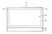
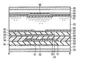
- FIG. 3 is a plan view of the liquid crystal display device 12 according to the present embodiment.
- FIG. 4 is a cross-sectional view of the liquid crystal display device 12 according to the present embodiment.
- the liquid crystal display device 12 includes a TFT substrate 31 on which TFTs, pixel electrodes, and the like are formed, a color filter substrate (CF substrate) 32 on which color filters, common electrodes, and the like are formed and disposed opposite to the TFT substrate 31, and a TFT substrate. 31 and a liquid crystal layer 33 sandwiched between the CF substrate 32.
- Each of the TFT substrate 31 and the CF substrate 32 is composed of a transparent substrate (for example, a glass substrate).
- the TFT substrate 31 is disposed on the light source unit 11 side, and illumination light from the light source unit 11 enters the liquid crystal layer 33 from the TFT substrate 31 side.
- the main surface opposite to the light source unit 11 is the display surface of the liquid crystal display device 12.
- the liquid crystal layer 33 is composed of a liquid crystal material sealed by a sealing material 34 that bonds the TFT substrate 31 and the CF substrate 32 together.
- a region surrounded by the sealing material 34 is a display region VA of the liquid crystal display device 12.
- the alignment of liquid crystal molecules is manipulated according to the electric field applied between the TFT substrate 31 and the CF substrate 32, and the optical characteristics change.
- various liquid crystal modes such as a VA (Vertical Alignment) mode, a TN (Twisted Nematic) mode, and a homogeneous mode can be used.
- the sealing material 34 is made of, for example, an ultraviolet curable resin, a thermosetting resin, or an ultraviolet / heat combination type curable resin, and is applied to the TFT substrate 31 or the CF substrate 32 in the manufacturing process, and then irradiated with ultraviolet rays or heated. Cured.
- a conduction terminal 37 is provided for conducting between the two substrates. With this conduction terminal 37, the TFT substrate 31 and the CF substrate 32 can be electrically connected.
- the circularly polarizing plates 35 and 36 are provided so as to sandwich the TFT substrate 31 and the CF substrate 32.
- Each of the circularly polarizing plates 35 and 36 includes a retardation plate (1 ⁇ 4 wavelength plate) and a polarizing plate (linear polarizer).
- the polarizing plate has a transmission axis and an absorption axis orthogonal to each other in a plane orthogonal to the light traveling direction.
- the polarizing plate transmits linearly polarized light having a vibrating surface parallel to the transmission axis (linearly polarized light component) out of light having a vibrating surface in a random direction and having a vibrating surface parallel to the absorption axis ( Absorbs linearly polarized light components).
- the two polarizing plates are arranged so that their transmission axes are orthogonal to each other, that is, in an orthogonal Nicol state.
- the retardation plate has refractive index anisotropy, and has a slow axis and a fast axis that are orthogonal to each other in a plane that is orthogonal to the traveling direction of light.
- the retardation plate has a function of giving a predetermined retardation (a phase difference of ⁇ / 4 when ⁇ is a wavelength of light transmitted) between light of a predetermined wavelength that transmits the slow axis and the fast axis.
- the slow axis of the retardation plate is set to make an angle of approximately 45 ° with respect to the transmission axis of the polarizing plate.
- regulates the polarizing plate and phase difference plate mentioned above shall contain the error which can implement
- the above approximate 45 ° includes a range of 45 ° ⁇ 5 °.
- the orthogonality mentioned above includes a range of 90 ° ⁇ 5 °.
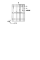
- FIG. 5 is a schematic diagram of the display area VA of the liquid crystal display device 12.
- a plurality of scanning lines GL each extending in the row direction (X direction) and a plurality of signal lines SL each extending in the column direction (Y direction) are arranged.
- a region surrounded by two adjacent scanning lines GL and two adjacent signal lines SL is a pixel region.
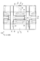
- FIG. 6 is a circuit diagram of the pixel array.
- the liquid crystal display device 12 includes a pixel array in which a plurality of pixels 40 are arranged in a matrix. In FIG. 6, four pixels 40 are extracted and shown.
- the pixel 40 includes a switching element 41, a liquid crystal capacitor (liquid crystal element) Clc, and a storage capacitor Cs.
- a switching element 41 for example, a TFT (Thin-Film-Transistor) is used, and an n-channel TFT is used.
- the source of the TFT 41 is electrically connected to the signal line SL.
- the gate of the TFT 41 is electrically connected to the scanning line GL.
- the drain of the TFT 41 is electrically connected to the liquid crystal capacitor Clc.
- the liquid crystal capacitance Clc as a liquid crystal element is composed of a pixel electrode, a common electrode, and a liquid crystal layer sandwiched between them.
- the storage capacitor Cs is connected in parallel to the liquid crystal capacitor Clc.
- the storage capacitor Cs has a function of suppressing the potential fluctuation generated in the pixel electrode and holding the drive voltage applied to the pixel electrode until the drive voltage corresponding to the next signal is applied.
- the storage capacitor Cs includes a pixel electrode, a storage electrode, and an insulating layer sandwiched between them. A common voltage Vcom is applied to the common electrode and the storage electrode.
- the liquid crystal display device 12 includes a scanning driver 42, a signal driver 43, a common voltage supply circuit 44, and the like.
- the scanning driver 42 is connected to a plurality of scanning lines GL. Based on a vertical control signal sent from a control circuit (not shown), the scan driver 42 sends a scan signal for turning on / off switching elements included in the pixel to the pixel array.
- the signal driver 43 is connected to a plurality of signal lines SL.
- the signal driver 43 receives a horizontal control signal and image data from the control circuit.
- the signal driver 43 sends a gradation signal (drive voltage) corresponding to the image data to the pixel array based on the horizontal control signal.
- the common voltage supply circuit 44 generates a common voltage Vcom and supplies it to the pixel array.
- inversion driving AC driving
- the polarity of the electric field between the pixel electrode and the common electrode sandwiching the liquid crystal is inverted at a predetermined period.
- the polarities of the common voltage Vcom and the drive voltage are inverted every predetermined period.
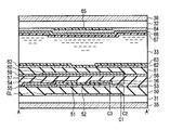
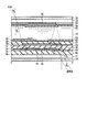
- FIG. 7 is a plan view of the liquid crystal display device 12 according to the first embodiment.
- FIG. 8 is a cross-sectional view of the liquid crystal display device 12 taken along line AA ′ of FIG.
- FIG. 9 is a cross-sectional view of the liquid crystal display device 12 taken along line BB ′ of FIG.
- FIG. 7 is a plan view in which the TFT 41 and its periphery are extracted.
- the TFT 41 is disposed between two adjacent source lines SL and on the scanning line GL.
- a scanning line GL functioning as a gate electrode of the TFT 41 is provided on the liquid crystal layer 33 side of the TFT substrate 31.
- the scanning line may be referred to as a gate electrode.
- An insulating layer 50 that functions as a gate insulating film of the TFT 41 is provided on the gate electrode GL.
- a semiconductor layer (for example, an amorphous silicon layer) 51 is provided on the insulating layer 50.
- a protective film 52 is partially provided on the semiconductor layer 51.
- the protective film 52 has a function of protecting the semiconductor layer 51 when an electrode formed on the semiconductor layer 51 is processed.
- the protective film 52 extends from the center of the semiconductor layer 51 to both sides in the X direction, and is formed so as to cover an interval between a source electrode and a drain electrode described later.
- a source electrode 53 and a drain electrode 54 are provided on the semiconductor layer 51 and the protective film 52 so as to be separated from each other in the Y direction.
- the source electrode 53 and the drain electrode 54 are provided in contact with the semiconductor layer 51.
- the gate electrode GL, the gate insulating film (insulating layer 50), the semiconductor layer 51, the source electrode 53, and the drain electrode 54 constitute the TFT 41.
- connection electrode 56 for electrically connecting the source electrode 53 and the source line SL is provided on the insulating layer 50 so as to extend in the Y direction.
- connection electrode 55 extending from the drain electrode 54 in the Y direction is provided.
- a connection electrode 57 extending in the Y direction is provided on the drain electrode 54 and the connection electrode 55.
- the connection electrode 55 and the connection electrode 57 are for electrically connecting the drain electrode 54 and the pixel electrode, and the connection electrode 57 is electrically connected to the pixel electrode via a contact (not shown).
- An insulating layer 58 is provided on the TFT 41 and various electrodes connected thereto.
- a storage electrode 59 constituting the storage capacitor Cs is provided on the insulating layer 58.
- the storage electrode 59 is formed so as to at least partially overlap the pixel electrode in plan view. From the viewpoint of suppressing an unnecessary electric field from being applied to the liquid crystal layer due to a voltage for operating the TFT 41, the storage electrode 59 to which the common voltage Vcom is applied is formed so as to cover the TFT 41. desirable.
- the storage electrode 59 is formed in a planar shape over the entire display area VA, and a plurality of openings (not shown) for passing through contacts that electrically connect the pixel electrode and the drain electrode. Is formed. That is, the storage electrode 59 is formed on the entire surface in the region extracted in the plan view of FIG.
- the portion of the storage electrode 59 that overlaps the pixel electrode constitutes a storage capacitor Cs together with the pixel electrode.
- a portion of the storage electrode 59 that overlaps with the gate electrode, the source electrode, and the drain electrode has a function of suppressing capacitive coupling of the gate electrode, the source electrode, and the drain electrode with the pixel electrode.
- a light shielding film 60 for shielding the TFT 41 is provided on the storage electrode 59.
- the light shielding film 60 is formed so as to extend in the X direction along the gate electrode GL.
- the width of the light shielding film 60 (the length in the Y direction) is wider than the width of the gate electrode GL. Accordingly, the light shielding film 60 can cover the TFT 41 (gate electrode GL, semiconductor layer 51, source electrode 53, and drain electrode 54).
- An insulating layer 61 is provided on the storage electrode 59 and the light shielding film 60.
- a pixel electrode 62 is provided corresponding to each pixel.
- the pixel electrode 62 has substantially the same planar shape as the pixel region in FIG. As described above, the pixel electrode 62 is electrically connected to the connection electrode 57 via the contact.
- An alignment film 63 is provided on the pixel electrode 62.
- the alignment film 63 controls the alignment of the liquid crystal layer 33.
- a color filter 64 is provided on the liquid crystal layer 33 side of the CF substrate 32.
- the color filter 64 includes a plurality of coloring filters (coloring members), and specifically includes a plurality of red filters, a plurality of green filters, and a plurality of blue filters.
- a general color filter is composed of three primary colors of light, red (R), green (G), and blue (B).
- a set of three colors R, G, and B adjacent to each other is a display unit (pixel), and any single color portion of R, G, B in one pixel is a minimum called a subpixel (subpixel). It is a drive unit.
- the TFT 41 and the pixel electrode 62 are provided for each subpixel. In the following description, a subpixel is referred to as a pixel unless it is particularly necessary to distinguish between a pixel and a subpixel.
- a black mask (light shielding film, black matrix) 65 for light shielding is provided on the CF substrate 32 and at the boundary between pixel regions adjacent to each other in the X direction and the Y direction.
- the black mask 65 is formed in a mesh shape so as to substantially cover the area other than the pixel area of FIG.
- the black mask 65 has a function of shielding unnecessary light between the coloring members and improving contrast.
- a common electrode 66 is provided on the color filter 64.
- the common electrode 66 is formed in a planar shape over the entire display area VA.
- An alignment film 67 is provided on the common electrode 66. The alignment film 67 controls the alignment of the liquid crystal layer 33.
- connection electrode 56, the connection electrode 57, the storage electrode 59, the pixel electrode 62, and the common electrode 66 are made of transparent electrodes, for example, ITO (indium tin oxide).
- ITO indium tin oxide
- a transparent insulating material is used, for example, silicon nitride (SiN).
- a conductive material is used, and for example, chromium (Cr), molybdenum (Mo), an alloy containing one or more of these, or chromium oxide is used.
- the black mask 65 a laminated film in which chromium oxide and chromium (Cr) are sequentially laminated, a black resin, or the like is used.
- the source electrode 53, the drain electrode 54, the connection electrode 55, the gate electrode GL, and the signal line SL for example, any of aluminum (Al), molybdenum (Mo), chromium (Cr), and tungsten (W), or An alloy containing one or more of these is used.
- the source electrode 53, the drain electrode 54, the connection electrode 55, the gate electrode GL, and the signal line SL are preferably formed using a conductive material having a large optical density (OD).
- the light shielding film 60 covers the TFT 41.
- the width of the light shielding film 60 (the length in the Y direction) is wider than the width of the gate electrode GL. Further, the distance from the end of the source electrode 53 to the end of the drain electrode 54 is shorter than the width of the light shielding film 60.
- the centers of the gate electrode GL, the light shielding film 60, the semiconductor layer 51, the protective film 52, and the black mask 65 in the Y direction are set to be the same. Actually, an error during the manufacturing process occurs in the positional relationship, and a difference due to this error is included in this embodiment.
- FIG 8 and 9 illustrate a perpendicular C1 passing through the end of the gate electrode GL, a perpendicular C2 passing through the end of the light shielding film 60, and a perpendicular C3 passing through the end of the source electrode 53.
- the perpendicular line C1 is disposed inside the perpendicular line C2.
- the perpendicular line C3 is disposed inside the perpendicular lines C1 and C2.
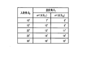
- the illumination light from the light source unit 11 is incident on the liquid crystal display device 12 from the TFT substrate 31 side at an incident angle ⁇ 0 .
- the refraction angle ⁇ 1 of the liquid crystal display device 12 is assumed.
- the illumination light reflected by the black mask 65 is shielded by the light shielding film 60 and is not incident on the TFT 41 (particularly the semiconductor layer 51). Further, the illumination light reflected by the light shielding film 60 is hardly incident on the semiconductor layer 51 because it is repeatedly reflected and attenuated.
- External light enters the liquid crystal display device 12 from the CF substrate 32 side at an incident angle ⁇ 0 . Since the external light reflected by the connection electrode 55 is repeatedly reflected and attenuated, it hardly enters the semiconductor layer 51. Further, as shown in FIG. 11, the external light reflected by the gate electrode GL hardly attenuates incident on the semiconductor layer 51 because it is repeatedly reflected and attenuated.
- the light intensity incident on the TFT 41 can be reduced.
- the light leakage current of the TFT 41 can be reduced.
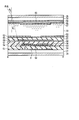
- FIG. 12 is a plan view of the liquid crystal display device 12 according to the second embodiment.
- FIG. 13 is a cross-sectional view of the liquid crystal display device 12 taken along line AA ′ of FIG.
- FIG. 14 is a cross-sectional view of the liquid crystal display device 12 taken along line BB ′ of FIG.
- the width of the light shielding film 60 is narrower than the width of the gate electrode GL.
- the length between both ends of the source electrode 53 and the drain electrode 54 is narrower than the width of the gate electrode GL.
- the width of the black mask 65 is narrower than the width of the gate electrode GL.
- FIG. 13 and 14 illustrate a perpendicular line C1 passing through the end of the gate electrode GL, a perpendicular line C2 passing through the end of the light shielding film 60, and a perpendicular line C3 passing through the end of the source electrode 53.
- the perpendicular line C2 is disposed inside the perpendicular line C1.
- the perpendicular line C3 is disposed inside the perpendicular lines C1 and C2.
- the illumination light from the light source unit 11 enters the liquid crystal display device 12 from the TFT substrate 31 side at an incident angle ⁇ 0 .
- the refraction angle ⁇ 1 of the liquid crystal display device 12 is assumed.
- the illumination light passing near the end of the gate electrode GL is not reflected by the light shielding film 60. Thereby, the illumination light which injects into TFT41 (especially semiconductor layer 51) can be reduced more.
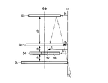
- FIG. 16 is a schematic diagram for explaining the conditions of the light shielding film 60, the source electrode 53, and the black mask 65.
- a distance d 1 is a distance between the gate electrode GL and the source electrode 53.
- the distance d 1 is the total thickness of the insulating layer 50 and the semiconductor layer 51. Since the thickness of the insulating layer 50 is sufficiently larger than the thickness of the semiconductor layer 51, the distance d 1 can thickness and approximation of the insulating layer 50 (thickness d 1 ⁇ insulating layer 50).
- the distance d 2 is a distance between the source electrode 53 and the light shielding film 60.
- the distance d 2 is the total thickness of the insulating layer 58 and the storage electrode 59. Since the thickness of the insulating layer 58 is sufficiently thicker than the thickness of the storage electrode 59, the distance d 2 can be approximated to the thickness of the insulating layer 58 (d 2 ⁇ thickness of the insulating layer 58).
- the distance d 3 is a distance between the light shielding film 60 and the black mask 65.
- the distance d 3 an insulating layer 61, pixel electrodes 62, an alignment film 63, the liquid crystal layer 33, orientation film 67, common electrode 66, and the sum of the thickness of the color filter 64.
- each of the insulating layer 61, the liquid crystal layer 33, and the color filter 64 is sufficiently thicker than the thickness of each of the pixel electrode 62, the common electrode 66, and the alignment films 63 and 67, the distance d 3 is equal to the insulating layer 61, The total thickness of the liquid crystal layer 33 and the color filter 64 can be approximated (d 2 ⁇ “thickness of the insulating layer 61” + “thickness of the liquid crystal layer 33” + “thickness of the color filter 64”).
- the distances S 1 , S 2 , and S 3 are defined based on the perpendicular line C1 passing through the end of the gate electrode GL.
- the distance S 1 is a distance from the perpendicular line C 1 to the source electrode 53.
- the distance S 2 is the distance from the perpendicular line C1 to the light-shielding film 60.
- the distance S 3 is the distance from the perpendicular line C1 to the black mask 65.
- the refractive indexes of the circularly polarizing plate, the glass substrate, the alignment film, the color filter, the liquid crystal layer, and the semiconductor layer (amorphous silicon) are substantially the same and are approximately 1.5.
- the refractive indexes of the transparent electrode (ITO) and the insulating layer (silicon nitride) are approximately the same, approximately 1.8.
- Transparent electrode (ITO) and the refractive angle theta 12 of the insulating layer (silicon nitride). Incident angle ⁇ 0 .
- the distance S 1 satisfies the condition that illumination light that is not shielded by the gate electrode GL is not reflected by the source electrode 53. Thereby, the illumination light reflected by the source electrode 53 can be prevented from entering the semiconductor layer 51. That is, the distance S 1 satisfies the following conditions of Equation (1). S 1 > d 1 ⁇ tan ⁇ 12 (1)
- the distance S 2 satisfies the condition that the illumination light is not shielded by the gate electrode GL is not reflected by the light shielding film 60. Thereby, the illumination light reflected by the light shielding film 60 can be prevented from entering the semiconductor layer 51. That is, the distance S 2 satisfies the following conditions of Equation (2). S 2 > (d 1 + d 2 ) ⁇ tan ⁇ 12 (2)
- the distance S 3 is greater than 0. That is, the end of the black mask 65 is disposed on the inner side (center side of the gate electrode GL) than the end of the gate electrode GL. In other words, the width of the black mask 65 is narrower than the width of the gate electrode GL. Thereby, it can prevent that an aperture ratio falls. Considering a margin for misalignment during the manufacturing process of bonding the TFT substrate 31 and the CF substrate 32, the distance S 3 is preferably larger than the distance S 2.
- the distance S 4 from the perpendicular C1 to end inside the source electrode 53 (the drain electrode 54 side), the distance S 1, S 2, S 3, respectively, the distance S 4 less.
- the distances S 2 and S 3 are equal to or longer than the distance S 4 , light enters the semiconductor layer 51 from the upper side of the drawing.
- the drain electrode 54 is also configured under the same conditions as the source electrode 53 with respect to the light shielding film 60, the gate electrode GL, and the black mask 65. Therefore, even in a configuration in which illumination light is incident obliquely from the drain electrode 54 side, the same operation and effect as in the case of the source electrode 53 can be obtained.
- the head-up display device 10 includes the liquid crystal display device 12, and the liquid crystal display device 12 receives illumination light from the light source unit 11 from an oblique direction.
- the liquid crystal display device 12 includes a storage electrode 59 provided above the switching element (TFT) 41 via an insulating layer 58 and a light shielding film 60 provided on the storage electrode 59.
- the present embodiment it is possible to prevent light from above the switching element 41 (CF substrate 32 side) from entering the switching element 41 (particularly, the semiconductor layer 51). Thereby, since the light leakage current can be reduced by the switching element, the image quality of the liquid crystal display device 12 can be improved.
- the width of the light shielding film 60 (the length in the Y direction) is set to be narrower than the width of the gate electrode GL. Thereby, the light reflected by the light shielding film 60 can be prevented from entering the semiconductor layer 51.
- the length between both ends of the source electrode 53 and the drain electrode 54 is set to be narrower than the width of the gate electrode GL. Thereby, it is possible to suppress the light reflected by the source electrode 53 and the drain electrode 54 from entering the semiconductor layer 51.
- a black mask 65 is provided on the CF substrate 32, and the width of the black mask 65 is set to be narrower than the width of the gate electrode GL. Thereby, it can prevent that an aperture ratio (transmittance) falls.
- the light shielding film 60 is made of a conductive material and is electrically connected to the storage electrode 59. That is, the light shielding film 60 is set to the same voltage (common voltage Vcom) as the storage electrode 59. Thereby, it is possible to suppress an unnecessary electric field from being applied to the liquid crystal layer 33 due to the light shielding film 60.
- a plate or a film is an expression illustrating the member, and is not limited to the configuration.
- the retardation plate is not limited to a plate-like member, and may be a film having other functions described in the specification or other members.
- the polarizing plate is not limited to a plate-like member, and may be a film having other functions described in the specification or other members.
- the present invention is not limited to the embodiment described above, and can be embodied by modifying the constituent elements without departing from the scope of the invention. Further, the above embodiments include inventions at various stages, and are obtained by appropriately combining a plurality of constituent elements disclosed in one embodiment or by appropriately combining constituent elements disclosed in different embodiments. Various inventions can be configured. For example, even if some constituent elements are deleted from all the constituent elements disclosed in the embodiments, the problems to be solved by the invention can be solved and the effects of the invention can be obtained. Embodiments made can be extracted as inventions.
Landscapes
- Physics & Mathematics (AREA)
- Nonlinear Science (AREA)
- General Physics & Mathematics (AREA)
- Optics & Photonics (AREA)
- Chemical & Material Sciences (AREA)
- Engineering & Computer Science (AREA)
- Mathematical Physics (AREA)
- Crystallography & Structural Chemistry (AREA)
- Microelectronics & Electronic Packaging (AREA)
- Liquid Crystal (AREA)
- Combustion & Propulsion (AREA)
- Transportation (AREA)
- Mechanical Engineering (AREA)
Abstract
On décrit un dispositif d'affichage à cristaux liquides qui comprend: un premier et un second substrat (31, 32) disposés de manière à recevoir, à partir de la direction diagonale, de la lumière provenant d'une source de lumière, lesdits premier et second substrat étant disposés l'un en face de l'autre; une couche de cristaux liquides (33) prise en sandwich entre le premier et le second substrat (31, 32); un élément de commutation (41) disposé sur le premier substrat (31) et muni d'une électrode de grille; un film de blocage de lumière (60) placé au-dessus de l'élément de commutation (41) par l'intermédiaire d'une couche isolante (58); une électrode de pixel (62) placée au-dessus du film de blocage de lumière (60) par l'intermédiaire d'une couche isolante (61); et un film de blocage de lumière (65) disposé sur le second substrat (32), ledit film de blocage de lumière étant placé dans des zones périphériques situées entre des pixels adjacents les uns aux autres, et au-dessus de l'élément de commutation (41).
Priority Applications (4)
| Application Number | Priority Date | Filing Date | Title |
|---|---|---|---|
| KR1020177032863A KR102105748B1 (ko) | 2015-05-11 | 2016-04-22 | 액정 표시 장치 및 헤드업 디스플레이 장치 |
| EP16792521.3A EP3296812B1 (fr) | 2015-05-11 | 2016-04-22 | Dispositif d'affichage à cristaux liquides et dispositif d'affichage tête haute |
| CN201680027154.7A CN107615154B (zh) | 2015-05-11 | 2016-04-22 | 液晶显示装置及平视显示器装置 |
| US15/800,714 US10345584B2 (en) | 2015-05-11 | 2017-11-01 | Liquid crystal display and head-up display device |
Applications Claiming Priority (2)
| Application Number | Priority Date | Filing Date | Title |
|---|---|---|---|
| JP2015096676A JP6550912B2 (ja) | 2015-05-11 | 2015-05-11 | 液晶表示装置及びヘッドアップディスプレイ装置 |
| JP2015-096676 | 2015-05-11 |
Related Child Applications (1)
| Application Number | Title | Priority Date | Filing Date |
|---|---|---|---|
| US15/800,714 Continuation US10345584B2 (en) | 2015-05-11 | 2017-11-01 | Liquid crystal display and head-up display device |
Publications (1)
| Publication Number | Publication Date |
|---|---|
| WO2016181796A1 true WO2016181796A1 (fr) | 2016-11-17 |
Family
ID=57248972
Family Applications (1)
| Application Number | Title | Priority Date | Filing Date |
|---|---|---|---|
| PCT/JP2016/062805 WO2016181796A1 (fr) | 2015-05-11 | 2016-04-22 | Dispositif d'affichage à cristaux liquides et dispositif d'affichage tête haute |
Country Status (7)
| Country | Link |
|---|---|
| US (1) | US10345584B2 (fr) |
| EP (1) | EP3296812B1 (fr) |
| JP (1) | JP6550912B2 (fr) |
| KR (1) | KR102105748B1 (fr) |
| CN (1) | CN107615154B (fr) |
| TW (1) | TWI594045B (fr) |
| WO (1) | WO2016181796A1 (fr) |
Cited By (1)
| Publication number | Priority date | Publication date | Assignee | Title |
|---|---|---|---|---|
| US10620433B2 (en) | 2018-01-19 | 2020-04-14 | Toppan Printing Co., Ltd. | Head-up display device |
Families Citing this family (7)
| Publication number | Priority date | Publication date | Assignee | Title |
|---|---|---|---|---|
| JP2019086766A (ja) | 2017-11-09 | 2019-06-06 | 日東電工株式会社 | ヘッドアップディスプレイ装置 |
| CN108681165B (zh) * | 2018-03-29 | 2021-04-02 | 厦门天马微电子有限公司 | 显示装置 |
| JP2020134588A (ja) * | 2019-02-14 | 2020-08-31 | 株式会社デンソー | 虚像表示装置 |
| JP7304573B2 (ja) * | 2019-07-26 | 2023-07-07 | パナソニックIpマネジメント株式会社 | ヘッドアップディスプレイ装置 |
| TWI826508B (zh) * | 2019-08-23 | 2023-12-21 | 揚明光學股份有限公司 | 投影模組及包括該投影模組的交通工具 |
| WO2021193074A1 (fr) * | 2020-03-26 | 2021-09-30 | 株式会社小糸製作所 | Dispositif de génération d'images, miroir réfléchissant et dispositif d'affichage tête haute |
| JP2022142922A (ja) * | 2021-03-17 | 2022-10-03 | セイコーエプソン株式会社 | 電気光学装置、および電子機器 |
Citations (4)
| Publication number | Priority date | Publication date | Assignee | Title |
|---|---|---|---|---|
| JP2001305580A (ja) * | 2000-04-24 | 2001-10-31 | Seiko Epson Corp | 電気光学装置 |
| JP2010211065A (ja) * | 2009-03-11 | 2010-09-24 | Denso Corp | 表示装置 |
| JP2013109258A (ja) * | 2011-11-24 | 2013-06-06 | Seiko Epson Corp | 電気光学装置および電子機器 |
| JP2015079227A (ja) * | 2013-10-18 | 2015-04-23 | 株式会社 オルタステクノロジー | 液晶表示装置及びヘッドアップディスプレイ |
Family Cites Families (6)
| Publication number | Priority date | Publication date | Assignee | Title |
|---|---|---|---|---|
| JP2003172946A (ja) * | 2001-09-28 | 2003-06-20 | Fujitsu Display Technologies Corp | 液晶表示装置用基板及びそれを用いた液晶表示装置 |
| JP4419119B2 (ja) * | 2003-12-03 | 2010-02-24 | 日本電気株式会社 | 電気光学装置及び投射型表示装置 |
| JP2007171867A (ja) * | 2005-12-26 | 2007-07-05 | Seiko Epson Corp | 反射型液晶表示基板、反射型液晶表示装置、電子機器及び投射型表示装置 |
| JP4254855B2 (ja) | 2006-12-20 | 2009-04-15 | ソニー株式会社 | 液晶表示装置およびその製造方法 |
| KR101337195B1 (ko) * | 2008-10-10 | 2013-12-05 | 엘지디스플레이 주식회사 | 액정표시장치용 어레이기판 및 그의 제조방법, 이를 구비한액정표시장치 |
| CN104216188B (zh) * | 2014-09-05 | 2017-05-10 | 京东方科技集团股份有限公司 | 一种显示面板和显示装置 |
-
2015
- 2015-05-11 JP JP2015096676A patent/JP6550912B2/ja active Active
-
2016
- 2016-04-22 EP EP16792521.3A patent/EP3296812B1/fr active Active
- 2016-04-22 CN CN201680027154.7A patent/CN107615154B/zh active Active
- 2016-04-22 WO PCT/JP2016/062805 patent/WO2016181796A1/fr active Application Filing
- 2016-04-22 KR KR1020177032863A patent/KR102105748B1/ko active IP Right Grant
- 2016-05-03 TW TW105113690A patent/TWI594045B/zh active
-
2017
- 2017-11-01 US US15/800,714 patent/US10345584B2/en active Active
Patent Citations (4)
| Publication number | Priority date | Publication date | Assignee | Title |
|---|---|---|---|---|
| JP2001305580A (ja) * | 2000-04-24 | 2001-10-31 | Seiko Epson Corp | 電気光学装置 |
| JP2010211065A (ja) * | 2009-03-11 | 2010-09-24 | Denso Corp | 表示装置 |
| JP2013109258A (ja) * | 2011-11-24 | 2013-06-06 | Seiko Epson Corp | 電気光学装置および電子機器 |
| JP2015079227A (ja) * | 2013-10-18 | 2015-04-23 | 株式会社 オルタステクノロジー | 液晶表示装置及びヘッドアップディスプレイ |
Non-Patent Citations (1)
| Title |
|---|
| See also references of EP3296812A4 * |
Cited By (2)
| Publication number | Priority date | Publication date | Assignee | Title |
|---|---|---|---|---|
| US10620433B2 (en) | 2018-01-19 | 2020-04-14 | Toppan Printing Co., Ltd. | Head-up display device |
| DE102018131804B4 (de) * | 2018-01-19 | 2021-01-21 | Toppan Printing Co., Ltd. | Head-up-Display |
Also Published As
| Publication number | Publication date |
|---|---|
| TW201643512A (zh) | 2016-12-16 |
| JP6550912B2 (ja) | 2019-07-31 |
| US20180067311A1 (en) | 2018-03-08 |
| TWI594045B (zh) | 2017-08-01 |
| EP3296812A1 (fr) | 2018-03-21 |
| CN107615154A (zh) | 2018-01-19 |
| EP3296812B1 (fr) | 2022-01-05 |
| KR20170137186A (ko) | 2017-12-12 |
| CN107615154B (zh) | 2021-02-09 |
| JP2016212292A (ja) | 2016-12-15 |
| EP3296812A4 (fr) | 2019-01-09 |
| US10345584B2 (en) | 2019-07-09 |
| KR102105748B1 (ko) | 2020-04-28 |
Similar Documents
| Publication | Publication Date | Title |
|---|---|---|
| JP6550912B2 (ja) | 液晶表示装置及びヘッドアップディスプレイ装置 | |
| JP6247952B2 (ja) | ヘッドアップディスプレイ装置 | |
| JP6200798B2 (ja) | 液晶表示装置及びヘッドアップディスプレイ装置 | |
| JP2015118272A (ja) | ヘッドアップディスプレイ装置用液晶表示装置及びヘッドアップディスプレイ装置 | |
| US9568771B2 (en) | Liquid crystal device, electronic device and projector with maximum-light-intensity direction inclined from the direction normal to the substrates | |
| JP2011053386A (ja) | 表示装置、電子機器、投射型映像装置 | |
| WO2015056792A1 (fr) | Dispositif d'affichage à cristaux liquides et affichage tête haute | |
| US11703724B2 (en) | Electronic device including a liquid crystal panel | |
| US11815774B2 (en) | Electronic device | |
| US11789321B2 (en) | Electronic device | |
| JP7150627B2 (ja) | 電子機器 | |
| US20220155644A1 (en) | Electronic device | |
| JP6531313B2 (ja) | 液晶表示装置 | |
| JP7073735B2 (ja) | ヘッドアップディスプレイ装置 | |
| US11874566B2 (en) | Electronic device | |
| US11703730B2 (en) | Electronic device | |
| JP6859703B2 (ja) | 液晶表示装置 |
Legal Events
| Date | Code | Title | Description |
|---|---|---|---|
| 121 | Ep: the epo has been informed by wipo that ep was designated in this application |
Ref document number: 16792521 Country of ref document: EP Kind code of ref document: A1 |
|
| ENP | Entry into the national phase |
Ref document number: 20177032863 Country of ref document: KR Kind code of ref document: A |
|
| NENP | Non-entry into the national phase |
Ref country code: DE |
|
| WWE | Wipo information: entry into national phase |
Ref document number: 2016792521 Country of ref document: EP |