WO2016174892A1 - Ledパッケージ、発光装置およびledパッケージの製造方法 - Google Patents
Ledパッケージ、発光装置およびledパッケージの製造方法 Download PDFInfo
- Publication number
- WO2016174892A1 WO2016174892A1 PCT/JP2016/053835 JP2016053835W WO2016174892A1 WO 2016174892 A1 WO2016174892 A1 WO 2016174892A1 JP 2016053835 W JP2016053835 W JP 2016053835W WO 2016174892 A1 WO2016174892 A1 WO 2016174892A1
- Authority
- WO
- WIPO (PCT)
- Prior art keywords
- led
- electrode
- auxiliary electrode
- led package
- phosphor layer
- Prior art date
- Legal status (The legal status is an assumption and is not a legal conclusion. Google has not performed a legal analysis and makes no representation as to the accuracy of the status listed.)
- Ceased
Links
Images





Classifications
-
- H—ELECTRICITY
- H10—SEMICONDUCTOR DEVICES; ELECTRIC SOLID-STATE DEVICES NOT OTHERWISE PROVIDED FOR
- H10H—INORGANIC LIGHT-EMITTING SEMICONDUCTOR DEVICES HAVING POTENTIAL BARRIERS
- H10H20/00—Individual inorganic light-emitting semiconductor devices having potential barriers, e.g. light-emitting diodes [LED]
- H10H20/80—Constructional details
- H10H20/85—Packages
- H10H20/857—Interconnections, e.g. lead-frames, bond wires or solder balls
-
- H—ELECTRICITY
- H10—SEMICONDUCTOR DEVICES; ELECTRIC SOLID-STATE DEVICES NOT OTHERWISE PROVIDED FOR
- H10H—INORGANIC LIGHT-EMITTING SEMICONDUCTOR DEVICES HAVING POTENTIAL BARRIERS
- H10H20/00—Individual inorganic light-emitting semiconductor devices having potential barriers, e.g. light-emitting diodes [LED]
- H10H20/80—Constructional details
- H10H20/83—Electrodes
- H10H20/831—Electrodes characterised by their shape
-
- H—ELECTRICITY
- H10—SEMICONDUCTOR DEVICES; ELECTRIC SOLID-STATE DEVICES NOT OTHERWISE PROVIDED FOR
- H10H—INORGANIC LIGHT-EMITTING SEMICONDUCTOR DEVICES HAVING POTENTIAL BARRIERS
- H10H20/00—Individual inorganic light-emitting semiconductor devices having potential barriers, e.g. light-emitting diodes [LED]
- H10H20/80—Constructional details
- H10H20/84—Coatings, e.g. passivation layers or antireflective coatings
-
- H—ELECTRICITY
- H10—SEMICONDUCTOR DEVICES; ELECTRIC SOLID-STATE DEVICES NOT OTHERWISE PROVIDED FOR
- H10H—INORGANIC LIGHT-EMITTING SEMICONDUCTOR DEVICES HAVING POTENTIAL BARRIERS
- H10H20/00—Individual inorganic light-emitting semiconductor devices having potential barriers, e.g. light-emitting diodes [LED]
- H10H20/80—Constructional details
- H10H20/85—Packages
- H10H20/851—Wavelength conversion means
-
- H—ELECTRICITY
- H10—SEMICONDUCTOR DEVICES; ELECTRIC SOLID-STATE DEVICES NOT OTHERWISE PROVIDED FOR
- H10H—INORGANIC LIGHT-EMITTING SEMICONDUCTOR DEVICES HAVING POTENTIAL BARRIERS
- H10H20/00—Individual inorganic light-emitting semiconductor devices having potential barriers, e.g. light-emitting diodes [LED]
- H10H20/80—Constructional details
- H10H20/85—Packages
- H10H20/851—Wavelength conversion means
- H10H20/8514—Wavelength conversion means characterised by their shape, e.g. plate or foil
-
- H—ELECTRICITY
- H10—SEMICONDUCTOR DEVICES; ELECTRIC SOLID-STATE DEVICES NOT OTHERWISE PROVIDED FOR
- H10W—GENERIC PACKAGES, INTERCONNECTIONS, CONNECTORS OR OTHER CONSTRUCTIONAL DETAILS OF DEVICES COVERED BY CLASS H10
- H10W72/00—Interconnections or connectors in packages
-
- H—ELECTRICITY
- H10—SEMICONDUCTOR DEVICES; ELECTRIC SOLID-STATE DEVICES NOT OTHERWISE PROVIDED FOR
- H10H—INORGANIC LIGHT-EMITTING SEMICONDUCTOR DEVICES HAVING POTENTIAL BARRIERS
- H10H20/00—Individual inorganic light-emitting semiconductor devices having potential barriers, e.g. light-emitting diodes [LED]
- H10H20/01—Manufacture or treatment
- H10H20/032—Manufacture or treatment of electrodes
-
- H—ELECTRICITY
- H10—SEMICONDUCTOR DEVICES; ELECTRIC SOLID-STATE DEVICES NOT OTHERWISE PROVIDED FOR
- H10H—INORGANIC LIGHT-EMITTING SEMICONDUCTOR DEVICES HAVING POTENTIAL BARRIERS
- H10H20/00—Individual inorganic light-emitting semiconductor devices having potential barriers, e.g. light-emitting diodes [LED]
- H10H20/01—Manufacture or treatment
- H10H20/036—Manufacture or treatment of packages
- H10H20/0364—Manufacture or treatment of packages of interconnections
-
- H—ELECTRICITY
- H10—SEMICONDUCTOR DEVICES; ELECTRIC SOLID-STATE DEVICES NOT OTHERWISE PROVIDED FOR
- H10W—GENERIC PACKAGES, INTERCONNECTIONS, CONNECTORS OR OTHER CONSTRUCTIONAL DETAILS OF DEVICES COVERED BY CLASS H10
- H10W90/00—Package configurations
- H10W90/701—Package configurations characterised by the relative positions of pads or connectors relative to package parts
- H10W90/721—Package configurations characterised by the relative positions of pads or connectors relative to package parts of bump connectors
- H10W90/726—Package configurations characterised by the relative positions of pads or connectors relative to package parts of bump connectors between a chip and a stacked lead frame, conducting package substrate or heat sink
Definitions
- the present invention relates to an LED package, a light emitting device, and an LED package manufacturing method.
- a method for mounting a semiconductor chip for example, there is known a method in which a semiconductor chip is connected to an electrode of a substrate through bump-shaped bump electrodes made of gold or solder.
- a semiconductor module has been proposed in which the shape of the bump electrode and the electrode on the substrate side is devised so that positional displacement between the two does not occur during mounting.
- Patent Literature 1 includes a semiconductor bare chip provided with bumps on the mounting surface side and a mounting board provided with connection electrodes connected to the bumps of the semiconductor bare chip. There is described a semiconductor mounting module in which a recess for guiding a protruding bump of a semiconductor bare chip is provided on the connection electrode itself or on the connection electrode.
- a protruding electrode is formed on the semiconductor chip side, an electrode having an insertion opening is formed on the substrate side, and the electrode on the semiconductor chip side is at the opening edge of the insertion opening of the substrate side electrode.
- a light emitting device having an LED (light emitting diode) package as a semiconductor chip, it is required to mount the LED package on a substrate at a high density in order to achieve high luminance.
- the deviation is automatically repaired during reflow by a phenomenon called self-alignment as long as it is within an allowable range.
- the electrodes are particularly small compared to the package body and are formed near the center of the lower surface of the package, so that self-alignment is unlikely to occur and misalignment during mounting is difficult to repair.
- an object of the present invention is to improve the mounting density of the LED package while providing the LED package used in the light emitting device with a function of position correction at the time of mounting by self-alignment.
- An LED element having an element electrode on the lower surface, a phosphor layer containing a phosphor and covering the upper surface and side surfaces of the LED element, and an auxiliary electrode whose upper surface is bonded to the lower surface of the element electrode, It has a step that is larger than the device electrode and smaller on the lower surface than the upper surface, and is arranged so that the end portion on the side where the step is formed is located inside the outer peripheral surface of the phosphor layer.
- a featured LED package is provided.
- the LED element preferably has a box shape, and the step of the auxiliary electrode is preferably formed in both the vertical and horizontal directions of the box.
- the LED element having the element electrode on the lower surface, the phosphor layer containing the phosphor and covering the upper surface and the side surface of the LED element, the auxiliary electrode whose upper surface is bonded to the lower surface of the element electrode, and the auxiliary electrode are connected.
- the auxiliary electrode has a step larger than the element electrode and smaller on the lower surface than the upper surface, and the end on the side where the step is formed is a phosphor.
- a light-emitting device is provided that is disposed so as to be located on the inner side of the outer peripheral surface of the layer.
- the LED element has two element electrodes on the lower surface, the auxiliary electrode is provided corresponding to each of the two element electrodes, and the wiring pattern of the mounting substrate is formed on the two element electrodes. It is divided into two parts to be connected to each other, and the distance between the element electrodes, the distance between the auxiliary electrodes, and the distance between the wiring patterns are preferably matched.
- a metal piece having a larger upper surface than the element electrode formed on the lower surface of the LED element and a step smaller on the lower surface than the upper surface is disposed on the substrate on which the concave portion having the same shape as the metal piece is formed.
- the step of vibrating the substrate to house the metal piece in the recess, and the phosphor layer containing the phosphor is coated on the top and side surfaces, and the width including the phosphor layer is larger than the width of the metal piece.
- a step of mounting the LED element on the metal piece accommodated in the recess so that the metal piece is connected to the element electrode of the LED element as an auxiliary electrode, and a step of removing the LED element to which the auxiliary electrode is connected from the substrate A method for manufacturing an LED package is provided.
- a plurality of metal pieces are arranged on a substrate on which a plurality of concave portions are formed, and in the mounting step, a plurality of LED elements are arranged on the plurality of metal pieces accommodated in the concave portions. It is preferable to implement.
- the LED package used in the light emitting device is provided with a function of position correction at the time of mounting by self-alignment, and the mounting density of the LED package can be improved.
- FIG. 2 is a top view of the light emitting device 1.
- FIG. It is sectional drawing of the light-emitting device 1 along the II-II line
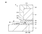
- wire of FIG. 2 is an enlarged cross-sectional view of the light emitting device 1.
- FIG. (A)-(G) are figures which show the shape of the LED element 21.
- FIG. (A)-(G) are figures which show the shape of the LED element 21 with the fluorescent substance layer 23 attached.
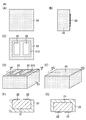
- (A)-(G) are figures which show the shape of the LED package 2 to which the auxiliary electrode 24 is further attached. It is a perspective view which shows the shape of auxiliary electrode 24 '.
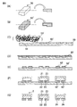
- (A) to (G) are diagrams for explaining a manufacturing process of the LED package 2.
- FIG. 1 is a top view of the light emitting device 1.
- the light emitting device 1 corresponds to a light emitting unit in various lighting devices such as lighting LEDs and LED bulbs, and includes a plurality of LED packages 2 and a mounting substrate 3 as main components.
- the plurality of LED packages 2 are densely mounted on the mounting substrate 3 (at a narrow pitch).
- FIG. 1 shows an example in which nine LED packages 2 are mounted in a 3 ⁇ 3 lattice pattern.
- FIG. 2 is a cross-sectional view of the light emitting device 1 taken along the line II-II in FIG.
- FIG. 3 is an enlarged cross-sectional view of the light emitting device 1.
- FIG. 2 shows a cross section of three of the nine LED packages 2 included in the light emitting device 1 and the mounting substrate 3.
- FIG. 3 is an enlarged view of the left end portion in FIG.
- the LED package 2 includes an LED element 21 with an element electrode 22, a phosphor layer 23, and an auxiliary electrode 24.
- the LED package 2 is a bump type light emitting element in which an auxiliary electrode 24 that is a bump for flip chip bonding is formed on the element electrode 22 on the lower surface of the LED element 21.
- an auxiliary electrode 24 that is a bump for flip chip bonding is formed on the element electrode 22 on the lower surface of the LED element 21.
- FIG. 4 (A) to 4 (G) are diagrams showing the shape of the LED element 21.
- FIG. 4A, 4B, and 4C are a top view, a side view, and a bottom view of the LED element 21, respectively.
- FIG. 4D is a perspective view of the LED element 21 with the lower surface 213 facing up (that is, upside down), and
- FIG. 4E shows the LED element 21 with the upper surface 211 facing up. It is a perspective view.
- 4F is a cross-sectional view of the LED element 21 taken along the line IVF-IVF in FIG. 4D
- FIG. 4G is a cross-sectional view taken along the line IVG-IVG in FIG.
- the LED element 21 is, for example, a blue semiconductor light emitting element (blue LED) that emits blue light having an emission wavelength band of about 450 to 460 nm.
- the LED element 21 has two (one pair) rectangular element electrodes 22 at symmetrical positions across the center of the lower surface 213.
- the illustrated LED element 21 has a rectangular parallelepiped (box shape) shape, the LED element may have another shape such as a cylinder or an octagonal prism.
- FIGS. 5A, 5B, and 5C are a top view, a side view, and a bottom view corresponding to FIGS. 4A, 4B, and 4C, respectively.
- . 5D and 5E are perspective views corresponding to FIGS. 4D and 4E, respectively.
- 5F is a cross-sectional view taken along line VF-VF in FIG. 5D
- FIG. 5G is a cross-sectional view taken along line VG-VG in FIG.
- the phosphor layer 23 is configured by dispersing and mixing phosphor particles (not shown) in a colorless and transparent resin such as an epoxy resin or a silicone resin.
- the phosphor layer 23 uniformly covers the upper surface 211 and the side surface 212 of the LED element 21 (see FIGS. 4A to 4G). That is, the phosphor layer 23 covers other than the lower surface 213 on which the element electrode 22 of the LED element 21 is formed.
- the phosphor layer 23 preferably contains phosphor particles uniformly and covers each surface of the LED element 21 except the lower surface 213 with an equal thickness.
- the phosphor layer 23 contains, for example, a yellow phosphor.
- the yellow phosphor is a particulate phosphor material such as YAG (yttrium aluminum garnet) that absorbs blue light emitted from the LED element 21 and converts the wavelength into yellow light.
- the LED package 2 emits white light obtained by mixing blue light from the LED element 21 which is a blue LED and yellow light obtained by exciting the yellow phosphor.
- the phosphor layer 23 may contain a plurality of types of phosphors such as a green phosphor and a red phosphor.
- the green phosphor is a particulate phosphor material such as (BaSr) 2 SiO 4 : Eu 2+ that absorbs blue light emitted from the LED element 21 and converts the wavelength into green light.
- the red phosphor is a particulate phosphor material such as CaAlSiN 3 : Eu 2+ that absorbs blue light emitted from the LED element 21 and converts the wavelength into red light.
- the LED package 2 is obtained by mixing blue light from the LED element 21 which is a blue LED and green light and red light obtained by exciting the green phosphor and the red phosphor thereby. Emits light.
- the type of phosphor contained in the phosphor layer 23 may be changed for each LED package 2.
- the light emitting device 1 as a whole may generate light of a color according to the application by mixing the emitted light of different colors for each LED package 2.
- FIGS. 6A, 6B, and 6C are diagrams showing the shape of the LED package 2 further provided with the auxiliary electrode 24.
- FIG. FIGS. 6A, 6B, and 6C are a top view, a side view, and a bottom view corresponding to FIGS. 4A, 4B, and 4C, respectively.
- 6 (D) and 6 (E) are perspective views corresponding to FIGS. 4 (D) and 4 (E), respectively.
- 6F is a cross-sectional view taken along the line VIF-VIF in FIG. 6D
- FIG. 6G is a cross-sectional view taken along the line VIG-VIG in FIG.
- the auxiliary electrode 24 is composed of two (one pair) metal pieces corresponding to the two element electrodes 22 respectively, and functions as a soldering electrode when the LED package 2 is fixed to the mounting substrate 3.
- the upper surface 241 of the pair of auxiliary electrodes 24 is disposed on the lower surface of the corresponding element electrode 22 with a band-shaped region (gap portion 240) passing through the center of the lower surface 213 of the LED element 21 between the pair of element electrodes 22 interposed therebetween. They are attached parallel to each other. In the gap portion 240 of the pair of auxiliary electrodes 24, the lower surface 213 of the LED element 21 is exposed.
- the individual auxiliary electrodes 24 are larger than the device electrodes 22, but the area covered with the pair of auxiliary electrodes 24 when the LED package 2 is viewed from below is smaller than the entire area of the lower surface of the LED package 2. Further, the auxiliary electrode 24 is disposed such that the outermost end portion is located on the inner side of the outer peripheral surface of the phosphor layer 23. That is, when the LED package 2 is viewed from above, the end portion of the auxiliary electrode 24 does not protrude from the phosphor layer 23, and the auxiliary electrode 24 is arranged so as not to be hidden behind the phosphor layer 23.
- Each auxiliary electrode 24 has a step 243 in which the lower surface 242 is smaller than the upper surface 241.
- the step 243 is formed in parallel to the gap portion 240 sandwiched between the pair of auxiliary electrodes 24. That is, the auxiliary electrode 24 is cut in parallel to the gap between the metal pieces so that the end portions of the two plate-like metal pieces arranged in parallel are thinner than the inner end portions. It has a shape like this. Due to the step 243, the auxiliary electrode 24 is thicker by one step on the inner side facing the gap portion 240 than on the outer side, and the lower surface 242 on the side contacting the mounting substrate 3 is higher than the upper surface 241 on the LED element 21 side. Becomes smaller.
- the mounting substrate 3 is an insulating substrate such as a glass epoxy substrate, a BT resin substrate, a ceramic substrate, or a metal core substrate.
- a wiring pattern 31 to which the auxiliary electrodes 24 of the plurality of LED packages 2 are connected is formed on the upper surface of the mounting substrate 3.
- a resist 32 is formed on the upper surface of the portion of the wiring pattern 31 that is not covered with the LED package 2 except for the left end and the right end of the mounting substrate 3 in FIG.
- the wiring pattern 31 is formed in three rows corresponding to the LED packages 2 arranged in a 3 ⁇ 3 row in the horizontal direction in FIG. As shown in FIG. 2, the wiring pattern 31 in each column has a cut under the LED package 2, and a portion to which one auxiliary electrode 24 of each LED package 2 is connected and the other auxiliary electrode 24 are connected. It is divided into parts. As shown in FIG. 2, the distance d1 between the element electrodes 22 of the LED package 2, the distance d2 between the auxiliary electrodes 24, and the distance d3 between the wiring patterns 31 of the mounting substrate 3 are the same. The three LED packages 2 in each row are connected in series, and the light emitting device 1 is connected to the left and right wiring patterns 31 of the mounting substrate 3 in FIG. Emits light.
- auxiliary electrode 24 Since the auxiliary electrode 24 is provided, a self-aligning effect can be obtained when the LED package 2 is mounted on the mounting substrate 3. For this reason, even if the LED package 2 is disposed on the mounting substrate 3 with a slight deviation from the normal position, the positional deviation is automatically corrected.
- the solder 40 for fixing the LED package 2 to the mounting substrate 3 is connected to the wiring pattern 31 of the mounting substrate 3 and the auxiliary electrode 24. Of the step 243. For this reason, since the solder 40 does not protrude into the gap portion 240 inside the pair of auxiliary electrodes 24, the solder 40 does not contact the element electrode 22 of the LED element 21, and the element electrode 22 erodes the solder 40. It will not be done. Further, since the auxiliary electrode 24 is present, the flux that has become hot during reflowing is less likely to enter from the interface between the LED element 21 and the phosphor layer 23, so that the effect of protecting the LED package 2 can also be obtained.
- the auxiliary electrode 24 spreads laterally within a range that does not protrude from the phosphor layer 23, the auxiliary electrode 24 becomes an obstacle when mounting a plurality of LED packages 2 close to each other on the mounting substrate 3. It will never be. For this reason, in the light emitting device 1, it is possible to mount a plurality of bump type LED packages 2 densely. Thereby, the color mixing property of the emitted light by the plurality of LED packages 2 is improved.
- FIG. 7 is a perspective view showing the shape of the auxiliary electrode 24 ′.
- FIG. 7 shows the auxiliary electrode 24 ′ with the lower surface 242 ′ facing upward.
- the step 243 is formed only in one direction perpendicular to the gap portion 240, but this step is formed in both the vertical direction and the horizontal direction of the box-shaped LED element 21. It may be.
- the auxiliary electrode 24 ′ shown in FIG. 7 has a step 243 ′ formed in the X direction perpendicular to the gap portion 240 ′ and a step 244 ′ formed in the Y direction parallel to the gap portion 240 ′.
- the shape and size characteristics of the auxiliary electrode 24 ′ are the same as those of the auxiliary electrode 24.
- the steps 243 ′ and 244 ′ may be formed in two directions so that the area of the lower surface 242 ′ on the side in contact with the mounting substrate 3 is further smaller than the area of the upper surface on the LED element 21 side. As a result, the self-alignment effect and the effect of preventing the solder 40 from protruding are further improved.
- FIGS. 8A to 8G are diagrams for explaining the manufacturing process of the LED package 2.
- the metal piece 50 is a plate-shaped member made of, for example, copper and having an upper surface of about 0.5 ⁇ 1 mm.
- the metal piece 50 is not a simple rectangular parallelepiped, and the lower surface is smaller than the upper surface and has the same step as the auxiliary electrode 24 described above.
- the metal piece 50 is preliminarily plated with Sn (barrel plating) to form a metal piece 50 '.
- a substrate 60 in which a plurality of recesses 61 having the same shape as the metal piece 50 ′ is formed is prepared, and a plurality of metal pieces 50 ′ are arranged on the substrate 60. .
- the metal piece 50 ′ is accommodated in the recess 61 by vibrating the substrate 60. Since the metal piece 50 ′ has a step and is different in shape up and down, if the shape of the recess 61 is matched to the shape of the metal piece 50 ′, the metal piece 50 ′ will not fit in the recess 61 upside down. It becomes possible to arrange a plurality of metal pieces 50 ′ with the upper surface facing upward.
- solder 62 is printed on the substrate 60 in which the metal piece 50 ′ is accommodated in the recess 61.
- solder 62 is formed on the upper surface of each metal piece 50 'in order to bond the metal piece 50' to the element electrode of the LED element.
- the LED element 21 whose upper surface and side surfaces are covered with a phosphor layer 23 containing a phosphor, and the width including the phosphor layer 23 is larger than the width of the metal piece 50 ′.
- the LED element 21 is disposed so that the element electrode 22 formed on the lower surface thereof is placed on the metal piece 50 ′, and is fixed to the metal piece 50 ′ by the solder 62.
- the plurality of LED elements 21 are mounted on the plurality of metal pieces 50 ′ accommodated in the recess 61 with the two metal pieces 50 ′ as a pair.
- auxiliary electrode 24 can be attached to a large number of LED elements 21 at a time, there is an advantage that the number of steps is greatly reduced.
Landscapes
- Led Device Packages (AREA)
Abstract
Description
Claims (6)
- 下面に素子電極を有するLED素子と、
蛍光体を含有し前記LED素子の上面および側面を被覆する蛍光体層と、
上面が前記素子電極の下面に接着された補助電極と、を有し、
前記補助電極は、
前記素子電極よりも大きく、
前記上面よりも下面の方が小さくなる段差を有し、
前記段差が形成された側の端部が前記蛍光体層の外周面よりも内側に位置するように配置されている、
ことを特徴とするLEDパッケージ。 - 前記LED素子は箱型の形状を有し、
前記補助電極の段差は前記箱型の縦方向と横方向の両方で形成されている、請求項1に記載のLEDパッケージ。 - 下面に素子電極を有するLED素子と、
蛍光体を含有し前記LED素子の上面および側面を被覆する蛍光体層と、
上面が前記素子電極の下面に接着された補助電極と、
前記補助電極が接続される配線パターンが形成された実装基板と、を有し、
前記補助電極は、
前記素子電極よりも大きく、
前記上面よりも下面の方が小さくなる段差を有し、
前記段差が形成された側の端部が前記蛍光体層の外周面よりも内側に位置するように配置されている、
ことを特徴とする発光装置。 - 前記LED素子は下面に2個の素子電極を有し、
前記補助電極は、前記2個の素子電極にそれぞれ対応して設けられ、
前記実装基板の配線パターンは、前記2個の素子電極にそれぞれ接続される2個の部分に分かれており、
前記素子電極同士の間隔と、前記補助電極同士の間隔と、前記配線パターン同士の間隔とが一致している、請求項3に記載の発光装置。 - LED素子の下面に形成された素子電極よりも大きい上面と前記上面よりも下面の方が小さくなる段差とを有する金属片を、前記金属片と同じ形状の凹部が形成された基板の上に配置する工程と、
前記基板を振動させて前記金属片を前記凹部に収容させる工程と、
蛍光体を含有する蛍光体層で上面および側面が被覆され、前記蛍光体層を含めた幅が前記金属片の幅よりも大きいLED素子を、前記金属片が補助電極として前記LED素子の素子電極に接続されるように、前記凹部に収容された前記金属片の上に実装する工程と、
前記補助電極が接続された前記LED素子を前記基板から取り外す工程と、
を有することを特徴とするLEDパッケージの製造方法。 - 前記配置する工程では、前記凹部が複数個形成された基板の上に前記金属片を複数個配置し、
前記実装する工程では、前記凹部に収容された複数個の前記金属片の上に複数個の前記LED素子を実装する、請求項5に記載の製造方法。
Priority Applications (4)
| Application Number | Priority Date | Filing Date | Title |
|---|---|---|---|
| US15/569,663 US10158056B2 (en) | 2015-04-27 | 2016-02-09 | LED package, light emitting device and method for manufacturing LED package |
| CN201680024247.4A CN107534076B (zh) | 2015-04-27 | 2016-02-09 | Led封装体、发光装置以及led封装体的制造方法 |
| DE112016001935.1T DE112016001935T5 (de) | 2015-04-27 | 2016-02-09 | LED-Baugruppe, Licht emittierende Vorrichtung und Verfahren zur Herstellung der LED-Baugruppe |
| JP2017515400A JP6611795B2 (ja) | 2015-04-27 | 2016-02-09 | Ledパッケージ、発光装置およびledパッケージの製造方法 |
Applications Claiming Priority (2)
| Application Number | Priority Date | Filing Date | Title |
|---|---|---|---|
| JP2015090803 | 2015-04-27 | ||
| JP2015-090803 | 2015-04-27 |
Publications (1)
| Publication Number | Publication Date |
|---|---|
| WO2016174892A1 true WO2016174892A1 (ja) | 2016-11-03 |
Family
ID=57199230
Family Applications (1)
| Application Number | Title | Priority Date | Filing Date |
|---|---|---|---|
| PCT/JP2016/053835 Ceased WO2016174892A1 (ja) | 2015-04-27 | 2016-02-09 | Ledパッケージ、発光装置およびledパッケージの製造方法 |
Country Status (5)
| Country | Link |
|---|---|
| US (1) | US10158056B2 (ja) |
| JP (1) | JP6611795B2 (ja) |
| CN (1) | CN107534076B (ja) |
| DE (1) | DE112016001935T5 (ja) |
| WO (1) | WO2016174892A1 (ja) |
Families Citing this family (2)
| Publication number | Priority date | Publication date | Assignee | Title |
|---|---|---|---|---|
| KR102831200B1 (ko) * | 2017-02-02 | 2025-07-10 | 서울반도체 주식회사 | 발광 다이오드 패키지 |
| KR102513954B1 (ko) * | 2018-05-10 | 2023-03-27 | 주식회사 루멘스 | 박막 패드를 구비하는 발광 소자 패키지 및 그 제조 방법 |
Citations (5)
| Publication number | Priority date | Publication date | Assignee | Title |
|---|---|---|---|---|
| JP2010267741A (ja) * | 2009-05-13 | 2010-11-25 | Fujitsu Semiconductor Ltd | 半導体装置の製造方法 |
| JP2011129726A (ja) * | 2009-12-18 | 2011-06-30 | Daishinku Corp | 電子部品用パッケージのベース、電子部品用パッケージ |
| WO2011093454A1 (ja) * | 2010-01-29 | 2011-08-04 | シチズン電子株式会社 | 発光装置の製造方法及び発光装置 |
| JP2012074732A (ja) * | 2010-01-29 | 2012-04-12 | Toshiba Corp | Ledパッケージ |
| JP5634647B1 (ja) * | 2012-12-03 | 2014-12-03 | シチズンホールディングス株式会社 | Ledモジュール |
Family Cites Families (9)
| Publication number | Priority date | Publication date | Assignee | Title |
|---|---|---|---|---|
| JP2003273160A (ja) | 2002-03-15 | 2003-09-26 | Matsushita Electric Ind Co Ltd | 半導体実装モジュール |
| CN1759492B (zh) * | 2003-03-10 | 2010-04-28 | 丰田合成株式会社 | 固体元件装置的制造方法 |
| JP4667803B2 (ja) * | 2004-09-14 | 2011-04-13 | 日亜化学工業株式会社 | 発光装置 |
| EP1816685A4 (en) * | 2004-10-27 | 2010-01-13 | Kyocera Corp | LIGHT EMITTING ELEMENT PLATE, BEARING CAPACITOR FOR LIGHT EMITTING ELEMENTS, LIGHT EMITTING DEVICE AND LIGHTING DEVICE |
| JP5187714B2 (ja) | 2006-07-11 | 2013-04-24 | 独立行政法人産業技術総合研究所 | 半導体チップの電極接続構造 |
| CN101621101A (zh) * | 2008-06-30 | 2010-01-06 | 展晶科技(深圳)有限公司 | 发光二极管及其制造方法 |
| JP4764519B1 (ja) | 2010-01-29 | 2011-09-07 | 株式会社東芝 | Ledパッケージ |
| JP2011233650A (ja) * | 2010-04-26 | 2011-11-17 | Toshiba Corp | 半導体発光装置 |
| CN104064662A (zh) * | 2013-03-21 | 2014-09-24 | 展晶科技(深圳)有限公司 | 发光二极管封装结构 |
-
2016
- 2016-02-09 US US15/569,663 patent/US10158056B2/en active Active
- 2016-02-09 DE DE112016001935.1T patent/DE112016001935T5/de not_active Withdrawn
- 2016-02-09 CN CN201680024247.4A patent/CN107534076B/zh not_active Expired - Fee Related
- 2016-02-09 JP JP2017515400A patent/JP6611795B2/ja active Active
- 2016-02-09 WO PCT/JP2016/053835 patent/WO2016174892A1/ja not_active Ceased
Patent Citations (5)
| Publication number | Priority date | Publication date | Assignee | Title |
|---|---|---|---|---|
| JP2010267741A (ja) * | 2009-05-13 | 2010-11-25 | Fujitsu Semiconductor Ltd | 半導体装置の製造方法 |
| JP2011129726A (ja) * | 2009-12-18 | 2011-06-30 | Daishinku Corp | 電子部品用パッケージのベース、電子部品用パッケージ |
| WO2011093454A1 (ja) * | 2010-01-29 | 2011-08-04 | シチズン電子株式会社 | 発光装置の製造方法及び発光装置 |
| JP2012074732A (ja) * | 2010-01-29 | 2012-04-12 | Toshiba Corp | Ledパッケージ |
| JP5634647B1 (ja) * | 2012-12-03 | 2014-12-03 | シチズンホールディングス株式会社 | Ledモジュール |
Also Published As
| Publication number | Publication date |
|---|---|
| US10158056B2 (en) | 2018-12-18 |
| JPWO2016174892A1 (ja) | 2018-02-22 |
| JP6611795B2 (ja) | 2019-11-27 |
| CN107534076B (zh) | 2019-07-05 |
| DE112016001935T5 (de) | 2018-02-15 |
| US20180123008A1 (en) | 2018-05-03 |
| CN107534076A (zh) | 2018-01-02 |
Similar Documents
| Publication | Publication Date | Title |
|---|---|---|
| JP5634647B1 (ja) | Ledモジュール | |
| CN102473656B (zh) | 发光装置 | |
| JP6660687B2 (ja) | 半導体素子および発光装置 | |
| JP5554680B2 (ja) | 発光素子搭載用基板、発光装置およびこれらの製造方法 | |
| US20090147498A1 (en) | Light emitting device | |
| US10529699B2 (en) | Light source module, method of manufacturing the module, and backlight unit including the light source module | |
| CN102479908A (zh) | Led封装 | |
| KR102513954B1 (ko) | 박막 패드를 구비하는 발광 소자 패키지 및 그 제조 방법 | |
| US10566511B2 (en) | Light-emitting device and method of manufacturing the same | |
| WO2012029912A1 (ja) | 発光装置、及び発光装置用パッケージアレイ | |
| JP4203374B2 (ja) | 発光装置 | |
| US9287482B2 (en) | Light emitting diode package | |
| JP6191667B2 (ja) | 発光装置 | |
| US20230074731A1 (en) | Pixel unit and manufacturing method thereof | |
| JP2014072415A (ja) | 発光装置 | |
| US8536686B2 (en) | Semiconductor device | |
| JP6611795B2 (ja) | Ledパッケージ、発光装置およびledパッケージの製造方法 | |
| CN103748701A (zh) | 发光装置 | |
| KR20190112504A (ko) | 엘이디 픽셀 유닛 및 이를 포함하는 엘이디 디스플레이 패널 | |
| JP6576581B1 (ja) | サイドビューledパッケージ及びサイドビューledモジュール | |
| JP7562052B1 (ja) | 発光装置 | |
| JP7260309B2 (ja) | 半導体発光装置 | |
| JP7011411B2 (ja) | Led照明装置 | |
| JP6504019B2 (ja) | 発光装置 | |
| KR20190114726A (ko) | 사이드뷰 엘이디 패키지 및 사이드뷰 엘이디 모듈 |
Legal Events
| Date | Code | Title | Description |
|---|---|---|---|
| 121 | Ep: the epo has been informed by wipo that ep was designated in this application |
Ref document number: 16786169 Country of ref document: EP Kind code of ref document: A1 |
|
| ENP | Entry into the national phase |
Ref document number: 2017515400 Country of ref document: JP Kind code of ref document: A |
|
| WWE | Wipo information: entry into national phase |
Ref document number: 15569663 Country of ref document: US |
|
| WWE | Wipo information: entry into national phase |
Ref document number: 112016001935 Country of ref document: DE |
|
| 122 | Ep: pct application non-entry in european phase |
Ref document number: 16786169 Country of ref document: EP Kind code of ref document: A1 |