WO2016174733A1 - 半導体装置 - Google Patents
半導体装置 Download PDFInfo
- Publication number
- WO2016174733A1 WO2016174733A1 PCT/JP2015/062805 JP2015062805W WO2016174733A1 WO 2016174733 A1 WO2016174733 A1 WO 2016174733A1 JP 2015062805 W JP2015062805 W JP 2015062805W WO 2016174733 A1 WO2016174733 A1 WO 2016174733A1
- Authority
- WO
- WIPO (PCT)
- Prior art keywords
- region
- bump
- base electrode
- height
- substrate
- Prior art date
- Legal status (The legal status is an assumption and is not a legal conclusion. Google has not performed a legal analysis and makes no representation as to the accuracy of the status listed.)
- Ceased
Links
Images



Classifications
-
- H—ELECTRICITY
- H10—SEMICONDUCTOR DEVICES; ELECTRIC SOLID-STATE DEVICES NOT OTHERWISE PROVIDED FOR
- H10W—GENERIC PACKAGES, INTERCONNECTIONS, CONNECTORS OR OTHER CONSTRUCTIONAL DETAILS OF DEVICES COVERED BY CLASS H10
- H10W72/00—Interconnections or connectors in packages
- H10W72/20—Bump connectors, e.g. solder bumps or copper pillars; Dummy bumps; Thermal bumps
-
- H—ELECTRICITY
- H10—SEMICONDUCTOR DEVICES; ELECTRIC SOLID-STATE DEVICES NOT OTHERWISE PROVIDED FOR
- H10F—INORGANIC SEMICONDUCTOR DEVICES SENSITIVE TO INFRARED RADIATION, LIGHT, ELECTROMAGNETIC RADIATION OF SHORTER WAVELENGTH OR CORPUSCULAR RADIATION
- H10F39/00—Integrated devices, or assemblies of multiple devices, comprising at least one element covered by group H10F30/00, e.g. radiation detectors comprising photodiode arrays
- H10F39/80—Constructional details of image sensors
- H10F39/811—Interconnections
-
- H—ELECTRICITY
- H10—SEMICONDUCTOR DEVICES; ELECTRIC SOLID-STATE DEVICES NOT OTHERWISE PROVIDED FOR
- H10W—GENERIC PACKAGES, INTERCONNECTIONS, CONNECTORS OR OTHER CONSTRUCTIONAL DETAILS OF DEVICES COVERED BY CLASS H10
- H10W90/00—Package configurations
-
- H—ELECTRICITY
- H10—SEMICONDUCTOR DEVICES; ELECTRIC SOLID-STATE DEVICES NOT OTHERWISE PROVIDED FOR
- H10W—GENERIC PACKAGES, INTERCONNECTIONS, CONNECTORS OR OTHER CONSTRUCTIONAL DETAILS OF DEVICES COVERED BY CLASS H10
- H10W72/00—Interconnections or connectors in packages
- H10W72/01—Manufacture or treatment
- H10W72/012—Manufacture or treatment of bump connectors, dummy bumps or thermal bumps
-
- H—ELECTRICITY
- H10—SEMICONDUCTOR DEVICES; ELECTRIC SOLID-STATE DEVICES NOT OTHERWISE PROVIDED FOR
- H10W—GENERIC PACKAGES, INTERCONNECTIONS, CONNECTORS OR OTHER CONSTRUCTIONAL DETAILS OF DEVICES COVERED BY CLASS H10
- H10W72/00—Interconnections or connectors in packages
- H10W72/20—Bump connectors, e.g. solder bumps or copper pillars; Dummy bumps; Thermal bumps
- H10W72/221—Structures or relative sizes
-
- H—ELECTRICITY
- H10—SEMICONDUCTOR DEVICES; ELECTRIC SOLID-STATE DEVICES NOT OTHERWISE PROVIDED FOR
- H10W—GENERIC PACKAGES, INTERCONNECTIONS, CONNECTORS OR OTHER CONSTRUCTIONAL DETAILS OF DEVICES COVERED BY CLASS H10
- H10W72/00—Interconnections or connectors in packages
- H10W72/20—Bump connectors, e.g. solder bumps or copper pillars; Dummy bumps; Thermal bumps
- H10W72/221—Structures or relative sizes
- H10W72/227—Multiple bumps having different sizes
-
- H—ELECTRICITY
- H10—SEMICONDUCTOR DEVICES; ELECTRIC SOLID-STATE DEVICES NOT OTHERWISE PROVIDED FOR
- H10W—GENERIC PACKAGES, INTERCONNECTIONS, CONNECTORS OR OTHER CONSTRUCTIONAL DETAILS OF DEVICES COVERED BY CLASS H10
- H10W72/00—Interconnections or connectors in packages
- H10W72/20—Bump connectors, e.g. solder bumps or copper pillars; Dummy bumps; Thermal bumps
- H10W72/231—Shapes
- H10W72/234—Cross-sectional shape, i.e. in side view
-
- H—ELECTRICITY
- H10—SEMICONDUCTOR DEVICES; ELECTRIC SOLID-STATE DEVICES NOT OTHERWISE PROVIDED FOR
- H10W—GENERIC PACKAGES, INTERCONNECTIONS, CONNECTORS OR OTHER CONSTRUCTIONAL DETAILS OF DEVICES COVERED BY CLASS H10
- H10W72/00—Interconnections or connectors in packages
- H10W72/20—Bump connectors, e.g. solder bumps or copper pillars; Dummy bumps; Thermal bumps
- H10W72/241—Dispositions, e.g. layouts
- H10W72/242—Dispositions, e.g. layouts relative to the surface, e.g. recessed, protruding
-
- H—ELECTRICITY
- H10—SEMICONDUCTOR DEVICES; ELECTRIC SOLID-STATE DEVICES NOT OTHERWISE PROVIDED FOR
- H10W—GENERIC PACKAGES, INTERCONNECTIONS, CONNECTORS OR OTHER CONSTRUCTIONAL DETAILS OF DEVICES COVERED BY CLASS H10
- H10W72/00—Interconnections or connectors in packages
- H10W72/20—Bump connectors, e.g. solder bumps or copper pillars; Dummy bumps; Thermal bumps
- H10W72/251—Materials
- H10W72/252—Materials comprising solid metals or solid metalloids, e.g. PbSn, Ag or Cu
-
- H—ELECTRICITY
- H10—SEMICONDUCTOR DEVICES; ELECTRIC SOLID-STATE DEVICES NOT OTHERWISE PROVIDED FOR
- H10W—GENERIC PACKAGES, INTERCONNECTIONS, CONNECTORS OR OTHER CONSTRUCTIONAL DETAILS OF DEVICES COVERED BY CLASS H10
- H10W72/00—Interconnections or connectors in packages
- H10W72/20—Bump connectors, e.g. solder bumps or copper pillars; Dummy bumps; Thermal bumps
- H10W72/29—Bond pads specially adapted therefor
-
- H—ELECTRICITY
- H10—SEMICONDUCTOR DEVICES; ELECTRIC SOLID-STATE DEVICES NOT OTHERWISE PROVIDED FOR
- H10W—GENERIC PACKAGES, INTERCONNECTIONS, CONNECTORS OR OTHER CONSTRUCTIONAL DETAILS OF DEVICES COVERED BY CLASS H10
- H10W72/00—Interconnections or connectors in packages
- H10W72/90—Bond pads, in general
-
- H—ELECTRICITY
- H10—SEMICONDUCTOR DEVICES; ELECTRIC SOLID-STATE DEVICES NOT OTHERWISE PROVIDED FOR
- H10W—GENERIC PACKAGES, INTERCONNECTIONS, CONNECTORS OR OTHER CONSTRUCTIONAL DETAILS OF DEVICES COVERED BY CLASS H10
- H10W72/00—Interconnections or connectors in packages
- H10W72/90—Bond pads, in general
- H10W72/921—Structures or relative sizes of bond pads
- H10W72/926—Multiple bond pads having different sizes
-
- H—ELECTRICITY
- H10—SEMICONDUCTOR DEVICES; ELECTRIC SOLID-STATE DEVICES NOT OTHERWISE PROVIDED FOR
- H10W—GENERIC PACKAGES, INTERCONNECTIONS, CONNECTORS OR OTHER CONSTRUCTIONAL DETAILS OF DEVICES COVERED BY CLASS H10
- H10W72/00—Interconnections or connectors in packages
- H10W72/90—Bond pads, in general
- H10W72/931—Shapes of bond pads
- H10W72/934—Cross-sectional shape, i.e. in side view
-
- H—ELECTRICITY
- H10—SEMICONDUCTOR DEVICES; ELECTRIC SOLID-STATE DEVICES NOT OTHERWISE PROVIDED FOR
- H10W—GENERIC PACKAGES, INTERCONNECTIONS, CONNECTORS OR OTHER CONSTRUCTIONAL DETAILS OF DEVICES COVERED BY CLASS H10
- H10W72/00—Interconnections or connectors in packages
- H10W72/90—Bond pads, in general
- H10W72/931—Shapes of bond pads
- H10W72/936—Multiple bond pads having different shapes
-
- H—ELECTRICITY
- H10—SEMICONDUCTOR DEVICES; ELECTRIC SOLID-STATE DEVICES NOT OTHERWISE PROVIDED FOR
- H10W—GENERIC PACKAGES, INTERCONNECTIONS, CONNECTORS OR OTHER CONSTRUCTIONAL DETAILS OF DEVICES COVERED BY CLASS H10
- H10W72/00—Interconnections or connectors in packages
- H10W72/90—Bond pads, in general
- H10W72/941—Dispositions of bond pads
- H10W72/9415—Dispositions of bond pads relative to the surface, e.g. recessed, protruding
-
- H—ELECTRICITY
- H10—SEMICONDUCTOR DEVICES; ELECTRIC SOLID-STATE DEVICES NOT OTHERWISE PROVIDED FOR
- H10W—GENERIC PACKAGES, INTERCONNECTIONS, CONNECTORS OR OTHER CONSTRUCTIONAL DETAILS OF DEVICES COVERED BY CLASS H10
- H10W72/00—Interconnections or connectors in packages
- H10W72/90—Bond pads, in general
- H10W72/951—Materials of bond pads
- H10W72/952—Materials of bond pads comprising metals or metalloids, e.g. PbSn, Ag or Cu
-
- H—ELECTRICITY
- H10—SEMICONDUCTOR DEVICES; ELECTRIC SOLID-STATE DEVICES NOT OTHERWISE PROVIDED FOR
- H10W—GENERIC PACKAGES, INTERCONNECTIONS, CONNECTORS OR OTHER CONSTRUCTIONAL DETAILS OF DEVICES COVERED BY CLASS H10
- H10W90/00—Package configurations
- H10W90/701—Package configurations characterised by the relative positions of pads or connectors relative to package parts
- H10W90/721—Package configurations characterised by the relative positions of pads or connectors relative to package parts of bump connectors
- H10W90/722—Package configurations characterised by the relative positions of pads or connectors relative to package parts of bump connectors between stacked chips
Definitions
- the present invention relates to a semiconductor device.
- the stacked solid-state imaging device has two substrates (pixel wafer and readout wafer).
- the pixel wafer has a plurality of pixels.
- the reading wafer has a circuit for reading signals from a plurality of pixels.
- a method for connecting two wafers has been studied. For example, there is a first method in which two wafers are connected to each pixel by a fine bump electrode. Alternatively, there is a second method in which two wafers are connected around the pixel for each line. In the first method, a finer bump electrode is required.
- bump electrodes solder bump electrodes, copper (Cu) bump electrodes, gold (Au) bump electrodes, and the like have been studied. In particular, an electrode structure using a fine gold (Au) bump electrode has been studied as an electrode of a stacked solid-state imaging device.
- a gold (Au) bump electrode there are electrolytic plating and electroless plating.
- electroplating an electric field is generated by current flowing through the seed layer, and a metal structure is formed only on the seed layer surface exposed to the plating bath.
- electroless plating a metal structure is formed only on the metal surface exposed to the plating bath. The variation in height in the wafer surface of the bump electrode formed by electroless plating that can pattern the seed layer before plating is smaller than that of electrolytic plating.
- Electrolytic plating rate is fast, but the rate within the wafer surface depends on the electric field distribution. Since there is a step of removing the seed layer after electrolytic plating, electrolytic plating is not suitable for forming a fine structure. On the other hand, although the rate of electroless plating is slow, the variation in the height of the bump electrodes in the wafer surface is small. Electroless plating is suitable for forming a fine structure because the seed layer can be patterned before plating.
- connection failure of the bump electrodes occurs.
- connection failure of a bump electrode is demonstrated.
- FIG. 9 is a plan view of the substrate 800 and a cross-sectional view of the connection portion 900.
- the substrate 800 is one of the two substrates constituting the solid-state imaging device.
- the connection unit 900 electrically connects the substrate 800 and another substrate.
- the connection unit 900 includes a bump 901 and a base electrode 902.
- the bump 901 is disposed on the surface of the base electrode 902.
- the base electrode 902 is disposed on the surface of the substrate 800.
- connection portion 900 the substrate 800 and the connection portion 900 are schematically shown.
- the ratio between the width of the substrate 800 and the height of the connection portion 900 is different from that in an actual solid-state imaging device.
- a large number of connection portions 900 are arranged on the surface of the substrate 800 with high density.
- the connection part 900 is drawn as an aggregate of a plurality of connection parts.
- the bump 901 after electroless plating has a variation in height.
- the variation in the height of the bump 901 in the central region A11 of the substrate 800 is small.
- the variation in the height of the bump 901 in the peripheral area A12 surrounding the central area A11 is large.
- the height of the bump 901 in the peripheral area A12 is on average smaller than the height of the bump 901 in the central area A11.
- the height of the bump 901 in the peripheral area A12 tends to decrease from the center of the substrate 800 toward the outside.
- the difference between the height of the bump 901 in the central area A11 and the height of the bump 901 in the outermost part of the peripheral area A12 is about several hundred nm. This difference is about 5% with respect to the height of the bump 901 in the central region A11.
- the substrate 800 and another substrate are connected via the connection unit 900. Due to variations in the height of the bump 901 in the peripheral area A12, the bump 901 arranged in the peripheral area A12 may not be connected to another substrate. That is, the connection failure of the bump 901 in the peripheral area A12 occurs.
- the central area A11 and the peripheral area A12 are pixel areas in which pixels are arranged. For this reason, defective pixels due to poor connection occur in the peripheral region A12.
- CMP chemical mechanical polishing
- the bump electrode is etched by a chemical called slurry simultaneously with mechanical polishing by the polishing pad. Thereby, the surface above the bump electrode is flattened.
- Another method is a method using a cutting tool (see Patent Document 1). In this method, the upper surface of the bump electrode is flattened by cutting the upper portion of the bump electrode with a cutting tool.
- the above method for flattening the surface of the bump electrode has the following problems.
- CMP chemical mechanical polishing
- the top of the bump electrode is directly polished by a polishing pad. Since a rotational force is applied to the boundary between the bump electrode and the base electrode, the bump electrode may be peeled off from the base electrode. The smaller the bump electrode, the smaller the area of the boundary portion. For this reason, when the bump electrode is fine, the bump electrode is easily peeled off from the base electrode.
- the bump electrode is made of a soft material such as gold (Au), burrs are generated at the top of the bump electrode after polishing.
- Chemical mechanical polishing (CMP) is a method of planarizing a surface by polishing. For this reason, the chemical mechanical polishing method (CMP) is not very suitable as a method for aligning the heights of bump electrodes having different heights.
- the bump electrode may be peeled off from the base electrode as in the case of chemical mechanical polishing (CMP). Further, as in the case of chemical mechanical polishing (CMP), burrs are generated at the top of the bump electrode.
- CMP chemical mechanical polishing
- cutting marks by the cutting tool affect the electrical characteristics of the solid-state imaging device. When the bump electrode is fine, the influence on the electrical characteristics of the solid-state imaging device is noticeable. This is due to small variations in height between cuts. The number of cuts can be increased to eliminate the cut marks. However, as the number of times of cutting increases, a burr in the rotational direction tends to occur at the top of the bump electrode.
- the semiconductor device includes a plurality of first connection portions, a plurality of second connection portions, a first substrate, and a second substrate.
- the plurality of first connection portions electrically connect the first wiring and the second wiring.
- the plurality of second connection portions electrically connect the first wiring and the second wiring.
- the first substrate has a first surface and the first wiring, and includes a first semiconductor material.
- the first surface includes a first region where the plurality of first connection portions are disposed and a second region where the plurality of second connection portions are disposed.
- the second substrate has a second surface and the second wiring, and includes a second semiconductor material. The second surface is opposite to the first surface.
- the second surface includes a third region in which the plurality of first connection portions are disposed and a fourth region in which the plurality of second connection portions are disposed.
- Each of the plurality of first connection portions includes a first bump and a first base electrode.
- the first base electrode is disposed between any one of the first region and the third region and the first bump.
- Each of the plurality of second connection portions has a second bump and a second base electrode.
- the second base electrode is disposed between any one of the second region and the fourth region and the second bump.
- the second region surrounds the first region.
- the fourth region surrounds the third region.
- the height of the second base electrode in the thickness direction of the first substrate is greater than the height of the first base electrode in the thickness direction.
- the diameter of the second bump may be smaller than the diameter of the first bump.
- the semiconductor device further includes a plurality of third connection portions that electrically connect the first wiring and the second wiring. May be.
- the first surface may further include a fifth region in which the plurality of third connection portions are disposed.
- the second surface may further include a sixth region in which the plurality of third connection portions are disposed.
- Each of the plurality of third connection portions includes a third bump and a third base electrode.
- the third base electrode is disposed between any one of the fifth region and the sixth region and the third bump.
- the fifth region surrounds the first region and the second region.
- the sixth region surrounds the third region and the fourth region.
- the height of the third base electrode in the thickness direction may be greater than the height of the second base electrode in the thickness direction.
- the height of the second connection portion in the thickness direction is greater than the height of the first connection portion in the thickness direction. Also good.
- the height of the second base electrode in the thickness direction of the first substrate is larger than the height of the first base electrode in the thickness direction. For this reason, the connection failure of a connection part can be reduced.
- 1 is a cross-sectional view of a semiconductor device according to a first embodiment of the present invention. It is a top view of the 1st substrate and the 2nd substrate in the semiconductor device of a 1st embodiment of the present invention. It is the top view of the board
- 1 is a cross-sectional view of a semiconductor device according to a first embodiment of the present invention. It is sectional drawing of the semiconductor device of the modification of the 1st Embodiment of this invention. It is sectional drawing of the semiconductor device of the 2nd Embodiment of this invention.
- FIG. 1 shows a configuration of a semiconductor device 10 according to the first embodiment of the present invention.
- FIG. 1 shows a cross section of the semiconductor device 10.
- the semiconductor device 10 includes a first substrate 100, a second substrate 200, a first connection unit 300, and a second connection unit 400.
- the first substrate 100 and the second substrate 200 are connected via the first connection unit 300 and the second connection unit 400.
- the first substrate 100 and the second substrate 200 are stacked in the thickness direction D1 of the first substrate 100.
- the semiconductor device 10 has a plurality of first connection portions 300. In FIG. 1, one first connection unit 300 is shown as a representative.
- the semiconductor device 10 has a plurality of second connection portions 400. In FIG. 1, one second connection part 400 is shown as a representative.
- the dimensions of the parts constituting the semiconductor device 10 do not follow the dimensions shown in FIG.
- the dimensions of the parts constituting the semiconductor device 10 may be arbitrary.
- the height of the portion constituting the semiconductor device 10 is shown as the length of the first substrate 100 in the thickness direction D1.
- the first substrate 100 includes a first semiconductor layer 110 and a first wiring layer 120.
- the first semiconductor layer 110 and the first wiring layer 120 overlap with the thickness direction D1 of the first substrate 100. Further, the first semiconductor layer 110 and the first wiring layer 120 are in contact with each other.
- the first semiconductor layer 110 is made of a first semiconductor material. That is, the first substrate 100 includes the first semiconductor material.
- the first semiconductor material is silicon (Si).
- the first semiconductor layer 110 has a surface 110a and a surface 110b. The surface 110a and the surface 110b face in opposite directions. The surface 110 a is in contact with the first wiring layer 120.
- the surface 110 b constitutes one of the main surfaces of the first substrate 100.
- the main surface is the widest surface among a plurality of surfaces constituting the surface of the substrate.
- the first wiring layer 120 includes a first wiring 121, a first via 122, and a first interlayer insulating film 123.
- first wiring 121 there are a plurality of first wirings 121, but a symbol of one first wiring 121 is shown as a representative.
- first vias 122 there are a plurality of first vias 122, but a symbol of one first via 122 is shown as a representative.
- the first wiring layer 120 has a surface 120a (first surface) and a surface 120b.
- the surface 120 a faces the second substrate 200.
- the surface 120 a is in contact with the first connection part 300 and the second connection part 400.
- the surface 120 b is in contact with the first semiconductor layer 110.
- the surface 120 a constitutes one of the main surfaces of the first substrate 100.
- the first wiring 121 and the first via 122 are made of a first conductive material.
- the first conductive material is a metal such as aluminum (Al) and copper (Cu).
- the first wiring 121 is a thin film on which a wiring pattern is formed.
- the first wiring 121 transmits a signal. Only one layer of the first wiring 121 may be formed, or a plurality of layers of the first wiring 121 may be formed. In the example shown in FIG. 1, two layers of first wirings 121 are formed.
- the first via 122 connects the first wirings 121 of different layers.
- portions other than the first wiring 121 and the first via 122 are constituted by the first interlayer insulating film 123.
- the first interlayer insulating film 123 is made of a first insulating material.
- the first insulating material is silicon dioxide (SiO2).
- At least one of the first semiconductor layer 110 and the first wiring layer 120 may include a circuit element such as a transistor.
- the first substrate 100 has a surface 120a (first surface) and a first wiring 121, and includes a first semiconductor material.
- the surface 120a includes a first region A1 in which the plurality of first connection portions 300 are disposed and a second region A2 in which the plurality of second connection portions 400 are disposed.
- the second substrate 200 includes a second semiconductor layer 210 and a second wiring layer 220.
- the second semiconductor layer 210 and the second wiring layer 220 overlap with the thickness direction D1 of the first substrate 100. Further, the second semiconductor layer 210 and the second wiring layer 220 are in contact with each other.
- the second semiconductor layer 210 is made of a second semiconductor material. That is, the second substrate 200 includes the second semiconductor material.
- the second semiconductor material is silicon (Si).
- the second semiconductor layer 210 has a surface 210a and a surface 210b. The surface 210a and the surface 210b face in opposite directions. The surface 210 a is in contact with the second wiring layer 220.
- the surface 210b constitutes one of the main surfaces of the second substrate 200.
- the second wiring layer 220 includes a second wiring 221, a second via 222, and a second interlayer insulating film 223.
- FIG. 1 there are a plurality of second wirings 221, but a symbol of one second wiring 221 is shown as a representative.
- FIG. 1 there are a plurality of second vias 222, but a symbol of one second via 222 is shown as a representative.
- the second wiring layer 220 has a surface 220a (second surface) and a surface 220b.
- the surface 220 a faces the first substrate 100.
- the surface 220 a is in contact with the first connection part 300 and the second connection part 400.
- the surface 220b is in contact with the second semiconductor layer 210.
- the surface 220a constitutes one of the main surfaces of the second substrate 200.
- the second wiring 221 and the second via 222 are made of a second conductive material.
- the second conductive material is a metal such as aluminum (Al) and copper (Cu).
- the second wiring 221 is a thin film on which a wiring pattern is formed.
- the second wiring 221 transmits a signal. Only one layer of the second wiring 221 may be formed, or a plurality of layers of the second wiring 221 may be formed. In the example shown in FIG. 1, a two-layer second wiring 221 is formed.
- the second via 222 connects the second wirings 221 of different layers.
- portions other than the second wiring 221 and the second via 222 are configured by the second interlayer insulating film 223.
- the second interlayer insulating film 223 is made of a second insulating material.
- the second insulating material is silicon dioxide (SiO2).
- At least one of the second semiconductor layer 210 and the second wiring layer 220 may include a circuit element such as a transistor.
- the second substrate 200 has a surface 220a (second surface) and a second wiring 221 and includes a second semiconductor material.
- the surface 220a faces the surface 120a.
- the surface 220a includes a third region A3 in which the plurality of first connection portions 300 are disposed, and a fourth region A4 in which the plurality of second connection portions 400 are disposed.
- the first connection unit 300 and the second connection unit 400 are disposed between the first substrate 100 and the second substrate 200.
- the first connection portion 300 is disposed in the first region A1 on the surface 120a, and is disposed in the third region A3 on the surface 220a.
- the second connecting portion 400 is disposed in the second region A2 on the surface 120a, and is disposed in the fourth region A4 on the surface 220a.
- the first connection unit 300 and the second connection unit 400 electrically connect the first wiring 121 and the second wiring 221.
- the first connection unit 300 includes a first bump 301, a first base electrode 302a, and a first base electrode 302b.
- the first bump 301, the first base electrode 302a, and the first base electrode 302b are made of a third conductive material.
- the third conductive material is a metal such as gold (Au), aluminum (Al), and copper (Cu).
- the first bump 301 is disposed between the first base electrode 302a and the first base electrode 302b.
- the first bump 301 is in contact with the first base electrode 302a and the first base electrode 302b.
- the first base electrode 302a and the first base electrode 302b are arranged between any one of the first region A1 and the third region A3 and the first bump 301.
- the first base electrode 302 a is disposed between the first region A ⁇ b> 1 and the first bump 301.
- the first base electrode 302a is in contact with the first region A1.
- the first base electrode 302a is in contact with the first via 122 in the first region A1.
- the first base electrode 302 b is disposed between the third region A ⁇ b> 3 and the first bump 301.
- the first base electrode 302b is in contact with the third region A3.
- the first base electrode 302b is in contact with the second via 222 in the third region A3.
- the second connection portion 400 includes a second bump 401, a second base electrode 402a, and a second base electrode 402b.
- the second bump 401, the second base electrode 402a, and the second base electrode 402b are made of a fourth conductive material.
- the fourth conductive material is a metal such as gold (Au), aluminum (Al), and copper (Cu).
- the second bump 401 is disposed between the second base electrode 402a and the second base electrode 402b.
- the second bump 401 is in contact with the second base electrode 402a and the second base electrode 402b.
- the second base electrode 402a and the second base electrode 402b are disposed between any one of the second region A2 and the fourth region A4 and the second bump 401.
- the second base electrode 402 a is disposed between the second region A ⁇ b> 2 and the second bump 401.
- the second base electrode 402a is in contact with the second region A2.
- the second base electrode 402a is in contact with the first via 122 in the second region A2.
- the second base electrode 402 b is disposed between the fourth region A ⁇ b> 4 and the second bump 401.
- the second base electrode 402b is in contact with the fourth region A4.
- the second base electrode 402b is in contact with the second via 222 in the fourth region A4.
- the height H21 of the second base electrode 402a in the thickness D1 direction of the first substrate 100 is larger than the height H11 of the first base electrode 302a in the thickness direction D1.
- the first base electrode 302a and the second base electrode 402a have a first layer formed at the same time.
- the second base electrode 402a further includes a second layer formed on the first layer.
- the height H22 of the second bump 401 in the thickness D1 direction of the first substrate 100 is smaller than the height H12 of the first bump 301 in the thickness direction D1.
- What is the sum of the height H11 of the first base electrode 302a and the height H12 of the first bump 301 and the sum of the height H21 of the second base electrode 402a and the height H22 of the second bump 401? Are almost identical.
- the height H13 of the first base electrode 302b in the thickness D1 direction of the first substrate 100 and the height H23 of the second base electrode 402b in the thickness direction D1 are substantially the same.
- the height of the first connection portion 300 in the thickness D1 direction of the first substrate 100 and the height of the second connection portion 400 in the thickness direction D1 are substantially the same.
- the height of the first connection portion 300 is the sum of the height H11 of the first base electrode 302a, the height H12 of the first bump 301, and the height H13 of the first base electrode 302b.
- the height of the second connection portion 400 is the sum of the height H21 of the second base electrode 402a, the height H22 of the second bump 401, and the height H23 of the second base electrode 402b.
- the diameter L2 of the second bump 401 is smaller than the diameter L1 of the first bump 301.
- the diameter L1 of the first bump 301 and the diameter L2 of the second bump 401 are diameters in a cross section parallel to the surface 120a.
- the diameter L1 of the first bump 301 and the diameter L2 of the second bump 401 are different depending on the position in the thickness direction D1 of the first substrate 100, the same in the thickness direction D1 of the first substrate 100.
- the diameter L2 of the second bump 401 is smaller than the diameter L1 of the first bump 301.
- the maximum diameter of the second bump 401 is smaller than the minimum diameter of the first bump 301.
- the first base electrode 302b and the second base electrode 402b may not be arranged. That is, the first bump 301 and the second bump 401 may contact the surface 220a.
- the first base electrode 302a may be disposed in the third region A3, and the first base electrode 302b may be disposed in the first region A1.
- the second base electrode 402a may be disposed in the fourth region A4, and the second base electrode 402b may be disposed in the second region A2.
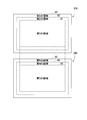
- FIG. 2 is a plan view of the first substrate 100 and the second substrate 200.
- FIG. 2 shows the positions of the first region A1 and the second region A2 on the surface 120a and the positions of the third region A3 and the fourth region A4 on the surface 220a.
- the first area A1 is an area including the center of the surface 120a.
- the second region A2 surrounds the first region A1. That is, the second area A2 is a peripheral area of the first area A1.
- the area of the second region A2 is smaller than the area of the first region A1.
- the third region A3 is a region including the center of the surface 220a.
- the fourth region A4 surrounds the third region A3. That is, the fourth area A4 is a peripheral area of the third area A3.
- the area of the fourth region A4 is smaller than the area of the third region A3.
- a plurality of first connection portions 300 are arranged in the first region A1 and the third region A3.
- the third area A3 is opposed to the first area A1.
- a plurality of second connection portions 400 are arranged in the second region A2 and the fourth region A4.
- the fourth area A4 is opposed to the second area A2.
- FIG. 3 is a plan view of the first substrate 100 and a cross-sectional view of the connection portion.
- the first bump 301, the first base electrode 302a, the second bump 401, and the second base electrode 402a before the first substrate 100 and the second substrate 200 are bonded to each other. And a cross section is shown.
- FIG. 3 schematically shows the first substrate 100 and the connection portion.
- the ratio between the width of the first substrate 100 and the height of the connection portion is different from that in the actual semiconductor device 10.
- a large number of connection portions are arranged on the surface of the first substrate 100 with high density.
- the connection portion is depicted as an aggregate of a plurality of connection portions.
- the height H22 of the second bump 401 is smaller than the height H12 of the first bump 301 on average.
- the height H22 of the second bump 401 decreases from the center of the first substrate 100 toward the outside.
- the height H21 of the second base electrode 402a is greater than the height H11 of the first base electrode 302a. Therefore, the sum of the height H21 of the second base electrode 402a and the height H22 of the second bump 401 is the sum of the height H11 of the first base electrode 302a and the height H12 of the first bump 301. Average larger than total.
- the sum of the height H21 of the second base electrode 402a and the height H22 of the second bump 401 in the outermost portion of the second region A2 is the height H11 of the first base electrode 302a and the first bump.
- the height H21 of the second base electrode 402a is set to be equal to or greater than the sum of the height H12 of 301.
- the height H22 of the second bump 401 is the height H12 of the first bump 301 in the outermost part of the second region A2. Smaller than 0.2 ⁇ m.
- the height H21 of the second base electrode 402a is 0.2 ⁇ m or more larger than the height H11 of the first base electrode 302a.
- FIG. 4 shows a state of the semiconductor device 10 before the first substrate 100 and the second substrate 200 are bonded.
- FIG. 4 shows a cross section of the semiconductor device 10.
- the sum of the height H21 of the second base electrode 402a and the height H22 of the second bump 401 is the height H11 of the first base electrode 302a and the height H12 of the first bump 301. Is greater than the sum of The height H13 of the first base electrode 302b and the height H23 of the second base electrode 402b are substantially the same. For this reason, the height of the second connection portion 400 in the thickness direction D1 of the first substrate 100 is larger than the height of the first connection portion 300 in the thickness direction.
- the second bump 401 comes into contact with the second base electrode 402b before the first bump 301 comes into contact with the first base electrode 302b. .
- the upper portion of the second bump 401 is crushed by the load. For this reason, the height H22 of the second bump 401 is reduced.
- the first bump 301 comes into contact with the first base electrode 302b.
- the first substrate 100 and the second substrate 200 are electrically connected by the first connection portion 300 and the second connection portion 400. Therefore, it is possible to reduce connection failure in the connection portion.
- the difference between the height H21 of the second base electrode 402a and the height H11 of the first base electrode 302a may be small. If the height H21 of the second base electrode 402a is higher than the height H11 of the first base electrode 302a, the difference in height between the first bump 301 and the second bump 401 becomes small. Accordingly, the first bump 301 is likely to be in contact with the first base electrode 302b, and the second bump 401 is likely to be in contact with the second base electrode 402b.
- the area of the second region A2 is smaller than the area of the first region A1, and the area of the fourth region A4 is smaller than the area of the third region A3.
- the number of the plurality of second connection portions 400 is smaller than the number of the plurality of first connection portions 300. Therefore, the load necessary for the second bump 401 to be crushed is smaller than the load necessary for the first bump 301 to be crushed. Furthermore, since the diameter L2 of the second bump 401 is smaller than the diameter L1 of the first bump 301, a load necessary for the second bump 401 to be crushed is reduced.
- FIG. 5 shows a configuration of a semiconductor device 11 according to a modification of the first embodiment.
- FIG. 5 shows a cross section of the semiconductor device 11.
- the diameter L1 of the first bump 301 and the diameter L2 of the second bump 401 are substantially the same.
- the diameter L1 of the first bump 301 and the diameter L2 of the second bump 401 are different depending on the position in the thickness direction D1 of the first substrate 100, the same in the thickness direction D1 of the first substrate 100.
- the diameter L1 of the first bump 301 and the diameter L2 of the second bump 401 are substantially the same.
- the configuration shown in FIG. 5 is the same as the configuration shown in FIG.
- the semiconductor devices 10 and 11 include the plurality of first connection portions 300, the plurality of second connection portions 400, the first substrate 100, and the second substrate 200. And have.
- Each of the plurality of first connection portions 300 includes a first bump 301 and a first base electrode 302a.
- Each of the plurality of second connection portions 400 includes a second bump 401 and a second base electrode 402a.
- the semiconductor device includes a first semiconductor layer 110, a first via 122, a first interlayer insulating film 123, a second semiconductor layer 210, a second via 222, The structure corresponding to at least one of the second interlayer insulating film 223, the first base electrode 302b, and the second base electrode 402b may not be provided.
- the semiconductor device according to each aspect of the present invention may include three or more substrates. In the case where the semiconductor device has three or more substrates, the two adjacent substrates correspond to the first substrate 100 and the second substrate 200.
- the height H21 of the second base electrode 402a in the thickness direction D1 of the first substrate 100 is larger than the height H11 of the first base electrode 302a in the thickness direction D1. For this reason, the connection failure of a connection part can be reduced.
- the diameter L2 of the second bump 401 may be smaller than the diameter L1 of the first bump 301. Thereby, a load required when the first substrate 100 and the second substrate 200 are bonded is reduced.
- FIG. 6 shows the configuration of the semiconductor device 12 according to the second embodiment of the present invention.
- FIG. 6 shows a cross section of the semiconductor device 12.
- the semiconductor device 12 includes a first substrate 100, a second substrate 200, a first connection unit 300, a second connection unit 400, and a third connection unit 500.
- the first substrate 100 and the second substrate 200 are connected via the first connection unit 300, the second connection unit 400, and the third connection unit 500.
- the first substrate 100 and the second substrate 200 are stacked in the thickness direction D1 of the first substrate 100.
- the semiconductor device 12 has a plurality of third connection portions 500.
- one third connection portion 500 is shown as a representative.
- the surface 120a includes a fifth region A5 in which a plurality of third connection portions 500 are arranged.
- the surface 220a includes a sixth region A6 in which the plurality of third connection portions 500 are disposed.
- the third connection unit 500 is disposed between the first substrate 100 and the second substrate 200.
- the third connection portion 500 is disposed in the fifth region A5 on the surface 120a, and is disposed in the sixth region A6 on the surface 220a.
- the third connection unit 500 electrically connects the first wiring 121 and the second wiring 221.
- the third connection unit 500 includes a third bump 501, a third base electrode 502a, and a third base electrode 502b.
- the third bump 501, the third base electrode 502 a, and the third base electrode 502 b are made of a fourth conductive material.
- the fourth conductive material is a metal such as gold (Au), aluminum (Al), and copper (Cu).
- the third bump 501 is disposed between the third base electrode 502a and the third base electrode 502b.
- the third bump 501 is in contact with the third base electrode 502a and the third base electrode 502b.
- the third base electrode 502a and the third base electrode 502b are disposed between any one of the fifth region A5 and the sixth region A6 and the third bump 501.
- the third base electrode 502a is disposed between the fifth region A5 and the third bump 501.
- the third base electrode 502a is in contact with the fifth region A5.
- the third base electrode 502a is in contact with the first via 122 in the fifth region A5.
- the third base electrode 502 b is disposed between the sixth region A ⁇ b> 6 and the third bump 501.
- the third base electrode 502b is in contact with the sixth region A6.
- the third base electrode 502b is in contact with the second via 222 in the sixth region A6.
- the height H31 of the third base electrode 502a in the thickness D1 direction of the first substrate 100 is larger than the height H21 of the second base electrode 402a in the thickness direction D1.
- the second base electrode 402a and the third base electrode 502a have a first layer formed at the same time.
- the second base electrode 402a and the third base electrode 502a further include a second layer that is formed simultaneously with the first layer.
- the third base electrode 502a further includes a third layer formed as the second layer.
- the height H32 of the third bump 501 in the thickness D1 direction of the first substrate 100 is smaller than the height H22 of the second bump 401 in the thickness direction D1.
- the sum of the height H21 of the second base electrode 402a and the height H22 of the second bump 401 and the sum of the height H31 of the third base electrode 502a and the height H32 of the third bump 501 are: Are almost identical.
- the height H23 of the second base electrode 402b in the thickness D1 direction of the first substrate 100 and the height H33 of the third base electrode 502b in the thickness direction D1 are substantially the same.
- the height of the second connection portion 400 in the thickness D1 direction of the first substrate 100 and the height of the third connection portion 500 in the thickness direction D1 are substantially the same.
- the height of the second connection portion 400 is the sum of the height H21 of the second base electrode 402a, the height H22 of the second bump 401, and the height H23 of the second base electrode 402b.
- the height of the third connection portion 500 is the sum of the height H31 of the third base electrode 502a, the height H32 of the third bump 501 and the height H33 of the third base electrode 502b.
- the diameter L3 of the third bump 501, the diameter L2 of the second bump 401, and the diameter L1 of the first bump 301 are substantially the same.
- the diameter L2 of the second bump 401 may be smaller than the diameter L1 of the first bump 301.
- the diameter L3 of the third bump 501 may be smaller than the diameter L2 of the second bump 401.
- the third base electrode 502b may not be arranged. That is, the third bump 501 may contact the surface 220a.
- the first base electrode 302a may be disposed in the third region A3, and the first base electrode 302b may be disposed in the first region A1.
- the second base electrode 402a may be disposed in the fourth region A4, and the second base electrode 402b may be disposed in the second region A2.
- the third base electrode 502a may be disposed in the sixth region A6, and the third base electrode 502b may be disposed in the fifth region A5.
- FIG. 7 is a plan view of the first substrate 100 and the second substrate 200.
- the first area A1 is an area including the center of the surface 120a.
- the second region A2 surrounds the first region A1. That is, the second area A2 is a peripheral area of the first area A1.
- the fifth region A5 surrounds the first region A1 and the second region A2. That is, the fifth area A5 is a peripheral area of the second area A2.
- the area of the second region A2 and the area of the fifth region A5 are smaller than the area of the first region A1.
- the third region A3 is a region including the center of the surface 220a.
- the fourth region A4 surrounds the third region A3. That is, the fourth area A4 is a peripheral area of the third area A3.
- the sixth region A6 surrounds the third region A3 and the fourth region A4. That is, the sixth area A6 is a peripheral area of the fifth area A5.
- the area of the fourth region A4 and the area of the sixth region A6 are smaller than the area of the third region A3.
- a plurality of first connection portions 300 are arranged in the first region A1 and the third region A3.
- the third area A3 is opposed to the first area A1.
- a plurality of second connection portions 400 are arranged in the second region A2 and the fourth region A4.
- the fourth area A4 is opposed to the second area A2.
- a plurality of third connection portions 500 are arranged in the fifth region A5 and the sixth region A6.
- the sixth area A6 faces the fifth area A5.
- the height H31 of the third base electrode 502a in the thickness direction D1 of the first substrate 100 is larger than the height H21 of the second base electrode 402a in the thickness direction D1.
- the height of two types of connection portions can be set, and in the second embodiment, the height of three types of connection portions can be set. For this reason, in 2nd Embodiment, the height of a connection part can be set more finely. As a result, it is possible to further reduce the connection failure of the connection portion.
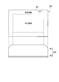
- FIG. 8 shows the configuration of the solid-state imaging device 13 according to the third embodiment of the present invention.
- the solid-state imaging device 13 is an example of a semiconductor device.
- FIG. 8 shows a cross section of the solid-state imaging device 13.
- the solid-state imaging device 13 includes a first substrate 100, a second substrate 200, a first connection unit 300, a second connection unit 400, a microlens ML, and a color filter. CF.
- the first substrate 100 and the second substrate 200 are connected via the first connection unit 300 and the second connection unit 400.
- the first substrate 100 and the second substrate 200 are stacked in the thickness direction D1 of the first substrate 100.
- the second semiconductor layer 210 includes a photoelectric conversion unit 211. Although there are a plurality of photoelectric conversion units 211 in FIG. 8, a symbol of one photoelectric conversion unit 211 is shown as a representative.
- the photoelectric conversion unit 211 is made of a second semiconductor material having an impurity concentration different from that of the second semiconductor material constituting the second semiconductor layer 210.
- the color filter CF is disposed on the surface 210b, and the microlens ML is disposed on the color filter CF.
- the microlens ML is disposed on the color filter CF.
- FIG. 8 there are a plurality of microlenses ML, but a symbol of one microlens ML is shown as a representative. Further, in FIG. 8, there are a plurality of color filters CF, but a reference numeral of one color filter CF is shown as a representative.
- the light from the subject that has passed through the imaging lens disposed optically in front of the solid-state imaging device 13 enters the microlens ML.
- the micro lens ML forms an image of light that has passed through the imaging lens.
- the color filter CF transmits light having a wavelength corresponding to a predetermined color.
- the light transmitted through the microlens ML and the color filter CF is incident on the second semiconductor layer 210.
- the light incident on the second semiconductor layer 210 travels through the second semiconductor layer 210 and enters the photoelectric conversion unit 211.
- the photoelectric conversion unit 211 converts incident light into a signal.
- the solid-state imaging device 13 may include a third connection unit 500 illustrated in FIG.
- the height H21 of the second base electrode 402a in the thickness direction D1 of the first substrate 100 is larger than the height H11 of the first base electrode 302a in the thickness direction D1. For this reason, the connection failure of a connection part can be reduced.
- Solid-state imaging device 100 1st board
Landscapes
- Solid State Image Pick-Up Elements (AREA)
- Internal Circuitry In Semiconductor Integrated Circuit Devices (AREA)
- Wire Bonding (AREA)
- Engineering & Computer Science (AREA)
- Manufacturing & Machinery (AREA)
Abstract
半導体装置は、複数の第1の接続部と、複数の第2の接続部と、第1の基板と、第2の基板とを有する。前記複数の第1の接続部のそれぞれは、第1のバンプと第1の下地電極とを有する。前記複数の第2の接続部のそれぞれは、第2のバンプと第2の下地電極とを有する。前記第1の基板の第1の面は、前記複数の第1の接続部が配置される第1の領域と、前記複数の第2の接続部が配置される第2の領域とを含む。前記第2の基板の第2の面は、前記複数の第1の接続部が配置される第3の領域と、前記複数の第2の接続部が配置される第4の領域とを含む。前記第1の面において、前記第2の領域は前記第1の領域を囲む。前記第2の面において、前記第4の領域は前記第3の領域を囲む。前記第1の基板の厚さ方向における前記第2の下地電極の高さは、前記厚さ方向における前記第1の下地電極の高さよりも大きい。
Description
本発明は、半導体装置に関する。
積層型の固体撮像装置は2枚の基板(画素ウエハおよび読み出しウエハ)を有する。画素ウエハは、複数の画素を有する。読み出しウエハは、複数の画素からの信号を読み出す回路を有する。2枚のウエハの接続方法が検討されている。例えば、微細なバンプ電極により画素毎に2枚のウエハを接続する第1の方法がある。あるいは、ライン毎に画素周辺で2枚のウエハを接続する第2の方法がある。第1の方法では、より微細なバンプ電極が必要である。バンプ電極として、半田バンプ電極、銅(Cu)バンプ電極、および金(Au)バンプ電極などが検討されている。特に、積層型の固体撮像装置の電極として、微細な金(Au)バンプ電極を用いた電極構造が検討されている。
金(Au)バンプ電極の形成方法として、電解メッキと無電解メッキとがある。電解メッキでは、シード層に電流が流れることにより電界が発生し、かつ、メッキ浴に曝露されているシード層面のみに金属の構造物が形成される。無電解メッキでは、メッキ浴に曝露されている金属面のみに金属の構造物が形成される。メッキが行われる前にシード層をパターニングできる無電解メッキにより形成されたバンプ電極のウエハ面内における高さのばらつきは、電解メッキに比べると小さい。
電解メッキのレートは速いが、ウエハ面内のレートが電界分布に依存する。電解メッキ後のシード層の除去工程があるため、電解メッキは微細構造の形成に適していない。一方、無電解メッキのレートは遅いが、ウエハ面内のバンプ電極の高さのばらつきが小さい。また、無電解メッキは、メッキ前にシード層をパターニングできるため、微細構造の形成に適している。
しかしながら、無電解メッキにより形成されたバンプ電極を介して2枚の基板が積層された固体撮像装置において、バンプ電極の接続不良が発生する。以下では、バンプ電極の接続不良について説明する。
図9は、基板800の平面図と接続部900の断面図とである。基板800は、固体撮像装置を構成する2枚の基板の1つである。接続部900は、基板800と他の基板とを電気的に接続する。接続部900は、バンプ901と下地電極902とを有する。バンプ901は、下地電極902の表面に配置されている。下地電極902は、基板800の表面に配置されている。
図9では、基板800と接続部900とは、模式的に示されている。例えば、基板800の幅と接続部900の高さとの比は、実際の固体撮像装置におけるその比と異なる。多数の接続部900が基板800の表面に高密度に配置される。図9では、接続部900は複数の接続部の集合体として描かれている。
無電解メッキ後のバンプ901には高さのばらつきがある。基板800の中心領域A11におけるバンプ901の高さのばらつきは小さい。しかし、中心領域A11を囲む周辺領域A12におけるバンプ901の高さのばらつきは大きい。周辺領域A12におけるバンプ901の高さは、中心領域A11におけるバンプ901の高さよりも平均的に小さい。周辺領域A12におけるバンプ901の高さは、基板800の中心から外側に向かって小さくなる傾向がある。中心領域A11におけるバンプ901の高さと、周辺領域A12の最も外側の部分におけるバンプ901の高さとの差は、約数百nmである。この差は、中心領域A11におけるバンプ901の高さに対して約5%である。
基板800と他の基板とは、接続部900を介して接続される。周辺領域A12におけるバンプ901の高さのばらつきにより、周辺領域A12に配置されたバンプ901が他の基板と接続されない場合がある。つまり、周辺領域A12におけるバンプ901の接続不良が発生する。固体撮像装置において、中心領域A11と周辺領域A12とは、画素が配置される画素領域である。このため、周辺領域A12において接続不良による欠陥画素が発生する。
無電解メッキ後の画素領域におけるバンプ電極の高さのばらつきを小さくする幾つかの方法が検討されている。1つの方法は、化学的機械的研磨法(CMP:Chemical Mechanical Polishing)である。この方法では、研磨パッドによる機械的な研磨と同時に、スラリーと呼ばれる化学薬品によりバンプ電極がエッチングされる。これによって、バンプ電極上部の表面が平坦化される。他の1つの方法は、バイト切削装置を用いる方法である(特許文献1参照)。この方法では、バンプ電極上部をバイトで切削することにより、バンプ電極上部の表面が平坦化される。
しかしながら、バンプ電極上部の表面を平坦にする上記の方法には以下の不具合がある。化学的機械的研磨法(CMP)では、バンプ電極の頭頂部が研磨パッドにより直接研磨される。バンプ電極と下地電極との境界部分に回転方向の力が加わるため、バンプ電極が下地電極から剥がれることがある。バンプ電極がより小さくなるほど境界部分の面積は小さくなる。このため、バンプ電極が微細である場合、バンプ電極が下地電極から剥がれやすい。さらに、バンプ電極が金(Au)などの柔らかい材料で構成される場合、研磨後のバンプ電極の頭頂部にバリが発生する。化学的機械的研磨法(CMP)は、研磨により表面を平坦化する方法である。このため、化学的機械的研磨法(CMP)は、高さが異なるバンプ電極の高さを揃える方法としてあまり適していない。
バイト切削装置を用いる方法では、化学的機械的研磨法(CMP)と同様にバンプ電極が下地電極から剥がれることがある。さらに、化学的機械的研磨法(CMP)と同様に、バンプ電極の頭頂部にバリが発生する。加えて、バイトによる切削痕が固体撮像装置の電気特性に影響する。バンプ電極が微細である場合、固体撮像装置の電気特性への影響が顕著に現れる。切削毎の小さな高さばらつきが原因である。切削痕を解消するために切削回数を増やすことはできる。しかし、切削回数が増えると、バンプ電極の頭頂部に回転方向のバリが発生しやすい。
本発明は、接続部の接続不良を低減することができる半導体装置を提供することを目的とする。
本発明の第1の態様によれば、半導体装置は、複数の第1の接続部と、複数の第2の接続部と、第1の基板と、第2の基板とを有する。前記複数の第1の接続部は、第1の配線と第2の配線とを電気的に接続する。前記複数の第2の接続部は、前記第1の配線と前記第2の配線とを電気的に接続する。前記第1の基板は、第1の面と前記第1の配線とを有し、かつ、第1の半導体材料を含む。前記第1の面は、前記複数の第1の接続部が配置される第1の領域と、前記複数の第2の接続部が配置される第2の領域とを含む。前記第2の基板は、第2の面と前記第2の配線とを有し、かつ、第2の半導体材料を含む。前記第2の面は前記第1の面と対向する。前記第2の面は、前記複数の第1の接続部が配置される第3の領域と、前記複数の第2の接続部が配置される第4の領域とを含む。前記複数の第1の接続部のそれぞれは、第1のバンプと第1の下地電極とを有する。前記第1の下地電極は、前記第1の領域と前記第3の領域とのいずれか1つと前記第1のバンプとの間に配置される。前記複数の第2の接続部のそれぞれは、第2のバンプと第2の下地電極とを有する。前記第2の下地電極は、前記第2の領域と前記第4の領域とのいずれか1つと前記第2のバンプとの間に配置される。前記第1の面において、前記第2の領域は前記第1の領域を囲む。前記第2の面において、前記第4の領域は前記第3の領域を囲む。前記第1の基板の厚さ方向における前記第2の下地電極の高さは、前記厚さ方向における前記第1の下地電極の高さよりも大きい。
本発明の第2の態様によれば、第1の態様において、前記第2のバンプの径は、前記第1のバンプの径よりも小さくてもよい。
本発明の第3の態様によれば、第1の態様において、前記半導体装置は、前記第1の配線と前記第2の配線とを電気的に接続する複数の第3の接続部をさらに有してもよい。前記第1の面は、前記複数の第3の接続部が配置される第5の領域をさらに含んでもよい。前記第2の面は、前記複数の第3の接続部が配置される第6の領域をさらに含んでもよい。前記複数の第3の接続部のそれぞれは、第3のバンプと第3の下地電極とを有する。前記第3の下地電極は、前記第5の領域と前記第6の領域とのいずれか1つと前記第3のバンプとの間に配置される。前記第1の面において、前記第5の領域は前記第1の領域と前記第2の領域とを囲む。前記第2の面において、前記第6の領域は前記第3の領域と前記第4の領域とを囲む。前記厚さ方向における前記第3の下地電極の高さは、前記厚さ方向における前記第2の下地電極の高さよりも大きくてもよい。
本発明の第4の態様によれば、第1の態様において、前記厚さ方向における前記第2の接続部の高さは、前記厚さ方向における前記第1の接続部の高さよりも大きくてもよい。
上記の各態様によれば、第1の基板の厚さ方向における第2の下地電極の高さは、その厚さ方向における第1の下地電極の高さよりも大きい。このため、接続部の接続不良を低減することができる。
図面を参照し、本発明の実施形態を説明する。
(第1の実施形態)
図1は、本発明の第1の実施形態の半導体装置10の構成を示している。図1では半導体装置10の断面が示されている。図1に示すように、半導体装置10は、第1の基板100と、第2の基板200と、第1の接続部300と、第2の接続部400とを有する。第1の基板100と第2の基板200とは、第1の接続部300と第2の接続部400とを介して接続されている。第1の基板100と第2の基板200とは、第1の基板100の厚さ方向D1に積層されている。
図1は、本発明の第1の実施形態の半導体装置10の構成を示している。図1では半導体装置10の断面が示されている。図1に示すように、半導体装置10は、第1の基板100と、第2の基板200と、第1の接続部300と、第2の接続部400とを有する。第1の基板100と第2の基板200とは、第1の接続部300と第2の接続部400とを介して接続されている。第1の基板100と第2の基板200とは、第1の基板100の厚さ方向D1に積層されている。
半導体装置10は、複数の第1の接続部300を有する。図1では、代表として1つの第1の接続部300が示されている。半導体装置10は、複数の第2の接続部400を有する。図1では、代表として1つの第2の接続部400が示されている。
半導体装置10を構成する部分の寸法は、図1に示される寸法に従うわけではない。半導体装置10を構成する部分の寸法は任意であってよい。図1では、半導体装置10を構成する部分の高さは、第1の基板100の厚さ方向D1の長さとして示される。
第1の基板100は、第1の半導体層110と、第1の配線層120とを有する。第1の半導体層110と第1の配線層120とは、第1の基板100の厚さ方向D1に重なっている。また、第1の半導体層110と第1の配線層120とは互いに接触している。
第1の半導体層110は、第1の半導体材料で構成されている。つまり、第1の基板100は、第1の半導体材料を含む。例えば、第1の半導体材料は、シリコン(Si)である。第1の半導体層110は、面110aと面110bとを有する。面110aと面110bとは、反対方向を向いている。面110aは、第1の配線層120と接触している。面110bは、第1の基板100の主面の1つを構成する。主面は、基板の表面を構成する複数の面のうち最も広い面である。
第1の配線層120は、第1の配線121と、第1のビア122と、第1の層間絶縁膜123とを有する。図1では複数の第1の配線121が存在するが、代表として1つの第1の配線121の符号が示されている。図1では複数の第1のビア122が存在するが、代表として1つの第1のビア122の符号が示されている。
第1の配線層120は、面120a(第1の面)と面120bとを有する。面120aは第2の基板200と対向する。面120aは、第1の接続部300および第2の接続部400と接触している。面120bは第1の半導体層110と接触している。面120aは第1の基板100の主面の1つを構成する。
第1の配線121と第1のビア122とは、第1の導電材料で構成されている。例えば、第1の導電材料は、アルミニウム(Al)および銅(Cu)等の金属である。第1の配線121は、配線パターンが形成された薄膜である。第1の配線121は、信号を伝送する。1層のみの第1の配線121が形成されていてもよいし、複数層の第1の配線121が形成されていてもよい。図1に示す例では、2層の第1の配線121が形成されている。
第1のビア122は、異なる層の第1の配線121を接続する。第1の配線層120において、第1の配線121および第1のビア122以外の部分は、第1の層間絶縁膜123で構成されている。第1の層間絶縁膜123は、第1の絶縁材料で構成されている。例えば、第1の絶縁材料は、二酸化珪素(SiO2)である。
第1の半導体層110と第1の配線層120との少なくとも一方は、トランジスタ等の回路要素を有してもよい。
第1の基板100は、面120a(第1の面)と第1の配線121とを有し、かつ、第1の半導体材料を含む。面120aは、複数の第1の接続部300が配置される第1の領域A1と、複数の第2の接続部400が配置される第2の領域A2とを含む。
第2の基板200は、第2の半導体層210と、第2の配線層220とを有する。第2の半導体層210と第2の配線層220とは、第1の基板100の厚さ方向D1に重なっている。また、第2の半導体層210と第2の配線層220とは互いに接触している。
第2の半導体層210は、第2の半導体材料で構成されている。つまり、第2の基板200は、第2の半導体材料を含む。例えば、第2の半導体材料は、シリコン(Si)である。第2の半導体層210は、面210aと面210bとを有する。面210aと面210bとは、反対方向を向いている。面210aは、第2の配線層220と接触している。面210bは、第2の基板200の主面の1つを構成する。
第2の配線層220は、第2の配線221と、第2のビア222と、第2の層間絶縁膜223とを有する。図1では複数の第2の配線221が存在するが、代表として1つの第2の配線221の符号が示されている。図1では複数の第2のビア222が存在するが、代表として1つの第2のビア222の符号が示されている。
第2の配線層220は、面220a(第2の面)と面220bとを有する。面220aは第1の基板100と対向する。面220aは、第1の接続部300および第2の接続部400と接触している。面220bは第2の半導体層210と接触している。面220aは第2の基板200の主面の1つを構成する。
第2の配線221と第2のビア222とは、第2の導電材料で構成されている。例えば、第2の導電材料は、アルミニウム(Al)および銅(Cu)等の金属である。第2の配線221は、配線パターンが形成された薄膜である。第2の配線221は、信号を伝送する。1層のみの第2の配線221が形成されていてもよいし、複数層の第2の配線221が形成されていてもよい。図1に示す例では、2層の第2の配線221が形成されている。
第2のビア222は、異なる層の第2の配線221を接続する。第2の配線層220において、第2の配線221および第2のビア222以外の部分は、第2の層間絶縁膜223で構成されている。第2の層間絶縁膜223は、第2の絶縁材料で構成されている。例えば、第2の絶縁材料は、二酸化珪素(SiO2)である。
第2の半導体層210と第2の配線層220との少なくとも一方は、トランジスタ等の回路要素を有してもよい。
第2の基板200は、面220a(第2の面)と第2の配線221とを有し、かつ、第2の半導体材料を含む。面220aは面120aと対向する。面220aは、複数の第1の接続部300が配置される第3の領域A3と、複数の第2の接続部400が配置される第4の領域A4とを含む。
第1の接続部300と第2の接続部400とは、第1の基板100と第2の基板200との間に配置されている。第1の接続部300は、面120aにおいて第1の領域A1に配置され、かつ、面220aにおいて第3の領域A3に配置されている。第2の接続部400は、面120aにおいて第2の領域A2に配置され、かつ、面220aにおいて第4の領域A4に配置されている。第1の接続部300と第2の接続部400とは、第1の配線121と第2の配線221とを電気的に接続する。
第1の接続部300は、第1のバンプ301と、第1の下地電極302aと、第1の下地電極302bとを有する。第1のバンプ301と、第1の下地電極302aと、第1の下地電極302bとは、第3の導電材料で構成されている。例えば、第3の導電材料は、金(Au)、アルミニウム(Al)、および銅(Cu)等の金属である。
第1のバンプ301は、第1の下地電極302aと第1の下地電極302bとの間に配置されている。第1のバンプ301は、第1の下地電極302aおよび第1の下地電極302bと接触している。第1の下地電極302aと第1の下地電極302bとは、第1の領域A1と第3の領域A3とのいずれか1つと第1のバンプ301との間に配置されている。図1では、第1の下地電極302aは、第1の領域A1と第1のバンプ301との間に配置されている。第1の下地電極302aは、第1の領域A1と接触している。第1の下地電極302aは、第1の領域A1において、第1のビア122と接触している。図1では、第1の下地電極302bは、第3の領域A3と第1のバンプ301との間に配置されている。第1の下地電極302bは、第3の領域A3と接触している。第1の下地電極302bは、第3の領域A3において、第2のビア222と接触している。
第2の接続部400は、第2のバンプ401と、第2の下地電極402aと、第2の下地電極402bとを有する。第2のバンプ401と、第2の下地電極402aと、第2の下地電極402bとは、第4の導電材料で構成されている。例えば、第4の導電材料は、金(Au)、アルミニウム(Al)、および銅(Cu)等の金属である。
第2のバンプ401は、第2の下地電極402aと第2の下地電極402bとの間に配置されている。第2のバンプ401は、第2の下地電極402aおよび第2の下地電極402bと接触している。第2の下地電極402aと第2の下地電極402bとは、第2の領域A2と第4の領域A4とのいずれか1つと第2のバンプ401との間に配置されている。図1では、第2の下地電極402aは、第2の領域A2と第2のバンプ401との間に配置されている。第2の下地電極402aは、第2の領域A2と接触している。第2の下地電極402aは、第2の領域A2において、第1のビア122と接触している。図1では、第2の下地電極402bは、第4の領域A4と第2のバンプ401との間に配置されている。第2の下地電極402bは、第4の領域A4と接触している。第2の下地電極402bは、第4の領域A4において、第2のビア222と接触している。
第1の基板100の厚さD1方向における第2の下地電極402aの高さH21は、その厚さ方向D1における第1の下地電極302aの高さH11よりも大きい。例えば、第1の下地電極302aと第2の下地電極402aとは、同時に形成される第1の層を有する。第2の下地電極402aは、第1の層に形成された第2の層をさらに有する。
第1の基板100の厚さD1方向における第2のバンプ401の高さH22は、その厚さ方向D1における第1のバンプ301の高さH12よりも小さい。第1の下地電極302aの高さH11と第1のバンプ301の高さH12との合計と、第2の下地電極402aの高さH21と第2のバンプ401の高さH22との合計とは、ほぼ同一である。
第1の基板100の厚さD1方向における第1の下地電極302bの高さH13と、その厚さ方向D1における第2の下地電極402bの高さH23とは、ほぼ同一である。このため、第1の基板100の厚さD1方向における第1の接続部300の高さと、その厚さ方向D1における第2の接続部400の高さとは、ほぼ同一である。第1の接続部300の高さは、第1の下地電極302aの高さH11と、第1のバンプ301の高さH12と、第1の下地電極302bの高さH13との合計である。第2の接続部400の高さは、第2の下地電極402aの高さH21と、第2のバンプ401の高さH22と、第2の下地電極402bの高さH23との合計である。
第2のバンプ401の径L2は、第1のバンプ301の径L1よりも小さい。第1のバンプ301の径L1と第2のバンプ401の径L2とは、面120aに平行な断面における径である。第1のバンプ301の径L1と第2のバンプ401の径L2とが、第1の基板100の厚さ方向D1の位置に応じて異なる場合、第1の基板100の厚さ方向D1の同一位置において、第2のバンプ401の径L2は、第1のバンプ301の径L1よりも小さい。第2のバンプ401の最大径は第1のバンプ301の最小径よりも小さい。
第1の下地電極302bと第2の下地電極402bとが配置されなくてもよい。つまり、第1のバンプ301と第2のバンプ401とが面220aに接触してもよい。第1の下地電極302aが第3の領域A3に配置され、かつ、第1の下地電極302bが第1の領域A1に配置されてもよい。第2の下地電極402aが第4の領域A4に配置され、かつ、第2の下地電極402bが第2の領域A2に配置されてもよい。
図2は、第1の基板100と第2の基板200との平面図である。図2では、面120aにおける第1の領域A1と第2の領域A2との位置と、面220aにおける第3の領域A3と第4の領域A4との位置とが示されている。
第1の領域A1は、面120aの中心を含む領域である。面120aにおいて、第2の領域A2は第1の領域A1を囲む。つまり、第2の領域A2は、第1の領域A1の周辺領域である。第2の領域A2の面積は、第1の領域A1の面積よりも小さい。第3の領域A3は、面220aの中心を含む領域である。面220aにおいて、第4の領域A4は第3の領域A3を囲む。つまり、第4の領域A4は、第3の領域A3の周辺領域である。第4の領域A4の面積は、第3の領域A3の面積よりも小さい。
第1の領域A1と第3の領域A3とに複数の第1の接続部300が配置される。第3の領域A3は、第1の領域A1と対向する。第2の領域A2と第4の領域A4とに複数の第2の接続部400が配置される。第4の領域A4は、第2の領域A2と対向する。
図3は、第1の基板100の平面図と接続部の断面図とである。図3では、第1の基板100と第2の基板200とが接合される前の第1のバンプ301と、第1の下地電極302aと、第2のバンプ401と、第2の下地電極402aとの断面が示されている。
図3では、第1の基板100と接続部とは、模式的に示されている。例えば、第1の基板100の幅と接続部の高さとの比は、実際の半導体装置10におけるその比と異なる。多数の接続部が第1の基板100の表面に高密度に配置される。図3では、接続部は、複数の接続部の集合体として描かれている。
第1の基板100と第2の基板200とが接合される前、第2のバンプ401の高さH22は、第1のバンプ301の高さH12よりも平均的に小さい。第2のバンプ401の高さH22は、第1の基板100の中心から外側に向かって小さくなる。第1の実施形態では、第2の下地電極402aの高さH21は、第1の下地電極302aの高さH11よりも大きい。このため、第2の下地電極402aの高さH21と第2のバンプ401の高さH22との合計は、第1の下地電極302aの高さH11と第1のバンプ301の高さH12との合計よりも平均的に大きい。
第2の領域A2の最も外側の部分において第2の下地電極402aの高さH21と第2のバンプ401の高さH22との合計が第1の下地電極302aの高さH11と第1のバンプ301の高さH12との合計以上となるように第2の下地電極402aの高さH21が設定される。例えば、第1のバンプ301の高さH12が4μmである場合、第2の領域A2の最も外側の部分では第2のバンプ401の高さH22の高さは第1のバンプ301の高さH12よりも0.2μm小さい。この場合、第2の下地電極402aの高さH21は、第1の下地電極302aの高さH11よりも0.2μm以上大きい。
図4は、第1の基板100と第2の基板200とが接合される前の半導体装置10の状態を示している。図4では半導体装置10の断面が示されている。
図4では、第2の下地電極402aの高さH21と第2のバンプ401の高さH22との合計は、第1の下地電極302aの高さH11と第1のバンプ301の高さH12との合計よりも大きい。第1の下地電極302bの高さH13と第2の下地電極402bの高さH23とは、ほぼ同一である。このため、第1の基板100の厚さ方向D1における第2の接続部400の高さは、その厚さ方向における第1の接続部300の高さよりも大きい。
第1の基板100と第2の基板200とが接合されるとき、第1のバンプ301が第1の下地電極302bと接触する前に第2のバンプ401が第2の下地電極402bと接触する。荷重により、第2のバンプ401の上部が潰れる。このため、第2のバンプ401の高さH22が小さくなる。この結果、図1に示すように第1のバンプ301が第1の下地電極302bと接触する。第1の基板100と第2の基板200とが、第1の接続部300と第2の接続部400とによって電気的に接続される。したがって、接続部の接続不良を低減することができる。
第2の下地電極402aの高さH21と第1の下地電極302aの高さH11との差は、小さくてもよい。第2の下地電極402aの高さH21が第1の下地電極302aの高さH11よりも高ければ、第1のバンプ301と第2のバンプ401との高さの差が小さくなる。これによって、第1のバンプ301が第1の下地電極302bと接触しやすく、かつ、第2のバンプ401が第2の下地電極402bと接触しやすい。
第2の領域A2の面積は、第1の領域A1の面積よりも小さく、かつ、第4の領域A4の面積は、第3の領域A3の面積よりも小さい。このため、複数の第2の接続部400の数は、複数の第1の接続部300の数よりも少ない。したがって、第2のバンプ401が潰れるために必要な荷重は、第1のバンプ301が潰れるために必要な荷重よりも小さい。さらに、第2のバンプ401の径L2が第1のバンプ301の径L1よりも小さいことにより、第2のバンプ401が潰れるために必要な荷重が低減される。
図5は、第1の実施形態の変形例の半導体装置11の構成を示している。図5では半導体装置11の断面が示されている。
図5に示す構成について、図1に示す構成と異なる点を説明する。図5では、第1のバンプ301の径L1と第2のバンプ401の径L2とは、ほぼ同一である。第1のバンプ301の径L1と第2のバンプ401の径L2とが、第1の基板100の厚さ方向D1の位置に応じて異なる場合、第1の基板100の厚さ方向D1の同一位置において、第1のバンプ301の径L1と第2のバンプ401の径L2とが、ほぼ同一である。
上記の点以外の点については、図5に示す構成は、図1に示す構成と同様である。
上記のように、第1の実施形態の半導体装置10,11は、複数の第1の接続部300と、複数の第2の接続部400と、第1の基板100と、第2の基板200とを有する。複数の第1の接続部300のそれぞれは、第1のバンプ301と第1の下地電極302aとを有する。複数の第2の接続部400のそれぞれは、第2のバンプ401と第2の下地電極402aとを有する。
本発明の各態様の半導体装置は、第1の半導体層110と、第1のビア122と、第1の層間絶縁膜123と、第2の半導体層210と、第2のビア222と、第2の層間絶縁膜223と、第1の下地電極302bと、第2の下地電極402bとの少なくとも1つに対応する構成を有していなくてもよい。本発明の各態様の半導体装置は、3枚以上の基板を有してもよい。半導体装置が3枚以上の基板を有する場合、隣接する2枚の基板が第1の基板100と第2の基板200とに対応する。
第1の実施形態では、第1の基板100の厚さ方向D1における第2の下地電極402aの高さH21は、その厚さ方向D1における第1の下地電極302aの高さH11よりも大きい。このため、接続部の接続不良を低減することができる。
第2のバンプ401の径L2は、第1のバンプ301の径L1よりも小さくてもよい。これによって、第1の基板100と第2の基板200とが接合されるときに必要な荷重が低減される。
(第2の実施形態)
図6は、本発明の第2の実施形態の半導体装置12の構成を示している。図6では半導体装置12の断面が示されている。図6に示すように、半導体装置12は、第1の基板100と、第2の基板200と、第1の接続部300と、第2の接続部400と、第3の接続部500とを有する。第1の基板100と第2の基板200とは、第1の接続部300と、第2の接続部400と、第3の接続部500とを介して接続されている。第1の基板100と第2の基板200とは、第1の基板100の厚さ方向D1に積層されている。
図6は、本発明の第2の実施形態の半導体装置12の構成を示している。図6では半導体装置12の断面が示されている。図6に示すように、半導体装置12は、第1の基板100と、第2の基板200と、第1の接続部300と、第2の接続部400と、第3の接続部500とを有する。第1の基板100と第2の基板200とは、第1の接続部300と、第2の接続部400と、第3の接続部500とを介して接続されている。第1の基板100と第2の基板200とは、第1の基板100の厚さ方向D1に積層されている。
図6に示す構成について、図1に示す構成と異なる点を説明する。半導体装置12は、複数の第3の接続部500を有する。図6では、代表として1つの第3の接続部500が示されている。
面120aは、複数の第3の接続部500が配置される第5の領域A5を含む。面220aは、複数の第3の接続部500が配置される第6の領域A6を含む。
第3の接続部500は、第1の基板100と第2の基板200との間に配置されている。第3の接続部500は、面120aにおいて第5の領域A5に配置され、かつ、面220aにおいて第6の領域A6に配置されている。第3の接続部500は、第1の配線121と第2の配線221とを電気的に接続する。
第3の接続部500は、第3のバンプ501と、第3の下地電極502aと、第3の下地電極502bとを有する。第3のバンプ501と、第3の下地電極502aと、第3の下地電極502bとは、第4の導電材料で構成されている。例えば、第4の導電材料は、金(Au)、アルミニウム(Al)、および銅(Cu)等の金属である。
第3のバンプ501は、第3の下地電極502aと第3の下地電極502bとの間に配置されている。第3のバンプ501は、第3の下地電極502aおよび第3の下地電極502bと接触している。第3の下地電極502aと第3の下地電極502bとは、第5の領域A5と第6の領域A6とのいずれか1つと第3のバンプ501との間に配置されている。図6では、第3の下地電極502aは、第5の領域A5と第3のバンプ501との間に配置されている。第3の下地電極502aは、第5の領域A5と接触している。第3の下地電極502aは、第5の領域A5において、第1のビア122と接触している。図6では、第3の下地電極502bは、第6の領域A6と第3のバンプ501との間に配置されている。第3の下地電極502bは、第6の領域A6と接触している。第3の下地電極502bは、第6の領域A6において、第2のビア222と接触している。
第1の基板100の厚さD1方向における第3の下地電極502aの高さH31は、その厚さ方向D1における第2の下地電極402aの高さH21よりも大きい。例えば、第2の下地電極402aと第3の下地電極502aとは、同時に形成される第1の層を有する。第2の下地電極402aと第3の下地電極502aとは、第1の層に同時に形成される第2の層をさらに有する。第3の下地電極502aは、第2の層に形成された第3の層をさらに有する。
第1の基板100の厚さD1方向における第3のバンプ501の高さH32は、その厚さ方向D1における第2のバンプ401の高さH22よりも小さい。第2の下地電極402aの高さH21と第2のバンプ401の高さH22との合計と、第3の下地電極502aの高さH31と第3のバンプ501の高さH32との合計とは、ほぼ同一である。
第1の基板100の厚さD1方向における第2の下地電極402bの高さH23と、その厚さ方向D1における第3の下地電極502bの高さH33とは、ほぼ同一である。このため、第1の基板100の厚さD1方向における第2の接続部400の高さと、その厚さ方向D1における第3の接続部500の高さとは、ほぼ同一である。第2の接続部400の高さは、第2の下地電極402aの高さH21と、第2のバンプ401の高さH22と、第2の下地電極402bの高さH23との合計である。第3の接続部500の高さは、第3の下地電極502aの高さH31と、第3のバンプ501の高さH32と、第3の下地電極502bの高さH33との合計である。
第3のバンプ501の径L3と、第2のバンプ401の径L2と、第1のバンプ301の径L1とは、ほぼ同一である。第2のバンプ401の径L2は、第1のバンプ301の径L1よりも小さくてもよい。第3のバンプ501の径L3は、第2のバンプ401の径L2よりも小さくてもよい。
第3の下地電極502bが配置されなくてもよい。つまり、第3のバンプ501が面220aに接触してもよい。第1の下地電極302aが第3の領域A3に配置され、かつ、第1の下地電極302bが第1の領域A1に配置されてもよい。第2の下地電極402aが第4の領域A4に配置され、かつ、第2の下地電極402bが第2の領域A2に配置されてもよい。第3の下地電極502aが第6の領域A6に配置され、かつ、第3の下地電極502bが第5の領域A5に配置されてもよい。
上記以外の点については、図6に示す構成は図1に示す構成と同様である。
図7は、第1の基板100と第2の基板200との平面図である。図7では、面120aにおける第1の領域A1と第2の領域A2と第5の領域A5との位置と、面220aにおける第3の領域A3と第4の領域A4と第6の領域A6との位置とが示されている。
第1の領域A1は、面120aの中心を含む領域である。面120aにおいて、第2の領域A2は第1の領域A1を囲む。つまり、第2の領域A2は、第1の領域A1の周辺領域である。面120aにおいて、第5の領域A5は第1の領域A1と第2の領域A2とを囲む。つまり、第5の領域A5は、第2の領域A2の周辺領域である。第2の領域A2の面積と第5の領域A5の面積とは、第1の領域A1の面積よりも小さい。
第3の領域A3は、面220aの中心を含む領域である。面220aにおいて、第4の領域A4は第3の領域A3を囲む。つまり、第4の領域A4は、第3の領域A3の周辺領域である。面220aにおいて、第6の領域A6は第3の領域A3と第4の領域A4とを囲む。つまり、第6の領域A6は、第5の領域A5の周辺領域である。第4の領域A4の面積と第6の領域A6の面積とは、第3の領域A3の面積よりも小さい。
第1の領域A1と第3の領域A3とに複数の第1の接続部300が配置される。第3の領域A3は、第1の領域A1と対向する。第2の領域A2と第4の領域A4とに複数の第2の接続部400が配置される。第4の領域A4は、第2の領域A2と対向する。第5の領域A5と第6の領域A6とに複数の第3の接続部500が配置される。第6の領域A6は、第5の領域A5と対向する。
第2の実施形態では、第1の基板100の厚さ方向D1における第3の下地電極502aの高さH31は、その厚さ方向D1における第2の下地電極402aの高さH21よりも大きい。第1の実施形態では2種類の接続部の高さが設定でき、第2の実施形態では3種類の接続部の高さが設定できる。このため、第2の実施形態では、接続部の高さをより細かく設定することができる。この結果、接続部の接続不良をさらに低減することができる。
(第3の実施形態)
図8は、本発明の第3の実施形態の固体撮像装置13の構成を示している。固体撮像装置13は、半導体装置の1つの例である。図8では固体撮像装置13の断面が示されている。図8に示すように、固体撮像装置13は、第1の基板100と、第2の基板200と、第1の接続部300と、第2の接続部400と、マイクロレンズMLと、カラーフィルタCFとを有する。第1の基板100と第2の基板200とは、第1の接続部300と第2の接続部400とを介して接続されている。第1の基板100と第2の基板200とは、第1の基板100の厚さ方向D1に積層されている。
図8は、本発明の第3の実施形態の固体撮像装置13の構成を示している。固体撮像装置13は、半導体装置の1つの例である。図8では固体撮像装置13の断面が示されている。図8に示すように、固体撮像装置13は、第1の基板100と、第2の基板200と、第1の接続部300と、第2の接続部400と、マイクロレンズMLと、カラーフィルタCFとを有する。第1の基板100と第2の基板200とは、第1の接続部300と第2の接続部400とを介して接続されている。第1の基板100と第2の基板200とは、第1の基板100の厚さ方向D1に積層されている。
図8に示す構成について、図1に示す構成と異なる点を説明する。第2の半導体層210は、光電変換部211を有する。図8では複数の光電変換部211が存在するが、代表として1つの光電変換部211の符号が示されている。例えば、光電変換部211は、第2の半導体層210を構成する第2の半導体材料とは不純物濃度が異なる第2の半導体材料で構成されている。
面210bにカラーフィルタCFが配置され、かつ、カラーフィルタCF上にマイクロレンズMLが配置されている。図8では複数のマイクロレンズMLが存在するが、代表として1つのマイクロレンズMLの符号が示されている。また、図8では複数のカラーフィルタCFが存在するが、代表として1つのカラーフィルタCFの符号が示されている。
固体撮像装置13の光学的前方に配置された撮像レンズを通過した、被写体からの光がマイクロレンズMLに入射する。マイクロレンズMLは、撮像レンズを透過した光を結像する。カラーフィルタCFは、所定の色に対応した波長の光を透過させる。
マイクロレンズMLとカラーフィルタCFとを透過した光は、第2の半導体層210に入射する。第2の半導体層210に入射した光は、第2の半導体層210内を進んで光電変換部211に入射する。光電変換部211は、入射した光を信号に変換する。
上記以外の点については、図8に示す構成は図1に示す構成と同様である。
固体撮像装置13は、図6に示す第3の接続部500を有してもよい。
第3の実施形態では、第1の基板100の厚さ方向D1における第2の下地電極402aの高さH21は、その厚さ方向D1における第1の下地電極302aの高さH11よりも大きい。このため、接続部の接続不良を低減することができる。
以上、本発明の好ましい実施形態を説明したが、本発明はこれら実施形態およびその変形例に限定されることはない。本発明の趣旨を逸脱しない範囲で、構成の付加、省略、置換、およびその他の変更が可能である。また、本発明は前述した説明によって限定されることはなく、添付のクレームの範囲によってのみ限定される。
本発明の各実施形態によれば、接続部の接続不良を低減することができる。
10,11,12 半導体装置
13 固体撮像装置
100 第1の基板
110 第1の半導体層
120 第1の配線層
121 第1の配線
122 第1のビア
123 第1の層間絶縁膜
200 第2の基板
210 第2の半導体層
211 光電変換部
220 第2の配線層
221 第2の配線
222 第2のビア
223 第2の層間絶縁膜
300 第1の接続部
301 第1のバンプ
302a,302b 第1の下地電極
400 第2の接続部
401 第2のバンプ
402a,402b 第2の下地電極
500 第3の接続部
501 第3のバンプ
502a,502b 第3の下地電極
13 固体撮像装置
100 第1の基板
110 第1の半導体層
120 第1の配線層
121 第1の配線
122 第1のビア
123 第1の層間絶縁膜
200 第2の基板
210 第2の半導体層
211 光電変換部
220 第2の配線層
221 第2の配線
222 第2のビア
223 第2の層間絶縁膜
300 第1の接続部
301 第1のバンプ
302a,302b 第1の下地電極
400 第2の接続部
401 第2のバンプ
402a,402b 第2の下地電極
500 第3の接続部
501 第3のバンプ
502a,502b 第3の下地電極
Claims (4)
- 第1の配線と第2の配線とを電気的に接続する複数の第1の接続部と、
前記第1の配線と前記第2の配線とを電気的に接続する複数の第2の接続部と、
第1の面と前記第1の配線とを有し、かつ、第1の半導体材料を含み、前記第1の面は、前記複数の第1の接続部が配置される第1の領域と、前記複数の第2の接続部が配置される第2の領域とを含む第1の基板と、
第2の面と前記第2の配線とを有し、かつ、第2の半導体材料を含み、前記第2の面は前記第1の面に対向し、前記第2の面は、前記複数の第1の接続部が配置される第3の領域と、前記複数の第2の接続部が配置される第4の領域とを含む第2の基板と、
を有し、
前記複数の第1の接続部のそれぞれは、
第1のバンプと、
前記第1の領域と前記第3の領域とのいずれか1つと前記第1のバンプとの間に配置された第1の下地電極と、
を有し、
前記複数の第2の接続部のそれぞれは、
第2のバンプと、
前記第2の領域と前記第4の領域とのいずれか1つと前記第2のバンプとの間に配置された第2の下地電極と、
を有し、
前記第1の面において、前記第2の領域は前記第1の領域を囲み、
前記第2の面において、前記第4の領域は前記第3の領域を囲み、
前記第1の基板の厚さ方向における前記第2の下地電極の高さは、前記厚さ方向における前記第1の下地電極の高さよりも大きい
半導体装置。 - 前記第2のバンプの径は、前記第1のバンプの径よりも小さい
請求項1に記載の半導体装置。 - 前記半導体装置は、前記第1の配線と前記第2の配線とを電気的に接続する複数の第3の接続部をさらに有し、
前記第1の面は、前記複数の第3の接続部が配置される第5の領域をさらに含み、
前記第2の面は、前記複数の第3の接続部が配置される第6の領域をさらに含み、
前記複数の第3の接続部のそれぞれは、
第3のバンプと、
前記第5の領域と前記第6の領域とのいずれか1つと前記第3のバンプとの間に配置された第3の下地電極と、
を有し、
前記第1の面において、前記第5の領域は前記第1の領域と前記第2の領域とを囲み、
前記第2の面において、前記第6の領域は前記第3の領域と前記第4の領域とを囲み、
前記厚さ方向における前記第3の下地電極の高さは、前記厚さ方向における前記第2の下地電極の高さよりも大きい
請求項1に記載の半導体装置。 - 前記厚さ方向における前記第2の接続部の高さは、前記厚さ方向における前記第1の接続部の高さよりも大きい
請求項1に記載の半導体装置。
Priority Applications (3)
| Application Number | Priority Date | Filing Date | Title |
|---|---|---|---|
| JP2017515319A JP6474892B2 (ja) | 2015-04-28 | 2015-04-28 | 半導体装置 |
| PCT/JP2015/062805 WO2016174733A1 (ja) | 2015-04-28 | 2015-04-28 | 半導体装置 |
| US15/793,173 US10056344B2 (en) | 2015-04-28 | 2017-10-25 | Semiconductor device |
Applications Claiming Priority (1)
| Application Number | Priority Date | Filing Date | Title |
|---|---|---|---|
| PCT/JP2015/062805 WO2016174733A1 (ja) | 2015-04-28 | 2015-04-28 | 半導体装置 |
Related Child Applications (1)
| Application Number | Title | Priority Date | Filing Date |
|---|---|---|---|
| US15/793,173 Continuation US10056344B2 (en) | 2015-04-28 | 2017-10-25 | Semiconductor device |
Publications (1)
| Publication Number | Publication Date |
|---|---|
| WO2016174733A1 true WO2016174733A1 (ja) | 2016-11-03 |
Family
ID=57198280
Family Applications (1)
| Application Number | Title | Priority Date | Filing Date |
|---|---|---|---|
| PCT/JP2015/062805 Ceased WO2016174733A1 (ja) | 2015-04-28 | 2015-04-28 | 半導体装置 |
Country Status (3)
| Country | Link |
|---|---|
| US (1) | US10056344B2 (ja) |
| JP (1) | JP6474892B2 (ja) |
| WO (1) | WO2016174733A1 (ja) |
Families Citing this family (1)
| Publication number | Priority date | Publication date | Assignee | Title |
|---|---|---|---|---|
| JP7614897B2 (ja) * | 2021-03-19 | 2025-01-16 | キオクシア株式会社 | 半導体装置 |
Citations (5)
| Publication number | Priority date | Publication date | Assignee | Title |
|---|---|---|---|---|
| JP2005109000A (ja) * | 2003-09-29 | 2005-04-21 | Seiko Epson Corp | 配線基板、配線基板の製造方法、基板接合体、基板接合体の製造方法、電気光学装置、及び電気光学装置の製造方法 |
| JP2006041011A (ja) * | 2004-07-23 | 2006-02-09 | Optrex Corp | Icチップおよび表示装置 |
| JP2007194274A (ja) * | 2006-01-17 | 2007-08-02 | Nec Electronics Corp | 半導体装置の製造方法 |
| JP2011003586A (ja) * | 2009-06-16 | 2011-01-06 | Fujitsu Semiconductor Ltd | 半導体素子及びその製造方法 |
| JP2013089919A (ja) * | 2011-10-21 | 2013-05-13 | Hamamatsu Photonics Kk | 光検出装置 |
Family Cites Families (3)
| Publication number | Priority date | Publication date | Assignee | Title |
|---|---|---|---|---|
| WO2004061935A1 (ja) | 2002-12-27 | 2004-07-22 | Fujitsu Limited | バンプの形成方法、半導体装置及びその製造方法、並びに基板処理装置及び半導体製造装置 |
| CN103208501B (zh) * | 2012-01-17 | 2017-07-28 | 奥林巴斯株式会社 | 固体摄像装置及其制造方法、摄像装置、基板、半导体装置 |
| JP6071613B2 (ja) * | 2013-02-14 | 2017-02-01 | オリンパス株式会社 | 半導体基板、半導体装置、撮像素子、および撮像装置 |
-
2015
- 2015-04-28 WO PCT/JP2015/062805 patent/WO2016174733A1/ja not_active Ceased
- 2015-04-28 JP JP2017515319A patent/JP6474892B2/ja active Active
-
2017
- 2017-10-25 US US15/793,173 patent/US10056344B2/en active Active
Patent Citations (5)
| Publication number | Priority date | Publication date | Assignee | Title |
|---|---|---|---|---|
| JP2005109000A (ja) * | 2003-09-29 | 2005-04-21 | Seiko Epson Corp | 配線基板、配線基板の製造方法、基板接合体、基板接合体の製造方法、電気光学装置、及び電気光学装置の製造方法 |
| JP2006041011A (ja) * | 2004-07-23 | 2006-02-09 | Optrex Corp | Icチップおよび表示装置 |
| JP2007194274A (ja) * | 2006-01-17 | 2007-08-02 | Nec Electronics Corp | 半導体装置の製造方法 |
| JP2011003586A (ja) * | 2009-06-16 | 2011-01-06 | Fujitsu Semiconductor Ltd | 半導体素子及びその製造方法 |
| JP2013089919A (ja) * | 2011-10-21 | 2013-05-13 | Hamamatsu Photonics Kk | 光検出装置 |
Also Published As
| Publication number | Publication date |
|---|---|
| JPWO2016174733A1 (ja) | 2018-02-22 |
| US10056344B2 (en) | 2018-08-21 |
| JP6474892B2 (ja) | 2019-02-27 |
| US20180047694A1 (en) | 2018-02-15 |
Similar Documents
| Publication | Publication Date | Title |
|---|---|---|
| US11923279B2 (en) | Semiconductor device | |
| US10249672B2 (en) | Image pickup apparatus, semiconductor apparatus, and image pickup unit | |
| US11658143B2 (en) | Bump-on-trace design for enlarge bump-to-trace distance | |
| TWI493697B (zh) | 影像感測裝置及其製造方法 | |
| US9502455B2 (en) | Optical apparatus having resin encased stacked optical and semiconductor devices | |
| KR101700489B1 (ko) | 반도체 디바이스 및 그 제조 방법 | |
| US9123618B2 (en) | Method for producing image pickup apparatus, and method for producing semiconductor apparatus | |
| JP5970747B2 (ja) | 半導体装置 | |
| JP6100480B2 (ja) | 半導体装置およびその製造方法 | |
| KR20140029178A (ko) | 반도체 장치 및 그 제조 방법 | |
| US20150087088A1 (en) | Method for producing image pickup apparatus and method for producing semiconductor apparatus | |
| JP2011071239A (ja) | 半導体装置の製造方法 | |
| TW201703163A (zh) | 半導體裝置及其製造方法 | |
| JP6474892B2 (ja) | 半導体装置 | |
| US7112881B2 (en) | Semiconductor device | |
| US20150171137A1 (en) | Method for manufacturing semiconductor device |
Legal Events
| Date | Code | Title | Description |
|---|---|---|---|
| 121 | Ep: the epo has been informed by wipo that ep was designated in this application |
Ref document number: 15890717 Country of ref document: EP Kind code of ref document: A1 |
|
| ENP | Entry into the national phase |
Ref document number: 2017515319 Country of ref document: JP Kind code of ref document: A |
|
| NENP | Non-entry into the national phase |
Ref country code: DE |
|
| 122 | Ep: pct application non-entry in european phase |
Ref document number: 15890717 Country of ref document: EP Kind code of ref document: A1 |