WO2016171098A1 - 過電流保護付き電源装置 - Google Patents
過電流保護付き電源装置 Download PDFInfo
- Publication number
- WO2016171098A1 WO2016171098A1 PCT/JP2016/062234 JP2016062234W WO2016171098A1 WO 2016171098 A1 WO2016171098 A1 WO 2016171098A1 JP 2016062234 W JP2016062234 W JP 2016062234W WO 2016171098 A1 WO2016171098 A1 WO 2016171098A1
- Authority
- WO
- WIPO (PCT)
- Prior art keywords
- current
- overcurrent protection
- voltage
- value
- current value
- Prior art date
- Legal status (The legal status is an assumption and is not a legal conclusion. Google has not performed a legal analysis and makes no representation as to the accuracy of the status listed.)
- Ceased
Links
Images


Classifications
-
- H—ELECTRICITY
- H02—GENERATION; CONVERSION OR DISTRIBUTION OF ELECTRIC POWER
- H02M—APPARATUS FOR CONVERSION BETWEEN AC AND AC, BETWEEN AC AND DC, OR BETWEEN DC AND DC, AND FOR USE WITH MAINS OR SIMILAR POWER SUPPLY SYSTEMS; CONVERSION OF DC OR AC INPUT POWER INTO SURGE OUTPUT POWER; CONTROL OR REGULATION THEREOF
- H02M1/00—Details of apparatus for conversion
- H02M1/32—Means for protecting converters other than automatic disconnection
-
- H—ELECTRICITY
- H02—GENERATION; CONVERSION OR DISTRIBUTION OF ELECTRIC POWER
- H02H—EMERGENCY PROTECTIVE CIRCUIT ARRANGEMENTS
- H02H9/00—Emergency protective circuit arrangements for limiting excess current or voltage without disconnection
- H02H9/02—Emergency protective circuit arrangements for limiting excess current or voltage without disconnection responsive to excess current
-
- H—ELECTRICITY
- H02—GENERATION; CONVERSION OR DISTRIBUTION OF ELECTRIC POWER
- H02M—APPARATUS FOR CONVERSION BETWEEN AC AND AC, BETWEEN AC AND DC, OR BETWEEN DC AND DC, AND FOR USE WITH MAINS OR SIMILAR POWER SUPPLY SYSTEMS; CONVERSION OF DC OR AC INPUT POWER INTO SURGE OUTPUT POWER; CONTROL OR REGULATION THEREOF
- H02M1/00—Details of apparatus for conversion
- H02M1/0003—Details of control, feedback or regulation circuits
- H02M1/0009—Devices or circuits for detecting current in a converter
-
- H—ELECTRICITY
- H02—GENERATION; CONVERSION OR DISTRIBUTION OF ELECTRIC POWER
- H02M—APPARATUS FOR CONVERSION BETWEEN AC AND AC, BETWEEN AC AND DC, OR BETWEEN DC AND DC, AND FOR USE WITH MAINS OR SIMILAR POWER SUPPLY SYSTEMS; CONVERSION OF DC OR AC INPUT POWER INTO SURGE OUTPUT POWER; CONTROL OR REGULATION THEREOF
- H02M1/00—Details of apparatus for conversion
- H02M1/36—Means for starting or stopping converters
-
- H—ELECTRICITY
- H02—GENERATION; CONVERSION OR DISTRIBUTION OF ELECTRIC POWER
- H02M—APPARATUS FOR CONVERSION BETWEEN AC AND AC, BETWEEN AC AND DC, OR BETWEEN DC AND DC, AND FOR USE WITH MAINS OR SIMILAR POWER SUPPLY SYSTEMS; CONVERSION OF DC OR AC INPUT POWER INTO SURGE OUTPUT POWER; CONTROL OR REGULATION THEREOF
- H02M3/00—Conversion of DC power input into DC power output
- H02M3/02—Conversion of DC power input into DC power output without intermediate conversion into AC
- H02M3/04—Conversion of DC power input into DC power output without intermediate conversion into AC by static converters
- H02M3/10—Conversion of DC power input into DC power output without intermediate conversion into AC by static converters using discharge tubes with control electrode or semiconductor devices with control electrode
- H02M3/145—Conversion of DC power input into DC power output without intermediate conversion into AC by static converters using discharge tubes with control electrode or semiconductor devices with control electrode using devices of a triode or transistor type requiring continuous application of a control signal
- H02M3/155—Conversion of DC power input into DC power output without intermediate conversion into AC by static converters using discharge tubes with control electrode or semiconductor devices with control electrode using devices of a triode or transistor type requiring continuous application of a control signal using semiconductor devices only
- H02M3/156—Conversion of DC power input into DC power output without intermediate conversion into AC by static converters using discharge tubes with control electrode or semiconductor devices with control electrode using devices of a triode or transistor type requiring continuous application of a control signal using semiconductor devices only with automatic control of output voltage or current, e.g. switching regulators
-
- H—ELECTRICITY
- H02—GENERATION; CONVERSION OR DISTRIBUTION OF ELECTRIC POWER
- H02M—APPARATUS FOR CONVERSION BETWEEN AC AND AC, BETWEEN AC AND DC, OR BETWEEN DC AND DC, AND FOR USE WITH MAINS OR SIMILAR POWER SUPPLY SYSTEMS; CONVERSION OF DC OR AC INPUT POWER INTO SURGE OUTPUT POWER; CONTROL OR REGULATION THEREOF
- H02M3/00—Conversion of DC power input into DC power output
- H02M3/22—Conversion of DC power input into DC power output with intermediate conversion into AC
- H02M3/24—Conversion of DC power input into DC power output with intermediate conversion into AC by static converters
- H02M3/28—Conversion of DC power input into DC power output with intermediate conversion into AC by static converters using discharge tubes with control electrode or semiconductor devices with control electrode to produce the intermediate AC
- H02M3/325—Conversion of DC power input into DC power output with intermediate conversion into AC by static converters using discharge tubes with control electrode or semiconductor devices with control electrode to produce the intermediate AC using devices of a triode or a transistor type requiring continuous application of a control signal
- H02M3/335—Conversion of DC power input into DC power output with intermediate conversion into AC by static converters using discharge tubes with control electrode or semiconductor devices with control electrode to produce the intermediate AC using devices of a triode or a transistor type requiring continuous application of a control signal using semiconductor devices only
- H02M3/33507—Conversion of DC power input into DC power output with intermediate conversion into AC by static converters using discharge tubes with control electrode or semiconductor devices with control electrode to produce the intermediate AC using devices of a triode or a transistor type requiring continuous application of a control signal using semiconductor devices only with automatic control of the output voltage or current, e.g. flyback converters
-
- H—ELECTRICITY
- H02—GENERATION; CONVERSION OR DISTRIBUTION OF ELECTRIC POWER
- H02M—APPARATUS FOR CONVERSION BETWEEN AC AND AC, BETWEEN AC AND DC, OR BETWEEN DC AND DC, AND FOR USE WITH MAINS OR SIMILAR POWER SUPPLY SYSTEMS; CONVERSION OF DC OR AC INPUT POWER INTO SURGE OUTPUT POWER; CONTROL OR REGULATION THEREOF
- H02M7/00—Conversion of AC power input into DC power output; Conversion of DC power input into AC power output
- H02M7/02—Conversion of AC power input into DC power output without possibility of reversal
- H02M7/04—Conversion of AC power input into DC power output without possibility of reversal by static converters
- H02M7/12—Conversion of AC power input into DC power output without possibility of reversal by static converters using discharge tubes with control electrode or semiconductor devices with control electrode
- H02M7/21—Conversion of AC power input into DC power output without possibility of reversal by static converters using discharge tubes with control electrode or semiconductor devices with control electrode using devices of a triode or transistor type requiring continuous application of a control signal
- H02M7/217—Conversion of AC power input into DC power output without possibility of reversal by static converters using discharge tubes with control electrode or semiconductor devices with control electrode using devices of a triode or transistor type requiring continuous application of a control signal using semiconductor devices only
-
- H—ELECTRICITY
- H02—GENERATION; CONVERSION OR DISTRIBUTION OF ELECTRIC POWER
- H02H—EMERGENCY PROTECTIVE CIRCUIT ARRANGEMENTS
- H02H9/00—Emergency protective circuit arrangements for limiting excess current or voltage without disconnection
- H02H9/02—Emergency protective circuit arrangements for limiting excess current or voltage without disconnection responsive to excess current
- H02H9/025—Current limitation using field effect transistors
Definitions
- the present invention relates to a power supply device with overcurrent protection for supplying power to a load such as a motor.
- the motor load requires a large amount of power, and its peak power is larger than other general loads. Therefore, in order to ensure the instantaneous power at the start-up, a large-capacity capacitor is often connected in parallel with the motor. This capacitor is charged at the time of startup, and has a function of increasing the startup torque of the motor.
- DC motors are often driven by pulsed current.
- a power supply device capable of outputting a pulse current
- two types of overcurrent protection for peak power and overcurrent protection for average power are generally implemented.
- the former controls the output when the peak current is detected, and the latter limits the output when the average current in the unit period exceeds the rated current.
- the latter overcurrent protection is not activated when an average current in a unit cycle does not exceed the rated current even if a current exceeding the rated current flows instantaneously.
- Patent Document 1 discloses a power supply device capable of setting two-stage overcurrent detection values.
- the power supply device has a relatively small value as an overcurrent detection value when the output voltage becomes abnormal due to a short circuit of a load or the like and a steady state signal is output (that is, not at the time of startup).
- a first overcurrent detection value is set.
- a second overcurrent detection value having a relatively large value is set as the overcurrent detection value.
- the second overcurrent detection value is set.
- the present invention has been made in view of such circumstances, and an object of the present invention is to provide a technique for reducing stress at startup in a power supply device that supplies power to a load having a large capacity.
- a power supply device with overcurrent protection includes a regulator that supplies power to a load, a control unit that controls a switching element included in the regulator, and an output current of the regulator And a current detection unit that detects the current limit when the current value detected by the current detection unit exceeds a first set current value that is set higher than the rated current value of the power supply device.
- a first overcurrent protection unit that instructs the control unit to perform, and a second set current value in which an average value of the current value detected by the current detection unit in a certain period is set to a value corresponding to a rated current value
- a second overcurrent protection unit for instructing the control unit to limit the output current of the regulator, and a current detected by the current detection unit at startup.
- a third overcurrent protection unit that instructs the control unit to limit the output current of the regulator when the value exceeds a third set current value set to a value lower than the second set current value.
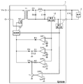
- FIG. 1 is a diagram for explaining a power supply device 1 according to a first embodiment of the present invention.
- the power supply device 1 is a DC-DC converter that supplies power to the load 2.
- a DC motor such as a linear motor is assumed as the load 2 in this specification.
- a large-capacitance capacitor C10 is externally connected in parallel with the DC motor. By charging the large-capacitance capacitor C10 at the time of startup, instantaneous power at the time of startup is ensured.
- the power supply device 1 includes a switching element M1, a transformer T1, a first diode D1, a second diode D2, an inductor L1, and a first capacitor C1 as a basic configuration of the switching regulator.
- a DC input voltage Vin is applied to the primary winding of the transformer T1.
- the switching element M1 is inserted between the input source of the input voltage Vin and the primary winding of the transformer T1, and conducts / cuts off between the two.
- FIG. 1 illustrates an example in which an N-channel MOSFET is used as the switching element M1, other switching elements such as an IGBT may be used.
- the output voltage of the secondary winding of the transformer T1 is rectified by a rectifier circuit including a first diode D1 and a second diode D2, and smoothed by a smoothing circuit including an inductor L1 and a first capacitor C1.
- FIG. 1 shows a forward DC-DC converter as an example of a switching regulator, but this is an example, and other switching regulators may be used.
- a flyback type DC-DC converter a push-pull type DC-DC converter, a bridge type DC-DC converter, or the like may be used.
- a non-insulating switching regulator that does not use a transformer may be used.
- the voltage detector 11 detects the output voltage of the switching regulator.
- the voltage detection unit 11 can be configured by an error amplifier, for example.
- the voltage detection unit 11 outputs the detected output voltage to the control unit 13.
- the current detector 12 detects the output current of the switching regulator.
- the current detection unit 12 can be configured by, for example, a shunt resistor and an error amplifier.
- the current detection unit 12 outputs a voltage corresponding to the output current of the switching regulator.
- the control unit 13 adaptively changes the duty ratio of the drive signal input to the control terminal (a gate terminal in the case of a MOSFET) of the switching element M1 according to the output voltage of the switching regulator detected by the voltage detection unit 11. .
- feedback control is applied so that the output voltage of the switching regulator is kept constant. Specifically, when the output voltage of the switching regulator is lower than the target voltage, the duty ratio of the switching element M1 is increased. Conversely, when the output voltage of the switching regulator is higher than the target voltage, the duty ratio of the switching element M1 is decreased.
- Embodiment 1 includes three types of overcurrent protection circuits, that is, a peak overcurrent protection circuit, an average overcurrent protection circuit, and a startup overcurrent protection circuit.
- a peak overcurrent protection circuit 10A
- the rated peak current 28A.
- a large amount of instantaneous power is used to drive the motor, and the switching regulator is designed to withstand a short peak current.
- 30A is set as the first overcurrent set value for activating the peak overcurrent protection circuit
- 11A is set as the second overcurrent set value for activating the overcurrent protection circuit for averaging
- the overcurrent for start-up is set.
- the third overcurrent set value that activates the protection circuit is 6A.
- the peak overcurrent protection circuit is realized by the first comparator CP1.
- the first comparator CP1 is composed of an operational amplifier, and the output voltage of the current detection unit 12 is input to the non-inverting input terminal, and the first reference voltage Vr1 corresponding to the first overcurrent setting value is input to the inverting input terminal.
- the first comparator CP1 outputs a high level when the voltage corresponding to the output current of the switching regulator input from the current detector 12 exceeds the first reference voltage Vr1, and outputs a low level when it does not exceed.
- the output voltage of the first comparator CP1 is output to the control unit 13 via the third diode D3.
- the control unit 13 limits the output current of the switching regulator by reducing the duty ratio of the drive signal input to the control terminal of the switching element M1 when the output voltage of the first comparator CP1 is at a high level.
- the peak overcurrent protection circuit instructs the control unit 13 to limit the output current of the switching regulator when the output current value of the switching regulator exceeds the first overcurrent set value.
- the average overcurrent protection circuit is realized by the second comparator CP2 and the low-pass filter.
- the second comparator CP2 is composed of an operational amplifier, and the output voltage of the current detector 12 is input to the non-inverting input terminal, and the second reference voltage Vr2 corresponding to the second overcurrent setting value is input to the inverting input terminal.
- the second comparator CP2 outputs a high level when the voltage corresponding to the output current of the switching regulator input from the current detection unit 12 exceeds the second reference voltage Vr2, and outputs a low level when the voltage does not exceed the second reference voltage Vr2.
- the low-pass filter composed of the first resistor R1 and the second capacitor C2 is connected to the output terminal of the second comparator CP2.
- the low-pass filter integrates the output voltage of the second comparator CP2.
- the output voltage of the second comparator CP2 integrated by the low-pass filter is output to the control unit 13 via the fourth diode D4.
- the power supply device 1 drives a DC motor with a pulse current
- the current during the on period of the pulse current exceeds the second overcurrent set value. Is also acceptable. This design condition is approximated by optimally setting the time constant of the low-pass filter and the second reference voltage Vr2. When the current during the ON period of the pulse current exceeds the first overcurrent set value, it is limited by the peak overcurrent protection circuit.
- the control unit 13 When the output voltage of the first comparator CP1 to which the low-pass filter characteristic is added is at a high level, the control unit 13 reduces the duty ratio of the drive signal input to the control terminal of the switching element M1 and limits the output current of the switching regulator. . As described above, the average overcurrent protection circuit instructs the control unit 13 to limit the output current of the switching regulator when the average value of the output current value of the switching regulator in a certain period exceeds the second overcurrent set value. To do.
- the overcurrent protection circuit for startup is realized by the third comparator CP3, the second resistor R2, the transistor Tr1, and the fourth comparator CP4.
- the third comparator CP3 is composed of an operational amplifier, and the output voltage of the current detection unit 12 is input to the non-inverting input terminal, and the third reference voltage Vr3 corresponding to the third overcurrent setting value is input to the inverting input terminal.
- the third comparator CP3 outputs a high level when the voltage corresponding to the output current of the switching regulator input from the current detection unit 12 exceeds the third reference voltage Vr3, and outputs a low level when the voltage does not exceed the third reference voltage Vr3.
- the output terminal of the third comparator CP3 is connected to the first node N1 via the second resistor R2.
- the transistor Tr1 is inserted between the first node N1 and a non-significant reference potential (ground potential in FIG. 1).
- the transistor Tr1 is an example of a switch, and other semiconductor switches or relays may be used.
- the fourth comparator CP4 is composed of an operational amplifier, and the output voltage of the voltage detector 11 is input to the non-inverting input terminal, and the fourth reference voltage Vr4 corresponding to the low voltage setting value is input to the inverting input terminal.
- the low voltage set value is set to a voltage of about 75 to 95% of the set drive voltage of the load 2.
- the output terminal of the fourth comparator CP4 is connected to the base terminal of the transistor Tr1.
- the fourth comparator CP4 outputs a high level when the output voltage of the switching regulator supplied to the load 2 exceeds the fourth reference voltage Vr4, and outputs a low level when it does not exceed the fourth reference voltage Vr4. While the output voltage of the fourth comparator CP4 is at a low level, the transistor Tr1 is in an off state, and the first node N1 and the ground are disconnected. When the output voltage of the fourth comparator CP4 transitions to a high level, the transistor Tr1 is turned on, and the potential of the first node N1 is fixed to the ground potential.
- the transistor Tr1 and the fourth comparator CP4 function as UVA (Under Voltage Alarm). That is, the output voltage of the third comparator CP3 is validated until the load voltage reaches the low voltage set value, and when the load voltage exceeds the low voltage set value, the output voltage of the third comparator CP3 is latched to the ground potential and invalidated.
- UVA Under Voltage Alarm
- the overcurrent protection circuit for start-up instructs the control unit 13 to limit the output current of the switching regulator when the output current value of the switching regulator exceeds the third overcurrent set value during start-up. After startup, the overcurrent protection circuit for startup is latched and stopped.
- FIG. 2 is a diagram showing a power supply device 1 according to a comparative example.
- the power supply device 1 according to the comparative example illustrated in FIG. 2 has a configuration that does not include the overcurrent protection circuit for startup, as compared with the power supply device 1 according to the first embodiment illustrated in FIG. Specifically, the third comparator CP3, the second resistor R2, the transistor Tr1, the fourth comparator CP4, and the fifth diode D5 are not provided.
- FIG. 3 is a timing chart for explaining the operation when the power supply device 1 is started.
- FIG. 3A is a timing chart showing transitions of the output current I and the output voltage V when the power supply device 1 according to the comparative example shown in FIG. 2 is started.
- FIG. 3B is a timing chart showing transitions of the output current I and the output voltage V when the power supply device 1 according to the first embodiment shown in FIG. 1 is started.
- the output current I gradually decreases.
- the larger the capacity of the large-capacitance capacitor C10 the longer the overcurrent operation time at startup and the greater the burden on the power supply device 1.
- a temperature alarm (not shown) may occur during charging of the large-capacitance capacitor C10, and the operation of the power supply device 1 may stop.
- an overcurrent protection circuit for startup that functions only at startup is added.
- the start-up overcurrent protection circuit charges the large-capacitance capacitor C10 with a constant current (CC charge) at a current value lower than the rated current value at the time of start-up.
- the output current I gradually decreases.
- the capacity of 75 to 95% of the large-capacitance capacitor C10 is charged with a constant current at the third overcurrent set value I1s lower than the rated current. Therefore, the charging time is slightly longer than that in FIG. 3A, but the burden on the power supply device 1 is greatly reduced.
- the startup overcurrent protection circuit is provided, so that the power supply device 1 can be started up. Can reduce stress. Therefore, it is possible to avoid the operation being stopped during the activation due to the temperature alarm.
- a plurality of power supply devices 1 may be connected in parallel and operated in parallel.
- the large-capacity capacitor C10 connected in parallel to the load 2 is charged with a small number of power supply devices 1.
- the charging time of the large-capacitance capacitor C10 becomes longer.
- the power supply device 1 according to the comparative example the time during which a current exceeding the rated current flows becomes long, and the stress on the power supply device 1 that is operating increases.
- the power supply device 1 according to the first embodiment even when the number of operating units is reduced, the charging time is extended, so that an increase in stress on the operating power supply device 1 can be suppressed.
- FIG. 4 is a diagram for explaining the power supply device 1 according to the second embodiment of the present invention.
- the power supply device 1 according to the second embodiment has a configuration in which one comparator is shared by the peak overcurrent protection circuit and the startup overcurrent protection circuit.
- the first comparator CP1 is shared by the peak overcurrent protection circuit and the startup overcurrent protection circuit.
- the third comparator CP3, the second resistor R2, and the fifth diode D5 shown in FIG. 1 are omitted.
- the voltage of the second node N2 is input to the inverting input terminal of the first comparator CP1.
- the voltage of the second node N2 is generated by dividing the reference voltage Vr0 higher than the first reference voltage Vr1 by the third resistor R3 and the fourth resistor R4.
- the divided voltage by the third resistor R3 and the fourth resistor R4 corresponds to the first reference voltage Vr1.
- the transistor Tr1 is inserted not between the first node N1 but the second node N2 and the ground.
- a fifth resistor R5 is inserted between the second node N2 and the transistor Tr1.
- Example 2 the output voltage of the voltage detector 11 is input to the inverting input terminal of the fourth comparator CP4, and the fourth reference voltage Vr4 corresponding to the low voltage setting value is input to the non-inverting input terminal.
- the fourth comparator CP4 outputs a low level when the output voltage of the switching regulator supplied to the load 2 exceeds the fourth reference voltage Vr4, and outputs a high level when not exceeding. While the output voltage of the fourth comparator CP4 is at the high level, the transistor Tr1 is in the on state, the second node N2 and the ground are in conduction, and the fifth resistor R5 is valid.
- the divided voltage by the third resistor R3, the fourth resistor R4, and the fifth resistor R5 corresponds to the third reference voltage Vr3.
- the third reference voltage Vr3 is input to the inverting input terminal of the first comparator CP1. That is, the first comparator CP1 functions as an overcurrent protection circuit for startup.
- the transistor Tr1 When the output voltage of the fourth comparator CP4 transitions to the low level, the transistor Tr1 is turned off, the second node N2 and the ground are disconnected, and the fifth resistor R5 is disabled. As a result, the potential of the second node N2 rises, and the first reference voltage Vr1 is input to the inverting input terminal of the first comparator CP1. Thus, in a state where the output voltage of the switching regulator exceeds the low voltage set value, the first reference voltage Vr1 is input to the inverting input terminal of the first comparator CP1. That is, the first comparator CP1 functions as a peak overcurrent protection circuit.
- the first comparator CP1 outputs a comparison result between the voltage corresponding to the output current value of the switching regulator and the third reference voltage Vr3 to the control unit 13 when the output voltage of the switching regulator is equal to or lower than the low voltage set value.
- the comparison result between the voltage corresponding to the output current value of the switching regulator and the first reference voltage Vr1 is output to the control unit 13.
- the same effects as the first embodiment are obtained. Compared with the first embodiment, the number of operational amplifiers used for overcurrent protection can be reduced.
- FIG. 5 is a diagram for explaining the power supply device 1 according to the third embodiment of the present invention.
- the overcurrent protection circuit for activation becomes invalid when the set time has elapsed since the activation, not when the load voltage exceeds the low voltage set value.
- a timer 14 is provided instead of the fourth comparator CP4 shown in FIG. The timer 14 turns on the transistor Tr1 when a set time elapses after the activation signal is input. The set time is set to a time corresponding to the charging time of the large-capacity capacitor C10.
- the third embodiment is effective when the capacity of the large-capacitance capacitor C10 to be used is fixed.
- the first and second embodiments are triggered not by time but by voltage, overcurrent protection at the time of start-up functions effectively regardless of the capacity of the large-capacity capacitor C10. Therefore, the highly versatile power supply device 1 can be configured.
- Example 1-3 described above an example is given in which the first overcurrent set value (30 A) is set to about 1.07 times the rated peak current value (28 A).
- the first overcurrent set value may be a value in the vicinity of the rated peak current value, and may be set within a range of about ⁇ 10% of the rated peak current value.
- the second overcurrent set value (11A) is set to 1.1 times the rated current value (10A).
- the second overcurrent set value may be a value in the vicinity of the rated current value, and may be set within a range of about ⁇ 20% of the rated current value.
- the present invention can be used in a power supply device that supplies electric power to a motor.
Landscapes
- Engineering & Computer Science (AREA)
- Power Engineering (AREA)
- Dc-Dc Converters (AREA)
- Emergency Protection Circuit Devices (AREA)
Abstract
第1過電流保護部は、電流検出部12により検出された電流値が、本電源装置1の定格電流値より高い値に設定された第1設定電流値を超えるとき、レギュレータの出力電流を制限するよう制御部13に指示する。第2過電流保護部は、電流検出部12により検出された電流値の一定期間における平均値が、定格電流値に対応する値に設定された第2設定電流値を超えたとき、レギュレータの出力電流を制限するよう制御部13に指示する。第3過電流保護部は、起動時において、電流検出部12により検出された電流値が、第2設定電流値より低い値に設定された第3設定電流値を超えるとき、レギュレータの出力電流を制限するよう制御部13に指示する。
Description
本発明は、モータ等の負荷に電力を供給する過電流保護付き電源装置に関する。
モータ負荷は大電力を必要とし、そのピーク電力は他の一般的な負荷に比べて大きくなる。そこで起動時の瞬時パワーを確保するため、モータと並列に大容量のコンデンサを接続することが多い。このコンデンサは起動時に充電され、モータの起動トルクを大きくする作用を担う。
DCモータはパルス状の電流で駆動されることも多い。パルス電流を出力可能な電源装置では一般的に、ピーク電力用の過電流保護と平均電力用の過電流保護の2つが実装される。前者はピーク電流を検出したとき出力を制御するものであり、後者は単位周期における平均電流が定格電流を超えたとき出力を制限するものである。後者の過電流保護は、瞬間的に定格電流を超える電流が流れても単位周期における平均電流が定格電流を超えない場合、発動されない。
特許文献1は、2段階の過電流検出値を設定可能な電源装置を開示する。当該電源装置では、負荷等の短絡に起因して出力電圧が異常となり、且つ定常状態信号が出力されているとき(即ち、起動時ではないとき)、過電流検出値として比較的小さな値を有する第1過電流検出値が設定される。また起動時には過電流検出値として比較的大きな値を有する第2過電流検出値が設定される。また出力電圧が正常であるとき(即ち、出力電圧が一定電圧以上に立ち上がっており、負荷に短絡等の異常が発生していないとき)、第2過電流検出値が設定される。
上述のように負荷と並列に大容量のコンデンサが接続される場合、起動時に電源装置から当該コンデンサに大電流が流れる。その際、上記ピーク電力用の過電流保護が発動する。その後、平均電力用の過電流保護が発動し、平均電力用の過電流保護の制限を受けながら電圧が立ち上がる。いずれの状態も定格電力以上を出力している状態であるため、熱ストレス等の負担が大きくなる。
本発明はこうした状況に鑑みてなされたものであり、その目的は、容量が大きい負荷に電力を供給する電源装置において起動時のストレスを軽減する技術を提供することにある。
上記課題を解決するために、本発明のある態様の過電流保護付き電源装置は、負荷に電力を供給するレギュレータと、前記レギュレータに含まれるスイッチング素子を制御する制御部と、前記レギュレータの出力電流を検出する電流検出部と、前記電流検出部により検出された電流値が、本電源装置の定格電流値より高い値に設定された第1設定電流値を超えるとき、前記レギュレータの出力電流を制限するよう前記制御部に指示する第1過電流保護部と、前記電流検出部により検出された電流値の一定期間における平均値が、定格電流値に対応する値に設定された第2設定電流値を超えたとき、前記レギュレータの出力電流を制限するよう前記制御部に指示する第2過電流保護部と、起動時において、前記電流検出部により検出された電流値が、前記第2設定電流値より低い値に設定された第3設定電流値を超えるとき、前記レギュレータの出力電流を制限するよう前記制御部に指示する第3過電流保護部と、を備える。
本発明によれば、容量が大きい負荷に電力を供給する電源装置において起動時のストレスを軽減できる。
図1は、本発明の実施例1に係る電源装置1を説明するための図である。電源装置1は負荷2に電力を供給するDC-DCコンバータである。以下、本明細書では負荷2として、リニアモータ等のDCモータを想定する。一般にDCモータでは起動トルクを確保するため、DCモータと並列に大容量コンデンサC10が外付けされる。起動時に大容量コンデンサC10に充電することにより、起動時の瞬時パワーが確保される。
電源装置1はスイッチングレギュレータの基本構成として、スイッチング素子M1、トランスT1、第1ダイオードD1、第2ダイオードD2、インダクタL1及び第1コンデンサC1を含む。トランスT1の一次巻線に直流の入力電圧Vinが印加される。スイッチング素子M1は、当該入力電圧Vinの入力源とトランスT1の一次巻線との間に挿入され、両者の間を導通/遮断する。図1ではスイッチング素子M1としてNチャンネルMOSFETを使用する例を描いているが、IGBT等の他のスイッチング素子を用いてもよい。トランスT1の二次巻線の出力電圧は、第1ダイオードD1及び第2ダイオードD2で構成される整流回路で整流され、インダクタL1及び第1コンデンサC1で構成される平滑回路により平滑化される。
図1ではスイッチングレギュレータの一例として、フォワード型DC-DCコンバータを描いているが一例であり、他のスイッチングレギュレータを使用してもよい。例えばフライバック型DC-DCコンバータ、プッシュプル型DC-DCコンバータ、ブリッジ型DC-DCコンバータ等を使用してもよい。またトランスを用いない非絶縁型のスイッチングレギュレータを使用してもよい。
電圧検出部11は、スイッチングレギュレータの出力電圧を検出する。電圧検出部11は例えばエラーアンプで構成できる。電圧検出部11は検出した出力電圧を制御部13に出力する。電流検出部12はスイッチングレギュレータの出力電流を検出する。電流検出部12は例えば、シャント抵抗とエラーアンプにより構成できる。電流検出部12はスイッチングレギュレータの出力電流に対応する電圧を出力する。
制御部13は、電圧検出部11で検出されたスイッチングレギュレータの出力電圧に応じて、スイッチング素子M1の制御端子(MOSFETの場合、ゲート端子)に入力する駆動信号のデューティ比を適応的に変化させる。これによりスイッチングレギュレータの出力電圧が一定に保たれるようフィードバック制御がかかる。具体的にはスイッチングレギュレータの出力電圧が目標電圧より低い場合はスイッチング素子M1のデューティ比を上げ、反対にスイッチングレギュレータの出力電圧が目標電圧より高い場合はスイッチング素子M1のデューティ比を下げる。
実施例1では3種類の過電流保護回路、即ち、ピーク用の過電流保護回路、平均用の過電流保護回路および起動時用の過電流保護回路を備える。以下の説明では、スイッチングレギュレータの定格電流を10Aとし、定格ピーク電流を28Aとする例を想定する。モータを駆動するために瞬時大電力を使用する場合があり、当該スイッチングレギュレータは短時間のピーク電流に耐えられる仕様になっている。また以下の説明では、ピーク用の過電流保護回路が発動する第1過電流設定値として30A、平均用の過電流保護回路が発動する第2過電流設定値として11A、起動時用の過電流保護回路が発動する第3過電流設定値として6Aとする例を想定する。
図1において、ピーク用の過電流保護回路は第1コンパレータCP1により実現される。第1コンパレータCP1はオペアンプで構成され、その非反転入力端子に電流検出部12の出力電圧が入力され、反転入力端子に第1過電流設定値に対応する第1参照電圧Vr1が入力される。第1コンパレータCP1は、電流検出部12から入力されるスイッチングレギュレータの出力電流に対応する電圧が第1参照電圧Vr1を超えるときハイレベルを出力し、超えないときローレベルを出力する。第1コンパレータCP1の出力電圧は第3ダイオードD3を介して制御部13に出力される。
制御部13は第1コンパレータCP1の出力電圧がハイレベルのとき、スイッチング素子M1の制御端子に入力する駆動信号のデューティ比を下げてスイッチングレギュレータの出力電流を制限する。このようにピーク用の過電流保護回路は、スイッチングレギュレータの出力電流値が第1過電流設定値を超えるとき、スイッチングレギュレータの出力電流を制限するよう制御部13に指示する。
平均用の過電流保護回路は第2コンパレータCP2及びローパスフィルタにより実現される。第2コンパレータCP2はオペアンプで構成され、その非反転入力端子に電流検出部12の出力電圧が入力され、反転入力端子に第2過電流設定値に対応する第2参照電圧Vr2が入力される。第2コンパレータCP2は、電流検出部12から入力されるスイッチングレギュレータの出力電流に対応する電圧が第2参照電圧Vr2を超えたときハイレベルを出力し、超えないときローレベルを出力する。
第2コンパレータCP2の出力端子に、第1抵抗R1及び第2コンデンサC2で構成されるローパスフィルタが接続される。ローパスフィルタは第2コンパレータCP2の出力電圧を積分する。ローパスフィルタにより積分された第2コンパレータCP2の出力電圧は第4ダイオードD4を介して制御部13に出力される。
電源装置1がパルス電流でDCモータを駆動する場合、単位周期あたりの平均電流が第2過電流設定値以下であれば、パルス電流のオン期間の電流が第2過電流設定値を超えていても許容される。この設計条件を、ローパスフィルタの時定数と第2参照電圧Vr2を最適に設定することにより近似する。なおパルス電流のオン期間の電流が第1過電流設定値を超えている場合は、ピーク用の過電流保護回路により制限される。
制御部13は、ローパスフィルタ特性が付加された第1コンパレータCP1の出力電圧がハイレベルのとき、スイッチング素子M1の制御端子に入力する駆動信号のデューティ比を下げてスイッチングレギュレータの出力電流を制限する。このように平均用の過電流保護回路は、スイッチングレギュレータの出力電流値の一定期間における平均値が第2過電流設定値を超えたとき、スイッチングレギュレータの出力電流を制限するよう制御部13に指示する。
起動時用の過電流保護回路は第3コンパレータCP3、第2抵抗R2、トランジスタTr1及び第4コンパレータCP4により実現される。第3コンパレータCP3はオペアンプで構成され、その非反転入力端子に電流検出部12の出力電圧が入力され、反転入力端子に第3過電流設定値に対応する第3参照電圧Vr3が入力される。第3コンパレータCP3は、電流検出部12から入力されるスイッチングレギュレータの出力電流に対応する電圧が第3参照電圧Vr3を超えたときハイレベルを出力し、超えないときローレベルを出力する。
第3コンパレータCP3の出力端子は第2抵抗R2を介して第1ノードN1に接続される。第1ノードN1と、非有意な基準電位(図1ではグラウンド電位)との間にトランジスタTr1が挿入される。なおトランジスタTr1はスイッチの一例であり、他の半導体スイッチを用いてもよいし、リレーを用いてもよい。
第4コンパレータCP4はオペアンプで構成され、その非反転入力端子に電圧検出部11の出力電圧が入力され、反転入力端子に低電圧設定値に対応する第4参照電圧Vr4が入力される。低電圧設定値は、負荷2の設定駆動電圧の75~95%程度の電圧に設定される。第4コンパレータCP4の出力端子はトランジスタTr1のベース端子に接続される。
第4コンパレータCP4は、負荷2に供給されているスイッチングレギュレータの出力電圧が第4参照電圧Vr4を超えたときハイレベルを出力し、超えないときローレベルを出力する。第4コンパレータCP4の出力電圧がローレベルの間、トランジスタTr1はオフ状態であり、第1ノードN1とグラウンドは切り離される。第4コンパレータCP4の出力電圧がハイレベルに遷移するとトランジスタTr1はターンオンし、第1ノードN1の電位をグラウンド電位に固定する。
このようにトランジスタTr1及び第4コンパレータCP4はUVA(Under Voltage Alarm)として機能する。即ち負荷電圧が低電圧設定値に到達するまで、第3コンパレータCP3の出力電圧を有効化し、低電圧設定値を超えると第3コンパレータCP3の出力電圧をグラウンド電位にラッチして無効化する。
スイッチングレギュレータの出力電圧が低電圧設定値以下の場合、第1コンパレータCP1の出力電圧が第5ダイオードD5を介してそのまま制御部13に出力される。スイッチングレギュレータの出力電圧が低電圧設定値を超える場合、常にローレベルが制御部13に出力される。このように起動時用の過電流保護回路は起動時において、スイッチングレギュレータの出力電流値が第3過電流設定値を超えたとき、スイッチングレギュレータの出力電流を制限するよう制御部13に指示する。起動後は起動時用の過電流保護回路はラッチ停止される。
図2は、比較例に係る電源装置1を示す図である。図2に示す比較例に係る電源装置1は、図1に示した実施例1に係る電源装置1と比較して、起動時用の過電流保護回路を備えない構成である。具体的には第3コンパレータCP3、第2抵抗R2、トランジスタTr1、第4コンパレータCP4及び第5ダイオードD5を備えない構成である。
図3は、電源装置1の起動時の動作を説明するためのタイミングチャートである。図3(a)は図2に示した比較例に係る電源装置1の起動時における出力電流I及び出力電圧Vの推移を示すタイミングチャートである。図3(b)は図1に示した実施例1に係る電源装置1の起動時における出力電流I及び出力電圧Vの推移を示すタイミングチャートである。
図3(a)において、電源装置1が起動すると電源装置1の出力電流Iで大容量コンデンサC10の充電が開始される。出力電流Iが第1過電流設定値I1pに到達すると、ピーク用の過電流保護回路により出力電流Iが第1過電流設定値I1p以下に制限されながら出力電圧Vが上昇する。ピーク用の過電流保護回路は時間規定(例えば100ms)の範囲内で動作する。その時間規定を超えると平均用の過電流保護回路により出力電流Iが第2過電流設定値I2a以下に制限されながら出力電圧Vが上昇する。
大容量コンデンサC10の充電が終了し、出力電圧Vが負荷2の設定駆動電圧Vdに到達すると出力電流Iが徐々に低下する。この起動シーケンスでは、大容量コンデンサC10の容量が大きくなるほど、起動時に過電流動作する時間が長くなり電源装置1の負担が大きくなる。例えば大容量コンデンサC10への充電途中で温度アラーム(不図示)が発生し、電源装置1の動作が停止してしまう場合も発生し得る。
これに対して実施例1では、起動時だけ機能する起動時用の過電流保護回路が追加されている。起動時用の過電流保護回路は起動時において、定格電流値より低い電流値で大容量コンデンサC10を定電流充電(CC充電)する。
図3(b)において、電源装置1が起動すると電源装置1の出力電流Iで大容量コンデンサC10の充電が開始される。出力電流Iが第3過電流設定値I3sに到達すると、起動時用の過電流保護回路により第3過電流設定値I1sで大容量コンデンサC10が定電流充電される。出力電圧Vが低電圧設定値Vuに到達すると、起動時用の過電流保護回路がラッチ停止する。起動時用の過電流保護回路がラッチ停止すると、平均用の過電流保護回路により出力電流Iが第2過電流設定値I2a以下に制限されながら出力電圧Vが上昇する。
大容量コンデンサC10の充電が終了し、出力電圧Vが負荷2の設定駆動電圧Vdに到達すると出力電流Iが徐々に低下する。この起動シーケンスでは、大容量コンデンサC10の75~95%の容量が、定格電流より低い第3過電流設定値I1sで定電流充電される。従って図3(a)と比較して充電時間が若干長くなるが、電源装置1の負担が大幅に軽減される。
以上説明したように実施例1によれば、ピーク用の過電流保護回路および平均用の過電流保護回路に加えて、起動時用の過電流保護回路を設けることにより、電源装置1における起動時のストレスを軽減できる。従って温度アラームにより起動途中で動作が停止してしまうことも回避できる。
大電力が必要な負荷2の場合、複数の電源装置1を並列接続して並列運転することがある。複数の電源装置1の内、故障などにより運転台数が減った場合、負荷2に並列接続される大容量コンデンサC10を少ない数の電源装置1で充電することになる。この場合、出力電流が低下しているため大容量コンデンサC10の充電時間が長くなる。比較例に係る電源装置1を使用している場合、定格電流を超える電流が流れる時間が長くなり、稼働している電源装置1へのストレスが大きくなる。これに対して実施例1に係る電源装置1を使用している場合、運転台数が減った場合でも充電時間の延長で対応するため、稼働している電源装置1へのストレス増加を抑制できる。
図4は、本発明の実施例2に係る電源装置1を説明するための図である。実施例2に係る電源装置1は、1つのコンパレータをピーク用の過電流保護回路と起動時用の過電流保護回路で共有する構成である。図4に示すように第1コンパレータCP1がピーク用の過電流保護回路と起動時用の過電流保護回路で共有される。図4に示す電源装置1では、図1に示した第3コンパレータCP3、第2抵抗R2及び第5ダイオードD5は省略される。
第1コンパレータCP1の反転入力端子には、第2ノードN2の電圧が入力される。第2ノードN2の電圧は、第1参照電圧Vr1より高い参照電圧Vr0を、第3抵抗R3と第4抵抗R4で分圧して生成される。第3抵抗R3と第4抵抗R4による分圧電圧は第1参照電圧Vr1に対応する。実施例2ではトランジスタTr1は、第1ノードN1ではなく第2ノードN2と、グラウンドとの間に挿入される。第2ノードN2とトランジスタTr1との間には第5抵抗R5が挿入される。
実施例2では第4コンパレータCP4の反転入力端子に電圧検出部11の出力電圧が入力され、非反転入力端子に低電圧設定値に対応する第4参照電圧Vr4が入力される。第4コンパレータCP4は、負荷2に供給されているスイッチングレギュレータの出力電圧が第4参照電圧Vr4を超えたときローレベルを出力し、超えないときハイレベルを出力する。第4コンパレータCP4の出力電圧がハイレベルの間、トランジスタTr1はオン状態であり、第2ノードN2とグラウンドが導通しており、第5抵抗R5は有効である。第3抵抗R3と、第4抵抗R4及び第5抵抗R5による分圧電圧は第3参照電圧Vr3に対応する。従ってスイッチングレギュレータの出力電圧が低電圧設定値以下の状態では、第1コンパレータCP1の反転入力端子に第3参照電圧Vr3が入力される。即ち第1コンパレータCP1は起動時用の過電流保護回路として機能する。
第4コンパレータCP4の出力電圧がローレベルに遷移するとトランジスタTr1はターンオフし、第2ノードN2とグラウンドは切り離され、第5抵抗R5は無効になる。これにより第2ノードN2の電位が上昇し、第1コンパレータCP1の反転入力端子に第1参照電圧Vr1が入力されるようになる。このようにスイッチングレギュレータの出力電圧が低電圧設定値を超えている状態では、第1コンパレータCP1の反転入力端子に第1参照電圧Vr1が入力される。即ち第1コンパレータCP1はピーク用の過電流保護回路として機能する。
第1コンパレータCP1は、スイッチングレギュレータの出力電圧が低電圧設定値以下のとき、スイッチングレギュレータの出力電流値に対応する電圧と第3参照電圧Vr3との比較結果を制御部13に出力する。スイッチングレギュレータの出力電圧が低電圧設定値を超えるとき、スイッチングレギュレータの出力電流値に対応する電圧と第1参照電圧Vr1との比較結果を制御部13に出力する。
以上説明したように実施例2によれば、実施例1と同様の効果を奏する。実施例1と比較して過電流保護に使用するオペアンプの数を削減できる。
図5は、本発明の実施例3に係る電源装置1を説明するための図である。実施例3に係る電源装置1では起動用の過電流保護回路は、負荷電圧が低電圧設定値を超えたときではなく、起動から設定時間が経過したとき無効になる。図5に示す電源装置1では、図1に示した第4コンパレータCP4の代わりにタイマ14が設けられる。タイマ14は、起動信号が入力されてから設定時間が経過するとトランジスタTr1をターンオンする。設定時間は大容量コンデンサC10の充電時間に対応した時間に設定される。
以上説明したように実施例3によれば、実施例1、2と同様の効果を奏する。実施例3は、使用する大容量コンデンサC10の容量が固定の場合に有効である。一方、実施例1、2は、時間ではなく電圧をトリガとするため大容量コンデンサC10の容量に関係なく起動時の過電流保護が有効に機能する。従って汎用性の高い電源装置1を構成できる。
以上、本発明を実施例1-3をもとに説明した。これらの実施例は例示であり、それらの各構成要素や各処理プロセスの組合せにいろいろな変形例が可能なこと、またそうした変形例も本発明の範囲にあることは当業者に理解されるところである。
上述の実施例1-3では、第1過電流設定値(30A)を定格ピーク電流値(28A)の約1.07倍に設定する例を挙げた。この点、第1過電流設定値は定格ピーク電流値の近傍の値であればよく定格ピーク電流値の±10%程度の範囲内に設定されればよい。また上述の実施例1-3では、第2過電流設定値(11A)を定格電流値(10A)の1.1倍に設定する例を挙げた。この点、第2過電流設定値は定格電流値の近傍の値であればよく定格電流値の±20%程度の範囲内に設定されればよい。
また上述の説明では、3段階の過電流保護をスイッチングレギュレータに適用する例を説明したが、リニアレギュレータにも適用可能である。
1 電源装置、 2 負荷、 M1 スイッチング素子、 T1 トランス、 L1 インダクタ、 C1 第1コンデンサ、 C2 第2コンデンサ、 C10 大容量コンデンサ、 CP1 第1コンパレータ、 CP2 第2コンパレータ、 CP3 第3コンパレータ、 CP4 第4コンパレータ、 D1 第1ダイオード、 D2 第2ダイオード、 D3 第3ダイオード、 D4 第4ダイオード、 D5 第5ダイオード、 R1 第1抵抗、 R2 第2抵抗、 R3 第3抵抗、 R4 第4抵抗、 R5 第5抵抗、 Tr1 トランジスタ、 11 電圧検出部、 12 電流検出部、 13 制御部、 14 タイマ。
本発明は、モータに電力を供給する電源装置に利用可能である。
Claims (5)
- 負荷に電力を供給するレギュレータと、
前記レギュレータに含まれるスイッチング素子を制御する制御部と、
前記レギュレータの出力電流を検出する電流検出部と、
前記電流検出部により検出された電流値が、本電源装置の定格電流値より高い値に設定された第1設定電流値を超えるとき、前記レギュレータの出力電流を制限するよう前記制御部に指示する第1過電流保護部と、
前記電流検出部により検出された電流値の一定期間における平均値が、定格電流値に対応する値に設定された第2設定電流値を超えたとき、前記レギュレータの出力電流を制限するよう前記制御部に指示する第2過電流保護部と、
起動時において、前記電流検出部により検出された電流値が、前記第2設定電流値より低い値に設定された第3設定電流値を超えるとき、前記レギュレータの出力電流を制限するよう前記制御部に指示する第3過電流保護部と、
を備えることを特徴とする過電流保護付き電源装置。 - 前記第3過電流保護部は、起動後において前記負荷の電圧が設定電圧値を超えると無効になることを特徴とする請求項1に記載の過電流保護付き電源装置。
- 前記第3過電流保護部は、
前記電流検出部により検出された電流値に対応する電圧と、前記第3設定電流値に対応する参照電圧との比較結果を前記制御部に出力するコンパレータと、
前記コンパレータの出力端子と、非有意な基準電位との間に挿入されるスイッチと、
を有し、
前記スイッチは、前記負荷の電圧が前記設定電圧値を超えたときターンオンすることを特徴とする請求項2に記載の過電流保護付き電源装置。 - 前記第1過電流保護部および前記第3過電流保護部は、
共有するコンパレータを有し、
前記コンパレータは、
前記負荷の電圧が前記設定電圧値以下のとき、前記電流検出部により検出された電流値に対応する電圧と、前記第3設定電流値に対応する第3参照電圧との比較結果を前記制御部に出力し、前記負荷の電圧が前記設定電圧値を超えるとき、前記電流検出部により検出された電流値に対応する電圧と、前記第1設定電流値に対応する第1参照電圧との比較結果を前記制御部に出力することを特徴とする請求項2に記載の過電流保護付き電源装置。 - 前記第3過電流保護部は、起動から設定時間が経過すると無効になることを特徴とする請求項1に記載の過電流保護付き電源装置。
Priority Applications (3)
| Application Number | Priority Date | Filing Date | Title |
|---|---|---|---|
| CN201680018702.XA CN107360734B (zh) | 2015-04-20 | 2016-04-18 | 带过流保护的电源装置 |
| KR1020177032868A KR102448640B1 (ko) | 2015-04-20 | 2016-04-18 | 과전류 보호 기능을 갖는 전원 장치 |
| US15/789,392 US10075061B2 (en) | 2015-04-20 | 2017-10-20 | Power supply device with excess current protection |
Applications Claiming Priority (2)
| Application Number | Priority Date | Filing Date | Title |
|---|---|---|---|
| JP2015-085725 | 2015-04-20 | ||
| JP2015085725A JP6326002B2 (ja) | 2015-04-20 | 2015-04-20 | 過電流保護付き電源装置 |
Related Child Applications (1)
| Application Number | Title | Priority Date | Filing Date |
|---|---|---|---|
| US15/789,392 Continuation US10075061B2 (en) | 2015-04-20 | 2017-10-20 | Power supply device with excess current protection |
Publications (1)
| Publication Number | Publication Date |
|---|---|
| WO2016171098A1 true WO2016171098A1 (ja) | 2016-10-27 |
Family
ID=57143861
Family Applications (1)
| Application Number | Title | Priority Date | Filing Date |
|---|---|---|---|
| PCT/JP2016/062234 Ceased WO2016171098A1 (ja) | 2015-04-20 | 2016-04-18 | 過電流保護付き電源装置 |
Country Status (5)
| Country | Link |
|---|---|
| US (1) | US10075061B2 (ja) |
| JP (1) | JP6326002B2 (ja) |
| KR (1) | KR102448640B1 (ja) |
| CN (1) | CN107360734B (ja) |
| WO (1) | WO2016171098A1 (ja) |
Cited By (1)
| Publication number | Priority date | Publication date | Assignee | Title |
|---|---|---|---|---|
| WO2025247820A1 (de) * | 2024-05-27 | 2025-12-04 | Siemens Aktiengesellschaft | Vorrichtung, anordnung und verfahren zur eigensicheren stromversorgung eines gerätes, sowie eigensicheres gerät |
Families Citing this family (8)
| Publication number | Priority date | Publication date | Assignee | Title |
|---|---|---|---|---|
| JP6761357B2 (ja) * | 2017-01-20 | 2020-09-23 | コーセル株式会社 | スイッチング電源装置 |
| CN110707764B (zh) * | 2019-10-31 | 2021-12-07 | 国家电网有限公司 | 用于opgw监测的感应取电系统 |
| CN114902511B (zh) * | 2019-12-25 | 2026-03-10 | 夏普Nec显示器解决方案株式会社 | 电力控制装置、显示装置、电力控制方法 |
| CN114337288A (zh) | 2020-09-29 | 2022-04-12 | 万国半导体国际有限合伙公司 | 具有恒压模式和恒流模式的隔离转换器及其控制方法 |
| TWI760867B (zh) * | 2020-09-29 | 2022-04-11 | 加拿大商萬國半導體國際有限合夥公司 | 具有恆壓模式和恆流模式的隔離轉換器及其控制方法 |
| CN115606090B (zh) | 2021-01-15 | 2025-08-29 | 华为数字能源技术有限公司 | 一种电机驱动方法、装置及系统 |
| DE102021126399A1 (de) * | 2021-10-12 | 2023-04-13 | WAGO Verwaltungsgesellschaft mit beschränkter Haftung | Verfahren und Schaltungsanordnung zur Regelung eines Schaltnetzteils |
| TWI907907B (zh) * | 2023-12-27 | 2025-12-11 | 致茂電子股份有限公司 | 定功率適應性限電流保護電路及定功率適應性限電流保護方法 |
Citations (3)
| Publication number | Priority date | Publication date | Assignee | Title |
|---|---|---|---|---|
| JP2001119933A (ja) * | 1999-10-19 | 2001-04-27 | Fujitsu Denso Ltd | 過電流保護回路 |
| JP2001345688A (ja) * | 2000-03-31 | 2001-12-14 | Denso Corp | 半導体スイッチング素子駆動回路 |
| JP2011160517A (ja) * | 2010-01-29 | 2011-08-18 | Panasonic Electric Works Co Ltd | 過電流保護回路、及びスイッチング電源装置 |
Family Cites Families (5)
| Publication number | Priority date | Publication date | Assignee | Title |
|---|---|---|---|---|
| JP2005073354A (ja) | 2003-08-22 | 2005-03-17 | Omron Corp | 電源 |
| JP2005323413A (ja) * | 2004-05-06 | 2005-11-17 | Rohm Co Ltd | 過電流検出回路及びこれを有する電源装置 |
| CN101141094B (zh) * | 2007-08-17 | 2010-12-08 | 浙江大学 | 限流滑模控制降压直流-直流变换器的控制方法及其控制器 |
| KR100916666B1 (ko) * | 2007-09-18 | 2009-09-08 | 엘지전자 주식회사 | 공기조화기 |
| US9143033B2 (en) * | 2010-11-30 | 2015-09-22 | Taiwan Semiconductor Manufacturing Company, Ltd. | Hysteretic power converter with calibration circuit |
-
2015
- 2015-04-20 JP JP2015085725A patent/JP6326002B2/ja active Active
-
2016
- 2016-04-18 CN CN201680018702.XA patent/CN107360734B/zh active Active
- 2016-04-18 WO PCT/JP2016/062234 patent/WO2016171098A1/ja not_active Ceased
- 2016-04-18 KR KR1020177032868A patent/KR102448640B1/ko active Active
-
2017
- 2017-10-20 US US15/789,392 patent/US10075061B2/en active Active
Patent Citations (3)
| Publication number | Priority date | Publication date | Assignee | Title |
|---|---|---|---|---|
| JP2001119933A (ja) * | 1999-10-19 | 2001-04-27 | Fujitsu Denso Ltd | 過電流保護回路 |
| JP2001345688A (ja) * | 2000-03-31 | 2001-12-14 | Denso Corp | 半導体スイッチング素子駆動回路 |
| JP2011160517A (ja) * | 2010-01-29 | 2011-08-18 | Panasonic Electric Works Co Ltd | 過電流保護回路、及びスイッチング電源装置 |
Cited By (1)
| Publication number | Priority date | Publication date | Assignee | Title |
|---|---|---|---|---|
| WO2025247820A1 (de) * | 2024-05-27 | 2025-12-04 | Siemens Aktiengesellschaft | Vorrichtung, anordnung und verfahren zur eigensicheren stromversorgung eines gerätes, sowie eigensicheres gerät |
Also Published As
| Publication number | Publication date |
|---|---|
| US10075061B2 (en) | 2018-09-11 |
| US20180041112A1 (en) | 2018-02-08 |
| CN107360734A (zh) | 2017-11-17 |
| KR102448640B1 (ko) | 2022-09-28 |
| JP2016208614A (ja) | 2016-12-08 |
| JP6326002B2 (ja) | 2018-05-16 |
| KR20170139065A (ko) | 2017-12-18 |
| CN107360734B (zh) | 2019-09-24 |
Similar Documents
| Publication | Publication Date | Title |
|---|---|---|
| JP6326002B2 (ja) | 過電流保護付き電源装置 | |
| US8018694B1 (en) | Over-current protection for a power converter | |
| US10530256B1 (en) | Multi-level buck converter with reverse charge capability | |
| JP2012060714A (ja) | 集積回路 | |
| JP5910395B2 (ja) | ドライブ回路 | |
| TWI420964B (zh) | 驅動電路及發光二極體驅動控制器 | |
| JP2017127109A (ja) | スイッチング電源装置 | |
| JP2012120267A (ja) | 充電制御装置 | |
| JP6171724B2 (ja) | Led電源装置及びled照明装置 | |
| US20130069564A1 (en) | Power controller | |
| JP6698631B2 (ja) | 電力変換装置およびその制御方法 | |
| WO2018042937A1 (ja) | スイッチング電源装置および半導体装置 | |
| US9780690B2 (en) | Resonant decoupled auxiliary supply for a switched-mode power supply controller | |
| TW201739156A (zh) | Dcdc轉換器 | |
| US9484801B2 (en) | Start-up regulator for high-input-voltage power converters | |
| JP2009195073A (ja) | スイッチング電源装置 | |
| JP2011062041A (ja) | スイッチング制御回路およびスイッチング電源回路 | |
| US8593830B2 (en) | Reverse current limit protection for active clamp converters | |
| JP2012105505A (ja) | 制御回路 | |
| US10333400B2 (en) | Boost DC-DC converter including a switching element | |
| EP3127228B1 (en) | Dc/dc converter and method of driving dc/dc converter | |
| JP7388939B2 (ja) | スイッチング電源 | |
| JP6371226B2 (ja) | 逆電流保護付きスイッチング電源装置 | |
| JP5926927B2 (ja) | スイッチングレギュレータ | |
| JP2020188670A (ja) | 電源制御装置、昇圧型dc/dcコンバータ、および降圧型dc/dcコンバータ |
Legal Events
| Date | Code | Title | Description |
|---|---|---|---|
| 121 | Ep: the epo has been informed by wipo that ep was designated in this application |
Ref document number: 16783119 Country of ref document: EP Kind code of ref document: A1 |
|
| NENP | Non-entry into the national phase |
Ref country code: DE |
|
| ENP | Entry into the national phase |
Ref document number: 20177032868 Country of ref document: KR Kind code of ref document: A |
|
| 122 | Ep: pct application non-entry in european phase |
Ref document number: 16783119 Country of ref document: EP Kind code of ref document: A1 |