WO2016170801A1 - 光トランシーバ、光通信装置、および受光素子の制御方法 - Google Patents
光トランシーバ、光通信装置、および受光素子の制御方法 Download PDFInfo
- Publication number
- WO2016170801A1 WO2016170801A1 PCT/JP2016/050087 JP2016050087W WO2016170801A1 WO 2016170801 A1 WO2016170801 A1 WO 2016170801A1 JP 2016050087 W JP2016050087 W JP 2016050087W WO 2016170801 A1 WO2016170801 A1 WO 2016170801A1
- Authority
- WO
- WIPO (PCT)
- Prior art keywords
- temperature
- temperature sensor
- bias voltage
- transmission
- light receiving
- Prior art date
- Legal status (The legal status is an assumption and is not a legal conclusion. Google has not performed a legal analysis and makes no representation as to the accuracy of the status listed.)
- Ceased
Links
Images





Classifications
-
- H—ELECTRICITY
- H04—ELECTRIC COMMUNICATION TECHNIQUE
- H04B—TRANSMISSION
- H04B10/00—Transmission systems employing electromagnetic waves other than radio-waves, e.g. infrared, visible or ultraviolet light, or employing corpuscular radiation, e.g. quantum communication
- H04B10/50—Transmitters
- H04B10/58—Compensation for non-linear transmitter output
-
- H—ELECTRICITY
- H04—ELECTRIC COMMUNICATION TECHNIQUE
- H04B—TRANSMISSION
- H04B10/00—Transmission systems employing electromagnetic waves other than radio-waves, e.g. infrared, visible or ultraviolet light, or employing corpuscular radiation, e.g. quantum communication
- H04B10/40—Transceivers
-
- H—ELECTRICITY
- H04—ELECTRIC COMMUNICATION TECHNIQUE
- H04B—TRANSMISSION
- H04B10/00—Transmission systems employing electromagnetic waves other than radio-waves, e.g. infrared, visible or ultraviolet light, or employing corpuscular radiation, e.g. quantum communication
- H04B10/50—Transmitters
- H04B10/501—Structural aspects
- H04B10/503—Laser transmitters
- H04B10/504—Laser transmitters using direct modulation
-
- H—ELECTRICITY
- H04—ELECTRIC COMMUNICATION TECHNIQUE
- H04B—TRANSMISSION
- H04B10/00—Transmission systems employing electromagnetic waves other than radio-waves, e.g. infrared, visible or ultraviolet light, or employing corpuscular radiation, e.g. quantum communication
- H04B10/60—Receivers
- H04B10/66—Non-coherent receivers, e.g. using direct detection
- H04B10/69—Electrical arrangements in the receiver
- H04B10/691—Arrangements for optimizing the photodetector in the receiver
- H04B10/6911—Photodiode bias control, e.g. for compensating temperature variations
Definitions
- the present invention relates to an optical transceiver, an optical communication device, and a method for controlling a light receiving element, and more particularly, to an optical transceiver including a light emitting element and a light receiving element, an optical communication device, and a method for controlling the light receiving element.
- ADSL Asymmetric Digital Subscriber Line
- FTTH Fiber To The Home
- ONU Optical Network Unit
- OHT Optical Line Terminal
- EPON Ethernet (registered trademark) PON
- MPCP Multi-Point Control Protocol
- OAM Operations Administration and Maintenance
- Non-Patent Document 1 describes a registration method for a new home device, a report indicating a bandwidth allocation request, and a gate indicating a transmission instruction using an MPCP message.
- GE-PON Giga Bit Ethernet (registered trademark) Passive Optical Network
- IEEE 802.3av registered trademark
- an avalanche photodiode (APD) having high light receiving sensitivity is used as a light receiving element.
- the APD is a light receiving element having a current amplifying function.
- the APD has a reverse bias voltage applied to the APD at the temperature of the APD. It is necessary to adjust accordingly.
- Patent Document 1 discloses the following configuration. That is, an optical transceiver integrated with a transmitter and receiver for transmitting and receiving an optical signal, which includes an optical transmission subassembly including a laser diode, an optical reception subassembly including an avalanche photodiode, and a temperature sensor. A first control circuit for driving the laser diode based on an output signal; and a second control circuit for controlling a bias voltage of the avalanche photodiode. The second control circuit controls the bias voltage based on a temperature correction value obtained by adding a predetermined offset value to the output of the temperature sensor.
- IEEE Std 802.3ah registered trademark
- feedforward control is performed using a temperature sensor and a lookup table related to the temperature in the optical transceiver.
- the detected temperature of the temperature sensor also fluctuates.
- the present invention has been made to solve the above-described problems, and an object of the present invention is to provide an optical transceiver, an optical communication apparatus, and a light receiving element control method capable of satisfactorily adjusting a bias voltage to the light receiving element. Is to provide.
- an optical transceiver includes a temperature sensor, an integrated circuit capable of performing arithmetic processing using a temperature detected by the temperature sensor, a light emitting element, and a light receiving element.
- An optical module a transmission driver that drives the light emitting element, a housing that houses the temperature sensor, the integrated circuit, the optical module, and the transmission driver, and that has thermal conductivity.
- the difference between the detected temperature of the temperature sensor in the signal transmission on state and the detected temperature of the temperature sensor in the optical signal transmission off state is greater than 2 ° C.
- the power consumption of the transmission driver is the power consumption of the integrated circuit And greater than the power consumption of the optical module.
- an optical transceiver includes a first temperature sensor, a second temperature sensor, an optical module including a light emitting element and a light receiving element, and the second temperature sensor.
- the driving rate of the transmission driver is a, the detected temperature of the first temperature sensor is T1, the detected temperature of the second temperature sensor is T2, and the temperature of the light receiving unit of the optical module is Tr
- the temperature error allowed for controlling the light receiving unit in the optical module is Terr, and the ambient temperature of the housing in the optical signal transmission-on state by the light emitting element is a predetermined temperature.
- Tr is a value that can be estimated from T1 and T2 when a is the minimum value
- Tmax is a value that can be estimated from T1 and T2 when a is the maximum value
- a is The error of the measured value of Tr is equal to or less than Terr with respect to the estimated value of Tr obtained by dividing Tmin and Tmax by a when the value is an intermediate value between the minimum value and the maximum value.
- an optical communication apparatus includes a light emitting element, a transmission driver for driving the light emitting element, a light receiving element capable of changing a multiplication factor by a bias voltage, and a temperature sensor. And a calculation unit that calculates the drive rate of the transmission driver and an adjustment unit that adjusts the bias voltage to the light receiving element, the adjustment unit calculating the detection temperature of the temperature sensor and the drive rate
- the bias voltage is adjusted by linear calculation using a plurality of target values of the bias voltage in a combination of a plurality of temperatures and a plurality of drive rates.
- a method for controlling a light receiving element includes a light emitting element, a transmission driver for driving the light emitting element, a light receiving element capable of changing a multiplication factor by a bias voltage,
- a method for controlling a light receiving element in an optical communication device including a temperature sensor comprising: calculating a driving rate of the transmission driver; and adjusting the bias voltage to the light receiving element, In the adjusting step, based on the detection temperature of the temperature sensor and the calculation result of the driving rate, the linear calculation using the plurality of target values of the bias voltage in a combination of a plurality of temperatures and the plurality of driving rates is performed. Adjust the bias voltage.
- the present invention can be realized not only as an optical transceiver or an optical communication apparatus provided with such a characteristic processing unit, but also as a program for causing a computer to execute such characteristic processing steps. Further, the present invention can be realized as a semiconductor integrated circuit that realizes part or all of an optical transceiver or an optical communication device, or can be realized as a system including the optical transceiver or the optical communication device.
- FIG. 1 is a diagram showing a configuration of a PON system according to the first embodiment of the present invention.
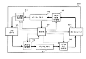
- FIG. 2 is a diagram showing the configuration of the ONU in the PON system according to the first embodiment of the present invention.
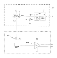
- FIG. 3 is a diagram showing a configuration of an optical transceiver in the ONU according to the first embodiment of the present invention.
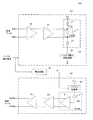
- FIG. 4 is a diagram illustrating a configuration of the bias control unit in the optical transceiver according to the first embodiment of the present invention.
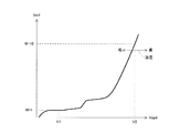
- FIG. 5 is a diagram illustrating an example of the current multiplication characteristic of the light receiving element in the optical transceiver according to the first embodiment of the present invention.
- FIG. 6 is a diagram illustrating an example of the relationship between the reverse bias voltage to the light receiving element and the communication quality in the optical transceiver according to the first embodiment of the present invention.
- FIG. 7 is a diagram illustrating an example of a method for adjusting the reverse bias voltage to the light receiving element in the optical transceiver according to the first embodiment of the present invention.
- FIG. 8 is a diagram schematically showing an example of the arrangement of components in the optical transceiver according to the first embodiment of the present invention.
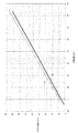
- FIG. 9 is a diagram illustrating a measurement result of a relationship between the temperature of the housing in the optical transceiver according to the first embodiment of the present invention and the detected temperature of the temperature sensor in the CPU.
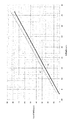
- FIG. 10 is a diagram illustrating a measurement result of a relationship between output values of two temperature sensors in the optical transceiver according to the first embodiment of the present invention.
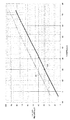
- FIG. 11 is a diagram illustrating a measurement result of the relationship between the environmental temperature and the ROSA temperature in the optical transceiver according to the first embodiment of the present invention.
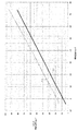
- FIG. 12 is a diagram illustrating a measurement result of the relationship between the environmental temperature and the TOSA temperature in the optical transceiver according to the first embodiment of the present invention.
- FIG. 13 is a diagram illustrating a measurement result of the relationship between the environmental temperature and the surface temperature of the TRX-IC in the optical transceiver according to the first embodiment of the present invention.
- FIG. 14 is a diagram illustrating a measurement result of the relationship between the environmental temperature and the surface temperature of the CPU in the optical transceiver according to the first embodiment of the present invention.
- FIG. 15 is a diagram illustrating a measurement result of a relationship between the environmental temperature and the housing temperature in the optical transceiver according to the first embodiment of the present invention.
- FIG. 16 is a diagram illustrating a measurement result of a temperature transition of each part with respect to a change in environmental temperature in the optical signal transmission-on state according to the first embodiment of the present invention.
- FIG. 17 is a diagram illustrating a measurement result of a temperature transition of each part with respect to a change in environmental temperature in the optical signal transmission off state according to the first embodiment of the present invention.
- FIG. 18 is a diagram illustrating an example of a look-up table used for controlling the reverse bias voltage in the optical transceiver according to the first embodiment of the present invention.
- FIG. 19 is a diagram illustrating an example of a look-up table used for controlling the reverse bias voltage in the optical transceiver according to the first embodiment of the present invention.
- FIG. 20 is a flowchart showing a procedure of a light receiving element control method in the optical transceiver according to the first embodiment of the present invention.
- FIG. 21 is a diagram illustrating a measurement result of temperature transition of each part with respect to transition between the transmission on state and the transmission off state of the optical signal according to the first embodiment of the present invention.
- FIG. 22 is an enlarged view of a part of FIG. FIG.
- FIG. 23 is a diagram illustrating a measurement result of temperature transition of each part with respect to a change between the transmission on state and the transmission off state of the optical signal according to the first embodiment of the present invention.
- FIG. 24 is an enlarged view of a part of FIG.
- FIG. 25 is a diagram illustrating a measurement result of a temperature transition of each part with respect to a change between the transmission on state and the transmission off state of the optical signal according to the first embodiment of the present invention.
- FIG. 26 is an enlarged view of a part of FIG.
- FIG. 27 is a diagram schematically showing an example of the arrangement of components in the ONU according to the second embodiment of the present invention.
- FIG. 28 is a diagram schematically showing an example of the arrangement of components in the optical transceiver according to the second embodiment of the present invention.
- An optical transceiver includes a temperature sensor, an integrated circuit capable of performing arithmetic processing using a temperature detected by the temperature sensor, and an optical module including a light emitting element and a light receiving element.
- the difference between the detected temperature of the temperature sensor in the state and the detected temperature of the temperature sensor in the optical signal transmission off state is greater than 2 ° C., and the power consumption of the transmission driver is the power consumption of the integrated circuit and the optical module Greater than power consumption.
- the optical transceiver has a configuration in which the power consumption, that is, heat generation of the transmission driver is dominant in the thermally conductive casing, and this heat generation causes the temperature rise of the integrated circuit and the optical module. That is, in the optical transceiver, a large amount of power consumption is given to the transmission driver. In other words, a high-intensity optical signal can be output or a high-speed optical signal can be output.
- the optical transceiver has a configuration suitable for use in the optical communication apparatus of (5) below that adjusts the bias voltage by linear calculation using a plurality of target values of the bias voltage. That is, the optical transceiver and the optical communication device of (5) below are suitable for combined use and have the same or corresponding special technical features. Therefore, in the optical transceiver according to the embodiment of the present invention, the bias voltage to the light receiving element can be adjusted well.
- the transmission driver is disposed between the temperature sensor and the optical module.
- the bias voltage to the light receiving element is well adjusted in the optical transceiver in which the temperature sensor is easily affected by the transmission driver and it is difficult to measure the accurate temperature of the optical module by the temperature sensor. Can do.
- the distance between the temperature sensor and the optical module is equal to or less than the distance between the transmission driver and the optical module.
- the influence of the optical module by the transmission driver can be accurately grasped, and the bias voltage to the light receiving element can be determined. It can be adjusted well according to the temperature of the light receiving element.
- An optical transceiver includes a first temperature sensor, a second temperature sensor, an optical module including a light emitting element and a light receiving element, and the second temperature sensor thermally A transmission driver coupled to drive the light emitting element; and a housing that houses the first temperature sensor, the second temperature sensor, the optical module, and the transmission driver, and has thermal conductivity,
- the drive rate of the transmission driver is a, the detected temperature of the first temperature sensor is T1, the detected temperature of the second temperature sensor is T2, the temperature of the light receiving part of the optical module is Tr, and the optical module In the state in which the temperature error allowed for the control of the light receiving unit in Terr is Terr, and the ambient temperature of the housing in the optical signal transmission on state by the light emitting element is a predetermined temperature, a
- the Tr value that can be estimated from T1 and T2 when the value is the minimum value is Tmin
- the Tr value that can be estimated from T1 and T2 when a is the maximum value is Tmax, a is the minimum value
- the optical transceiver a housing having thermal conductivity is provided, and the heat coupling state between the heat generating portion, that is, the transmission driver, and the first temperature sensor and the second temperature sensor is accurately realized.
- the heat coupling state between the heat generating portion, that is, the transmission driver, and the first temperature sensor and the second temperature sensor is accurately realized.
- the error of the temperature Tr of the light receiving unit in the optical module is equal to or less than Terr.
- a bias voltage corresponding to the accurately estimated temperature Tr of the light receiving unit to the light receiving element, it is possible to adjust the multiplication factor according to the temperature of the light receiving element and maintain the optimum value.
- the optical transceiver has a configuration suitable for the use of the optical communication device of (5) below that adjusts the bias voltage by linear calculation using a plurality of target values of the bias voltage. That is, the optical transceiver and the optical communication device of (5) below are suitable for combined use and have the same or corresponding special technical features. Therefore, in the optical transceiver according to the embodiment of the present invention, the bias voltage to the light receiving element can be adjusted well.
- An optical communication apparatus includes a light emitting element, a transmission driver for driving the light emitting element, a light receiving element capable of changing a multiplication factor by a bias voltage, a temperature sensor, and the transmission.
- a calculation unit that calculates a driving rate of the driver, and an adjustment unit that adjusts the bias voltage to the light receiving element, the adjustment unit based on the detection temperature of the temperature sensor and the calculation result of the driving rate,
- the bias voltage is adjusted by a linear operation using a plurality of target values of the bias voltage in a combination of a plurality of temperatures and a plurality of driving rates.
- the optical transceiver operates differently depending on the communication state, specifically, for example, an operation in which the burst duty ratio of the burst optical signal is different, and accordingly, power consumption fluctuates and heat is generated. Even when the amount varies, it is possible to perform control according to the variation of the temperature detected by the temperature sensor. Specifically, for example, by performing feedforward control using a look-up table in accordance with the temperature detected by the temperature sensor and the duty ratio, the bias voltage to the light receiving element is well adjusted according to the temperature of the light receiving element. can do. Therefore, in the optical communication device according to the embodiment of the present invention, it is possible to satisfactorily adjust the bias voltage to the light receiving element.
- a method for controlling a light receiving element includes a light emitting element, a transmission driver for driving the light emitting element, a light receiving element capable of changing a multiplication factor by a bias voltage, and a temperature sensor.
- a method for controlling a light receiving element in an optical communication device comprising: a step of calculating a driving rate of the transmission driver; and a step of adjusting the bias voltage to the light receiving element, wherein the bias voltage is adjusted.
- the bias voltage is adjusted by linear calculation using a plurality of target values of the bias voltage in a combination of a plurality of temperatures and a plurality of the driving rates based on the detection temperature of the temperature sensor and the calculation result of the driving rate. To do.
- the optical transceiver operates differently depending on the communication state, specifically, for example, an operation in which the burst duty ratio of the burst optical signal is different.
- the power consumption fluctuates and the heat generation fluctuates.
- FIG. 1 is a diagram showing a configuration of a PON system according to the first embodiment of the present invention.
- a PON system 301 is, for example, 10G-EPON, and includes ONUs 202A, 202B, and 202C, a station-side device 201 connected to an upper network, and a splitter SP.
- the ONUs 202A, 202B, 202C and the station side device 201 are connected via the splitter SP and the optical fiber OPTF, and transmit / receive optical signals to / from each other.
- FIG. 2 is a diagram showing the configuration of the ONU in the PON system according to the first embodiment of the present invention.
- ONU 202 includes optical transceiver 101, PON reception processing unit 92, buffer memory 93, UN transmission processing unit 94, UNI (User Network Interface) port 95, UN reception processing unit 96, and A buffer memory 97, a PON transmission processing unit 98, and a control unit 99.
- the optical transceiver 101 is detachable from the ONU 202, for example.
- the optical transceiver 101 receives a downstream optical signal transmitted from the station side device 201, converts it into an electrical signal, and outputs it.
- the PON reception processing unit 92 reconstructs a frame from the electrical signal received from the optical transceiver 101, and distributes the frame to the control unit 99 or the UN transmission processing unit 94 according to the type of the frame. Specifically, the PON reception processing unit 92 outputs the data frame to the UN transmission processing unit 94 via the buffer memory 93 and outputs the control frame to the control unit 99.
- the control unit 99 generates a control frame including various control information and outputs it to the UN transmission processing unit 94.
- the UN transmission processing unit 94 transmits the data frame received from the PON reception processing unit 92 and the control frame received from the control unit 99 to a user terminal such as a personal computer (not shown) via the UNI port 95.
- the UN reception processing unit 96 outputs the data frame received from the user terminal via the UNI port 95 to the PON transmission processing unit 98 via the buffer memory 97, and the control frame 99 receives the control frame received from the user terminal via the UNI port 95. Output to.
- the control unit 99 performs home-side processing related to control and management of the PON line between the station-side device 201 and the ONU 202, such as MPCP and OAM. That is, various controls such as access control are performed by exchanging MPCP messages and OAM messages with the station-side apparatus 201 connected to the PON line.
- the control unit 99 generates a control frame including various control information and outputs it to the PON transmission processing unit 98.
- the control unit 99 performs various setting processes for each unit in the ONU 202.
- the PON transmission processing unit 98 outputs the data frame received from the UN reception processing unit 96 and the control frame received from the control unit 99 to the optical transceiver 101.
- the optical transceiver 101 converts the data frame and control frame, which are electrical signals received from the PON transmission processing unit 98, into optical signals and transmits them to the station-side apparatus 201.
- FIG. 3 is a diagram showing a configuration of an optical transceiver in the ONU according to the first embodiment of the present invention.
- the optical transceiver 101 includes a burst transmission unit 151, a reception unit 152, and an integration circuit (calculation unit) 84.
- the burst transmission unit 151 includes a preamplifier 86, an output buffer circuit (modulation current supply circuit) 87, a bias current supply circuit 88, and a light emitting circuit 89.
- the light emitting circuit 89 includes a light emitting element LD and inductors L1 and L2.
- the receiving unit 152 includes a light receiving element PD, a TIA (transimpedance amplifier) 81, an LIA (limit amplifier) 82, a bias control unit (adjusting unit) 83, and an output buffer 85.
- the preamplifier 86 receives the data frame from the UN reception processing unit 96 and the transmission data that is the control frame from the control unit 99, and amplifies and outputs the transmission data.
- the preamplifier 86 receives the transmission data as a differential signal from the signal lines INP and INN.
- the output buffer circuit 87 supplies a modulation current to the light emitting circuit 89 based on the transmission data received from the preamplifier 86.
- This modulation current is a current having a magnitude corresponding to the logical value of data to be transmitted to the station side device 201.
- the light emitting circuit 89 transmits an upstream optical signal to the station side device 201.
- the light emitting element LD is connected to a power supply node supplied with a fixed voltage, for example, a power supply voltage Vcc, via an inductor L1, and is connected to a bias current supply circuit 88 via an inductor L2.
- the light emitting element LD emits light based on the bias current supplied from the bias current supply circuit 88 and the modulation current supplied from the output buffer circuit 87, and changes the light emission intensity.
- the burst transmission unit 151 whether to supply power to the preamplifier 86 and the output buffer circuit 87 is switched based on the burst control signal received from the control unit 99. Specifically, power is supplied to the preamplifier 86 and the output buffer circuit 87 when the burst control signal is activated, and the power supply is stopped when the burst control signal is deactivated.
- the bias current supply circuit 88 starts supplying a bias current when a burst control signal for transmitting a burst optical signal is activated. That is, the bias current supply circuit 88 switches whether to supply a bias current to the light emitting circuit 89 based on the burst control signal received from the control unit 99.
- the value of the bias current is set such that the light emitting element LD emits light when the bias current is supplied to the light emitting element LD in the state where the modulation current to the light emitting element LD is zero. Is set.
- the integrating circuit 84 calculates the burst duty ratio of the burst optical signal. Specifically, integration circuit 84 integrates, for example, the burst control signal received from control unit 99 and outputs voltage Vi having a level corresponding to the integration value to bias control unit 83.
- the light receiving element PD is, for example, an avalanche photodiode.
- the light receiving element PD converts the optical signal received from the station side device 201 into an electric signal, for example, an electric current and outputs it.
- the TIA 81 converts the current received from the light receiving element PD into a voltage and outputs it to the LIA 82.
- the LIA 82 binarizes the voltage level received from the TIA 81 and outputs it as received data.
- the output buffer 85 amplifies the reception data received from the LIA 82 and outputs the amplified data to the PON reception processing unit 92.
- the output buffer 85 outputs the received data from the signal lines OUTP and OUTN as a differential signal.
- the bias control unit 83 includes a processor that performs logical operation processing, such as a CPU (Central Processing Unit), an MPU (Micro-Processing Unit), or an FPGA (Field-Programmable Gate Array).
- Bias control unit 83 is connected to a power supply node supplied with a fixed voltage, for example, power supply voltage Vcc, and supplies a bias voltage to light receiving element PD.
- the bias controller 83 has a bias voltage adjustment function.
- the light emitting element LD is built in an assembled light emitting module (hereinafter also referred to as TOSA: Transmitter Optical Sub-Assembly).
- the light receiving element PD and the TIA 81 are built in an assembled light receiving module (hereinafter also referred to as ROSA: Receiver Optical Sub-Assembly).
- FIG. 4 is a diagram showing a configuration of a bias control unit in the optical transceiver according to the first embodiment of the present invention.
- the bias control unit 83 includes a CPU 11, a resistor 14, and a DC / DC converter 15.
- the CPU 11 includes a temperature sensor 21 and a storage unit 23.
- the resistance value of the resistor 14 is Ra.
- the light receiving element PD has a cathode connected to the DC / DC converter 15 and an anode connected to the input end of the TIA 81.
- Resistor 14 has a first end connected to the output end of CPU 11 and the input end of DC / DC converter 15, and a second end connected to the ground node.
- a power supply voltage Vcc is supplied to the DC / DC converter 15 and the TIA 81.
- the light receiving element PD outputs a current Iapd corresponding to the intensity of the optical signal Pin1 received from the station side device 201 via the optical fiber OPTF to the TIA 81.
- the light receiving element PD can change the multiplication factor M by the reverse bias voltage Vapd.
- the CPU 11 adjusts the reverse bias voltage Vapd to the light receiving element PD. As will be described later, the CPU 11 can perform arithmetic processing using the temperature detected by the temperature sensor 21.
- the DC / DC converter 15 supplies the reverse bias voltage Vapd to the light receiving element PD in accordance with the adjustment of the reverse bias voltage Vapd by the CPU 11.
- the CPU 11 generates and outputs a current Ictrl.
- the current Ictrl is converted into a voltage Vctrl by the resistor 14 and supplied to the DC / DC converter 15.
- the DC / DC converter 15 supplies the reverse bias voltage Vapd to the light receiving element PD based on the voltage Vctrl received from the CPU 11.
- the CPU 11 converts the control digital value into the current Ictrl by using a built-in D / A converter.
- the number of components in the optical transceiver 101 can be reduced by using the built-in components of the CPU 11.
- the relationship between the control digital value applied to the D / A converter and the reverse bias voltage Vapd is a linear relationship.
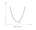
- FIG. 5 is a diagram showing an example of the current multiplication characteristic of the light receiving element in the optical transceiver according to the first embodiment of the present invention.
- the horizontal axis represents the reverse bias voltage Vapd
- the vertical axis represents the output current Iapd.
- the output current Iapd increases as the reverse bias voltage Vapd to the light receiving element PD increases. That is, the multiplication factor M increases.
- the multiplication factor M of the light receiving element PD is constant without causing avalanche multiplication even if the reverse bias voltage Vapd is changed within a certain range.
- the multiplication factor M at this time is 1.
- the output current Iapd becomes 10 times that when the reverse bias voltage Vapd is V1. That is, when the reverse bias voltage Vapd is V2, the multiplication factor M is 10.
- the multiplication factor M of the light receiving element PD has a strong temperature characteristic. As shown in FIG. 5, the output current Iapd decreases as the temperature of the light receiving element PD increases, and the output current Iapd decreases as the temperature of the light receiving element PD decreases. Becomes larger. That is, when the temperature of the light receiving element PD increases, the multiplication factor M with respect to the reverse bias voltage Vapd decreases, and when the temperature of the light receiving element PD decreases, the multiplication factor M with respect to the reverse bias voltage Vapd increases.
- FIG. 6 is a diagram showing an example of the relationship between the reverse bias voltage to the light receiving element and the communication quality in the optical transceiver according to the first embodiment of the present invention.
- the horizontal axis represents the reverse bias voltage Vapd
- the vertical axis represents the bit error rate.
- the reverse bias voltage Vapd when the reverse bias voltage Vapd is set so that the multiplication factor M is 10 and the multiplication factor M is reduced by decreasing the reverse bias voltage Vapd, the light receiving sensitivity of the light receiving element PD is reduced and the intensity is lower. Since it becomes difficult to receive an optical signal, the S / N (Signal to Noise Ratio) ratio deteriorates and the bit error rate increases.
- the multiplication factor M there is an optimum value for the multiplication factor M, for example, around 10 is the optimum value. Further, as described with reference to FIG. 5, the multiplication factor M has temperature characteristics. Therefore, it is necessary to adjust the multiplication factor M according to the temperature of the light receiving element PD and maintain the optimum value.
- the CPU 11 in the bias control unit 83 adjusts the output current Ictrl so that the multiplication factor M becomes a target value.
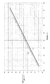
- FIG. 7 is a diagram showing an example of a method for adjusting the reverse bias voltage to the light receiving element in the optical transceiver according to the first embodiment of the present invention.
- the horizontal axis represents the detected temperature of the temperature sensor 21, and the vertical axis represents the reverse bias voltage Vapd.
- the reverse bias voltage Vapd at which the multiplication factor M becomes the optimum value is actually measured at three temperatures of low temperature, normal temperature, and high temperature, specifically, 0 ° C., 28 ° C., and 74 ° C.
- the measurement is performed in an optical signal transmission on state by the light emitting element LD, specifically in a state in which the burst control signal is activated and the light emitting element LD emits light based on the bias current and the modulation current.
- the optical transceiver 101 may have a configuration in which the light emitting element LD does not emit light in a state where a bias current is supplied to the light emitting element LD.
- the transmission on state and the transmission off state of the optical signal correspond to the on state and the off state of the light emitting element LD, respectively.
- a look-up table showing the correspondence between the detected temperature of the temperature sensor 21 and the control digital value of the D / A converter built in the CPU 11 in, for example, a 2 ° C. step is created, and the storage unit 23 in the optical transceiver 101 is created. Save to.
- the CPU 11 acquires a control digital value corresponding to the temperature detected by the temperature sensor 21 from the look-up table and gives it to the D / A converter.
- FIG. 8 is a diagram schematically showing an example of the arrangement of the components in the optical transceiver according to the first embodiment of the present invention.
- the optical transceiver 101 includes a housing K, a sub board B1, and a BOSA (Bidirectional Optical Sub-Assemblies) optical module 13.
- BOSA Bidirectional Optical Sub-Assemblies
- each unit shown in FIG. 2 is mounted on a parent board (not shown). Further, the sub board B1 is connected to the parent board via the connector 16.
- a CPU 11 that is an integrated circuit On the slave board B1, a CPU 11 that is an integrated circuit, a TRX-IC (Integrated Circuit) 12 that is an integrated circuit, and a connector 16 are mounted.
- TRX-IC Integrated Circuit
- FIG. 8 representatively shows a main signal line (TX) on the transmission side and a main signal line (RX) on the reception side.
- the TRX-IC 12 includes, for example, a preamplifier 86, an output buffer circuit 87, a bias current supply circuit 88, an LIA 82, and an output buffer 85.
- the TRX-IC 12 includes a temperature sensor 22, for example.
- the BOSA optical module 13 is an optical module in which a TOSA that is a light emitting unit and a ROSA that is a light receiving unit are integrated.
- the TOSA portion in the BOSA optical module 13 is also simply referred to as TOSA
- the ROSA portion in the BOSA optical module 13 is also simply referred to as ROSA.
- the housing K is mounted on the parent board and accommodates the child board B1 and the BOSA optical module 13.
- the casing K has an elongated shape.
- the TRX-IC 12 is disposed between the temperature sensor 21 and the BOSA optical module 13. More specifically, the connector 16, the CPU 11, the TRX-IC 12, and the BOSA optical module 13 are arranged in this order in the housing K, and the arrangement direction is along the longitudinal direction of the housing K. Further, for example, the distance between the CPU 11 and the TRX-IC 12 is smaller than the distance between the BOSA optical module 13 and the TRX-IC 12.
- the housing K has thermal conductivity and is made of, for example, metal. That is, each member is covered with the heat conducting member so that the ambient temperature of the housing K affects the members accommodated in the housing K evenly.
- the power consumption of the TRX-IC 12 is larger than the power consumption of the CPU 11 and the BOSA optical module 13. More specifically, in the circuit on the transmission side accommodated in the housing K, the power consumption of the transmission driver DV that drives the light emitting element LD in the TRX-IC 12 is the largest.
- the internal temperature of the housing K changes greatly in the transmission-on state and the transmission-off state of the optical signal.
- the change in the temperature detected by the temperature sensor 21 in the CPU 11 is more than the change in the ambient temperature of the light receiving element PD in the BOSA optical module 13. Also grows.
- the transmission driver DV corresponds to at least one of the preamplifier 86, the output buffer circuit 87, and the bias current supply circuit 88.
- the temperature sensor 22 is thermally coupled to the transmission driver DV.
- the optical signal transmission off state that is, the burst control signal is inactive.
- the power consumption of the transmission driver DV is reduced, and the internal temperature of the housing K is also reduced, so that the temperature relationship assumed in the lookup table is broken. That is, it becomes difficult to satisfactorily adjust the reverse bias voltage Vapd according to the temperature.
- the relationship of the lookup table is broken depending on the duty ratio of the burst, that is, the burst-on ratio.
- the TOSA is provided with a heat dissipation sheet
- the ROSA, the CPU 11 and the TRX-IC 12 use the optical transceiver 101 without the heat dissipation sheet.
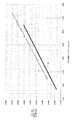
- FIG. 9 is a diagram showing a measurement result of the relationship between the temperature of the casing in the optical transceiver according to the first embodiment of the present invention and the detected temperature of the temperature sensor in the CPU.
- the horizontal axis represents the temperature of the housing
- the vertical axis represents the temperature detected by the temperature sensor 21 in the CPU 11.
- Graph G1 shows a transmission on state
- graph G2 shows a transmission off state.
- casing K is the temperature of the position of TOSA vicinity.
- the temperature sensor 21 is used to indicate the temperature of the housing K. More specifically, the detected value of the temperature sensor 21 is calculated by substituting a digital value obtained by converting the output signal of the temperature sensor 21 by the A / D converter into a predetermined conversion formula. The coefficient in this conversion equation is calculated using digital values of the A / D converter at low temperatures and high temperatures in the optical signal transmission on state.
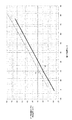
- FIG. 10 is a diagram showing a measurement result of the relationship between the output values of the two temperature sensors in the optical transceiver according to the first embodiment of the present invention.
- the horizontal axis represents the output digital value of the temperature sensor 21 in the CPU 11
- the vertical axis represents the output digital value of the temperature sensor 22 in the TRX-IC 12.
- Graph G3 shows the transmission on state
- graph G4 shows the transmission off state.
- FIG. 11 is a diagram showing a measurement result of the relationship between the environmental temperature and the ROSA temperature in the optical transceiver according to the first embodiment of the present invention.
- the horizontal axis represents the environmental temperature
- the vertical axis represents the ROSA temperature.
- Graph G5 shows a transmission on state
- graph G6 shows a transmission off state.
- FIG. 12 is a diagram showing a measurement result of the relationship between the environmental temperature and the temperature of the TOSA in the optical transceiver according to the first embodiment of the present invention.
- the horizontal axis represents the environmental temperature
- the vertical axis represents the TOSA temperature.
- Graph G7 shows a transmission on state
- graph G8 shows a transmission off state.
- FIG. 13 is a diagram showing measurement results of the relationship between the environmental temperature and the surface temperature of the TRX-IC in the optical transceiver according to the first embodiment of the present invention.
- the horizontal axis is the ambient temperature
- the vertical axis is the surface temperature of the TRX-IC 12.
- a graph G9 shows a transmission on state
- a graph G10 shows a transmission off state.
- FIG. 14 is a diagram showing a measurement result of the relationship between the environmental temperature and the surface temperature of the CPU in the optical transceiver according to the first embodiment of the present invention.
- the horizontal axis is the environmental temperature
- the vertical axis is the surface temperature of the CPU 11.
- Graph G11 shows a transmission on state
- graph G12 shows a transmission off state.
- FIG. 15 is a diagram showing a measurement result of the relationship between the environmental temperature and the casing temperature in the optical transceiver according to the first embodiment of the present invention.
- the horizontal axis represents the environmental temperature
- the vertical axis represents the temperature of the housing.
- Graph G13 shows a transmission on state
- graph G14 shows a transmission off state.
- casing K is the temperature of the position of TOSA vicinity.
- the surface of TRX-IC 12 has the largest temperature deviation between the transmission on state and the transmission off state. This indicates that the power consumption of the TRX-IC 12 is larger than that of other circuits.
- the temperature deviation between the transmission on state and the transmission off state is small in the ROSA, but is large on the surface of the CPU 11. Since the CPU 11 originally does not greatly change the processing amount between the transmission on state and the transmission off state, the difference in power consumption should be small, and the power consumption is smaller than that of the TRX-IC 12.
- the temperature deviation between the transmission on state and the transmission off state is small in the TOSA, but is large on the surfaces of the CPU 11 and the TRX-IC 12.
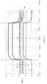
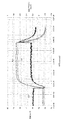
- FIG. 16 is a diagram illustrating a measurement result of a temperature transition of each part with respect to a change in environmental temperature in the optical signal transmission-on state according to the first embodiment of the present invention.
- the horizontal axis is time, and the vertical axis is temperature.
- Graph G81 shows the temperature of TRX-IC12
- Graph G82 shows the surface temperature of CPU 11
- Graph G83 shows the temperature of ROSA
- Graph G84 shows the temperature of TOSA
- Graph G85 shows the case K.
- the graph G86 shows the temperature detected by the temperature sensor 21.
- FIG. 17 is a diagram showing a measurement result of temperature transition of each part with respect to a change in environmental temperature in the optical signal transmission off state according to the first embodiment of the present invention.
- the horizontal axis is time, and the vertical axis is temperature.
- Graph G91 shows the temperature of TRX-IC 12
- graph G92 shows the surface temperature of CPU 11
- graph G93 shows the temperature of ROSA
- graph G94 shows the temperature of TOSA
- graph G95 shows the case K.
- the graph G96 shows the temperature detected by the temperature sensor 21.
- the temperature of the casing K changes due to the change of the environmental temperature, and the temperature of each part in the casing K is the temperature of the casing K. It can be seen that it has changed in a similar manner.
- the present inventors have devised an optimal control method for the reverse bias voltage Vapd in the optical transceiver 101 as follows.
- the reverse bias voltage Vapd is controlled by the method shown in (1) to (4).
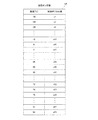
- FIG. 18 is a diagram showing an example of a look-up table used for controlling the reverse bias voltage in the optical transceiver according to the first embodiment of the present invention.
- look-up table ta1 is created in (1) above, and for example, linear approximation is performed using measurement results obtained when temperature sensor 21 detects temperatures of 0 ° C., 28 ° C., and 74 ° C. The results are shown.
- control digital values x1 to x63 are registered in steps of 2 ° C over a range of -30 ° C to 94 ° C by interpolating between measured temperatures with a straight line.
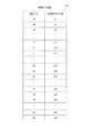
- FIG. 19 is a diagram showing an example of a look-up table used for controlling the reverse bias voltage in the optical transceiver according to the first embodiment of the present invention.
- look-up table ta2 is created in the above (2), and for example, linear approximation is performed using the measurement results obtained when temperature sensor 21 detects temperatures of 0 ° C., 28 ° C., and 74 ° C. The results are shown.
- control digital values y1 to y63 are registered in steps of 2 ° C. over ⁇ 30 ° C. to 94 ° C. by linearly interpolating between measured temperatures.
- control digital value y31 + (x31 ⁇ y31) ⁇ 0.1
- control digital value y15 + (x15 ⁇ y15) ⁇ 0.8
- the optical transceiver 101 when the difference between the detected temperature of the temperature sensor 21 in the transmission on state and the detected temperature of the temperature sensor 21 in the transmission off state is larger than 2 ° C., that is, larger than the control step width of the look-up tables ta1 and ta2.
- the method for controlling the reverse bias voltage Vapd as described above is useful. Further, for example, from the measurement result shown in FIG. 9, when the difference between the detected temperatures of the temperature sensor 21 in the transmission on state and the transmission off state is 8 ° C. or more, the control method of the reverse bias voltage Vapd as described above becomes more useful. preferable.
- bias control unit 83 has reverse bias voltage Vapd at a combination of a plurality of temperatures and a plurality of duty ratios based on the temperature detected by temperature sensor 21 and the calculation result of the duty ratio by integration circuit 84.
- the reverse bias voltage Vapd is adjusted by linear calculation using a plurality of target values.
- the storage unit 23 in the CPU 11 stores a correspondence relationship between the target value of the reverse bias voltage Vapd and the temperature for each duty ratio.
- the bias controller 83 adjusts the reverse bias voltage Vapd based on a plurality of target values corresponding to the detected temperatures of the temperature sensor 21 and the calculation result of the duty ratio in the correspondence relationship.
- the storage unit 23 stores the lookup tables ta1 and ta2 as described above.
- the CPU 11 refers to the look-up tables ta1 and ta2, acquires a control digital value based on the voltage Vi received from the integration circuit 84 and the temperature detected by the temperature sensor 21, and has a magnitude corresponding to the acquired control digital value.
- a current Ictrl is generated and output.
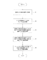
- FIG. 20 is a flowchart showing a procedure of a method for controlling a light receiving element in the optical transceiver according to the first embodiment of the present invention.
- the duty ratio a of the burst of the optical signal is calculated.
- the reverse bias voltage Vapd to the light receiving element PD is adjusted.
- reverse bias is performed by linear calculation using a plurality of target values of the reverse bias voltage Vapd at a combination of a plurality of temperatures and a plurality of duty ratios a. The voltage Vapd is adjusted.
- the CPU 11 acquires the detected temperature T1 of the temperature sensor 21 (step S1).
- the CPU 11 acquires the burst duty ratio a of the burst optical signal based on the voltage Vi received from the integration circuit 84 (step S2).
- the CPU 11 reads the lookup table ta1 in the storage unit 23, and obtains the control digital value A corresponding to the target value of the reverse bias voltage Vapd at the detection temperature T1 in the transmission ON state from the lookup table ta1 (step S3). ).
- the CPU 11 reads the lookup table ta2 in the storage unit 23, and obtains the control digital value B corresponding to the target value of the reverse bias voltage Vapd at the detection temperature T1 in the transmission off state from the lookup table ta2 (step S4). ).
- the CPU 11 adjusts the reverse bias voltage Vapd by a linear calculation using the duty ratio a, the control digital value A, and the control digital value B. Specifically, the CPU 11 calculates a control digital value of the built-in D / A converter, for example, according to the following equation (step S5).
- Control digital value B + (A ⁇ B) ⁇ a
- steps S1 and S2 may be switched. Further, the order of some or all of steps S2 to S4 may be changed.
- the environmental temperature is Ta
- the temperature of the ROSA in the transmission-on state is Tr
- the temperature of the CPU 11 is Tc
- the temperature of the TRX-IC 12 is Tl.
- Tr 1.0157 ⁇ Ta + 9.5013
- Tl 0.9906 ⁇ Ta + 22.413
- Tc 1.0289 ⁇ Ta + 17.701
- the temperature of the ROSA is set to Trd
- the temperature of the CPU 11 is set to Tcd
- the temperature of the TRX-IC 12 is set to Tld.
- Trd 0.9911 ⁇ Ta + 6.627
- Tld 1.0027 ⁇ Ta + 8.33841
- Tcd 0.9877 ⁇ Ta + 8.1261
- Tr ⁇ Trd ⁇ 9.66041 ⁇ Tc + 10.00029 ⁇ Tl + 51.25998 (6)
- Tr_a Trd + a ⁇ (Tr ⁇ Trd) (7)
- Tr_a (12.0204-9.6041 * a) * Tc + (-11.469469 + 10.00029 * a) * Tl + (1-a) * 51.25998
- the ROSA temperature Tr_a corresponding to the temperature of the light receiving element PD to which the reverse bias voltage Vapd is applied can be expressed by an approximate model expression using a, Tc, and Tl.
- the surface temperature of the CPU 11 is used as Tc
- the surface temperature of the TRX-IC 12 is used as Tl. These are used to control the actual reverse bias voltage Vapd. These correspond to the detected temperatures of the temperature sensors 21 and 22 used.
- the present inventor further examined the feasibility of the above approximate model including temperature transition.
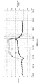
- FIG. 21 is a diagram showing the measurement results of the temperature transition of each part with respect to the transition between the transmission on state and the transmission off state of the optical signal according to the first embodiment of the present invention.
- the horizontal axis is time and the vertical axis is temperature.
- Graph G21 shows the temperature of TRX-IC12
- Graph G22 shows the surface temperature of CPU 11
- Graph G23 shows the temperature of ROSA
- Graph G24 shows the calculated value by the approximate expression of the temperature of ROSA
- Graph G25 indicates the temperature of the TOSA
- the graph G26 indicates the temperature of the housing K
- the graph G27 indicates the environmental temperature
- the graph G28 indicates the detected temperature of the temperature sensor 21.
- FIG. 21 shows the measurement results in an environment of ⁇ 5 ° C.
- the temperature of each part increases from around time t1 when switching from the transmission off state to the transmission on state, and converges in about 6 minutes.
- part falls from the time t2 vicinity which is switched from a transmission ON state to a transmission OFF state, and has converged in about 6 minutes.
- FIG. 22 is an enlarged view of a part of FIG. In FIG. 22, the horizontal axis is time, and the vertical axis is temperature.
- the graph G31 shows the temperature of the ROSA
- the graph G32 shows the calculated value by the approximate expression of the temperature of the ROSA
- the graph G33 shows the temperature penalty showing the estimation error, that is, the difference between the graphs G31 and G32.
- the difference between the measured value and the calculated value of the ROSA temperature is approximately 0 ° C. to + 0.4 ° C.
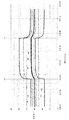
- FIG. 23 is a diagram showing a measurement result of a temperature transition of each part with respect to a change between the transmission on state and the transmission off state of the optical signal according to the first embodiment of the present invention.
- the horizontal axis is time, and the vertical axis is temperature.
- Graph G41 shows the temperature of TRX-IC12
- Graph G42 shows the surface temperature of CPU 11
- Graph G43 shows the temperature of ROSA
- Graph G44 shows the calculated value by the approximate expression of the temperature of ROSA
- Graph G45 indicates the temperature of the TOSA
- the graph G46 indicates the temperature of the housing K
- the graph G47 indicates the environmental temperature
- the graph G48 indicates the detected temperature of the temperature sensor 21.
- FIG. 23 shows the measurement results in an environment of + 25 ° C.
- the temperature of each part increases from around time t11 when switching from the transmission off state to the transmission on state, and converges in about 6 minutes. And the temperature of each part falls from the time t12 vicinity which is switched from the transmission ON state to the transmission OFF state, and converges in about 6 minutes.
- FIG. 24 is an enlarged view of a part of FIG.
- the horizontal axis is time
- the vertical axis is temperature.
- the graph G51 shows the temperature of the ROSA
- the graph G52 shows the calculated value by the approximate expression of the temperature of the ROSA
- the graph G53 shows the temperature penalty showing the estimation error, that is, the difference between the graphs G51 and G52.
- the difference between the measured value and the calculated value of the ROSA temperature is approximately ⁇ 0.6 ° C. to + 0 ° C.
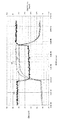
- FIG. 25 is a diagram showing a measurement result of a temperature transition of each part with respect to a change between the transmission on state and the transmission off state of the optical signal according to the first embodiment of the present invention.
- the horizontal axis is time, and the vertical axis is temperature.
- Graph G61 shows the temperature of TRX-IC12
- Graph G62 shows the surface temperature of CPU 11
- Graph G63 shows the temperature of ROSA
- Graph G64 shows the calculated value by the approximate expression of the temperature of ROSA
- Graph G65 indicates the temperature of the TOSA
- the graph G66 indicates the temperature of the housing K
- the graph G67 indicates the environmental temperature
- the graph G68 indicates the detected temperature of the temperature sensor 21.
- FIG. 25 shows the measurement results in an environment of + 70 ° C.
- the temperature of each part increases from around time t31 when switching from the transmission off state to the transmission on state, and converges in about 6 minutes. Then, the temperature of each part decreases from around time t32 when the transmission on state is switched to the transmission off state, and converges in about 6 minutes.
- FIG. 26 is an enlarged view of a part of FIG.
- the horizontal axis is time
- the vertical axis is temperature.
- the graph G71 shows the temperature of the ROSA
- the graph G72 shows the calculated value by the approximate expression of the temperature of the ROSA
- the graph G73 shows the temperature penalty showing the estimation error, that is, the difference between the graphs G71 and G72.
- the difference between the actually measured value and the calculated value of the ROSA temperature is approximately ⁇ 0.2 ° C. to + 0.6 ° C.
- Tr_a (2.132436 + 0.618751 ⁇ a) ⁇ Tc ⁇ (1.1555 + 0.6018 ⁇ a) ⁇ Tl + (a ⁇ 1) ⁇ 6.793542
- the temperature penalty is not 0.7 ° C. in both positive and negative directions, and during temperature transient In particular, slight fluctuations are observed at high temperatures.
- the inventor of the present application can estimate the temperature Tr_a of the ROSA by using an approximate model expression using a, Tc, and Tl including the middle of the temperature transition. We obtained the knowledge that the term containing is unnecessary.
- the duty ratio of the burst of the optical signal is a
- the detection temperature of the temperature sensor 21 is T1
- the detection temperature of the temperature sensor 22 is T2
- the temperature of the light receiving unit of the BOSA optical module 13 is Tr.
- the temperature error allowed for the control of the light receiving unit in the BOSA optical module 13 is Terr.
- the value of Tr that can be estimated from T1 and T2 when a is the minimum value is Tmin
- the value of Tr that can be estimated from T2 is Tmax.
- the measured value of Tr is calculated with respect to the estimated value of Tr obtained by dividing Tmin and Tmax by a.
- the error is equal to or less than Terr.
- the temperature error Terr is 2 ° C. which is the step width of the look-up tables ta1 and ta2. From FIG. 21 to FIG. 26, in the optical transceiver 101, the error of the temperature Tr of ROSA, that is, the absolute value of the temperature penalty is less than 0.7 ° C.
- the optical transceiver 101 applies the reverse bias voltage Vapd corresponding to the estimated ROSA temperature Tr_a to the light receiving element PD, thereby adjusting the multiplication factor M according to the temperature of the light receiving element PD, and setting the optimum value. Can be maintained.
- the optical transceiver 101 is provided with a case K having thermal conductivity, and the heat coupling state between the heat generation portion, that is, the transmission driver DV, and the temperature sensors 21 and 22 is accurately realized, so that the temperature of the ROSA is increased.
- a good thermal coupling state in which the Tr error is equal to or less than Terr can be realized.
- the CPU 11 is configured to adjust the reverse bias voltage Vapd based on the temperature detected by the temperature sensor 21, but the present invention is not limited to this. .
- the CPU 11 may be configured to adjust the reverse bias voltage Vapd based on the temperature detected by the temperature sensor 22 in the TRX-IC 12.
- the look-up tables ta1 and ta2 may be created using the detected temperature of the temperature sensor 22.
- the temperature sensor 21 is configured to be built in the CPU 11, but the present invention is not limited to this.
- the temperature sensor 21 may be provided outside the CPU 11.
- the temperature sensor 22 is built in the TRX-IC 12.
- the present invention is not limited to this.
- the temperature sensor 22 only needs to be thermally coupled to the TRX-IC 12 and may be configured to be provided outside the TRX-IC 12.
- the burst duty ratio of the burst optical signal is used in the control of the reverse bias voltage Vapd.
- the present invention is not limited to this. Not only the duty ratio but also other types of values may be used as long as they indicate the driving rate of the transmission driver DV.
- optical transceiver is configured to include the bias control unit 83 and the integration circuit 84
- the present invention is not limited to this.
- the bias control unit 83 and the integration circuit 84 may be configured to be provided outside the optical transceiver 101 in the ONU 202.
- optical transceiver according to the first embodiment of the present invention is configured to include the temperature sensor 22, the configuration is not limited thereto, and a configuration not including the temperature sensor 22 may be used.
- the ONU including the optical transceiver is exemplified, but the present invention is widely applicable to optical communication apparatuses. Further, the present invention is suitable for use in an optical communication device that transmits burst optical signals. In particular, it is more effective when used in a home-side device in a PON system, in which many are manufactured according to the same specifications at the time of manufacture, and in actual use, the multiplication factor of the light receiving element will be different depending on the environment of the installation location. It is.
- feedforward control is performed using a temperature sensor and a look-up table related to the temperature in the optical transceiver.
- the detected temperature of the temperature sensor also fluctuates.
- the transmission driver DV drives the light emitting element LD.
- the light receiving element PD can change the multiplication factor by the reverse bias voltage Vapd.
- the integration circuit 84 calculates the drive rate a of the transmission driver DV, for example, the duty ratio a of the burst of the burst optical signal.
- the bias controller 83 adjusts the reverse bias voltage Vapd to the light receiving element PD.
- the bias control unit 83 performs linear calculation using a plurality of target values of the reverse bias voltage Vapd at a combination of a plurality of temperatures and a plurality of driving rates a based on the detection temperature of the temperature sensor 21 and the calculation result of the driving rate a. To adjust the reverse bias voltage Vapd.
- the optical communication device performs different operations depending on the communication state, specifically, for example, an operation in which the burst duty ratio of the burst optical signal is different, and the power consumption fluctuates accordingly. Even when the amount of heat generation varies, control according to the variation in the temperature detected by the temperature sensor can be performed. Specifically, for example, by performing feedforward control using the look-up tables ta1 and ta2 according to the detected temperature of the temperature sensor 21 and the duty ratio a, the reverse bias voltage Vapd to the light receiving element PD is changed to the light receiving element. It can adjust favorably according to the temperature of PD.
- the bias voltage to the light receiving element can be adjusted well.
- the CPU 11 can perform arithmetic processing using the temperature detected by the temperature sensor 21.
- the BOSA optical module 13 includes a light emitting element LD and a light receiving element PD.
- the transmission driver DV drives the light emitting element LD.
- the housing K accommodates the temperature sensor 21, the CPU 11, the BOSA optical module 13, and the transmission driver DV, and has thermal conductivity. The difference between the temperature detected by the temperature sensor 21 in the transmission on state and the temperature detected by the temperature sensor 21 in the transmission off state is greater than 2 ° C.
- the power consumption of the transmission driver DV is larger than the power consumption of the CPU 11 and the power consumption of the BOSA optical module 13.
- the power consumption that is, heat generation of the transmission driver DV is dominant in the casing K having thermal conductivity, and this heat generation increases the temperature of the integrated circuit, that is, the CPU 11 and the BOSA optical module 13. It is the composition that causes. That is, in the optical transceiver 101, a large amount of power consumption is applied to the transmission driver DV. In other words, a high-intensity optical signal may be output or a high-speed optical signal may be output. it can.
- the optical transceiver 101 has a configuration suitable for use of an optical communication device that adjusts the reverse bias voltage Vapd by linear calculation using a plurality of target values of the reverse bias voltage Vapd described above. That is, the optical transceiver 101 and the optical communication device are suitable for combined use and have the same or corresponding special technical features.
- the bias voltage to the light receiving element can be adjusted well.
- the transmission driver DV is disposed between the temperature sensor 21 and the BOSA optical module 13.
- the bias to the light receiving element PD is set.
- the voltage can be adjusted well.
- the BOSA optical module 13 includes a light emitting element LD and a light receiving element PD.
- the temperature sensor 22 is thermally coupled to drive the light emitting element LD.
- the housing K houses the temperature sensor 21, the temperature sensor 22, the BOSA optical module 13, and the transmission driver DV, and has thermal conductivity.
- the driving rate of the transmission driver DV is a, the detected temperature of the temperature sensor 21 is T1, the detected temperature of the temperature sensor 22 is T2, the temperature of the light receiving unit of the BOSA optical module 13 is Tr, and the light receiving unit in the BOSA optical module 13 Let Terr be the temperature error allowed for the control.
- the value of Tr that can be estimated from T1 and T2 when a is the minimum value is Tmin
- the value of Tr that can be estimated from T2 is Tmax.
- the measured value of Tr is calculated with respect to the estimated value of Tr obtained by dividing Tmin and Tmax by a.
- the error is equal to or less than Terr.
- the optical transceiver 101 includes the housing K having thermal conductivity, and the heat coupling state between the heat generation portion, that is, the transmission driver DV, and the temperature sensors 21 and 22 is accurately realized, so that BOSA It is possible to realize a good thermal coupling state in which the error of the ROSA temperature Tr in the optical module 13 is Terr or less.
- the multiplication factor M can be adjusted according to the temperature of the light receiving element PD, and the optimum value can be maintained. .
- the optical transceiver 101 has a configuration suitable for use of an optical communication device that adjusts the reverse bias voltage Vapd by linear calculation using a plurality of target values of the reverse bias voltage Vapd described above.
- the optical communication device and the optical transceiver 101 are suitable for combined use and have the same or corresponding special technical features.
- the bias voltage to the light receiving element can be adjusted well.
- the drive rate a of the transmission driver DV is calculated.
- the reverse bias voltage Vapd to the light receiving element PD is adjusted.
- a plurality of target values of the reverse bias voltage Vapd at a combination of a plurality of temperatures and a plurality of drive rates a are used based on the detection temperature of the temperature sensor 21 and the calculation result of the drive rate a.
- the reverse bias voltage Vapd is adjusted by the linear calculation.
- the optical transceiver 101 performs different operations depending on the communication state, specifically, for example, an operation in which the burst duty ratio of the burst optical signal is different. Even if it fluctuates, it is possible to perform control according to fluctuations in the temperature detected by the temperature sensor. Specifically, for example, by performing feedforward control using the look-up tables ta1 and ta2 according to the detected temperature of the temperature sensor 21 and the duty ratio a, the reverse bias voltage Vapd to the light receiving element PD is changed to the light receiving element. It can adjust favorably according to the temperature of PD.
- the bias voltage to the light receiving element can be adjusted well.
- the present embodiment relates to an ONU whose arrangement is changed as compared to the ONU according to the first embodiment.
- the contents other than those described below are the same as those of the ONU according to the first embodiment.
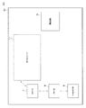
- FIG. 27 is a diagram schematically showing an example of the arrangement of components in the ONU according to the second embodiment of the present invention.
- the ONU 212 includes a parent substrate B11.
- An optical transceiver 111, a MAC-IC 31, a PHY-IC 32, a LAN connector 33, and a power supply circuit 34 are mounted on the parent substrate B11.
- the ONU 212 has a configuration that does not include a child board, and the optical transceiver 111 is directly mounted on the parent board B11.
- the MAC-IC 31, the PHY-IC 32, and the LAN connector 33 correspond to units other than the optical transceiver 101 among the units of the ONU 202 shown in FIG.
- the power supply circuit 34 supplies power to each unit in the ONU 212.
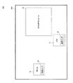
- FIG. 28 is a diagram schematically showing an example of the arrangement of each component in the optical transceiver according to the second embodiment of the present invention.
- optical transceiver 111 CPU 11, TRX-IC 12, and BOSA optical module 13 are covered with metal shield SD1.
- the distance between the temperature sensor 21 and the BOSA optical module 13 is equal to or less than the distance between the TRX-IC 12 and the BOSA optical module 13.
- the CPU 11 is arranged in the vicinity of the BOSA optical module 13 and at a position away from the TRX-IC 12.
- the arrangement direction of the TRX-IC 12 and the BOSA optical module 13 intersects with the arrangement direction of the CPU 11 and the BOSA optical module 13.
- the TRX-IC 12 and the BOSA optical module 13 are arranged near both ends in the longitudinal direction of the metal shield SD1, respectively, and the CPU 11 is located near the middle portion in the longitudinal direction and one end portion in the short direction of the metal shield SD1. Has been placed.
- the same control of the reverse bias voltage Vapd as that of the optical transceiver 101 according to the first embodiment of the present invention can be applied to the optical transceiver 111 having such an arrangement.
- the distance between the temperature sensor 21 and the BOSA optical module 13 is equal to or less than the distance between the transmission driver DV and the BOSA optical module 13.
- the temperature sensor 21 and the BOSA optical module 13 are brought close to each other, and in the configuration in which the temperature sensor 21 can simulate the temperature of the BOSA optical module 13 more accurately, the influence of the BOSA optical module 13 by the transmission driver DV is accurately grasped.
- the reverse bias voltage Vapd to the light receiving element PD can be favorably adjusted according to the temperature of the light receiving element PD.
- a temperature sensor An integrated circuit capable of performing arithmetic processing using the temperature detected by the temperature sensor;
- An optical module including a light emitting element and a light receiving element;
- a transmission driver for driving the light emitting element; Housing the temperature sensor, the integrated circuit, the optical module, and the transmission driver, and having a thermally conductive housing;
- the difference between the detected temperature of the temperature sensor in the optical signal transmission on state by the light emitting element and the detected temperature of the temperature sensor in the optical signal transmission off state is greater than 2 ° C.
- the power consumption of the transmission driver is greater than the power consumption of the integrated circuit and the power consumption of the optical module
- the integrated circuit includes the temperature sensor;
- the light receiving element can change the multiplication factor by a bias voltage,
- the optical signal is a burst optical signal, An optical transceiver used in a home device in a PON system.
- the driving rate of the transmission driver is a,
- the detected temperature of the first temperature sensor is T1,
- the detected temperature of the second temperature sensor is T2
- the temperature of the light receiving part of the optical module is Tr
- the temperature error allowed for the control of the light receiving unit in the optical module is Terr, In a state where the ambient temperature of the housing in a light-on state of transmission of the optical signal by the light emitting element is a predetermined temperature,
- the value of Tr that can be estimated from T1 and T2 when a is the minimum value is Tmin,
- When the value of Tr that can be estimated from T1 and T2 when a is the maximum value is Tmax,
- a light emitting element A transmission driver for driving the light emitting element; A light receiving element capable of changing the multiplication factor by the bias voltage; A temperature sensor; A calculation unit for calculating a driving rate of the transmission driver; An adjustment unit for adjusting the bias voltage to the light receiving element, The adjusting unit is configured to perform linear calculation using a plurality of target values of the bias voltage in a combination of a plurality of temperatures and a plurality of the driving rates based on the detection temperature of the temperature sensor and the calculation result of the driving rate.
- Adjust the bias voltage further, A storage unit that stores a correspondence relationship between the target value of the bias voltage and the temperature for each driving rate; The adjustment of the bias voltage by the adjustment unit is performed based on the plurality of target values corresponding to the detected temperature of the temperature sensor in the correspondence relationship, and the calculation result of the drive rate, A burst-like optical signal is transmitted by the light emitting element, The driving rate is a duty ratio of a burst of the optical signal, An optical communication device that is a home device in a PON system.
Landscapes
- Physics & Mathematics (AREA)
- Electromagnetism (AREA)
- Engineering & Computer Science (AREA)
- Computer Networks & Wireless Communication (AREA)
- Signal Processing (AREA)
- Optics & Photonics (AREA)
- Nonlinear Science (AREA)
- Optical Communication System (AREA)
- Light Receiving Elements (AREA)
Abstract
Description
図1は、本発明の第1の実施の形態に係るPONシステムの構成を示す図である。
バイアス制御部83は、固定電圧たとえば電源電圧Vccの供給される電源ノードに接続され、受光素子PDにバイアス電圧を供給する。バイアス制御部83は、バイアス電圧の調整機能を有する。
Vapd=K1×Vctrl+K2 ・・・(B1)
Vctrl=Ictrl×Ra ・・・(B2)
Iapd=M×RS1×Pin1 ・・・(C1)
(2)次に、送信オフ状態において、増倍率Mが最適値となる逆バイアス電圧Vapdを生成するためにCPU11におけるD/Aコンバータに与える制御デジタル値を複数の温度で記録し、温度と制御デジタル値との関係を直線近似する。
(3)次に、バースト光信号のバーストのデューティ比を計算する。具体的には、積分回路84を用いてバースト制御信号を積分する。
(4)次に、デューティ比を変数とする線形演算によって制御デジタル値を決定する。
制御デジタル値=y31+(x31-y31)×0.1
制御デジタル値=y15+(x15-y15)×0.8
制御デジタル値=B+(A-B)×a
Tr=1.0157×Ta+9.5013
Tl=0.9906×Ta+22.413
Tc=1.0289×Ta+17.701
Tr=2.4163×Tc-1.4844×Tl ・・・(1)
Trd=0.9911×Ta+6.627
Tld=1.0027×Ta+8.3841
Tcd=0.9877×Ta+8.1261
Trd=12.52181×Tcd-11.3461×Tld ・・・(2)
Tcd=0.959957×Tc-8.866103 ・・・(3)
Tld=1.012215×Tl-14.30268 ・・・(4)
Trd=12.0204×Tc-11.48469×Tl+51.25998 ・・・(5)
Tr-Trd=-9.6041×Tc+10.00029×Tl+51.25998 ・・・(6)
Tr_a=Trd+a×(Tr-Trd) ・・・(7)
Tr_a=(12.0204-9.6041×a)×Tc+(-11.48469+10.00029×a)×Tl+(1-a)×51.25998
Tr_a=(2.132436+0.618751×a)×Tc-(1.1555+0.6018×a)×Tl+(a-1)×6.793542
本実施の形態は、第1の実施の形態に係るONUと比べて配置を変更したONUに関する。以下で説明する内容以外は第1の実施の形態に係るONUと同様である。
温度センサと、
前記温度センサの検出温度を用いた演算処理を行なうことが可能な集積回路と、
発光素子および受光素子を含む光モジュールと、
前記発光素子を駆動する送信ドライバと、
前記温度センサ、前記集積回路、前記光モジュールおよび前記送信ドライバを収容し、熱伝導性を有する筐体とを備え、
前記発光素子による光信号の送信オン状態における前記温度センサの検出温度と前記光信号の送信オフ状態における前記温度センサの検出温度との差が2℃より大きく、
前記送信ドライバの消費電力は、前記集積回路の消費電力および前記光モジュールの消費電力より大きく、
前記集積回路は、前記温度センサを含み、
前記受光素子は、バイアス電圧による増倍率の変更が可能であり、
前記光信号は、バースト状の光信号であり、
PONシステムにおける宅側装置に用いられる、光トランシーバ。
第1の温度センサと、
第2の温度センサと、
発光素子および受光素子を含む光モジュールと、
前記第2の温度センサが熱的に結合され、前記発光素子を駆動する送信ドライバと、
前記第1の温度センサ、前記第2の温度センサ、前記光モジュールおよび前記送信ドライバを収納し、熱伝導性を有する筐体とを備え、
前記送信ドライバの駆動率をaとし、
前記第1の温度センサの検出温度をT1とし、
前記第2の温度センサの検出温度をT2とし、
前記光モジュールの受光部の温度をTrとし、
前記光モジュールにおける受光部の制御のために許容される温度誤差をTerrとし、
前記発光素子による光信号の送信オン状態における前記筐体の周囲温度が所定温度である状態において、
aが最小値であるときのT1およびT2から推定できるTrの値をTminとし、
aが最大値であるときのT1およびT2から推定できるTrの値をTmaxとすると、
aが前記最小値および前記最大値の中間値であるときにTminおよびTmaxをaで内分することによって求まるTrの推定値に対する、Trの実測値の誤差がTerr以下であり、
前記受光素子は、バイアス電圧による増倍率の変更が可能であり、
前記光信号は、バースト状の光信号であり、
PONシステムにおける宅側装置に用いられる、光トランシーバ。
発光素子と、
前記発光素子を駆動する送信ドライバと、
バイアス電圧による増倍率の変更が可能な受光素子と、
温度センサと、
前記送信ドライバの駆動率を算出する演算部と、
前記受光素子への前記バイアス電圧を調整する調整部とを備え、
前記調整部は、前記温度センサの検出温度および前記駆動率の算出結果に基づいて、複数の温度かつ複数の前記駆動率の組み合わせにおける、前記バイアス電圧の複数の目標値を用いた線形演算によって前記バイアス電圧の調整を行い、
さらに、
前記バイアス電圧の目標値と温度との前記駆動率ごとの対応関係を記憶する記憶部を備え、
前記調整部による前記バイアス電圧の調整は、前記対応関係において前記温度センサの検出温度に対応する複数の前記目標値、および前記駆動率の算出結果に基づいて行われ、
前記発光素子によりバースト状の光信号が送信され、
前記駆動率は、前記光信号のバーストのデューティ比であり、
PONシステムにおける宅側装置である、光通信装置。
12 TRX-IC
13 BOSA光モジュール
14 抵抗
15 DC/DCコンバータ
16 コネクタ
21,22 温度センサ
23 記憶部
31 MAC-IC
32 PHY-IC
33 LANコネクタ
34 電源回路
36 バイアス制限部
81 TIA
82 LIA
83 バイアス制御部(調整部)
84 積分回路(演算部)
85 出力バッファ
86 プリアンプ
87 出力バッファ回路(変調電流供給回路)
88 バイアス電流供給回路
89 発光回路
92 PON受信処理部
93 バッファメモリ
94 UN送信処理部
95 UNIポート
96 UN受信処理部
97 バッファメモリ
98 PON送信処理部
99 制御部
101,111 光トランシーバ
151 バースト送信部
152 受信部
201 局側装置
202,202A,202B,202C,212 ONU
301 PONシステム
B1 子基板
B11 親基板
SD1 金属シールド
SP スプリッタ
OPTF 光ファイバ
LD 発光素子
L1,L2 インダクタ
PD 受光素子
Claims (6)
- 温度センサと、
前記温度センサの検出温度を用いた演算処理を行なうことが可能な集積回路と、
発光素子および受光素子を含む光モジュールと、
前記発光素子を駆動する送信ドライバと、
前記温度センサ、前記集積回路、前記光モジュールおよび前記送信ドライバを収容し、熱伝導性を有する筐体とを備え、
前記発光素子による光信号の送信オン状態における前記温度センサの検出温度と前記光信号の送信オフ状態における前記温度センサの検出温度との差が2℃より大きく、
前記送信ドライバの消費電力は、前記集積回路の消費電力および前記光モジュールの消費電力より大きい、光トランシーバ。 - 前記送信ドライバは、前記温度センサと前記光モジュールとの間に配置されている、請求項1に記載の光トランシーバ。
- 前記温度センサおよび前記光モジュール間の距離が前記送信ドライバおよび前記光モジュール間の距離以下である、請求項1に記載の光トランシーバ。
- 第1の温度センサと、
第2の温度センサと、
発光素子および受光素子を含む光モジュールと、
前記第2の温度センサが熱的に結合され、前記発光素子を駆動する送信ドライバと、
前記第1の温度センサ、前記第2の温度センサ、前記光モジュールおよび前記送信ドライバを収納し、熱伝導性を有する筐体とを備え、
前記送信ドライバの駆動率をaとし、
前記第1の温度センサの検出温度をT1とし、
前記第2の温度センサの検出温度をT2とし、
前記光モジュールの受光部の温度をTrとし、
前記光モジュールにおける受光部の制御のために許容される温度誤差をTerrとし、
前記発光素子による光信号の送信オン状態における前記筐体の周囲温度が所定温度である状態において、
aが最小値であるときのT1およびT2から推定できるTrの値をTminとし、
aが最大値であるときのT1およびT2から推定できるTrの値をTmaxとすると、
aが前記最小値および前記最大値の中間値であるときにTminおよびTmaxをaで内分することによって求まるTrの推定値に対する、Trの実測値の誤差がTerr以下である、光トランシーバ。 - 発光素子と、
前記発光素子を駆動する送信ドライバと、
バイアス電圧による増倍率の変更が可能な受光素子と、
温度センサと、
前記送信ドライバの駆動率を算出する演算部と、
前記受光素子への前記バイアス電圧を調整する調整部とを備え、
前記調整部は、前記温度センサの検出温度および前記駆動率の算出結果に基づいて、複数の温度かつ複数の前記駆動率の組み合わせにおける、前記バイアス電圧の複数の目標値を用いた線形演算によって前記バイアス電圧を調整する、光通信装置。 - 発光素子と、前記発光素子を駆動する送信ドライバと、バイアス電圧による増倍率の変更が可能な受光素子と、温度センサとを備える光通信装置における受光素子の制御方法であって、
前記送信ドライバの駆動率を算出するステップと、
前記受光素子への前記バイアス電圧を調整するステップとを含み、
前記バイアス電圧を調整するステップにおいて、前記温度センサの検出温度および前記駆動率の算出結果に基づいて、複数の温度かつ複数の前記駆動率の組み合わせにおける、前記バイアス電圧の複数の目標値を用いた線形演算によって前記バイアス電圧を調整する、受光素子の制御方法。
Priority Applications (2)
| Application Number | Priority Date | Filing Date | Title |
|---|---|---|---|
| US15/543,303 US10291330B2 (en) | 2015-04-20 | 2016-01-05 | Optical transceiver, optical communication apparatus, and method of controlling light receiving element |
| CA2983175A CA2983175A1 (en) | 2015-04-20 | 2016-01-05 | Optical transceiver, optical communication apparatus, and method of controlling light receiving element |
Applications Claiming Priority (2)
| Application Number | Priority Date | Filing Date | Title |
|---|---|---|---|
| JP2015-085659 | 2015-04-20 | ||
| JP2015085659A JP2016208170A (ja) | 2015-04-20 | 2015-04-20 | 光トランシーバ、光通信装置、および受光素子の制御方法 |
Publications (1)
| Publication Number | Publication Date |
|---|---|
| WO2016170801A1 true WO2016170801A1 (ja) | 2016-10-27 |
Family
ID=57143790
Family Applications (1)
| Application Number | Title | Priority Date | Filing Date |
|---|---|---|---|
| PCT/JP2016/050087 Ceased WO2016170801A1 (ja) | 2015-04-20 | 2016-01-05 | 光トランシーバ、光通信装置、および受光素子の制御方法 |
Country Status (4)
| Country | Link |
|---|---|
| US (1) | US10291330B2 (ja) |
| JP (1) | JP2016208170A (ja) |
| CA (1) | CA2983175A1 (ja) |
| WO (1) | WO2016170801A1 (ja) |
Cited By (1)
| Publication number | Priority date | Publication date | Assignee | Title |
|---|---|---|---|---|
| CN114679218A (zh) * | 2022-03-16 | 2022-06-28 | 新华三技术有限公司 | 一种光模块功耗确定方法及装置 |
Families Citing this family (10)
| Publication number | Priority date | Publication date | Assignee | Title |
|---|---|---|---|---|
| KR102733464B1 (ko) * | 2016-11-22 | 2024-11-25 | 삼성전자주식회사 | 전자 장치 및 그 제어 방법 |
| US10345144B2 (en) * | 2017-07-11 | 2019-07-09 | Bae Systems Information And Electronics Systems Integration Inc. | Compact and athermal VNIR/SWIR spectrometer |
| CN109450554A (zh) * | 2018-10-18 | 2019-03-08 | 成都优博创通信技术股份有限公司 | 激光发射系统和波长漂移的补偿方法 |
| JP2020077956A (ja) * | 2018-11-07 | 2020-05-21 | 住友電気工業株式会社 | 光受信回路 |
| US12387018B2 (en) * | 2020-10-29 | 2025-08-12 | Hewlett Packard Enterprise Development Lp | Behavior model of photodetectors with a built-in lookup table |
| JP7639586B2 (ja) * | 2021-07-06 | 2025-03-05 | 住友電気工業株式会社 | 受信回路 |
| US20230030875A1 (en) * | 2021-07-28 | 2023-02-02 | Hewlett Packard Enterprise Development Lp | Photodetector behavior modeling |
| CN115810923A (zh) * | 2021-09-14 | 2023-03-17 | 华硕电脑股份有限公司 | 可拆式天线以及电子装置 |
| CN115001523B (zh) * | 2022-05-25 | 2023-07-07 | 成都亿芯源半导体科技有限公司 | 基于epon搭配eml的10g速率olt端收发一体芯片 |
| WO2024260274A1 (zh) * | 2023-06-21 | 2024-12-26 | 青岛海信宽带多媒体技术有限公司 | 光模块 |
Citations (4)
| Publication number | Priority date | Publication date | Assignee | Title |
|---|---|---|---|---|
| US20050006567A1 (en) * | 2002-02-12 | 2005-01-13 | James Stewart | Method for calibrating an optoelectronic device based on APD breakdown voltage |
| JP2006222868A (ja) * | 2005-02-14 | 2006-08-24 | Murata Mfg Co Ltd | 光送受信モジュールおよびそれを備えた光送受信装置 |
| JP2006302967A (ja) * | 2005-04-15 | 2006-11-02 | Sumitomo Electric Ind Ltd | 光モジュール |
| JP2009105489A (ja) * | 2007-10-19 | 2009-05-14 | Sumitomo Electric Ind Ltd | 光トランシーバ及び光トランシーバの制御方法 |
Family Cites Families (1)
| Publication number | Priority date | Publication date | Assignee | Title |
|---|---|---|---|---|
| JP2007074397A (ja) * | 2005-09-07 | 2007-03-22 | Sumitomo Electric Ind Ltd | 光受信器 |
-
2015
- 2015-04-20 JP JP2015085659A patent/JP2016208170A/ja active Pending
-
2016
- 2016-01-05 US US15/543,303 patent/US10291330B2/en active Active
- 2016-01-05 CA CA2983175A patent/CA2983175A1/en not_active Abandoned
- 2016-01-05 WO PCT/JP2016/050087 patent/WO2016170801A1/ja not_active Ceased
Patent Citations (4)
| Publication number | Priority date | Publication date | Assignee | Title |
|---|---|---|---|---|
| US20050006567A1 (en) * | 2002-02-12 | 2005-01-13 | James Stewart | Method for calibrating an optoelectronic device based on APD breakdown voltage |
| JP2006222868A (ja) * | 2005-02-14 | 2006-08-24 | Murata Mfg Co Ltd | 光送受信モジュールおよびそれを備えた光送受信装置 |
| JP2006302967A (ja) * | 2005-04-15 | 2006-11-02 | Sumitomo Electric Ind Ltd | 光モジュール |
| JP2009105489A (ja) * | 2007-10-19 | 2009-05-14 | Sumitomo Electric Ind Ltd | 光トランシーバ及び光トランシーバの制御方法 |
Cited By (1)
| Publication number | Priority date | Publication date | Assignee | Title |
|---|---|---|---|---|
| CN114679218A (zh) * | 2022-03-16 | 2022-06-28 | 新华三技术有限公司 | 一种光模块功耗确定方法及装置 |
Also Published As
| Publication number | Publication date |
|---|---|
| US10291330B2 (en) | 2019-05-14 |
| US20180006728A1 (en) | 2018-01-04 |
| CA2983175A1 (en) | 2016-10-27 |
| JP2016208170A (ja) | 2016-12-08 |
Similar Documents
| Publication | Publication Date | Title |
|---|---|---|
| JP2016208170A (ja) | 光トランシーバ、光通信装置、および受光素子の制御方法 | |
| US9525480B2 (en) | Optical communication module, optical network unit, and method of controlling light-emitting element | |
| JP5382375B2 (ja) | 駆動回路および宅側装置 | |
| CN100365885C (zh) | 激光驱动电路和系统 | |
| JP5306547B2 (ja) | レーザダイオード駆動回路 | |
| CN1905431B (zh) | 用于实现突发模式光功率测量的方法和系统 | |
| JP2012142822A (ja) | 光受信装置および光送信装置 | |
| EP2283592A2 (en) | Method and apparatus for controlling the optical output power from a burst mode laser | |
| JP6315950B2 (ja) | 光パワーモニタ用回路、光モジュール、局側装置、光パワーモニタ方法及びプログラム | |
| EP3573258B1 (en) | Passive optical network system, and optical component and matching impedance adjustment method therefor | |
| CN102209410B (zh) | 一种外置突发自动光功率控制电路 | |
| US20140029635A1 (en) | Laser power control using bias and modulation current feedback | |
| JP2010166216A (ja) | 前置増幅器 | |
| Rosales et al. | 50G-PON Downstream Link up to 40 km With a 1342 nm Integrated EML+ SOA | |
| JP6575648B2 (ja) | 光トランシーバ、光通信装置、および受光素子の制御方法 | |
| JP6248581B2 (ja) | 光通信モジュール、光通信装置および光通信方法 | |
| US9948400B2 (en) | Drive circuit and optical network unit | |
| CN105580222A (zh) | 光发射系统 | |
| US9306674B1 (en) | Field-tunable devices for optical communication | |
| TWI506970B (zh) | Optical network terminal network device and method for adjusting optical signal power | |
| JP2014093759A (ja) | 光通信モジュール、通信装置、受光素子のバイアス電圧調整方法および受光素子の増倍率測定方法 | |
| TW200427161A (en) | Laser driver circuit and system | |
| JP5928294B2 (ja) | 回路モジュールおよび光通信装置 | |
| JP2011253843A (ja) | 半導体レーザ駆動装置及び光通信装置 | |
| JP5939032B2 (ja) | 光通信モジュールおよび宅側装置 |
Legal Events
| Date | Code | Title | Description |
|---|---|---|---|
| 121 | Ep: the epo has been informed by wipo that ep was designated in this application |
Ref document number: 16782823 Country of ref document: EP Kind code of ref document: A1 |
|
| WWE | Wipo information: entry into national phase |
Ref document number: 15543303 Country of ref document: US |
|
| ENP | Entry into the national phase |
Ref document number: 2983175 Country of ref document: CA |
|
| NENP | Non-entry into the national phase |
Ref country code: DE |
|
| 122 | Ep: pct application non-entry in european phase |
Ref document number: 16782823 Country of ref document: EP Kind code of ref document: A1 |