WO2016167228A1 - 感光性導電フィルム、導電パターンの形成方法、導電パターン付き基材、及びタッチパネルセンサ - Google Patents
感光性導電フィルム、導電パターンの形成方法、導電パターン付き基材、及びタッチパネルセンサ Download PDFInfo
- Publication number
- WO2016167228A1 WO2016167228A1 PCT/JP2016/061728 JP2016061728W WO2016167228A1 WO 2016167228 A1 WO2016167228 A1 WO 2016167228A1 JP 2016061728 W JP2016061728 W JP 2016061728W WO 2016167228 A1 WO2016167228 A1 WO 2016167228A1
- Authority
- WO
- WIPO (PCT)
- Prior art keywords
- photosensitive
- conductive
- conductive film
- film
- conductive pattern
- Prior art date
- Legal status (The legal status is an assumption and is not a legal conclusion. Google has not performed a legal analysis and makes no representation as to the accuracy of the status listed.)
- Ceased
Links
Images


Classifications
-
- G—PHYSICS
- G06—COMPUTING OR CALCULATING; COUNTING
- G06F—ELECTRIC DIGITAL DATA PROCESSING
- G06F3/00—Input arrangements for transferring data to be processed into a form capable of being handled by the computer; Output arrangements for transferring data from processing unit to output unit, e.g. interface arrangements
- G06F3/01—Input arrangements or combined input and output arrangements for interaction between user and computer
- G06F3/03—Arrangements for converting the position or the displacement of a member into a coded form
- G06F3/041—Digitisers, e.g. for touch screens or touch pads, characterised by the transducing means
- G06F3/044—Digitisers, e.g. for touch screens or touch pads, characterised by the transducing means by capacitive means
- G06F3/0446—Digitisers, e.g. for touch screens or touch pads, characterised by the transducing means by capacitive means using a grid-like structure of electrodes in at least two directions, e.g. using row and column electrodes
-
- G—PHYSICS
- G03—PHOTOGRAPHY; CINEMATOGRAPHY; ANALOGOUS TECHNIQUES USING WAVES OTHER THAN OPTICAL WAVES; ELECTROGRAPHY; HOLOGRAPHY
- G03F—PHOTOMECHANICAL PRODUCTION OF TEXTURED OR PATTERNED SURFACES, e.g. FOR PRINTING, FOR PROCESSING OF SEMICONDUCTOR DEVICES; MATERIALS THEREFOR; ORIGINALS THEREFOR; APPARATUS SPECIALLY ADAPTED THEREFOR
- G03F7/00—Photomechanical, e.g. photolithographic, production of textured or patterned surfaces, e.g. printing surfaces; Materials therefor, e.g. comprising photoresists; Apparatus specially adapted therefor
- G03F7/004—Photosensitive materials
-
- G—PHYSICS
- G03—PHOTOGRAPHY; CINEMATOGRAPHY; ANALOGOUS TECHNIQUES USING WAVES OTHER THAN OPTICAL WAVES; ELECTROGRAPHY; HOLOGRAPHY
- G03F—PHOTOMECHANICAL PRODUCTION OF TEXTURED OR PATTERNED SURFACES, e.g. FOR PRINTING, FOR PROCESSING OF SEMICONDUCTOR DEVICES; MATERIALS THEREFOR; ORIGINALS THEREFOR; APPARATUS SPECIALLY ADAPTED THEREFOR
- G03F7/00—Photomechanical, e.g. photolithographic, production of textured or patterned surfaces, e.g. printing surfaces; Materials therefor, e.g. comprising photoresists; Apparatus specially adapted therefor
- G03F7/004—Photosensitive materials
- G03F7/027—Non-macromolecular photopolymerisable compounds having carbon-to-carbon double bonds, e.g. ethylenic compounds
- G03F7/028—Non-macromolecular photopolymerisable compounds having carbon-to-carbon double bonds, e.g. ethylenic compounds with photosensitivity-increasing substances, e.g. photoinitiators
- G03F7/029—Inorganic compounds; Onium compounds; Organic compounds having hetero atoms other than oxygen, nitrogen or sulfur
-
- G—PHYSICS
- G06—COMPUTING OR CALCULATING; COUNTING
- G06F—ELECTRIC DIGITAL DATA PROCESSING
- G06F3/00—Input arrangements for transferring data to be processed into a form capable of being handled by the computer; Output arrangements for transferring data from processing unit to output unit, e.g. interface arrangements
- G06F3/01—Input arrangements or combined input and output arrangements for interaction between user and computer
- G06F3/03—Arrangements for converting the position or the displacement of a member into a coded form
- G06F3/041—Digitisers, e.g. for touch screens or touch pads, characterised by the transducing means
-
- G—PHYSICS
- G06—COMPUTING OR CALCULATING; COUNTING
- G06F—ELECTRIC DIGITAL DATA PROCESSING
- G06F3/00—Input arrangements for transferring data to be processed into a form capable of being handled by the computer; Output arrangements for transferring data from processing unit to output unit, e.g. interface arrangements
- G06F3/01—Input arrangements or combined input and output arrangements for interaction between user and computer
- G06F3/03—Arrangements for converting the position or the displacement of a member into a coded form
- G06F3/041—Digitisers, e.g. for touch screens or touch pads, characterised by the transducing means
- G06F3/044—Digitisers, e.g. for touch screens or touch pads, characterised by the transducing means by capacitive means
Definitions
- the present invention relates to a photosensitive conductive film, a method for forming a conductive pattern, a substrate with a conductive pattern, and a touch panel sensor.
- Liquid crystal display elements or touch panel sensors are used in large electronic devices such as personal computers and televisions, small electronic devices such as car navigation, mobile phones, and electronic dictionaries, and display devices such as OA devices and FA devices. These liquid crystal display elements and touch panel sensors require a transparent electrode material.
- capacitive touch panels In a capacitive touch panel, when a fingertip (conductor) contacts the touch input surface, the fingertip and the conductive film are capacitively coupled to form a capacitor. The capacitive touch panel detects the coordinates by capturing the change in charge at the contact position of the fingertip.
- the projected capacitive touch panel has good operability because it can detect multiple points of the fingertip and can give complicated instructions. Due to its good operability, a projected capacitive touch panel is increasingly used as an input device on a display surface in a device having a small display device such as a mobile phone and a portable music player.
- a plurality of X electrodes and a plurality of Y electrodes perpendicular to the X electrodes form a two-layer structure in order to express two-dimensional coordinates based on the X and Y axes. is doing.
- a transparent electrode material is used for these electrodes.
- Patent Document 1 proposes a method for forming a conductive pattern using a photosensitive conductive film having a photosensitive layer containing conductive fibers. If this technique is used, a conductive pattern can be easily formed directly on various substrates by a photolithography process.
- An object of the present invention is to provide a photosensitive conductive film capable of forming a conductive pattern containing conductive fibers with sufficient resolution, a method for forming the conductive pattern, a substrate with a conductive pattern having a conductive pattern with excellent resolution, and An object is to provide a touch panel.
- the present inventor has found that the resolution can be improved by blending a photosensitive layer containing conductive fibers with an ultraviolet absorber, and the present invention has been completed.
- the present invention comprises a support film and a photosensitive layer provided on the support film, the photosensitive layer comprising conductive fibers, a binder polymer, a photopolymerizable compound, a photopolymerization initiator, and an ultraviolet absorber.
- a photosensitive conductive film is provided.
- a conductive pattern containing conductive fibers can be formed with sufficient resolution. This is presumably because the photosensitive layer has the above composition containing an ultraviolet absorber, so that the scattered light generated by the conductive fibers is absorbed during patterning, and the influence of halation can be reduced.
- the ultraviolet absorber may have a maximum absorption wavelength in a wavelength range of 250 nm to 400 nm. Such an ultraviolet absorber can effectively absorb the scattered light from the conductive fiber, and can further suppress a reduction in resolution to a higher degree.
- the photosensitive conductive film may have a minimum visible light transmittance of 85% or more at 400 to 700 nm. When the minimum value of the visible light transmittance is in the above range, it is possible to provide a conductive pattern which is not colored and has excellent transparency.
- the ultraviolet absorber may have a thermally polymerizable group or a photopolymerizable group. When such an ultraviolet absorber is used, the bleeding of the ultraviolet absorber from the photosensitive layer or a cured product thereof can be further suppressed.
- the ultraviolet absorber may be a polymer type ultraviolet absorber. When such an ultraviolet absorber is used, the bleeding of the ultraviolet absorber from the photosensitive layer or a cured product thereof can be further suppressed.
- the conductive fiber may be a silver fiber.
- a photosensitive conductive film having high visible light transmittance in the wavelength region of 400 nm to 700 nm and high conductivity can be provided.
- the present invention also includes a step of transferring the photosensitive layer of the photosensitive conductive film of the present invention onto a substrate, an exposure step of irradiating the photosensitive layer transferred onto the substrate with actinic rays in a pattern, and the above And a development step of forming a conductive pattern by removing an unexposed portion of the photosensitive layer.
- a conductive pattern can be formed with sufficient resolution even in the case of a photosensitive layer containing conductive fibers. According to the method for forming the conductive pattern, the conductive pattern can be easily formed on the substrate.
- the present invention also provides a substrate with a conductive pattern, which has a substrate and a conductive pattern formed on the substrate by the method for forming a conductive pattern of the present invention.
- the substrate with a conductive pattern of the present invention has a conductive pattern formed by the above-described method for forming a conductive pattern, a conductive pattern with excellent resolution, that is, a thinner conductive pattern and a thinner space portion (photosensitive layer removal) Part).
- the present invention also provides a touch panel sensor comprising the substrate with a conductive pattern of the present invention.
- the touch panel sensor of the present invention includes the above-described substrate with a conductive pattern, the pattern appearance of the conductive pattern can be reduced, and the visibility can be improved (the pattern is difficult to see).
- a photosensitive conductive film capable of forming a conductive pattern containing conductive fibers with sufficient resolution, a method for forming a conductive pattern, a substrate with a conductive pattern having a conductive pattern with excellent resolution, and A touch panel can be provided.
- (meth) acrylate in the present specification means “acrylate” or “methacrylate”.
- (meth) acrylic acid means “acrylic acid” or “methacrylic acid”
- (meth) acryloyl group means “acryloyl group” or “methacryloyl group”.
- a numerical range indicated by using “to” indicates a range including the numerical values described before and after “to” as the minimum value and the maximum value, respectively.
- “A or B” only needs to include one of A and B, or may include both.
- the exemplary materials may be used alone or in combination of two or more unless otherwise specified.
- the photosensitive conductive film according to the present embodiment includes a support film and a photosensitive layer provided on the support film, and the photosensitive layer includes conductive fibers, a binder polymer, a photopolymerizable compound, and a photopolymerization initiator. , And an ultraviolet absorber.
- One embodiment of the photosensitive conductive film is shown in FIG.
- the photosensitive conductive film 10 includes a support film 1, a photosensitive layer 4, and a protective film 5, and the photosensitive layer 4 includes a conductive film 2 and a photosensitive resin layer 3.
- the conductive film 2 contains conductive fibers.
- the photosensitive conductive film is used to transfer the photosensitive layer onto the base material and form the photosensitive layer on the base material, it can also be said to be a transfer type photosensitive conductive film.
- the photosensitive conductive film 10 is illustrated so that the boundary between the conductive film 2 and the photosensitive resin layer 3 provided on the conductive film 2 is clear.
- the boundary with the conductive resin layer 3 is not necessarily clear.
- Any conductive film may be used as long as conductivity is obtained in the surface direction of the photosensitive layer, and the conductive resin may be mixed with the photosensitive resin layer.
- the composition constituting the photosensitive resin layer may be impregnated in the conductive film, or the composition constituting the photosensitive resin layer may be present on the surface of the conductive film.
- the support film 1 includes a polymer film having heat resistance and solvent resistance.
- a polymer film having heat resistance and solvent resistance.
- examples of such a polymer film include a polyethylene terephthalate film, a polyethylene film, a polypropylene film, and a polycarbonate film.
- a polyethylene terephthalate film is preferable from the viewpoint of transparency and heat resistance.
- These polymer films may be surface-treated so as to be easily peeled off from the photosensitive layer 4, and are preferably materials that can be easily peeled off from the photosensitive layer 4.
- the thickness of the support film 1 is preferably 5 to 300 ⁇ m, more preferably 10 to 200 ⁇ m, still more preferably 15 to 100 ⁇ m, and particularly preferably 30 to 70 ⁇ m.
- a step of applying a photosensitive resin composition to form a conductive dispersion or a photosensitive resin layer 3 to form the conductive film 2, or a support film before developing the exposed photosensitive resin layer 3 In the step of peeling, from the viewpoint of preventing mechanical strength from being reduced and the support film from being broken, it is preferably 5 ⁇ m or more, more preferably 10 ⁇ m or more, further preferably 15 ⁇ m or more, and 30 ⁇ m. The above is particularly preferable.
- the photosensitive resin layer is irradiated with actinic rays through the support film, it is preferably 300 ⁇ m or less, more preferably 200 ⁇ m or less, and 100 ⁇ m or less. More preferably, it is particularly preferably 70 ⁇ m or less.
- the haze value of the support film 1 is preferably 0.01 to 5.0%, more preferably 0.01 to 3.0%, from the viewpoint of improving sensitivity and resolution. It is more preferably from 2.0% to 2.0%, particularly preferably from 0.01% to 1.0%.
- the haze value can be measured according to JIS K 7375 (established in 2008). It can also be measured with a commercially available turbidimeter such as NDH-1001DP (trade name, manufactured by Nippon Denshoku Industries Co., Ltd.).
- the conductive fiber examples include metal fibers such as gold, silver, copper, and platinum, or carbon fibers such as carbon nanotubes.
- the conductive fiber is easy to prepare, is easy to control the shape of the conductive fiber, has high visible light transmittance in the wavelength range of 400 to 700 nm, and has high conductivity.
- silver fiber is preferable, and silver nanowire is more preferable.
- the nanowire is, for example, a small difference in size between two dimensions (X, Y) (specifically, the difference in size is 5 times or less), and both X and Y are 300 nm or less. This is a size, and indicates a shape in which the size of one remaining dimension (Z) is 10 times or more of X and Y.
- FIG. 2 is a partially cutaway perspective view showing an embodiment of a photosensitive conductive film.
- the conductive film 2 preferably has a network structure in which conductive fibers are in contact with each other like the photosensitive conductive film 12 shown in FIG.
- the conductive film 2 having such a network structure may be formed on the surface of the photosensitive resin layer 3 on the support film 1 side, but on the surface of the photosensitive layer 4 exposed when the support film 1 is peeled off.
- the conductive film 2 may be formed so that a part of the photosensitive resin layer 3 enters the conductive film 2, and the conductive film is formed on the surface layer of the photosensitive resin layer 3 on the support film 1 side. 2 may be included.
- the conductive fibers including silver fibers or silver nanowires can be prepared by, for example, a method of reducing silver ions with a reducing agent such as NaBH 4 or a polyol method.
- the fiber diameter of the conductive fiber is preferably 1 nm to 100 nm, more preferably 2 nm to 50 nm, and further preferably 3 nm to 30 nm.
- the fiber length of the conductive fiber is preferably 1 ⁇ m to 100 ⁇ m, more preferably 2 ⁇ m to 50 ⁇ m, and even more preferably 3 ⁇ m to 10 ⁇ m.
- the fiber diameter and fiber length can be measured with a scanning electron microscope.
- an organic conductor may be used in combination with the conductive fiber.
- the organic conductor can be used without particular limitation, but from the viewpoint of high transparency and conductivity, it is preferable to use an organic conductor such as a polymer of a thiophene derivative and an aniline derivative. Specifically, polyethylenedioxythiophene, polyhexylthiophene, polyaniline, polyvinylpyrrolidone, or the like can be used.
- the thickness of the conductive film 2 varies depending on the use of the conductive pattern formed using the photosensitive conductive film of the present invention and the required conductivity, but is preferably 1 ⁇ m or less, and preferably 1 nm to 0.5 ⁇ m. More preferably, the thickness is 5 nm to 0.1 ⁇ m.
- the thickness of the conductive film 2 is 1 ⁇ m or less, the light transmittance in the wavelength range of 400 to 700 nm is high, the pattern formation is excellent, and it is particularly suitable for the production of a transparent electrode.
- the thickness of the conductive film 2 indicates a value measured by a scanning electron microscope.
- the conductive film 2 is coated on the support film 1 with a conductive dispersion obtained by adding the above-described conductive fiber or organic conductor to water or an organic solvent, a dispersion stabilizer such as a surfactant, and the like, It can be formed by drying. After drying, the conductive film 2 formed on the support film 1 may be laminated as necessary.
- Coating can be performed by a known method such as a roll coating method, a comma coating method, a gravure coating method, an air knife coating method, a die coating method, a bar coating method, or a spray coating method.
- the drying can be performed at 30 to 150 ° C. for about 1 to 30 minutes with a hot air convection dryer or the like.
- the conductive fiber and the organic conductor may coexist with a surfactant or a dispersion stabilizer.
- the surface resistivity of the conductive film 2 and the photosensitive conductive film including the conductive film 2 can be adjusted by the amount of conductive fibers.
- the photosensitive layer only needs to contain an ultraviolet absorber.
- the conductive film is formed using a conductive dispersion containing the ultraviolet absorber, and the ultraviolet absorber is present in the conductive film.
- an ultraviolet absorber may be present in the photosensitive resin layer.
- an ultraviolet absorber can be contained.
- the photosensitive resin layer 3 examples include those formed from a photosensitive resin composition containing (A) a binder polymer, (B) a photopolymerizable compound, and (C) a photopolymerization initiator.
- the photosensitive resin composition may contain the (D) ultraviolet absorber.
- (A) As binder polymer epoxy resin obtained by reaction of acrylic resin, styrene resin, epoxy resin, amide resin, amide epoxy resin, alkyd resin, phenol resin, ester resin, urethane resin, epoxy resin and (meth) acrylic acid Examples thereof include acid-modified epoxy acrylate resins obtained by reaction of acrylate resins and epoxy acrylate resins with acid anhydrides.
- acrylic resin is derived from (meth) acrylic acid and a (meth) acrylic acid alkyl ester as a constituent unit. More preferably.
- acrylic resin means a polymer mainly having a monomer unit derived from a polymerizable monomer having a (meth) acryloyl group.
- acrylic resin one produced by radical polymerization of a polymerizable monomer having a (meth) acryloyl group can be used.
- Examples of the polymerizable monomer having a (meth) acryloyl group include acrylamide such as diacetone acrylamide; (meth) acrylic acid alkyl ester, 2-hydroxyalkyl (meth) acrylate, (meth) acrylic acid tetrahydrofurfuryl ester, ( (Meth) acrylic acid dimethylaminoethyl ester, (meth) acrylic acid diethylaminoethyl ester, (meth) acrylic acid glycidyl ester, (meth) acrylic acid benzyl ester, 2,2,2-trifluoroethyl (meth) acrylate, 2, (Meth) acrylic acid esters such as 2,3,3-tetrafluoropropyl (meth) acrylate; (meth) acrylic acid, ⁇ -bromo (meth) acrylic acid, ⁇ -chloro (meth) acrylic acid, ⁇ -furyl ( (Meth) acrylic acid, ⁇ -styryl (meth)
- the acrylic resin includes styrene derivatives; acrylonitrile; esters of vinyl alcohol such as vinyl-n-butyl ether; maleic acid; maleic anhydride; By copolymerizing monomeric monomers such as monomethyl maleate, monoethyl maleate and monoisopropyl maleate; fumaric acid; cinnamic acid; ⁇ -cyanocinnamic acid; itaconic acid; crotonic acid It may be manufactured.
- (meth) acrylic acid alkyl ester (meth) acrylic acid methyl ester, (meth) acrylic acid ethyl ester, (meth) acrylic acid propyl ester, (meth) acrylic acid butyl ester, (meth) acrylic acid hexyl ester,
- acrylic acid heptyl ester (meth) acrylic acid octyl ester, (meth) acrylic acid 2-ethylhexyl ester, (meth) acrylic acid nonyl ester, and the like.
- the binder polymer preferably has a carboxyl group from the viewpoint of improving alkali developability.
- Examples of the polymerizable monomer having a carboxyl group include (meth) acrylic acid as described above.
- the ratio of the carboxyl group of the binder polymer is preferably 10 to 50% by mass, and preferably 12 to 40% by mass as the ratio of the polymerizable monomer having a carboxyl group to the total polymerizable monomer to be used. Is more preferable, 12 to 30% by mass is further preferable, and 12 to 25% by mass is particularly preferable. In terms of excellent alkali developability, the content is preferably 10% by mass or more, and in terms of excellent alkali resistance, it is preferably 50% by mass or less.
- the binder polymer is preferably a binder polymer having a structural unit based on (meth) acrylic acid and a structural unit based on (meth) acrylic acid methyl ester or a structural unit based on (meth) acrylic acid ethyl ester. Binder polymers having a structural unit based on (meth) acrylic acid, a structural unit based on (meth) acrylic acid methyl ester, and a structural unit based on (meth) acrylic acid ethyl ester are more preferred.
- the weight average molecular weight of the binder polymer is preferably 5000 to 300000, more preferably 20000 to 150,000, and more preferably 30000 to 100,000 from the viewpoint of balancing the mechanical strength and alkali developability. Further preferred. In terms of excellent developer resistance, the weight average molecular weight is preferably 5000 or more. Further, from the viewpoint of development time, it is preferably 300000 or less. In this specification, the weight average molecular weight is a value measured by a gel permeation chromatography method (GPC) and converted by a calibration curve created using standard polystyrene.
- GPC gel permeation chromatography
- the acid value of the binder polymer is preferably 75 to 200 mgKOH / g, more preferably 75 to 150 mgKOH / g, and more preferably 75 to 120 mgKOH / g from the viewpoint of excellent pattern formability. More preferred is 78 to 120 mg KOH / g.
- the acid value of a binder polymer can be measured as follows. First, 1 g of the binder polymer that is the object of acid value measurement is precisely weighed. 30 g of acetone is added to the precisely weighed binder polymer and dissolved uniformly. Next, an appropriate amount of phenolphthalein as an indicator is added to the solution, and titration is performed using a 0.1N aqueous KOH solution. And an acid value is computed by following Formula.
- Acid value 0.1 ⁇ Vf ⁇ 56.1 / (Wp ⁇ I / 100)
- Vf represents the titration amount (mL) of the KOH aqueous solution
- Wp represents the weight (g) of the solution containing the measured binder polymer
- I represents the ratio of the nonvolatile content in the solution containing the measured binder polymer ( Mass%).
- the photopolymerizable compound (B) The photopolymerizable compound will be described.
- the photopolymerizable compound preferably has an ethylenically unsaturated bond.
- Examples of the photopolymerizable compound having an ethylenically unsaturated bond include 2,2-bis (4-((meth) acryloxypolyethoxy) phenyl) propane, 2,2-bis (4-((meth) acryloxypoly).
- Bisphenol A di (meth) acrylate compounds such as propoxy) phenyl) propane, 2,2-bis (4-((meth) acryloxypolyethoxypolypropoxy) phenyl) propane; polyethylene glycol di (meth) acrylate, polypropylene glycol di Polyalkylene glycol di (meth) acrylates such as (meth) acrylate and polyethylene polypropylene glycol di (meth) acrylate; trimethylolpropane di (meth) acrylate, trimethylolpropane tri (meth) acrylate, trimethylolpropane etoxy Trimethylolpropane (meth) acrylates such as tri (meth) acrylate and trimethylolpropane triethoxytri (meth) acrylate; tetramethylolmethane (meta) such as tetramethylolmethane tri (meth) acrylate and tetramethylolmethanetetra (meth
- trimethylolpropane (meth) acrylate or dipentaerythritol (meth) acrylate is preferably used, and trimethylolpropane (meth) acrylate is more preferably used.
- the content ratio of the photopolymerizable compound is preferably 30 to 80% by mass, and more preferably 40 to 70% by mass with respect to 100% by mass of the total of the binder polymer and the photopolymerizable compound. . It is preferably 30% by mass or more in terms of excellent coating properties of the photocurable and photosensitive resin composition, and 80% by mass or less in terms of excellent storage stability when wound as a film. Is preferred.
- the photopolymerization initiator will be described.
- the photopolymerization initiator is not particularly limited as long as the photopolymerization initiator is selected so that the light wavelength of the exposure machine to be used matches the wavelength necessary for function expression.
- Examples of the photopolymerization initiator include benzophenone, N, N, N ′, N′-tetramethyl-4,4′-diaminobenzophenone (Michler ketone), N, N, N ′, N′-tetraethyl-4,4 '-Diaminobenzophenone, 4-methoxy-4'-dimethylaminobenzophenone, 2-benzyl-2-dimethylamino-1- (4-morpholinophenyl) -butanone-1,2-methyl-1- [4- (methylthio) Aromatic ketones such as phenyl] -2-morpholino-propanone-1; benzoin ether compounds such as benzoin methyl ether, benzoin ethyl
- an oxime ester compound or a phosphine oxide compound is preferable because of transparency and pattern forming ability when the photosensitive layer is a thin film (for example, 10 ⁇ m or less).
- Examples of the oxime ester compound include compounds represented by the following general formula (C-1) and general formula (C-2). From the viewpoint of fast curability and transparency, a compound represented by the following general formula (C-1) is preferred.
- R 1 represents an alkyl group having 1 to 12 carbon atoms or a cycloalkyl group having 3 to 20 carbon atoms.
- R 1 is preferably an alkyl group having 3 to 9 carbon atoms.
- the aromatic ring in the general formula (C-1) may have a substituent. Examples of the substituent include a hydrogen atom or an alkyl group having 1 to 12 carbon atoms.
- R 2 represents a hydrogen atom or an alkyl group having 1 to 12 carbon atoms
- R 3 represents an alkyl group having 1 to 12 carbon atoms or a cycloalkyl group having 3 to 20 carbon atoms
- R 4 represents an alkyl group having 1 to 12 carbon atoms
- R 5 represents an alkyl group or aryl group having 1 to 20 carbon atoms
- p1 represents an integer of 0 to 3. When p1 is 2 or more, the plurality of R 4 may be the same or different.
- the carbazole structure may have a substituent as long as the effects of the present invention are not impaired. Examples of the substituent include a hydrogen atom or an alkyl group having 1 to 12 carbon atoms.
- R 2 or R 4 is preferably an alkyl group having 1 to 12 carbon atoms, more preferably an alkyl group having 1 to 8 carbon atoms, and 1 to 4 carbon atoms. More preferably, it is an alkyl group.
- R 3 is preferably an alkyl group having 1 to 8 carbon atoms, or a cycloalkyl group having 4 to 15 carbon atoms, and an alkyl group having 1 to 4 carbon atoms or a carbon number A 4 to 10 cycloalkyl group is more preferable, and a methyl group and an ethyl group are particularly preferable.
- R 5 is preferably an alkyl group having 1 to 12 carbon atoms or an aryl group having 6 to 16 carbon atoms, and an alkyl group having 1 to 8 carbon atoms or 6 to 14 carbon atoms. Are more preferable, and an alkyl group having 1 to 4 carbon atoms or an aryl group having 6 to 12 carbon atoms is more preferable.
- Examples of the compound represented by the general formula (C-1) include 1,2-octanedione-1- [4- (phenylthio) phenyl] -2- (O-benzoyloxime). IRGACURE OXE It is commercially available as 01 (BASF Corporation, trade name).
- Examples of the compound represented by the general formula (C-2) include ethanone, 1- [9-ethyl-6- (2-methylbenzoyl) -9H-carbazol-3-yl]-, 1- (O-acetyl). Oxime) and the like, and is commercially available as IRGACURE OXE 02 (trade name, manufactured by BASF Corporation).
- Examples of the phosphine oxide compound include compounds represented by the following general formula (C-3) and general formula (C-4). From the viewpoint of fast curability and transparency, a compound represented by the following general formula (C-3) is preferred.
- R 6 , R 7 and R 8 each independently represents an alkyl group or aryl group having 1 to 20 carbon atoms.
- R 9 , R 10 and R 11 each independently represents an alkyl group or aryl group having 1 to 20 carbon atoms.
- R 6 , R 7 or R 8 in the general formula (C-3) is an alkyl group having 1 to 20 carbon atoms
- R 9 , R 10 or R 11 in the general formula (C-4) are In the case of an alkyl group having 1 to 20 carbon atoms, the alkyl group may be linear, branched, or cyclic, and the alkyl group preferably has 5 to 10 carbon atoms. .
- R 6 , R 7 or R 8 in the general formula (C-3) is an aryl group
- R 9 , R 10 or R 11 in the general formula (C-4) is an aryl group
- the aryl The group may have a substituent.
- the substituent include an alkyl group having 1 to 6 carbon atoms and an alkoxy group having 1 to 4 carbon atoms.
- R 6 , R 7 , and R 8 are preferably aryl groups.
- R 9 , R 10 and R 11 are preferably aryl groups.
- 2,4,6-trimethyl is used because of the transparency of the formed conductive pattern and the pattern forming ability when the film thickness is reduced (for example, 10 ⁇ m or less).
- Benzoyl-diphenyl-phosphine oxide is preferred.
- 2,4,6-Trimethylbenzoyl-diphenyl-phosphine oxide is commercially available, for example, as LUCIRIN TPO (trade name, manufactured by BASF Corporation).
- bis (2, 4, 6) can be obtained from the transparency of the conductive pattern to be formed and the pattern forming ability when the film thickness is reduced (for example, 10 ⁇ m or less).
- -Trimethylbenzoyl) -phenyl-phosphine oxide is preferred.
- Bis (2,4,6-trimethylbenzoyl) -phenyl-phosphine oxide is commercially available, for example, as Irgacure 819 (trade name, manufactured by BASF Corporation).
- 2,2-dimethoxy-1,2-diphenylethane-1-one may be used as a compound having good transparency and pattern forming ability when the photosensitive layer is thinned. Is preferred. 2,2-dimethoxy-1,2-diphenylethane-1-one is commercially available, for example, as Irgacure 651 (trade name, manufactured by BASF Corporation).
- Photopolymerization initiators are 1,2-octanedione-1- [4- (phenylthio) phenyl] -2- (O-benzoyloxime), ethanone, 1- [9-ethyl-6- (2- Methylbenzoyl) -9H-carbazol-3-yl]-, 1- (O-acetyloxime), 2,4,6-trimethylbenzoyl-diphenyl-phosphine oxide, bis (2,4,6-trimethylbenzoyl) -phenyl It is particularly preferable to use either -phosphine oxide or 2,2-dimethoxy-1,2-diphenylethane-1-one.
- the content ratio of the photopolymerization initiator is preferably 0.1 to 20 parts by mass, more preferably 1 to 10 parts by mass with respect to 100 parts by mass in total of the binder polymer and the photopolymerizable compound. More preferably, it is 1 to 5 parts by mass. In terms of excellent photosensitivity, it is preferably 0.1 parts by mass or more, and in terms of excellent photocurability, it is preferably 20 parts by mass or less.
- the ultraviolet absorber will be described.
- the ultraviolet absorber is excellent in the ability to absorb ultraviolet light having a wavelength of 400 nm or less from the viewpoint of scattered light absorption by the conductive fiber, and has little absorption of visible light having a wavelength of 400 nm or more from the viewpoint of improving transparency. Those are preferred. Specifically, a material having a maximum absorption wavelength in a wavelength range of 250 nm to 400 nm corresponds to this.
- Examples of the ultraviolet absorber include oxybenzophenone compounds, triazole compounds, benzotriazole compounds, salicylic acid ester compounds, benzophenone compounds, diphenyl acrylate compounds, cyanoacrylate compounds, diphenyl cyanoacrylate compounds, nickel complex salts, and the like. Among these, a diphenyl cyanoacrylate compound, a cyanoacrylate compound, or a diphenyl acrylate compound is preferable.
- the ultraviolet absorber is preferably a compound having a reactive group, and more preferably a compound having a thermally polymerizable group or a photopolymerizable group. Increasing the content of the ultraviolet absorber can be expected to improve the effect of the present invention. However, when the content of the ultraviolet absorber is increased, the ultraviolet absorber oozes from the cured resin after patterning. (Bleed out). Bleed-out of the ultraviolet absorber is not preferable because it may cause a decrease in transparency of the cured resin and deterioration of optical properties such as turbidity.
- curing material may adsorb
- the ultraviolet absorber has a reactive group, the ultraviolet absorber is fixed to the cured resin during patterning (for example, it is firmly connected and incorporated into the network of the cured resin by a covalent bond). Therefore, the ultraviolet absorber bleeds out (bleed out) or the movement of the ultraviolet absorber in the cured resin is suppressed. Therefore, even if the content of the ultraviolet absorber is increased, an increase in the resistance value due to the adsorption of the ultraviolet absorber to the conductive fiber surface can be suppressed.
- thermally polymerizable group examples include an epoxy group, a glycidyl group, an isocyanate group, an acetylene group, a maleimide group, and an oxetanyl group.
- photopolymerizable group examples include a (meth) acryloyl group, an allyl group, and a maleimide group.
- the thermopolymerizable group and the photopolymerizable group are not limited to the above examples.
- any ultraviolet absorber having a reactive group that can be polymerized by an active radical, an acid, or a base generated by heat or light can be used without particular limitation. Bleed out or adsorption to the surface of conductive fibers can be suppressed.
- the compounds having a thermally polymerizable group or a photopolymerizable group it has a (meth) acryloyl group which is a photopolymerizable group from the viewpoint of availability and stability in the photosensitive conductive film before curing.
- Compounds are particularly preferred.
- Examples of such an ultraviolet absorber include 2- [2-hydroxy-5- [2- (methacryloyloxy) ethyl] phenyl] -2H-benzotriazole, which is a benzotriazole compound having a (meth) acryloyl group. .
- 2- [2-hydroxy-5- [2- (methacryloyloxy) ethyl] phenyl] -2H-benzotriazole is, for example, RUVA-93 (trade name, manufactured by Otsuka Chemical Co., Ltd.) or DAINSORB T-31 (Yamato (Trade name, manufactured by Kasei Co., Ltd.).
- the ultraviolet absorber is preferably a polymer type ultraviolet absorber.
- the polymer type ultraviolet absorber is an ultraviolet absorber obtained by polymerizing the compound having the above-mentioned heat-reactive group or photopolymerizable group.
- a polymer type ultraviolet absorber is a material having one or more ultraviolet absorption sites in a molecule and a large molecular weight. In the present specification, an ultraviolet absorber having a weight average molecular weight of 3000 or more is referred to as a polymer-type ultraviolet absorber.
- the polymer type ultraviolet absorber is one in which bleeding out is suppressed as compared with a low molecular weight ultraviolet absorber.
- the polymer-type ultraviolet absorber is hardly suppressed from being adsorbed on the surface of the conductive fiber.
- a polymer type ultraviolet absorber photopolymerizability from the point of availability of a compound having a polymerizable reactive group as a raw material, easy adjustment of molecular weight, and wide selection of copolymerization components of the polymer A polymer polymerized using a compound having a (meth) acryloyl group as a raw material is preferred.
- polymer-type ultraviolet absorbers examples include solvent-based RSA series (for example, RSA-0124, RSA-0151, and RSA-0191H; all manufactured by Shannan Synthetic Chemical Co., Ltd.), solvent-based PUVA series (for example, PUVA-30M- 50BA, PUVA-30M-30T, and PUVA-50M-50K; all manufactured by Daiwa Kasei Co., Ltd.), solvent-based RSU series (for example, RSU-0017 and SG-864; all manufactured by Daiwa Kasei Co., Ltd.) Water-based RWU series (for example, MW-022, RWU-0001, and RWU-0109; all manufactured by Daiwa Kasei Co., Ltd.) are commercially available.
- solvent-based RSA series for example, RSA-0124, RSA-0151, and RSA-0191H; all manufactured by Shannan Synthetic Chemical Co., Ltd.
- solvent-based PUVA series for example, PUVA-30M- 50BA,
- water-based New Coat UVA series for example, New Coat UVA-101, New Coat UVA-102, New Coat UVA-103, and New Coat UVA-104
- Solvent-based Vana Resin UVA series for example, Vana Resin UVA-5080, hydroxyl group Introducing vanaresin UVA-5080 (OHV20), vanaresin UVA-55T, high hydroxyl value type vanaresin UVA-55MHB, vanaresin UVA-7075, hydroxylintroducing vanaresin UVA-7075 (OHV20), vanaresin UVA-73T), etc.
- Solvent-based UVA series for example, UVA-935LH and UVA-1935LH
- aqueous-based UVA series for example, UVA-700 and UVA-1700 are commercially available from BASF Corporation.
- the weight average molecular weight of the polymer type ultraviolet absorber is preferably 300,000 or less, more preferably 150,000 or less, and more preferably 100,000 or less from the viewpoint of solubility in a solvent and compatibility with a photosensitive resin composition. More preferably it is. Further, from the viewpoint of preventing bleeding out from the photosensitive conductive film and its cured film, it is preferably 3000 or more, more preferably 5000 or more, and further preferably 10,000 or more. From the viewpoint of balancing the solubility in a solvent, the compatibility with the photosensitive resin composition, and the bleed-out prevention property, it is preferably 3000 to 300000, more preferably 5000 to 150,000, and more preferably 10,000 to 100,000. More preferably.
- the weight average molecular weight is a value measured by a gel permeation chromatography method (GPC) and converted by a calibration curve prepared using standard polystyrene.
- the content ratio of the (D) ultraviolet absorber is preferably 0.1 to 30 parts by mass, and preferably 1 to 20 parts by mass with respect to 100 parts by mass of the total amount of the components (A) and (B). More preferred is 2 to 10 parts by mass.
- the content of the ultraviolet absorber is preferably 0.1 parts by mass or more in terms of effectively suppressing light scattering by the conductive fiber and being excellent in resolution.
- suction to the surface of a conductive fiber, or absorption on the surface of a photosensitive layer in the case of actinic ray irradiation Is preferably 30 parts by mass or less from the viewpoint of suppressing an increase in the amount of photocuring and insufficient internal photocuring.
- a method for incorporating the ultraviolet absorber into the photosensitive layer a method of internally adding in advance into the photosensitive resin composition is common, but the present invention is not limited to the internal addition.
- Other methods for incorporating an ultraviolet absorber in the photosensitive layer include, for example, a method of internally adding an ultraviolet absorber in a conductive fiber dispersion, and a film containing conductive fibers formed on a support film that absorbs ultraviolet rays.
- internal addition to the photosensitive resin composition in advance The method is most preferred.
- an adhesion imparting agent such as a silane coupling agent, a leveling agent, a plasticizer, a filler, an antifoaming agent, a flame retardant, a stabilizer, and an antioxidant.
- a perfume, a thermal crosslinking agent, a polymerization inhibitor and the like can be contained in an amount of about 0.01 to 20 parts by mass with respect to 100 parts by mass of the total amount of the component (A) and the component (B).
- the photosensitive resin layer 3 is a photosensitive resin composition dissolved in a solvent such as methanol, ethanol, acetone, methyl ethyl ketone, methyl cellosolve, ethyl cellosolve, toluene, N, N-dimethylformamide, propylene glycol monomethyl ether, or a mixed solvent thereof.
- a solvent such as methanol, ethanol, acetone, methyl ethyl ketone, methyl cellosolve, ethyl cellosolve, toluene, N, N-dimethylformamide, propylene glycol monomethyl ether, or a mixed solvent thereof.
- This solution can be formed by coating and drying on the support film 1 on which the conductive film 2 is formed.
- the amount of the remaining organic solvent in the photosensitive resin layer after drying is preferably 2% by mass or less in order to prevent the organic solvent from diffusing in the subsequent step.
- the photosensitive resin layer 3 can be applied by a known method such as a roll coating method, a comma coating method, a gravure coating method, an air knife coating method, a die coating method, a bar coating method, or a spray coating method. After coating, drying to remove the organic solvent and the like can be performed at 70 to 150 ° C. for about 5 to 30 minutes with a hot air convection dryer or the like.
- the thickness of the photosensitive resin layer 3 varies depending on the use, but the thickness after drying is preferably 1 to 50 ⁇ m, more preferably 1 to 15 ⁇ m, and further preferably 1 to 10 ⁇ m. If the thickness is less than 1 ⁇ m, coating tends to be difficult, and if it exceeds 50 ⁇ m, the sensitivity due to the decrease in light transmission is insufficient, and the photocuring property of the photosensitive resin layer to be transferred tends to decrease.
- the thickness of the layer (cured film) after curing the photosensitive resin layer 3 is also preferably within these ranges.
- the laminate of the conductive film 2 and the photosensitive resin layer 3 is visible in a wavelength range of 400 nm to 700 nm when the total film thickness of both layers is 1 to 10 ⁇ m.
- the minimum value of light transmittance is preferably 85% or more, and more preferably 90% or more.
- the surface resistivity of the conductive film or the conductive pattern is preferably 1000 ⁇ / ⁇ or less, more preferably 500 ⁇ / ⁇ or less, from the viewpoint of effective utilization as a transparent electrode. Preferably, it is 300 ⁇ / ⁇ or less.
- the surface resistivity can be adjusted by, for example, the concentration of the conductive fiber or the dispersion of the organic conductor or the coating amount.
- the protective film 5 may be laminated so as to be in contact with the surface of the photosensitive resin layer 3 opposite to the support film 1 side.
- a polymer film having heat resistance and solvent resistance such as a polyethylene terephthalate film, a polypropylene film, and a polyethylene film can be used. Further, as the protective film 5, a polymer film similar to the above-described support film may be used.
- the adhesive force between the protective film 5 and the photosensitive layer 4 is such that when the protective film is peeled off and laminated on the substrate from the photosensitive resin layer 3 side, the photosensitive layer is formed in order to make the protective film easy to peel off from the photosensitive layer. It is preferable that it is smaller than the adhesive force between 4 and the support film 1.
- the adhesive force between the protective film 5 and the photosensitive layer 4 is such that when the support film 1 is peeled off and laminated to the base material from the conductive film 2 side, It is preferable that it is larger than the adhesive force between the layer 4 and the support film 1.
- the number of fish eyes with a diameter of 80 micrometers or more contained in a protective film is 5 pieces / m ⁇ 2 > or less.
- “Fisheye” means that materials are melted, kneaded, extruded, biaxially stretched, casting materials, etc., and foreign materials, undissolved materials, oxidized degradation products, etc. are taken into the film. It is a thing.
- the thickness of the protective film 5 is preferably 1 to 100 ⁇ m, more preferably 5 to 50 ⁇ m, still more preferably 5 to 30 ⁇ m, and particularly preferably 15 to 30 ⁇ m.
- the thickness of the protective film is less than 1 ⁇ m, the protective film tends to be broken during lamination, and when it exceeds 100 ⁇ m, the winding property of the photosensitive conductive film tends to be lowered.
- the method for forming a conductive pattern of the present invention comprises a step of transferring the photosensitive layer of the photosensitive conductive film of the present invention onto a substrate (also referred to as a laminating step), and a pattern active on the photosensitive layer transferred onto the substrate.
- FIG. 3 is a schematic cross-sectional view for explaining one embodiment of a conductive pattern forming method using a photosensitive conductive film.
- a method for forming a conductive pattern according to the present embodiment includes a laminating process in which the above-described photosensitive conductive film 10 is laminated so that the support film 1 is peeled off and the conductive layer 2 is in close contact with the base material 20 (FIG. 3A And a patterning step of forming a conductive pattern by exposing and developing the photosensitive layer 4 on the substrate (FIGS. 3B and 3C).
- the patterning step includes an exposure step (FIG.
- FIG. 4 is a schematic cross-sectional view for explaining another embodiment of a conductive pattern forming method using a photosensitive conductive film.
- the conductive pattern forming method according to the present embodiment is different from the conductive pattern forming method described above in that the photosensitive resin layer 3 is laminated so as to be in close contact with the substrate 20 when the photosensitive layer is laminated. That is, a photosensitive conductive film 10 having a support film 1, a conductive film 2, and a photosensitive resin layer 3 is prepared, and the photosensitive resin layer 3 of the photosensitive conductive film 10 is in close contact with the base material 20. A photosensitive layer is laminated on 20 (FIG. 4A).
- the photosensitive resin layer 3 is irradiated with an actinic ray L in a pattern via the mask pattern 6 (FIG. 4B), the support film 1 is peeled off, and an uncured portion (unexposed portion) is developed by development. ) Is removed to form a conductive pattern 2a (FIG. 4C).
- the conductive pattern forming method includes the steps of laminating the photosensitive conductive film of the present invention so that the photosensitive resin layer is in close contact with the substrate, and the photosensitive resin layer on the substrate with the support film attached. An exposure step of irradiating the predetermined portion with actinic rays, a step of peeling off the support film, and a development step of forming a conductive pattern by developing the exposed photosensitive resin layer. By passing through these processes, the base material 41 with a conductive pattern provided with the conductive pattern patterned on the base material is obtained. The conductive pattern thus obtained has the thickness of the resin cured pattern 3b in addition to the thickness of the conductive pattern 2a.
- FIG. 5 is a schematic cross-sectional view for explaining another embodiment of a method for forming a conductive pattern using a photosensitive conductive film.
- the first exposure step (FIG. 5B) for irradiating a predetermined portion of the photosensitive layer 4 having the support film 1 with an actinic ray
- the first exposure step is performed in the presence of oxygen after the support film 1 is peeled off.
- a second exposure step (FIG. 5C) for irradiating a part or all of the exposed portion and the unexposed portion with actinic rays.
- the second exposure step is preferably performed in the presence of oxygen, for example, in air. Moreover, the conditions which increased oxygen concentration may be sufficient.
- the surface portion of the photosensitive resin layer 3 exposed in the second exposure step that has not been sufficiently cured is removed. Specifically, the surface portion of the photosensitive resin layer 3 that is not sufficiently cured, that is, the surface layer including the conductive film 2 is removed by the wet phenomenon. Thereby, the resin cured layer which does not have a conductive film with a conductive pattern is provided on the base material 20, the base material 42 with a conductive pattern is obtained, and it is conductive compared with the case where only a conductive pattern is provided on the base material. The level difference Ha of the pattern can be reduced.
- the conductive pattern forming method includes a step of laminating the photosensitive conductive film of the present invention so that the photosensitive resin composition is in close contact with the substrate, a photosensitive resin layer provided on the substrate, A first exposure step of irradiating a photosensitive layer including a conductive film provided on a surface of the photosensitive resin layer opposite to the substrate with an actinic ray in a pattern; and in the presence of oxygen, the photosensitive layer A second exposure step of irradiating a part or all of the unexposed portion in at least the first exposure step with actinic rays, and developing the photosensitive layer after the second exposure step, thereby forming a conductive pattern. A developing step to be formed.
- the conductive pattern 2a formed on the cured resin layer 3a can have a small step Ha.
- the base material examples include glass substrates and plastic substrates such as polycarbonate.
- the substrate preferably has a minimum light transmittance of 85% or more in a wavelength region of 400 to 700 nm.
- the laminating step is performed by, for example, removing the protective conductive film or the supporting film from the photosensitive conductive film, if present, and then pressing the photosensitive resin layer or conductive film side to the substrate while heating. This operation is preferably performed under reduced pressure from the viewpoint of adhesion and followability.
- the photosensitive layer or the substrate is preferably heated to 70 to 130 ° C., and the pressure bonding pressure is about 0.1 to 1.0 MPa (about 1 to 10 kgf / cm 2 ). Although preferred, these conditions are not particularly limited.
- the photosensitive layer is heated to 70 to 130 ° C. as described above, it is not necessary to pre-heat the base material in advance, but the base material can be pre-heated in order to further improve the lamination property. .
- a known light source is used as the active light source.
- Exposure at the exposure step may vary depending on the composition of the device and the photosensitive resin composition used, it is preferably 5mJ / cm 2 ⁇ 1000mJ / cm 2, is 10mJ / cm 2 ⁇ 200mJ / cm 2 More preferred. In terms of excellent photocurability, it is preferably 10 mJ / cm 2 or more, and in terms of resolution, it is preferably 1000 mJ / cm 2 or less.
- the exposure process may be performed in two steps, and the first step may be performed at the exposure amount described above, and then the second step may be performed at 100 to 10,000 mJ / cm 2 .
- the wet development is performed by a known method such as spraying, rocking dipping, brushing, or scrubbing using a developer corresponding to the photosensitive resin to be used, such as an alkaline aqueous solution, an aqueous developer, an organic solvent developer, or the like.
- a safe and stable aqueous solution such as an alkaline aqueous solution
- alkali hydroxides such as lithium, sodium or potassium hydroxide
- alkali carbonates such as lithium, sodium, potassium or ammonium carbonate or bicarbonate
- potassium phosphate sodium phosphate and the like
- alkali metal pyrophosphates such as sodium pyrophosphate and potassium pyrophosphate.
- the alkaline aqueous solution used for development a sodium carbonate aqueous solution, a potassium carbonate aqueous solution, a sodium hydroxide aqueous solution, a sodium tetraborate aqueous solution and the like are preferable.
- the concentration of the alkaline aqueous solution is usually 0.1 to 5% by mass.
- the pH of the alkaline aqueous solution is preferably in the range of 9 to 11, and the temperature is adjusted according to the developability of the photosensitive resin layer.
- a surfactant, an antifoaming agent, a small amount of an organic solvent for accelerating development, and the like may be mixed.
- aqueous developer composed of water or an aqueous alkali solution and one or more organic solvents
- a base contained in the alkaline aqueous solution in addition to the above-mentioned bases, borax, sodium metasilicate, tetramethylammonium hydroxide, ethanolamine, ethylenediamine, diethylenetriamine, 2-amino-2-hydroxymethyl-1,3 -Propanediol, 1,3-diamino-2-propanol, morpholine and the like may be used.
- organic solvent examples include acetone, ethyl acetate, alkoxyethanol having an alkoxy group having 1 to 4 carbon atoms, ethyl alcohol, isopropyl alcohol, butyl alcohol, diethylene glycol monomethyl ether, diethylene glycol monoethyl ether, diethylene glycol monobutyl ether, and the like.
- the aqueous developer preferably has an organic solvent concentration of 2 to 90% by mass, and the temperature can be adjusted according to the developability. Furthermore, the pH of the aqueous developer is preferably as low as possible within a range where the resist can be sufficiently developed, preferably pH 8-12, and more preferably pH 9-10. In addition, a small amount of a surfactant, an antifoaming agent, or the like can be added to the aqueous developer.
- organic solvent developer examples include 1,1,1-trichloroethane, N-methylpyrrolidone, N, N-dimethylformamide, cyclohexanone, methyl isobutyl ketone, and ⁇ -butyrolactone. These organic solvents are preferably added with water in the range of 1 to 20% by mass in order to prevent ignition.
- Examples of the developing method include a dip method, a paddle method, a high-pressure spray method, brushing, and slapping. Among these, it is preferable to use a high-pressure spray system from the viewpoint of improving resolution.
- the conductive pattern may be further cured by performing heating at about 60 to 250 ° C. or exposure at about 0.2 to 10 J / cm 2 as necessary after development. .
- the method for forming a conductive pattern of the present invention it is possible to easily form a transparent conductive pattern on a substrate such as glass or plastic without forming an etching resist like an inorganic film such as ITO. is there.
- the surface resistivity of the conductive film or the conductive pattern may be 1000 ⁇ / ⁇ or less from the viewpoint that it can be effectively used as a transparent electrode. Preferably, it is 500 ⁇ / ⁇ or less, more preferably 300 ⁇ / ⁇ or less.
- the surface resistivity can be adjusted by, for example, the concentration of the conductive fiber or the dispersion of the organic conductor or the coating amount.
- the minimum value of visible light transmittance in the wavelength region of 400 nm to 700 nm is preferably 80% or more, more preferably 85% or more, and 90% or more. More preferably.
- the light transmittance can be adjusted by the concentration of the conductive fiber or the dispersion of the organic conductor and the coating amount.
- the transmittance can also be adjusted by the shape (fiber diameter and fiber length) of the conductive fiber. The thinner the fiber diameter, the higher the transmittance.
- the method for forming a conductive pattern and the substrate with a conductive pattern of the present invention can be preferably used, for example, as a transparent electrode of a capacitive touch panel and a capacitive touch panel sensor, respectively.
- FIG. 6 is a schematic top view showing an example of a capacitive touch panel sensor.
- FIG. 6 shows an example of a capacitive touch panel sensor that includes a transparent substrate 101, a transparent electrode (X position coordinate) 103, and a transparent electrode (Y position coordinate) 104 in the touch screen 102.
- the transparent electrode 103 and the transparent electrode 104 may exist on the same plane, may be laminated on the transparent substrate 101, and may be disposed so as to sandwich the transparent substrate 101 therebetween.
- the transparent electrodes 103 and 104 have lead-out wires (not shown) for connection to a control circuit of a driver element circuit that controls an electric signal.
- the touch panel sensor In the touch panel sensor according to the present embodiment, at least one of the transparent electrodes is formed using the photosensitive conductive film of the present invention.
- the other transparent electrode may be formed in advance on a transparent substrate by a known method using a transparent conductive material.
- Carbon nanotubes Hipco single-walled carbon nanotube high-purity product, manufactured by Unidym
- Dodecyl-pentaethylene glycol manufactured by Wako Pure Chemical Industries, Ltd.
- Octamethylcyclotetrasiloxane manufactured by Toray Dow Corning Co., Ltd., trade name “SH-30”
- leveling agent Methyl ethyl ketone
- solution 2 a solution in which 5 g of AgNO 3 was dissolved in 300 mL of ethylene glycol
- 5 g of solution 3 polyvinylpyrrolidone (manufactured by Wako Pure Chemical Industries, Ltd., weight average molecular weight: 58000)) were added to 150 mL of ethylene glycol.
- the dissolved solution was dropped from each dropping funnel over 1 minute, and the reaction solution was stirred at 160 ° C. for 60 minutes.
- the reaction solution was allowed to stand at 30 ° C. or lower and then diluted 10 times with acetone.
- the diluted solution of the reaction solution was centrifuged at 2000 rpm for 20 minutes using a centrifuge, and the supernatant was decanted.
- Acetone was added to the precipitate, and after stirring, the mixture was centrifuged under the same conditions as described above, and acetone was decanted. Then, it centrifuged twice similarly using distilled water, and obtained the silver fiber.
- the fiber diameter (diameter) was 30 nm, and the fiber length was 3 ⁇ m.
- the properties of the prepared polymer solution were measured by the following method.
- Weight average molecular weight The weight average molecular weight (Mw) was measured by gel permeation chromatography (GPC), and was derived by conversion using a standard polystyrene calibration curve. The GPC conditions are shown below.
- Hitachi L-6000 type (trade name, manufactured by Hitachi, Ltd.) Column: Gelpack GL-R420, Gelpack GL-R430, Gelpack GL-R440 (above, manufactured by Hitachi Chemical Co., Ltd., trade name) Eluent: Tetrahydrofuran Measurement temperature: 40 ° C Flow rate: 2.05 mL / min Detector: Hitachi L-3300 RI (trade name, manufactured by Hitachi, Ltd.)
- the acid value was measured as follows. First, the binder polymer solution was heated at 130 ° C. for 1 hour to remove volatile components, thereby obtaining a solid polymer. Then, after precisely weighing 1 g of the solid polymer, the precisely weighed polymer was put into an Erlenmeyer flask, and 30 g of acetone was added and dissolved uniformly. Next, an appropriate amount of an indicator, phenolphthalein, was added to the solution, and titration was performed using a 0.1N aqueous KOH solution. And the acid value was computed by following Formula.
- Acid value 0.1 ⁇ Vf ⁇ 56.1 / (Wp ⁇ I / 100)
- Vf represents the titration amount (mL) of the KOH aqueous solution
- Wp represents the mass (g) of the measured resin solution
- I represents the proportion (mass%) of the non-volatile content in the measured resin solution.
- the acid value of the polymer type ultraviolet absorber (D1) was also calculated by the same operation.
- Example 1 ⁇ Preparation of photosensitive conductive film V1> [Preparation of conductive film (conductive film of photosensitive conductive film) W1]
- the silver fiber dispersion obtained in Production Example 1 was uniformly applied at 25 g / m 2 on a 50 ⁇ m thick polyethylene terephthalate film (PET film, manufactured by Teijin Ltd., trade name “G2-50”), The film was dried with a hot air convection dryer at 100 ° C. for 3 minutes to form a conductive film W1.
- the thickness of the conductive film after drying was 0.1 ⁇ m.
- photosensitive conductive film V1 Preparation of photosensitive conductive film V1
- the solution X1 of the photosensitive resin composition was uniformly applied on the conductive film W1, and dried for 10 minutes with a hot air convection dryer at 100 ° C. to form a photosensitive resin layer. Thereafter, the photosensitive resin layer was covered with a polyethylene film (trade name “NF-13” manufactured by Tamapoly Co., Ltd.) to obtain a photosensitive conductive film V1.
- the film thickness after drying of the photosensitive resin layer was 5 ⁇ m.
- the support film is removed, and further irradiated with ultraviolet rays at an exposure amount of 1 ⁇ 10 4 J / m 2 (measured value at i-line (wavelength 365 nm)) from the conductive film side with a parallel light exposure machine, and a photosensitive resin layer And a sample for measuring transmittance of the conductive film (photosensitive layer) (film thickness: 5.0 ⁇ m).
- the ultraviolet light transmittance of the obtained sample was measured using a UV-visible spectrophotometer (trade name “U-3310” manufactured by Hitachi Instrument Service Co., Ltd.) in the measurement wavelength range of 300 to 380 nm, and the measurement wavelength.
- the visible light transmittance was measured in the region of 400 to 700 nm.
- permeability in the photosensitive conductive film independent was measured for the glass substrate as the background.
- the visible light transmittance of the obtained photosensitive conductive film was 99% at a wavelength of 700 nm, 99% at a wavelength of 550 nm, and 87% at a wavelength of 400 nm.
- the minimum value of the visible light transmittance in the wavelength region of 400 nm or more and 700 nm or less was 87%, and good transmittance was secured.
- the ultraviolet light transmittance was 71% at 380 nm and 15% at 300 nm.
- the maximum ultraviolet light transmittance at 300 to 380 nm was 71%.
- a 41-step tablet (manufactured by Hitachi Chemical Co., Ltd.) is brought into close contact with the support film 1 of the photosensitive conductive film on the film substrate as a photomask, and a parallel light exposure machine (manufactured by Oak Manufacturing Co., Ltd., trade name “EXM1201”). )) From the support film 1 side and exposed through a photomask.
- the exposure amount was 4 ⁇ 10 2 J / m 2 (measured value at i-line (wavelength 365 nm)). After the exposure, the substrate was allowed to stand at room temperature (23 ° C.
- the sensitivity was evaluated based on the number of remaining steps after development. When the sensitivity of the photosensitive conductive film V1 was evaluated, it was 8 steps. The higher the number of steps of the remaining step tablet (the higher the numerical value), the higher the sensitivity.
- a PET photomask having a wiring pattern with a line width / space width of 6/6 to 47/47 (unit: ⁇ m) is brought into intimate contact with the support film 1 of the photosensitive conductive film on the film substrate, and parallel rays Using an exposure machine (trade name “EXM1201” manufactured by Oak Seisakusho Co., Ltd.), exposure was performed from the support film 1 side through a photomask.
- the exposure amount was an exposure amount at which the sensitivity of a 41-step tablet (manufactured by Hitachi Chemical Co., Ltd.) was 8 steps.
- the substrate was allowed to stand at room temperature (23 ° C. to 25 ° C.) for 15 minutes, and then the support film 1 was removed.
- the conductive layer in the unexposed area could be removed cleanly by the development process, and the conductive pattern could be formed without the exposed area being missing.
- the resolution was evaluated by the smallest value of the line width / space width. It was 25 micrometers when the resolution of the photosensitive conductive film V1 was evaluated. The evaluation of resolution means that the smaller the numerical value, the better.
- a laminator (Hitachi Chemical Co., Ltd.) is made so that the photosensitive resin layer is in contact with the easy-adhesion surface of a PET film substrate (thickness 50 ⁇ m, manufactured by Toyobo, trade name “A4100”) while peeling the polyethylene film of the photosensitive conductive film V1.
- HMM-3000 type Manufactured under the trade name “HLM-3000 type” and laminated on a PET film substrate under conditions of a roll temperature of 110 ° C., a substrate feed rate of 1 m / min, and a pressure (cylinder pressure) of 4 ⁇ 10 5 Pa.
- a film substrate on which a photosensitive conductive film V1 including a support film was laminated was produced.
- a PET photomask having a wiring pattern with a line width / space width of 6/6 to 47/47 (unit: ⁇ m) is brought into intimate contact with the support film 1 of the photosensitive conductive film on the film substrate, and parallel rays Using an exposure machine (Oak Seisakusho Co., Ltd., trade name “EXM1201”), exposure was performed from the support film 1 side through a photomask (first stage exposure).
- the exposure amount was an exposure amount at which the sensitivity of a 41-step tablet (manufactured by Hitachi Chemical Co., Ltd.) was 8 steps.
- the exposure amount was set to be three times the exposure amount of the first stage exposure.
- the film was allowed to stand at room temperature (23 ° C. to 25 ° C.) for 15 minutes, and then developed by spraying a 1% by mass aqueous sodium carbonate solution at 30 ° C. for 30 seconds.
- the resolution was evaluated by the smallest value of the line width / space width in which the conductive fiber pattern could be formed without missing in the exposed portion at times.
- the resolution of the photosensitive conductive film V1 was evaluated, it was 20 ⁇ m. The evaluation of resolution means that the smaller the numerical value, the better.
- Examples 7 and 8 Except having used the conductive film W2 or W3 instead of the conductive film W1, the photosensitive conductive film was produced similarly to Example 1 and various characteristics were evaluated. The results are shown in Table 4.
- the production methods of the conductive films W2 and W3 are as follows.
- conductive film (conductive film of photosensitive conductive film) W2]
- the silver fiber dispersion obtained in Production Example 1 above was uniformly applied at 20 g / m 2 onto a 50 ⁇ m-thick polyethylene terephthalate film (PET film, manufactured by Teijin Ltd., trade name “G2-50”), The film was dried with a hot air convection dryer at 100 ° C. for 3 minutes to form a conductive film W2.
- the film thickness after drying of the conductive film was 0.08 ⁇ m.
- conductive film (conductive film of photosensitive conductive film) W3]
- the carbon nanotube dispersion obtained in Production Example 1 above was uniformly applied at 30 g / m 2 on a polyethylene terephthalate film (PET film, manufactured by Teijin Ltd., trade name “G2-50”) having a thickness of 50 ⁇ m, The film was dried with a hot air convection dryer at 100 ° C. for 3 minutes to form a conductive film W3.
- the thickness of the conductive film after drying was 0.05 ⁇ m.
- Comparative Example 4 A photosensitive conductive film was prepared in the same manner as in Example 1 except that the conductive film W3 was used instead of the conductive film W1 and the photosensitive resin composition solution (X) shown in Table 5 was used. Characteristics were evaluated. The results are shown in Table 5.
- a conductive pattern can be formed with sufficient resolution even when the photosensitive layer contains conductive fibers. Moreover, it can use for manufacture of the touchscreen containing preparation of the base material with a conductive pattern which has sufficient resolution, and a base material with a conductive pattern.
- SYMBOLS 1 Support film, 2 ... Conductive film, 2a ... Conductive pattern, 3 ... Photosensitive resin layer, 3a ... Resin hardened layer, 3b ... Resin hardened pattern, 4 ... Photosensitive layer, 5 ... Protective film, 6 ... Mask pattern, 10 , 12 ... photosensitive conductive film, 20 ... base material, 40, 41, 42 ... base material with conductive pattern, 101 ... transparent base material, 102 ... touch screen, 103 ... transparent electrode (X position coordinate), 104 ... transparent electrode (Y position coordinate).
Landscapes
- Engineering & Computer Science (AREA)
- Physics & Mathematics (AREA)
- General Physics & Mathematics (AREA)
- General Engineering & Computer Science (AREA)
- Theoretical Computer Science (AREA)
- Human Computer Interaction (AREA)
- Chemical & Material Sciences (AREA)
- Inorganic Chemistry (AREA)
- Spectroscopy & Molecular Physics (AREA)
- Materials For Photolithography (AREA)
Abstract
支持フィルムと、支持フィルム上に設けられた感光層と、を備え、感光層が、導電性繊維、バインダーポリマー、光重合性化合物、光重合開始剤、及び紫外線吸収剤を含有する、感光性導電フィルム。
Description
本発明は、感光性導電フィルム、導電パターンの形成方法、導電パターン付き基材、及びタッチパネルセンサに関する。
パソコン、テレビ等の大型電子機器、カーナビゲーション、携帯電話、電子辞書等の小型電子機器、OA機器、FA機器等の表示機器などには液晶表示素子又はタッチパネルセンサが用いられている。これら液晶表示素子及びタッチパネルセンサには透明電極材が必要である。
タッチパネルは、すでに各種の方式が実用化されている。近年、静電容量方式のタッチパネルの利用が進んでいる。静電容量方式タッチパネルでは、指先(導電体)がタッチ入力面に接触すると、指先と導電膜との間が静電容量結合し、コンデンサを形成する。静電容量方式タッチパネルは、指先の接触位置における電荷の変化を捉えることによって、その座標を検出している。
特に、投影型静電容量方式のタッチパネルは、指先の多点検出が可能なため、複雑な指示を行うことができるという良好な操作性を備える。その操作性の良さから、携帯電話及び携帯型音楽プレーヤ等の小型の表示装置を有する機器における表示面上の入力装置として投影型静電容量方式のタッチパネルの利用が進んでいる。
一般に、投影型静電容量方式のタッチパネルでは、X軸とY軸による2次元座標を表現するために、複数のX電極と上記X電極に直交する複数のY電極とが、2層構造を形成している。これらの電極には透明電極材が用いられる。
従来、透明電極材には、高い光透過率を示すことから、ITO、酸化インジウム及び酸化スズ等が用いられている。しかし、最近、これらに替わる材料を用いて透明電極(透明な導電パターン)を形成する試みがなされている。例えば、下記特許文献1には、導電性繊維を含有する感光層を有する感光性導電フィルムによる導電パターンの形成方法が提案されている。この技術を用いれば、種々の基板上にフォトリソグラフィー工程で直接導電パターンを簡便に形成できる。
上記特許文献1に記載されている感光性導電フィルムでは、種々の基板上に簡便に導電パターンを形成することが可能であるが、導電性繊維を含む感光層を、露光、現像することでパターニングを行う場合、解像度が低下する傾向にあることを本発明者は見出した。
本発明の目的は、充分な解像度で導電性繊維を含む導電パターンを形成することができる感光性導電フィルム、及び導電パターンの形成方法、並びに解像度に優れる導電パターンを有する導電パターン付き基材、及びタッチパネルを提供することを目的とする。
本発明者は、上記課題を解決すべく検討した結果、導電性繊維を含む感光層に紫外線吸収剤を配合することで、解像度を向上できることを見出し、本発明を完成するに至った。
本発明は、支持フィルムと、上記支持フィルム上に設けられた感光層と、を備え、上記感光層が、導電性繊維、バインダーポリマー、光重合性化合物、光重合開始剤、及び紫外線吸収剤を含有する、感光性導電フィルムを提供する。
本発明の感光性導電フィルムによれば、充分な解像度で導電性繊維を含む導電パターンを形成することができる。これは、感光層が紫外線吸収剤を含む上記組成を有することにより、パターニングを行う際に、導電性繊維により発生する散乱光が吸収され、ハレーションによる影響を低減できるためと推察される。
紫外線吸収剤は、250nm以上400nm以下の波長域に極大吸収波長を有してもよい。このような紫外線吸収剤は、導電性繊維による散乱光を効果的に吸収することができ、解像度低下をより高度に抑制することができる。
感光性導電フィルムは、400~700nmにおける可視光透過率の最小値が85%以上であってもよい。可視光透過率の最小値が上記範囲にあることにより、着色がなく、透明性に優れる導電パターンを提供することができる。
紫外線吸収剤は、熱重合性基又は光重合性基を有していてもよい。このような紫外線吸収剤を用いる場合、感光層又はその硬化物からの紫外線吸収剤の染み出しをさらに抑制することができる。
紫外線吸収剤は、ポリマー型紫外線吸収剤であってもよい。このような紫外線吸収剤を用いる場合、感光層又はその硬化物からの紫外線吸収剤の染み出しをさらに抑制することができる。
導電性繊維は、銀繊維であってもよい。銀繊維を用いることで、400nm以上700nm以下の波長域において高い可視光透過率を有し、かつ高い導電性を有する感光性導電フィルムを提供することができる。
本発明はまた、本発明の感光性導電フィルムの感光層を基材上に転写する工程と、上記基材上に転写された上記感光層にパターン状に活性光線を照射する露光工程と、上記感光層の未露光部を除去することにより導電パターンを形成する現像工程と、を備える導電パターンの形成方法を提供する。
本発明の導電パターンの形成方法によれば、導電性繊維を含む感光層の場合であっても、充分な解像度で導電パターンを形成することができる。本導電パターンの形成方法によれば、基材上に簡便に導電パターンを形成することができる。
本発明はまた、基材と、上記基材上に本発明の導電パターンの形成方法により形成された導電パターンとを有する、導電パターン付き基材を提供する。
本発明の導電パターン付き基材は、上述の導電パターンの形成方法により形成された導電パターンを有することから、解像度に優れる導電パターン、すなわち、より細い導電パターン、及びより細いスペース部(感光層除去部)を有することができる。
また本発明は、本発明の導電パターン付き基材を備える、タッチパネルセンサを提供する。
本発明のタッチパネルセンサは、上述の導電パターン付き基材を備えることから、導電パターンのパターン見えを小さくすることができ、視認性を向上(パターンが見え難く)することができる。
本発明によれば、充分な解像度で導電性繊維を含む導電パターンを形成することができる感光性導電フィルム、及び導電パターンの形成方法、並びに解像度に優れる導電パターンを有する導電パターン付き基材、及びタッチパネルを提供することができる。
以下、本発明の好適な実施形態について詳細に説明する。本明細書における「(メタ)アクリレート」とは、「アクリレート」又は「メタクリレート」を意味する。同様に「(メタ)アクリル酸」とは、「アクリル酸」又は「メタクリル酸」を意味し、「(メタ)アクリロイル基」とは、「アクリロイル基」又は「メタクリロイル基」を意味する。また「~」を用いて示された数値範囲は、「~」の前後に記載される数値をそれぞれ最小値及び最大値として含む範囲を示す。
「A又はB」とは、AとBのどちらか一方を含んでいればよく、両方とも含んでいてもよい。また、例示材料は特に断らない限り単独で用いてもよいし、2種以上を組み合わせて用いてもよい。
「A又はB」とは、AとBのどちらか一方を含んでいればよく、両方とも含んでいてもよい。また、例示材料は特に断らない限り単独で用いてもよいし、2種以上を組み合わせて用いてもよい。
<感光性導電フィルム>
本実施形態に係る感光性導電フィルムは、支持フィルムと、上記支持フィルム上に設けられた感光層とを備え、上記感光層が、導電性繊維、バインダーポリマー、光重合性化合物、光重合開始剤、及び紫外線吸収剤を含有する。感光性導電フィルムの一実施形態を図1に示す。感光性導電フィルム10は、支持フィルム1、感光層4、及び保護フィルム5からなり、感光層4は、導電膜2と感光性樹脂層3とからなる。導電膜2は導電性繊維を含有する。なお、感光性導電フィルムは、感光層を基材上に転写し、基材上に感光層を形成するために使用されることから、転写形感光性導電フィルムともいえる。
本実施形態に係る感光性導電フィルムは、支持フィルムと、上記支持フィルム上に設けられた感光層とを備え、上記感光層が、導電性繊維、バインダーポリマー、光重合性化合物、光重合開始剤、及び紫外線吸収剤を含有する。感光性導電フィルムの一実施形態を図1に示す。感光性導電フィルム10は、支持フィルム1、感光層4、及び保護フィルム5からなり、感光層4は、導電膜2と感光性樹脂層3とからなる。導電膜2は導電性繊維を含有する。なお、感光性導電フィルムは、感光層を基材上に転写し、基材上に感光層を形成するために使用されることから、転写形感光性導電フィルムともいえる。
図1においては、感光性導電フィルム10は、導電膜2と、導電膜2上に設けられた感光性樹脂層3との境界が明確となるように記載されているが、導電膜2と感光性樹脂層3との境界は必ずしも明確になっていなくともよい。導電膜は感光層の面方向に導電性が得られるものであればよく、導電膜に感光性樹脂層が混じり合った態様であってもよい。例えば、導電膜中に感光性樹脂層を構成する組成物が含浸されていたり、感光性樹脂層を構成する組成物が導電膜の表面に存在していたりしてもよい。
以下、感光性導電フィルム10を構成する支持フィルム1、感光層4(導電膜2及び感光性樹脂層3)並びに保護フィルム5のそれぞれについて詳細に説明する。
支持フィルム1としては、耐熱性及び耐溶剤性を有する重合体フィルムが挙げられる。このような重合体フィルムとしては、例えば、ポリエチレンテレフタレートフィルム、ポリエチレンフィルム、ポリプロピレンフィルム、及びポリカーボネートフィルム等が挙げられる。これらの重合体フィルムのうち、透明性及び耐熱性の観点からは、ポリエチレンテレフタレートフィルムが好ましい。なお、これらの重合体フィルムは感光層4からの剥離が容易となるように表面処理が施されていてもよく、感光層4からの剥離が容易となるような材料であることが好ましい。
支持フィルム1の厚みは、5~300μmであることが好ましく、10~200μmであることがより好ましく、15~100μmであることがさらに好ましく、30~70μmであることが特に好ましい。導電膜2を形成するために導電性分散液若しくは感光性樹脂層3を形成するために感光性樹脂組成物を塗工する工程、又は露光した感光性樹脂層3を現像する前に支持フィルムを剥離する工程において、機械的強度が低下し、支持フィルムが破れることを防止する観点から、5μm以上であることが好ましく、10μm以上であることがより好ましく、15μm以上であることがさらに好ましく、30μm以上であることが特に好ましい。また、支持フィルムを介して活性光線を感光性樹脂層に照射する場合のパターンの解像度により優れる観点から、300μm以下であることが好ましく、200μm以下であることがより好ましく、100μm以下であることがさらに好ましく、70μm以下であることが特に好ましい。
支持フィルム1のヘーズ値は、感度及び解像度を良好にできる観点から、0.01~5.0%であることが好ましく、0.01~3.0%であることがより好ましく、0.01~2.0%であることがさらに好ましく、0.01~1.0%であることが特に好ましい。なお、ヘーズ値はJIS K 7375(2008年制定)に準拠して測定することができる。また、NDH-1001DP(日本電色工業(株)製、商品名)等の市販の濁度計等でも測定可能である。
導電性繊維としては、金、銀、銅、白金等の金属繊維、又はカーボンナノチューブ等の炭素繊維などが挙げられる。導電性繊維の調製方法が簡便であること、また導電性繊維の形状を制御しやすいこと、400~700nmの波長域において高い可視光透過率を有し、かつ高い導電性を有する点から、導電性繊維としては、銀繊維が好ましく、銀ナノワイヤがより好ましい。ここで、ナノワイヤとは、例えば、2つの次元(X,Y)のサイズの違いが小さく(具体的にはサイズの差が5倍以下)、かつ、X及びYのいずれもが、300nm以下のサイズであり、残る1つの次元(Z)のサイズが、X及びYの10倍以上である形状のことを示す。
図2は、感光性導電フィルムの一実施形態を示す一部切欠き斜視図である。導電膜2は、図2に示す感光性導電フィルム12のように、導電性繊維同士が接触してなる網目構造を有することが好ましい。このような網目構造を有する導電膜2は、感光性樹脂層3の支持フィルム1側の表面に形成されていてもよいが、支持フィルム1を剥離したときに露出する感光層4の表面においてその面方向に導電性が得られるのであれば、導電膜2に感光性樹脂層3の一部が入り込む形態で形成されていてもよく、感光性樹脂層3の支持フィルム1側の表層に導電膜2が含まれる形態で形成されていてもよい。
銀繊維又は銀ナノワイヤを含む導電性繊維は、例えば、銀イオンをNaBH4等の還元剤で還元する方法、又はポリオール法により調製することができる。
導電性繊維の繊維径は、1nm~100nmであることが好ましく、2nm~50nmであることがより好ましく、3nm~30nmであることがさらに好ましい。また、導電性繊維の繊維長は、1μm~100μmであることが好ましく、2μm~50μmであることがより好ましく、3μm~10μmであることがさらに好ましい。繊維径及び繊維長は、走査型電子顕微鏡により測定することができる。
導電膜2には、導電性繊維と合わせて有機導電体を用いてもよい。有機導電体としては、特に制限無く用いることができるが、高い透明性と導電性の観点から、チオフェン誘導体及びアニリン誘導体のポリマー等の有機導電体を用いることが好ましい。具体的には、ポリエチレンジオキシチオフェン、ポリヘキシルチオフェン、ポリアニリン、ポリビニルピロリドン等を用いることができる。
導電膜2の厚みは、本発明の感光性導電フィルムを用いて形成される導電パターンの用途や求められる導電性によっても異なるが、1μm以下であることが好ましく、1nm~0.5μmであることがより好ましく、5nm~0.1μmであることがさらに好ましい。導電膜2の厚みが1μm以下であると、400~700nmの波長域での光透過率が高く、パターン形成性にも優れ、特に透明電極の作製に好適なものとなる。導電膜2の厚みは、走査型電子顕微鏡によって測定される値を指す。
導電膜2は、例えば、上述した導電性繊維又は有機導電体を水又は有機溶剤と、界面活性剤等の分散安定剤などを加えた導電性分散液を支持フィルム1上に塗工した後、乾燥することにより形成することができる。乾燥後、支持フィルム1上に形成した導電膜2は、必要に応じてラミネートされてもよい。
塗工は、ロールコート法、コンマコート法、グラビアコート法、エアーナイフコート法、ダイコート法、バーコート法、スプレーコート法等の公知の方法で行うことができる。また、乾燥は、30~150℃で1~30分間程度、熱風対流式乾燥機等で行うことができる。導電膜2において、導電性繊維及び有機導電体は界面活性剤又は分散安定剤と共存していてもかまわない。
導電膜2、及び導電膜2を備える感光性導電フィルムの表面抵抗率は、導電性繊維の量によって調整することができる。導電性繊維の量が多いほど導電膜の表面抵抗率が下がり、導電性を高くすることができる。一方で、導電性繊維の量が多いほど透過率が下がる。また、導電性繊維の量が多いほど導電性繊維による光散乱が強くなり、解像度が低下する傾向にある。
本実施形態においては、感光層が紫外線吸収剤を含んでいればよく、例えば、紫外線吸収剤を含む導電性分散液を用いて導電膜を形成し、導電膜中に紫外線吸収剤が存在するようにしてもよく、感光性樹脂層中に紫外線吸収剤が存在するようにしてもよい。例えば、紫外線吸収剤を含む導電性分散液を支持フィルム上に塗工及び乾燥することにより形成される導電膜、又は導電膜上に感光性樹脂層を形成することで作製される感光性導電フィルムに、紫外線吸収剤を含有させることができる。
次に、感光性樹脂層3について説明する。感光性樹脂層3としては、(A)バインダーポリマー、(B)光重合性化合物、(C)光重合開始剤を含有する感光性樹脂組成物から形成されるものが挙げられる。感光性樹脂組成物が、(D)紫外線吸収剤を含んでいてもよい。
(A)バインダーポリマーとしては、アクリル樹脂、スチレン樹脂、エポキシ樹脂、アミド樹脂、アミドエポキシ樹脂、アルキド樹脂、フェノール樹脂、エステル樹脂、ウレタン樹脂、エポキシ樹脂と(メタ)アクリル酸の反応で得られるエポキシアクリレート樹脂、エポキシアクリレート樹脂と酸無水物との反応で得られる酸変性エポキシアクリレート樹脂等が挙げられる。
上記の中でも、アルカリ現像性及びフィルム形成性に優れる観点から、アクリル樹脂を用いることが好ましく、そのアクリル樹脂が(メタ)アクリル酸及び(メタ)アクリル酸アルキルエステルに由来するモノマー単位を構成単位として有することがより好ましい。ここで、「アクリル樹脂」とは、(メタ)アクリロイル基を有する重合性単量体に由来するモノマー単位を主に有する重合体のことを意味する。
アクリル樹脂は、(メタ)アクリロイル基を有する重合性単量体をラジカル重合して製造されるものを使用することができる。
(メタ)アクリロイル基を有する重合性単量体としては、ジアセトンアクリルアミド等のアクリルアミド;(メタ)アクリル酸アルキルエステル、2-ヒドロキシアルキル(メタ)アクリレート、(メタ)アクリル酸テトラヒドロフルフリルエステル、(メタ)アクリル酸ジメチルアミノエチルエステル、(メタ)アクリル酸ジエチルアミノエチルエステル、(メタ)アクリル酸グリシジルエステル、(メタ)アクリル酸ベンジルエステル、2,2,2-トリフルオロエチル(メタ)アクリレート、2,2,3,3-テトラフルオロプロピル(メタ)アクリレート等の(メタ)アクリル酸エステル;(メタ)アクリル酸、α-ブロモ(メタ)アクリル酸、α-クロル(メタ)アクリル酸、β-フリル(メタ)アクリル酸、β-スチリル(メタ)アクリル酸等の(メタ)アクリル酸などが挙げられる。
アクリル樹脂は、上記のような(メタ)アクリロイル基を有する重合性単量体の他に、スチレン誘導体;アクリロニトリル;ビニル-n-ブチルエーテル等のビニルアルコールのエステル類;マレイン酸;マレイン酸無水物;マレイン酸モノメチル、マレイン酸モノエチル、マレイン酸モノイソプロピル等のマレイン酸モノエステル;フマール酸;ケイ皮酸;α-シアノケイ皮酸;イタコン酸;クロトン酸等の重合性単量体を共重合することで製造されるものであってもよい。
(メタ)アクリル酸アルキルエステルとしては、(メタ)アクリル酸メチルエステル、(メタ)アクリル酸エチルエステル、(メタ)アクリル酸プロピルエステル、(メタ)アクリル酸ブチルエステル、(メタ)アクリル酸ヘキシルエステル、(メタ)アクリル酸ヘプチルエステル、(メタ)アクリル酸オクチルエステル、(メタ)アクリル酸2-エチルヘキシルエステル、(メタ)アクリル酸ノニルエステル等が挙げられる。
(A)バインダーポリマーは、アルカリ現像性をより良好にする観点から、カルボキシル基を有することが好ましい。カルボキシル基を有する重合性単量体としては、上述したような(メタ)アクリル酸が挙げられる。
(A)バインダーポリマーが有するカルボキシル基の比率は、用いる全重合性単量体に対するカルボキシル基を有する重合性単量体の割合として、10~50質量%であることが好ましく、12~40質量%であることがより好ましく、12~30質量%であることがさらに好ましく、12~25質量%であることが特に好ましい。アルカリ現像性に優れる点では10質量%以上であることが好ましく、アルカリ耐性に優れる点では、50質量%以下であることが好ましい。(A)バインダーポリマーとしては、(メタ)アクリル酸に基づく構造単位と、(メタ)アクリル酸メチルエステルに基づく構造単位又は(メタ)アクリル酸エチルエステルに基づく構造単位を有するバインダーポリマーが好ましく、(メタ)アクリル酸に基づく構造単位と、(メタ)アクリル酸メチルエステルに基づく構造単位、及び(メタ)アクリル酸エチルエステルに基づく構造単位を有するバインダーポリマーがより好ましい。
(A)バインダーポリマーの重量平均分子量は、機械強度及びアルカリ現像性のバランスを図る観点から、5000~300000であることが好ましく、20000~150000であることがより好ましく、30000~100000であることがさらに好ましい。耐現像液性に優れる点では、重量平均分子量が、5000以上であることが好ましい。また、現像時間の観点からは、300000以下であることが好ましい。本明細書において、重量平均分子量は、ゲルパーミエーションクロマトグラフィー法(GPC)により測定され、標準ポリスチレンを用いて作成した検量線により換算された値である。
(A)バインダーポリマーの酸価は、パターン形成性に優れる観点から、75~200mgKOH/gであることが好ましく、75~150mgKOH/gであることがより好ましく、75~120mgKOH/gであることがさらに好ましく、78~120mgKOH/gであることが特に好ましい。
(A)バインダーポリマーの酸価は、次のようにして測定することができる。まず、酸価の測定対象であるバインダーポリマー1gを精秤する。上記精秤したバインダーポリマーにアセトンを30g添加し、これを均一に溶解する。次いで、指示薬であるフェノールフタレインをその溶液に適量添加して、0.1NのKOH水溶液を用いて滴定を行う。そして、次式により酸価を算出する。
酸価=0.1×Vf×56.1/(Wp×I/100)
式中、VfはKOH水溶液の滴定量(mL)を示し、Wpは測定したバインダーポリマーを含有する溶液の重量(g)を示し、Iは測定したバインダーポリマー含有する溶液中の不揮発分の割合(質量%)を示す。
なお、バインダーポリマーを合成溶媒、希釈溶媒等の揮発分と混合した状態で用いる場合は、精秤前に予め、揮発分の沸点よりも10℃以上高い温度で1~4時間加熱し、揮発分を除去してから酸価を測定してもよい。
酸価=0.1×Vf×56.1/(Wp×I/100)
式中、VfはKOH水溶液の滴定量(mL)を示し、Wpは測定したバインダーポリマーを含有する溶液の重量(g)を示し、Iは測定したバインダーポリマー含有する溶液中の不揮発分の割合(質量%)を示す。
なお、バインダーポリマーを合成溶媒、希釈溶媒等の揮発分と混合した状態で用いる場合は、精秤前に予め、揮発分の沸点よりも10℃以上高い温度で1~4時間加熱し、揮発分を除去してから酸価を測定してもよい。
(B)光重合性化合物について説明する。光重合性化合物はエチレン性不飽和結合を有することが好ましい。
エチレン性不飽和結合を有する光重合性化合物としては、2,2-ビス(4-((メタ)アクリロキシポリエトキシ)フェニル)プロパン、2,2-ビス(4-((メタ)アクリロキシポリプロポキシ)フェニル)プロパン、2,2-ビス(4-((メタ)アクリロキシポリエトキシポリプロポキシ)フェニル)プロパン等のビスフェノールAジ(メタ)アクリレート化合物;ポリエチレングリコールジ(メタ)アクリレート、ポリプロピレングリコールジ(メタ)アクリレート、ポリエチレンポリプロピレングリコールジ(メタ)アクリレート等のポリアルキレングリコールジ(メタ)アクリレート;トリメチロールプロパンジ(メタ)アクリレート、トリメチロールプロパントリ(メタ)アクリレート、トリメチロールプロパンエトキシトリ(メタ)アクリレート、トリメチロールプロパントリエトキシトリ(メタ)アクリレート等のトリメチロールプロパン(メタ)アクリレート;テトラメチロールメタントリ(メタ)アクリレート、テトラメチロールメタンテトラ(メタ)アクリレート等のテトラメチロールメタン(メタ)アクリレート;ジペンタエリスリトールペンタ(メタ)アクリレート、ジペンタエリスリトールヘキサ(メタ)アクリレート等のジペンタエリスリトール(メタ)アクリレート、ウレタンモノマーなどが挙げられる。
上記の中でも、トリメチロールプロパン(メタ)アクリレート、又はジペンタエリスリトール(メタ)アクリレートを用いることが好ましく、トリメチロールプロパン(メタ)アクリレートを用いることがより好ましい。
(B)光重合性化合物の含有割合は、バインダーポリマー及び光重合性化合物の合計100質量%に対して、30~80質量%であることが好ましく、40~70質量%であることがより好ましい。光硬化性及び感光性樹脂組成物の塗膜性に優れる点では、30質量%以上であることが好ましく、フィルムとして巻き取った場合の保管安定性に優れる点では、80質量%以下であることが好ましい。
(C)光重合開始剤について説明する。光重合開始剤としては、用いる露光機の光波長と、機能発現に必要な波長とが合うものを選択すれば、特に制限はない。光重合開始剤としては、例えば、ベンゾフェノン、N,N,N’,N’-テトラメチル-4,4’-ジアミノベンゾフェノン(ミヒラーケトン)、N,N,N’,N’-テトラエチル-4,4’-ジアミノベンゾフェノン、4-メトキシ-4’-ジメチルアミノベンゾフェノン、2-ベンジル-2-ジメチルアミノ-1-(4-モルホリノフェニル)-ブタノン-1、2-メチル-1-[4-(メチルチオ)フェニル]-2-モルフォリノ-プロパノン-1等の芳香族ケトン;ベンゾインメチルエーテル、ベンゾインエチルエーテル、ベンゾインフェニルエーテル等のベンゾインエーテル化合物;ベンゾイン、メチルベンゾイン、エチルベンゾイン等のベンゾイン化合物;1,2-オクタンジオン-1-[4-(フェニルチオ)フェニル]-2-(O-ベンゾイルオキシム)、エタノン,1-[9-エチル-6-(2-メチルベンゾイル)-9H-カルバゾール-3-イル]-,1-(O-アセチルオキシム)等のオキシムエステル化合物;ベンジルジメチルケタール等のベンジル誘導体;ホスフィンオキサイド化合物、オキサゾール化合物などが挙げられる。
これらの中でも、透明性、及び感光層が薄膜(例えば、10μm以下)である場合のパターン形成能から、光重合開始剤としては、オキシムエステル化合物、又はホスフィンオキサイド化合物が好ましい。
オキシムエステル化合物としては、下記一般式(C-1)及び一般式(C-2)で表される化合物が挙げられる。速硬化性、透明性の観点から、下記一般式(C-1)で表される化合物が好ましい。

上記一般式(C-1)中、R1は、炭素数1~12のアルキル基、又は炭素数3~20のシクロアルキル基を示す。R1は、炭素数3~9のアルキル基が好ましい。なお、本発明の効果を阻害しない限り、上記一般式(C-1)中の芳香環に置換基を有していてもよい。置換基としては、水素原子又は炭素数1~12のアルキル基が挙げられる。

上記一般式(C-2)中、R2又はR4は炭素数1~12のアルキル基であることが好ましく、炭素数1~8のアルキル基であることがより好ましく、炭素数1~4のアルキル基であることがさらに好ましい。
上記一般式(C-2)中、R3は炭素数1~8のアルキル基、又は炭素数4~15のシクロアルキル基であることが好ましく、炭素数1~4のアルキル基、又は炭素数4~10のシクロアルキル基であることがより好ましく、メチル基、エチル基であることが特に好ましい。
上記一般式(C-2)中、R5は炭素数1~12のアルキル基又は炭素数6~16のアリール基であることが好ましく、炭素数1~8のアルキル基又は炭素数6~14のアリール基であることがより好ましく、炭素数1~4のアルキル基又は炭素数6~12のアリール基であることがさらに好ましい。
上記一般式(C-1)で表される化合物としては、例えば、1,2-オクタンジオン-1-[4-(フェニルチオ)フェニル]-2-(O-ベンゾイルオキシム)が挙げられ、IRGACURE OXE 01(BASF(株)製、商品名)として商業的に入手可能である。上記一般式(C-2)で表される化合物としては、エタノン,1-[9-エチル-6-(2-メチルベンゾイル)-9H-カルバゾール-3-イル]-,1-(O-アセチルオキシム)等が挙げられ、IRGACURE OXE 02(BASF(株)製、商品名)として商業的に入手可能である。
ホスフィンオキサイド化合物としては、下記一般式(C-3)及び一般式(C-4)で表される化合物が挙げられる。速硬化性、透明性の観点から、下記一般式(C-3)で表される化合物が好ましい。
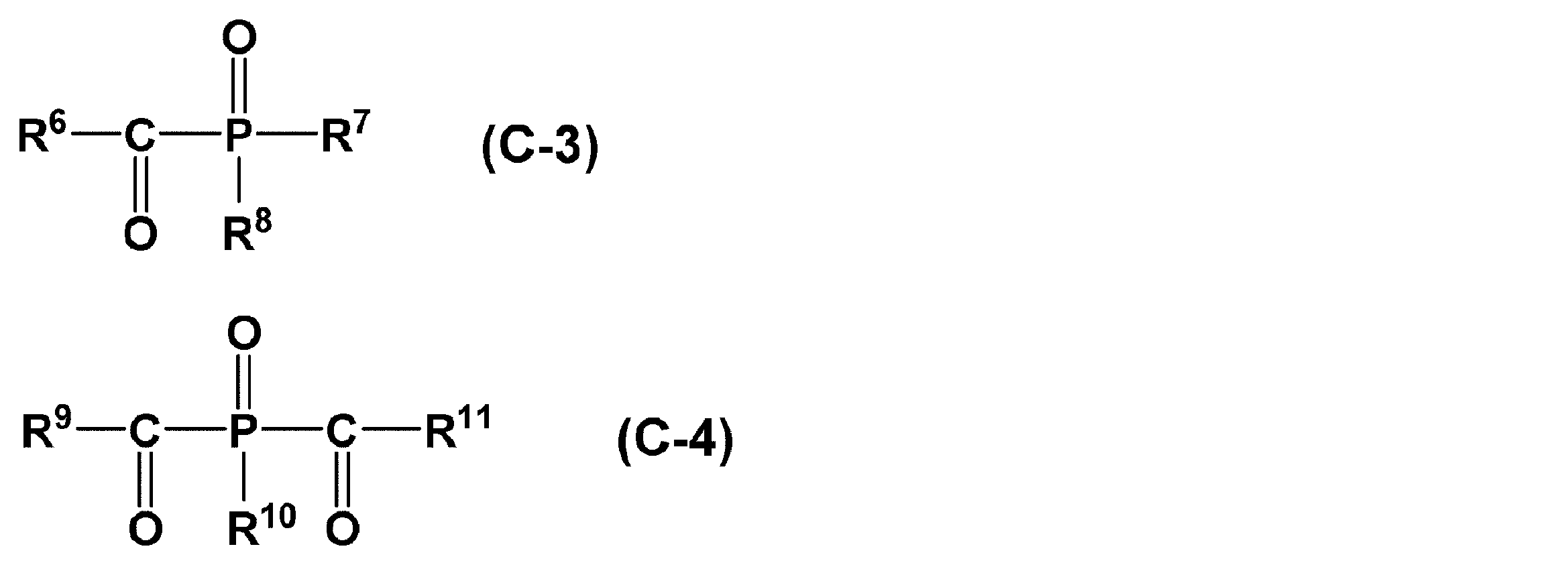
上記一般式(C-3)中、R6、R7及びR8はそれぞれ独立に、炭素数1~20のアルキル基又はアリール基を示す。一般式(C-4)中、R9、R10及びR11はそれぞれ独立に、炭素数1~20のアルキル基又はアリール基を示す。
上記一般式(C-3)におけるR6、R7又はR8が炭素数1~20のアルキル基の場合、及び、上記一般式(C-4)におけるR9、R10又はR11が、炭素数1~20のアルキル基の場合、該アルキル基は直鎖状、分岐鎖状、及び環状のいずれであってもよく、また該アルキル基の炭素数は5~10であることがより好ましい。
上記一般式(C-3)におけるR6、R7又はR8がアリール基の場合、及び、上記一般式(C-4)におけるR9、R10又はR11がアリール基の場合、該アリール基は置換基を有していてもよい。該置換基としては、例えば、炭素数1~6のアルキル基及び炭素数1~4のアルコキシ基を挙げることができる。
これらの中でも、上記一般式(C-3)は、R6、R7、及びR8がアリール基であることが好ましい。また、上記一般式(C-4)は、R9、R10及びR11が、アリール基であることが好ましい。
上記一般式(C-3)で表わされる化合物としては、形成される導電パターンの透明性、及び膜厚を薄く(例えば、10μm以下)したときのパターン形成能から、2,4,6-トリメチルベンゾイル-ジフェニル-ホスフィンオキサイドが好ましい。2,4,6-トリメチルベンゾイル-ジフェニル-ホスフィンオキサイドは、例えば、LUCIRIN TPO(BASF(株)社製、商品名)として商業的に入手可能である。
上記一般式(C-4)で表わされる化合物としては、形成される導電パターンの透明性、及び膜厚を薄く(例えば、10μm以下)したときのパターン形成能から、ビス(2,4,6-トリメチルベンゾイル)-フェニル-ホスフィンオキサイドが好ましい。ビス(2,4,6-トリメチルベンゾイル)-フェニル-ホスフィンオキサイドは、例えば、Irgacure 819(BASF(株)社製、商品名)として商業的に入手可能である。
オキシムエステル化合物、及びホスフィンオキサイド化合物以外で、透明性、及び感光層を薄膜化した場合のパターン形成能が良好である化合物としては、2,2-ジメトキシ-1,2-ジフェニルエタン-1-オンが好ましい。2,2-ジメトキシ-1,2-ジフェニルエタン-1-オンは、例えば、Irgacure 651(BASF(株)社製、商品名)として商業的に入手可能である。
(C)光重合開始剤は、1,2-オクタンジオン-1-[4-(フェニルチオ)フェニル]-2-(O-ベンゾイルオキシム)、エタノン,1-[9-エチル-6-(2-メチルベンゾイル)-9H-カルバゾール-3-イル]-,1-(O-アセチルオキシム)、2,4,6-トリメチルベンゾイル-ジフェニル-ホスフィンオキサイド、ビス(2,4,6-トリメチルベンゾイル)-フェニル-ホスフィンオキサイド、又は2,2-ジメトキシ-1,2-ジフェニルエタン-1-オンのいずれかを用いることが特に好ましい。
光重合開始剤の含有割合は、バインダーポリマー及び光重合性化合物の合計100質量部に対して、0.1~20質量部であることが好ましく、1~10質量部であることがより好ましく、1~5質量部であることがさらに好ましい。光感度に優れる点では、0.1質量部以上であることが好ましく、光硬化性に優れる点では、20質量部以下であることが好ましい。
(D)紫外線吸収剤について説明する。(D)紫外線吸収剤は、導電性繊維による散乱光吸収の観点から、波長400nm以下の紫外線の吸収能に優れ、かつ、透明性を向上させる観点から、波長400nm以上の可視光の吸収が少ないものが好ましい。具体的には、250nm以上400nm以下の波長域に極大吸収波長を有する材料がこれに該当する。
(D)紫外線吸収剤を感光層中に含有させることで、導電性繊維による散乱光を吸収し、ハレーションを抑制することができ、解像度の低下を充分に抑制することができる。また、紫外光によって導電膜及び導電パターン中に含まれる成分が分解して酸(例えば、酢酸等)が発生し、導電性繊維を腐食したり、劣化させたりすることで、導電パターンの抵抗が上昇する場合があるが、紫外線吸収剤を感光層中に含有させることで、抵抗の上昇を抑制することができる。
(D)紫外線吸収剤としては、オキシベンゾフェノン化合物、トリアゾール化合物,ベンゾトリアゾール化合物、サリチル酸エステル化合物、ベンゾフェノン化合物、ジフェニルアクリレート化合物、シアノアクリレート化合物、ジフェニルシアノアクリレート化合物、ニッケル錯塩化合物等が挙げられる。これらの中でも、ジフェニルシアノアクリレート化合物、シアノアクリレート化合物、又はジフェニルアクリレート化合物が好ましい。
(D)紫外線吸収剤は、反応性基を有する化合物であることが好ましく、熱重合性基又は光重合性基を有する化合物であることがより好ましい。紫外線吸収剤の含有量を増加させることにより、上記本発明の効果の向上を期待することができるが、紫外線吸収剤の含有量が増加した場合、パターニング後に樹脂硬化物から紫外線吸収剤が染み出す(ブリードアウトする)可能性がある。紫外線吸収剤のブリードアウトは、樹脂硬化物の透明性の低下、濁り等の光学特性の悪化などを引き起こす可能性があるため好ましくない。また、紫外線吸収剤の含有量が増加した場合、樹脂硬化物中にとり込まれていない紫外線吸収剤は、導電性繊維の表面に吸着する可能性がある。紫外線吸収剤の導電性繊維への吸着は、導電膜の抵抗値が上昇する原因となるため好ましくない。これらに対し、紫外線吸収剤が反応性基を有する場合には、パターニング中に、紫外線吸収剤が樹脂硬化物に固定される(例えば、樹脂硬化物のネットワーク内に共有結合で強固につながり、取り込まれる)ため、紫外線吸収剤の染み出し(ブリードアウト)又は樹脂硬化物中での紫外線吸収剤の移動が抑制される。そのため、紫外線吸収剤の含有量を増やしても、紫外線吸収剤の導電性繊維表面への吸着による抵抗値上昇を抑制することができる。
熱重合性基としては、エポキシ基、グリシジル基、イソシアネート基、アセチレン基、マレイミド基、オキセタニル基等が挙げられる。光重合性基としては、(メタ)アクリロイル基、アリル基、マレイミド基等が挙げられる。熱重合性基と光重合性基とは上記の例に限定されるものではない。本実施形態においては、熱又は光をきっかけとして発生する、活性ラジカル、酸、塩基によって、重合可能な反応性基を有する紫外線吸収剤であれば、特に制限なく用いることができ、紫外線吸収剤の染み出し(ブリードアウト)又は導電性繊維の表面への吸着を抑制することができる。
熱重合性基又は光重合性基を有する化合物のなかでも、入手のしやすさ、硬化前の感光性導電フィルム中の安定性の点から、光重合性基である(メタ)アクリロイル基を有する化合物が特に好ましい。このような紫外線吸収剤としては、(メタ)アクリロイル基を有するベンゾトリアゾール化合物である、2-[2-ヒドロキシ-5-[2-(メタクリロイルオキシ)エチル]フェニル]-2H-ベンゾトリアゾールが挙げられる。2-[2-ヒドロキシ-5-[2-(メタクリロイルオキシ)エチル]フェニル]-2H-ベンゾトリアゾールは、例えば、RUVA-93(大塚化学(株)製、商品名)やDAINSORB T-31(大和化成(株)製、商品名)として商業的に入手可能である。
(D)紫外線吸収剤は、ポリマー型紫外線吸収剤であることが好ましい。ポリマー型紫外線吸収剤とは、上述した熱反応性基又は光重合性基を有する化合物を重合して得られる紫外線吸収剤である。ポリマー型紫外線吸収剤は、分子内に1個以上の紫外線吸収部位を有する材料であり、かつ分子量が大きい材料である。「ポリマー型」であるための分子量について明確な境界は無いが、本明細書においては、重量平均分子量3000以上の紫外線吸収剤をポリマー型紫外線吸収剤という。ポリマー型紫外線吸収剤は、低分子の紫外線吸収剤に比べて、ブリードアウトが抑制されたものとなる。また、ポリマー型紫外線吸収剤は、導電性繊維表面への吸着が抑制されにくい。これにより、感光性導電フィルム中に多くの紫外線吸収剤を含有させることが可能になり、より効果的に導電性繊維による散乱光の影響を低減することができる。
ポリマー型紫外線吸収剤としては、原料である重合可能な反応性基を有する化合物の入手のし易さ、分子量の調整のし易さ、ポリマーの共重合成分を広く選択できる点から、光重合性基である(メタ)アクリロイル基を有する化合物を原料として、重合したポリマーが好ましい。
ポリマー型紫外線吸収剤としては、溶剤系RSAシリーズ(例えば、RSA-0124、RSA-0151、及びRSA-0191H;いずれも山南合成化学(株)製)、溶剤系PUVAシリーズ(例えば、PUVA-30M-50BA、PUVA-30M-30T、及びPUVA-50M-50K;いずれも大和化成(株)製)、溶剤系RSUシリーズ(例えば、RSU-0017、及びSG-864;いずれも大和化成(株)製)、水系RWUシリーズ(例えば、MW-022、RWU-0001、及びRWU-0109;いずれも大和化成(株)製)が商業的に入手可能である。また、水系ニューコートUVAシリーズ(例えば、ニューコートUVA-101、ニューコートUVA-102、ニューコートUVA-103、及びニューコートUVA-104)、溶剤系バナレジンUVAシリーズ(例えば、バナレジンUVA-5080、水酸基導入型バナレジンUVA-5080(OHV20)、バナレジンUVA-55T、高水酸基価タイプバナレジンUVA-55MHB、バナレジンUVA-7075、水酸基導入型バナレジンUVA-7075(OHV20)、及びバナレジンUVA-73T)等が新中村化学工業(株)から商業的に入手可能である。また、溶剤系UVAシリーズ(例えば、UVA-935LH、及びUVA-1935LH)、水系UVAシリーズ(例えば、UVA-700、及びUVA-1700)がBASF(株)から商業的に入手可能である。
ポリマー型紫外線吸収剤の重量平均分子量は、溶媒への溶解性、感光性樹脂組成物との相溶性の観点から、300000以下であることが好ましく、150000以下であることがより好ましく、100000以下であることがさらに好ましい。また、感光性導電フィルム及びその硬化膜からのブリードアウトを防ぐという観点から、3000以上であることが好ましく、5000以上であることがより好ましく、10000以上であることがさらに好ましい。溶媒への溶解性、感光性樹脂組成物との相溶性、及びブリードアウト防止性のバランスを図る観点から、3000~300000であることが好ましく、5000~150000であることがより好ましく、10000~100000であることがさらに好ましい。なお、重量平均分子量は、ゲルパーミエーションクロマトグラフィー法(GPC)により測定され、標準ポリスチレンを用いて作成した検量線により換算された値である。
(D)紫外線吸収剤の含有割合は、(A)成分及び(B)成分の合計量100質量部に対して、0.1~30質量部であることが好ましく、1~20質量部であることがより好ましく、2~10質量部であることがさらに好ましい。
(D)紫外線吸収剤の含有量は、導電性繊維による光散乱を効果的に抑制し、解像度に優れる点において、0.1質量部以上であることが好ましい。また、紫外線吸収剤の感光性導電フィルム及びその硬化膜からのブリードアウトを防止する点、導電性繊維の表面への吸着を抑制する点、又は活性光線照射の際に感光層の表面での吸収が増大して内部の光硬化が不充分となることを抑える点においては、30質量部以下であることが好ましい。
(D)紫外線吸収剤を感光層に含有させる方法としては、感光性樹脂組成物中にあらかじめ内部添加する方法が一般的であるが、本発明は内部添加に限るものではない。感光層中に紫外線吸収剤を含有させる他の方法としては、例えば、導電性繊維分散液中に紫外線吸収剤を内部添加する方法、支持フィルム上に形成した導電性繊維を含む膜を、紫外線吸収剤を含む液体にさらしたのち、改めて乾燥して導電膜を形成する方法等がある。感光性樹脂組成物中に均一に充分な量の紫外線吸収剤を含有させて、紫外線による導電性繊維の劣化又は断線を効果的に抑制するためには、感光性樹脂組成物中にあらかじめ内部添加する方法が、最も好ましい。
本実施形態の感光性樹脂組成物には、必要に応じて、シランカップリング剤等の密着性付与剤、レベリング剤、可塑剤、充填剤、消泡剤、難燃剤、安定剤、酸化防止剤、香料、熱架橋剤、重合禁止剤などを(A)成分及び(B)成分の合計量100質量部に対し、各々0.01~20質量部程度含有させることができる。
感光性樹脂層3は、メタノール、エタノール、アセトン、メチルエチルケトン、メチルセロソルブ、エチルセロソルブ、トルエン、N,N-ジメチルホルムアミド、プロピレングリコールモノメチルエーテル等の溶剤又はこれらの混合溶剤に溶解した感光性樹脂組成物の溶液を、導電膜2を形成した支持フィルム1上に、塗布、乾燥することにより形成できる。ただし、この場合、乾燥後の感光性樹脂層中の残存有機溶剤量は、後の工程での有機溶剤の拡散を防止するため、2質量%以下であることが好ましい。
感光性樹脂層3の塗工は、例えば、ロールコート法、コンマコート法、グラビアコート法、エアーナイフコート法、ダイコート法、バーコート法、スプレーコート法等の公知の方法で行うことができる。塗工後、有機溶剤等を除去するための乾燥は、70~150℃で5~30分間程度、熱風対流式乾燥機等で行うことができる。
感光性樹脂層3の厚みは、用途により異なるが、乾燥後の厚みで1~50μmであることが好ましく、1~15μmであることがより好ましく、1~10μmであることがさらに好ましい。この厚みが1μm未満では塗工が困難となる傾向があり、50μmを超えると光透過の低下による感度が不充分となり転写する感光性樹脂層の光硬化性が低下する傾向がある。感光性樹脂層3を硬化した後の層(硬化膜)の厚みについても、これらの範囲であることが好ましい。
本実施形態で用いる感光性導電フィルムにおいて、上記導電膜2及び上記感光性樹脂層3の積層体は、両層の合計膜厚を1~10μmとしたときに400nm以上700nm以下の波長域における可視光透過率の最小値が85%以上であることが好ましく、90%以上であることがより好ましい。導電膜及び感光性樹脂層がこのような条件を満たす場合、ディスプレイパネル等での視認性がより向上する。
本実施形態で用いる感光性導電フィルムは、透明電極として有効に活用する観点から、導電膜又は導電パターンの表面抵抗率が1000Ω/□以下であることが好ましく、500Ω/□以下であることがより好ましく、300Ω/□以下であることがさらに好ましい。表面抵抗率は、例えば、導電性繊維又は有機導電体の分散液の濃度又は塗工量によって調整することができる。
本実施形態で用いる感光性導電フィルムにおいて、感光性樹脂層3の支持フィルム1側とは反対側の面に接するように保護フィルム5を積層してもよい。
保護フィルム5としては、ポリエチレンテレフタレートフィルム、ポリプロピレンフィルム、ポリエチレンフィルム等の耐熱性及び耐溶剤性を有する重合体フィルムを用いることができる。また、保護フィルム5として上述の支持体フィルムと同様の重合体フィルムを用いてもよい。
保護フィルム5と感光層4との間の接着力は、保護フィルムを剥離し感光性樹脂層3側から基材にラミネートする場合は、保護フィルムを感光層から剥離しやすくするために、感光層4と支持フィルム1との間の接着力よりも小さいことが好ましい。
一方、保護フィルム5と感光層4との間の接着力は、支持フィルム1を剥離し導電膜2側から基材にラミネートする場合は、支持フィルムを感光層から剥離しやすくするために、感光層4と支持フィルム1との間の接着力よりも大きいことが好ましい。
一方、保護フィルム5と感光層4との間の接着力は、支持フィルム1を剥離し導電膜2側から基材にラミネートする場合は、支持フィルムを感光層から剥離しやすくするために、感光層4と支持フィルム1との間の接着力よりも大きいことが好ましい。
保護フィルム5は、保護フィルム中に含まれる直径80μm以上のフィッシュアイ数が5個/m2以下であることが好ましい。「フィッシュアイ」とは、材料を熱溶融し、混練、押し出し、2軸延伸、キャスティング法等によりフィルムを製造する際に、材料の異物、未溶解物、酸化劣化物等がフィルム中に取り込まれたものである。
保護フィルム5の厚みは、1~100μmであることが好ましく、5~50μmであることがより好ましく、5~30μmであることがさらに好ましく、15~30μmであることが特に好ましい。保護フィルムの厚みが1μm未満ではラミネートの際、保護フィルムが破れやすくなる傾向があり、100μmを超えると感光性導電フィルムの巻き取り性が低下する傾向がある。
<導電パターンの形成方法及び導電パターン付き基材>
本発明の導電パターンの形成方法は、本発明の感光性導電フィルムの感光層を基材上に転写する工程(ラミネート工程ともいう)と、基材上に転写された感光層にパターン状に活性光線を照射する露光工程と、感光層の未露光部を除去することにより導電パターンを形成する現像工程と、を備える。以下、本発明の導電パターンの形成方法を、図面を用いて説明する。
本発明の導電パターンの形成方法は、本発明の感光性導電フィルムの感光層を基材上に転写する工程(ラミネート工程ともいう)と、基材上に転写された感光層にパターン状に活性光線を照射する露光工程と、感光層の未露光部を除去することにより導電パターンを形成する現像工程と、を備える。以下、本発明の導電パターンの形成方法を、図面を用いて説明する。
図3は、感光性導電フィルムを用いた導電パターン形成方法の一実施形態を説明するための模式断面図である。本実施形態にかかる導電パターンの形成方法は、上述した感光性導電フィルム10を、支持フィルム1を剥離し、基材20上に導電層2が密着するようにラミネートするラミネート工程(図3(a))と、基材上の感光層4を露光及び現像することにより導電パターンを形成するパターンニング工程とを備える(図3(b)及び(c))。パターニング工程は、保護フィルム5を有する感光層4の所定部分に活性光線を照射する露光工程(図3(b))と、その後、保護フィルム5を剥離して感光層4を現像する現像工程(図3(c))とからなる。このようにして、導電パターン付き基材40が得られる。
図4は、感光性導電フィルムを用いた導電パターン形成方法の別の実施形態を説明するための模式断面図である。本実施形態にかかる導電パターンの形成方法と、上述した導電パターンの形成方法とは、感光層をラミネートする際に感光性樹脂層3が基材20上に密着するようにラミネートする点が異なる。すなわち、支持フィルム1、導電膜2及び感光性樹脂層3を有する感光性導電フィルム10を用意し、感光性導電フィルム10の感光性樹脂層3が基材20に密着するようにして、基材20上に感光層をラミネートする(図4の(a))。次に、感光性樹脂層3にマスクパターン6を介して活性光線Lをパターン状に照射し(図4の(b))、支持フィルム1を剥離した後、現像により未硬化部分(未露光部分)を除去することで導電パターン2aを形成する(図4の(c))。
上記導電パターンの形成方法は、本発明の感光性導電フィルムを、基材上に感光性樹脂層が密着するようにラミネートする工程と、上記支持フィルムを付けたまま基材上の感光性樹脂層の所定部分に活性光線を照射する露光工程と、その後上記支持フィルムを剥離する工程と、露光した感光性樹脂層を現像することにより導電パターンを形成する現像工程とを備える。これらの工程を経ることにより、基材上にパターニングされた導電パターンを備える導電パターン付き基材41が得られる。こうして得られる導電パターンは、導電パターン2aの厚みに加えて樹脂硬化パターン3bの厚みを有している。これらの厚みは基材との段差Hbとなり、この段差が大きいとディスプレイ等に要求される平滑性が得られにくくなる。また、段差が大きいと導電パターンが視認されやすくなる。そのため、用途によって図5に示す方法と使い分ければよい。
図5は、感光性導電フィルムを用いた導電パターンの形成方法の別の実施形態を説明するための模式断面図である。支持フィルム1を有する感光層4の所定部分に活性光線を照射する第一の露光工程(図5(b))後に、支持フィルム1を剥離してから、酸素存在下で、第一の露光工程での露光部及び未露光部の一部又は全部に活性光線を照射する第二の露光工程(図5(c))と、を備える。第二の露光工程は、酸素存在下、例えば、空気中で行うことが好ましい。また、酸素濃度を増やした条件でもよい。
図5の導電パターンの形成方法の現像工程では、第二の露光工程で露光した感光性樹脂層3の充分硬化していない表面部分が除去される。具体的には、ウェット現象により感光性樹脂層3の充分硬化していない表面部分、つまり導電膜2を含む表面層が除去される。これにより、基材20上に導電パターンとともに導電膜を有していない樹脂硬化層が設けられ、導電パターン付き基材42が得られ、基材上に導電パターンのみを設けた場合に比べて導電パターンの段差Haを小さくすることができる。
上記導電パターンの形成方法は、本発明の感光性導電フィルムを、基材上に感光性樹脂組成物が密着するようにラミネートする工程と、基材上に設けられた感光性樹脂層と、該感光性樹脂層の上記基材とは反対側の面に設けられた導電膜とを含む感光層に、パターン状に活性光線を照射する第一の露光工程と、酸素存在下で、上記感光層の少なくとも第一の露光工程での未露光部の一部又は全部に活性光線を照射する第二の露光工程と、上記第二の露光工程の後に上記感光層を現像することにより、導電パターンを形成する現像工程と、を備える。こうして得られる導電パターンは、樹脂硬化層3a上に形成される導電パターン2aは段差Haの小さくすることができる。
基材としては、ガラス基板、ポリカーボネート等のプラスチック基板等が挙げられる。基材は、400~700nmの波長域での最小光透過率が85%以上であるものが好ましい。
ラミネート工程は、例えば、感光性導電フィルムを、保護フィルム又は支持フィルムがある場合はそれを除去した後、加熱しながら感光性樹脂層又は導電膜側を基材に圧着することにより行われる。この作業は、密着性及び追従性の見地から減圧下で積層することが好ましい。感光性導電フィルムの積層は、感光層又は基材を70~130℃に加熱することが好ましく、圧着圧力は、0.1~1.0MPa程度(1~10kgf/cm2程度)とすることが好ましいが、これらの条件には特に制限はない。また、感光層を上記のように70~130℃に加熱すれば、予め基材を予熱処理することは必要ではないが、積層性をさらに向上させるために基材の予熱処理を行うこともできる。
支持フィルムを付けたまま基材上の感光層の所定部分に活性光線を照射する露光工程において、露光方法としては、アートワークと呼ばれるネガ又はポジマスクパターンを通して活性光線を画像状に照射する方法(マスク露光法)が挙げられる。活性光線の光源としては、公知の光源が用いられる。
露光工程での露光量は、用いる装置及び感光性樹脂組成物の組成によって異なるが、5mJ/cm2~1000mJ/cm2であることが好ましく、10mJ/cm2~200mJ/cm2であることがより好ましい。光硬化性に優れる点では、10mJ/cm2以上であることが好ましく、解像度の点では1000mJ/cm2以下であることが好ましい。露光工程は2段階に分けて行ってもよく、1段階目を上記の露光量で行ったあと、2段階目を100~10000mJ/cm2で行ってもよい。
ウェット現像は、アルカリ性水溶液、水系現像液、有機溶剤系現像液等、用いる感光性樹脂に対応した現像液を用いて、スプレー、揺動浸漬、ブラッシング、スクラッビング等の公知の方法により行われる。
現像液としては、アルカリ性水溶液等の安全かつ安定であり、操作性が良好なものが用いられる。上記アルカリ性水溶液の塩基としては、リチウム、ナトリウム又はカリウムの水酸化物等の水酸化アルカリ、リチウム、ナトリウム、カリウム又はアンモニウムの炭酸塩又は重炭酸塩等の炭酸アルカリ;リン酸カリウム、リン酸ナトリウム等のアルカリ金属リン酸塩;ピロリン酸ナトリウム、ピロリン酸カリウム等のアルカリ金属ピロリン酸塩などが用いられる。
現像に用いるアルカリ性水溶液としては、炭酸ナトリウム水溶液、炭酸カリウム水溶液、水酸化ナトリウム水溶液、四ホウ酸ナトリウム水溶液等が好ましい。上記アルカリ性水溶液の濃度は0.1~5質量%が通常用いられる。また、アルカリ性水溶液のpHは9~11の範囲とすることが好ましく、その温度は、感光性樹脂層の現像性に合わせて調節される。また、アルカリ性水溶液中には、表面活性剤、消泡剤、現像を促進させるための少量の有機溶剤等を混入させてもよい。
水又はアルカリ水溶液と、一種以上の有機溶剤とからなる水系現像液を用いることができる。ここで、アルカリ水溶液に含まれる塩基としては、上述の塩基以外に、ホウ砂、メタケイ酸ナトリウム、水酸化テトラメチルアンモニウム、エタノールアミン、エチレンジアミン、ジエチレントリアミン、2-アミノ-2-ヒドロキシメチル-1,3-プロパンジオール、1,3-ジアミノ-2-プロパノール、モルホリン等を用いてもよい。
有機溶剤としては、アセトン、酢酸エチル、炭素数1~4のアルコキシ基を有するアルコキシエタノール、エチルアルコール、イソプロピルアルコール、ブチルアルコール、ジエチレングリコールモノメチルエーテル、ジエチレングリコールモノエチルエーテル、ジエチレングリコールモノブチルエーテル等が挙げられる。
水系現像液は、有機溶剤の濃度を2~90質量%とすることが好ましく、その温度は、現像性にあわせて調整することができる。さらに、水系現像液のpHは、レジストの現像が充分にできる範囲でできるだけ小さくすることが好ましく、pH8~12とすることが好ましく、pH9~10とすることがより好ましい。また、水系現像液中には、界面活性剤、消泡剤等を少量添加することもできる。
有機溶剤系現像液としては、1,1,1-トリクロロエタン、N-メチルピロリドン、N,N-ジメチルホルムアミド、シクロヘキサノン、メチルイソブチルケトン、γ-ブチロラクトン等が挙げられる。これらの有機溶剤は、引火防止のため、1~20質量%の範囲で水を添加することが好ましい。
現像の方式としては、例えば、ディップ方式、パドル方式、高圧スプレー方式、ブラッシング、スラッピング等が挙げられる。これらのうち、高圧スプレー方式を用いることが、解像度向上の観点から好ましい。
本発明の導電パターンの形成方法においては、現像後に必要に応じて、60~250℃程度の加熱又は0.2~10J/cm2程度の露光を行うことにより導電パターンをさらに硬化してもよい。
本発明の導電パターンの形成方法によれば、ITO等の無機膜のようにエッチングレジストを形成することなく、ガラスやプラスチック等の基材上に容易に透明な導電パターンを形成することが可能である。
本発明の導電パターン付き基材は、上述した導電パターンの形成方法により得られるが、透明電極として有効に活用できる観点から、導電膜又は導電パターンの表面抵抗率が1000Ω/□以下であることが好ましく、500Ω/□以下であることがより好ましく、300Ω/□以下であることがさらに好ましい。表面抵抗率は、例えば、導電性繊維又は有機導電体の分散液の濃度又は塗工量によって調整することができる。
本発明の導電パターン付き基材は、400nm以上700nm以下の波長域における可視光透過率の最小値が80%以上であることが好ましく、85%以上であることがより好ましく、90%以上であることがさらに好ましい。導電パターン基板がこのような条件を満たす場合、ディスプレイパネル等における視認性がより向上する。光透過率は、導電性繊維又は有機導電体の分散液の濃度、塗工量によって調整することができる。また、導電性繊維の形状(繊維径、及び繊維長)によっても、透過率を調整することができる。繊維径が細いほど透過率は高くなる。
<タッチパネルセンサ>
本発明の導電パターンの形成方法、及び導電パターン付き基材は、それぞれ例えば、静電容量式タッチパネルの透明電極の形成、静電容量式タッチパネルセンサとして好ましく使用できる。
本発明の導電パターンの形成方法、及び導電パターン付き基材は、それぞれ例えば、静電容量式タッチパネルの透明電極の形成、静電容量式タッチパネルセンサとして好ましく使用できる。
図6は、静電容量式のタッチパネルセンサの一例を示す模式上面図である。図6は、タッチ画面102内に、透明基材101と透明電極(X位置座標)103及び透明電極(Y位置座標)104とを備える静電容量式タッチパネルセンサの一例を示す。透明電極103と透明電極104とは、同一平面上に存在してもよく、透明基材101上に積層されていてもよく、透明基材101を挟み込むように配置されていてもよい。
静電容量式タッチパネルは、上記の透明電極103及び104は、電気信号を制御するドライバ素子回路の制御回路に接続するための引き出し配線(図示せず)を有する。
本実施形態に係るタッチパネルセンサは、透明電極の少なくとも一方は、本発明の感光性導電フィルムを用いて形成される。この場合、他方の透明電極は、透明導電材料を用いた公知の方法で、透明基材上に予め形成してもよい。
以下に、本発明を実施例に基づいて具体的に説明するが、本発明はこれに限定されるものではない。
実施例、比較例で用いた成分は以下のとおりである。
(B)成分
・トリメチロールプロパントリアクリレート(日本化薬(株)製、商品名「TMPTA」)
(B)成分
・トリメチロールプロパントリアクリレート(日本化薬(株)製、商品名「TMPTA」)
(C)成分
・1,2-オクタンジオン,1-[4-(フェニルチオ)フェニル-,2-(O-ベンゾイルオキシム)](BASF(株)製、商品名「OXE-01」)
・2,4,6-トリメチルベンゾイル-ジフェニル-ホスフィンオキサイド(BASF(株)製、商品名「LUCIRIN TPO」)
・2,2-ジメトキシ-1,2-ジフェニルエタン-1-オン(BASF(株)製、商品名「Irgacure 651」)
・1,2-オクタンジオン,1-[4-(フェニルチオ)フェニル-,2-(O-ベンゾイルオキシム)](BASF(株)製、商品名「OXE-01」)
・2,4,6-トリメチルベンゾイル-ジフェニル-ホスフィンオキサイド(BASF(株)製、商品名「LUCIRIN TPO」)
・2,2-ジメトキシ-1,2-ジフェニルエタン-1-オン(BASF(株)製、商品名「Irgacure 651」)
(D)成分
・2-シアノ-3,3-ジフェニルアクリル酸エチル(シプロ化成(株)製、商品名「SEESORB501」)
・2-[2-ヒドロキシ-5-[2-(メタクリロイルオキシ)エチル]フェニル]-2H-ベンゾトリアゾール(大塚化学(株)製、商品名「RUVA-93」)
・ポリマー型紫外線吸収剤(大和化成(株)製、商品名「PUVA-50M-50K」)
・2-シアノ-3,3-ジフェニルアクリル酸エチル(シプロ化成(株)製、商品名「SEESORB501」)
・2-[2-ヒドロキシ-5-[2-(メタクリロイルオキシ)エチル]フェニル]-2H-ベンゾトリアゾール(大塚化学(株)製、商品名「RUVA-93」)
・ポリマー型紫外線吸収剤(大和化成(株)製、商品名「PUVA-50M-50K」)
・カーボンナノチューブ(Hipco単層カーボンナノチューブ高純度品、Unidym社製)
・ドデシルーペンタエチレングリコール(和光純薬(株)製)
・ドデシルーペンタエチレングリコール(和光純薬(株)製)
(その他の成分)
・オクタメチルシクロテトラシロキサン(東レ・ダウコーニング(株)製、商品名「SH-30」)(レベリング剤)
・メチルエチルケトン(東燃化学(株)製)(溶媒)
・オクタメチルシクロテトラシロキサン(東レ・ダウコーニング(株)製、商品名「SH-30」)(レベリング剤)
・メチルエチルケトン(東燃化学(株)製)(溶媒)
製造例1
<銀繊維分散液(導電性繊維分散液(導電膜形成用塗液))の調製>
[ポリオール法による銀繊維の調製]
2000mLの3口フラスコに、エチレングリコール500mLを入れ、窒素雰囲気下、マグネチックスターラーで攪拌しながらオイルバスを用いて160℃まで加熱した。ここに、別途用意した溶液1(2mgのPtCl2を50mLのエチレングリコールに溶解した溶液)を滴下した。4~5分後、溶液2(5gのAgNO3をエチレングリコール300mLに溶解した溶液)と、溶液3(ポリビニルピロリドン(和光純薬(株)製、重量平均分子量:58000)5gをエチレングリコール150mLに溶解した溶液)とを、それぞれの滴下漏斗から1分間で滴下し、反応溶液を160℃で60分間攪拌した。
<銀繊維分散液(導電性繊維分散液(導電膜形成用塗液))の調製>
[ポリオール法による銀繊維の調製]
2000mLの3口フラスコに、エチレングリコール500mLを入れ、窒素雰囲気下、マグネチックスターラーで攪拌しながらオイルバスを用いて160℃まで加熱した。ここに、別途用意した溶液1(2mgのPtCl2を50mLのエチレングリコールに溶解した溶液)を滴下した。4~5分後、溶液2(5gのAgNO3をエチレングリコール300mLに溶解した溶液)と、溶液3(ポリビニルピロリドン(和光純薬(株)製、重量平均分子量:58000)5gをエチレングリコール150mLに溶解した溶液)とを、それぞれの滴下漏斗から1分間で滴下し、反応溶液を160℃で60分間攪拌した。
上記反応溶液が30℃以下になるまで放置した後、アセトンで10倍に希釈した。上記反応溶液の希釈液を、遠心分離機により2000回転で20分間遠心分離し、上澄み液をデカンテーションした。沈殿物にアセトンを加え、攪拌後に、上記と同様の条件で遠心分離し、アセトンをデカンテーションした。その後、蒸留水を用いて同様に2回遠心分離して、銀繊維を得た。得られた銀繊維を光学顕微鏡で観察したところ、繊維径(直径)は30nmで、繊維長は3μmであった。
[銀繊維分散液の調製]
純水に、上記で得られた銀繊維が0.2質量%の濃度となるように、また、ドデシルーペンタエチレングリコールが0.1質量%の濃度となるように分散し、銀繊維分散液を得た。
純水に、上記で得られた銀繊維が0.2質量%の濃度となるように、また、ドデシルーペンタエチレングリコールが0.1質量%の濃度となるように分散し、銀繊維分散液を得た。
<カーボンナノチューブ分散液の調製>
純水に、Unidym社のHipco単層カーボンナノチューブの高純度品を0.4質量%、及び界面活性剤としてドデシルーペンタエチレングリコールを0.1質量%の濃度となるように分散し、カーボンナノチューブ分散液を得た。
純水に、Unidym社のHipco単層カーボンナノチューブの高純度品を0.4質量%、及び界面活性剤としてドデシルーペンタエチレングリコールを0.1質量%の濃度となるように分散し、カーボンナノチューブ分散液を得た。
製造例2
<バインダーポリマー(A1)溶液の調製>
撹拌機、還流冷却機、不活性ガス導入口及び温度計を備えたフラスコに、表1に示す(1)を仕込み、窒素ガス雰囲気下で80℃に昇温した。反応温度を80℃±2℃に保ちながら、表1に示す(2)を4時間かけて均一に滴下した。(2)の滴下後、80℃±2℃で6時間撹拌を続け、重量平均分子量が45000のバインダーポリマー(A1)溶液(固形分50質量%)を得た。バインダーポリマー(A1)の酸価は、78mgKOH/gであった。また、ガラス転移温度(Tg)は60℃であった。
<バインダーポリマー(A1)溶液の調製>
撹拌機、還流冷却機、不活性ガス導入口及び温度計を備えたフラスコに、表1に示す(1)を仕込み、窒素ガス雰囲気下で80℃に昇温した。反応温度を80℃±2℃に保ちながら、表1に示す(2)を4時間かけて均一に滴下した。(2)の滴下後、80℃±2℃で6時間撹拌を続け、重量平均分子量が45000のバインダーポリマー(A1)溶液(固形分50質量%)を得た。バインダーポリマー(A1)の酸価は、78mgKOH/gであった。また、ガラス転移温度(Tg)は60℃であった。

製造例3
<ポリマー型紫外線吸収剤(D1)溶液の調製>
撹拌機、還流冷却機、不活性ガス導入口及び温度計を備えたフラスコに、表2に示す(1)を仕込み、窒素ガス雰囲気下で80℃に昇温した。反応温度を80℃±2℃に保ちながら、表2に示す(2)を4時間かけて均一に滴下した。(2)の滴下後、80℃±2℃で6時間撹拌を続け、重量平均分子量が15000のポリマー型紫外線吸収剤(D1)溶液(固形分50質量%)を得た。ポリマー型紫外線吸収剤(D1)の酸価は、0mgKOH/gであった。
<ポリマー型紫外線吸収剤(D1)溶液の調製>
撹拌機、還流冷却機、不活性ガス導入口及び温度計を備えたフラスコに、表2に示す(1)を仕込み、窒素ガス雰囲気下で80℃に昇温した。反応温度を80℃±2℃に保ちながら、表2に示す(2)を4時間かけて均一に滴下した。(2)の滴下後、80℃±2℃で6時間撹拌を続け、重量平均分子量が15000のポリマー型紫外線吸収剤(D1)溶液(固形分50質量%)を得た。ポリマー型紫外線吸収剤(D1)の酸価は、0mgKOH/gであった。

作製したポリマー溶液の特性は、以下の方法で測定した。
(1)重量平均分子量
重量平均分子量(Mw)は、ゲルパーミエーションクロマトグラフィー法(GPC)によって測定し、標準ポリスチレンの検量線を用いて換算することにより導出した。GPCの条件を以下に示す。
重量平均分子量(Mw)は、ゲルパーミエーションクロマトグラフィー法(GPC)によって測定し、標準ポリスチレンの検量線を用いて換算することにより導出した。GPCの条件を以下に示す。
ポンプ:日立 L-6000型((株)日立製作所製、商品名)
カラム:Gelpack GL-R420、Gelpack GL-R430、Gelpack GL-R440(以上、日立化成(株)製、商品名)
溶離液:テトラヒドロフラン
測定温度:40℃
流量:2.05mL/分
検出器:日立 L-3300型RI((株)日立製作所製、商品名)
カラム:Gelpack GL-R420、Gelpack GL-R430、Gelpack GL-R440(以上、日立化成(株)製、商品名)
溶離液:テトラヒドロフラン
測定温度:40℃
流量:2.05mL/分
検出器:日立 L-3300型RI((株)日立製作所製、商品名)
(2)酸価
酸価は、次のようにして測定した。まず、バインダーポリマーの溶液を、130℃で1時間加熱し、揮発分を除去して、固形のポリマーを得た。そして、固形のポリマー1gを精秤した後、精秤したポリマーを三角フラスコに入れ、アセトンを30g添加し、均一に溶解した。次いで、指示薬であるフェノールフタレインをその溶液に適量添加して、0.1NのKOH水溶液を用いて滴定を行った。そして、次式により酸価を算出した。
酸価=0.1×Vf×56.1/(Wp×I/100)
式中、VfはKOH水溶液の滴定量(mL)を示し、Wpは測定した樹脂溶液の質量(g)を示し、Iは測定した樹脂溶液中の不揮発分の割合(質量%)を示す。なお、ポリマー型紫外線吸収剤(D1)の酸価も同様の操作により算出した。
酸価は、次のようにして測定した。まず、バインダーポリマーの溶液を、130℃で1時間加熱し、揮発分を除去して、固形のポリマーを得た。そして、固形のポリマー1gを精秤した後、精秤したポリマーを三角フラスコに入れ、アセトンを30g添加し、均一に溶解した。次いで、指示薬であるフェノールフタレインをその溶液に適量添加して、0.1NのKOH水溶液を用いて滴定を行った。そして、次式により酸価を算出した。
酸価=0.1×Vf×56.1/(Wp×I/100)
式中、VfはKOH水溶液の滴定量(mL)を示し、Wpは測定した樹脂溶液の質量(g)を示し、Iは測定した樹脂溶液中の不揮発分の割合(質量%)を示す。なお、ポリマー型紫外線吸収剤(D1)の酸価も同様の操作により算出した。
(3)ガラス転移温度(Tg)
上記作製したバインダーポリマーの溶液をポリエチレンテレフタレートフィルム(帝人デュポンフィルム(株)製、商品名「ピューレックスA53」)上に均一に塗布し、90℃の熱風対流式乾燥機で10分間乾燥して、乾燥後の厚さが40μmであるバインダーポリマーからなる膜を形成した。次いで高圧水銀灯を有する露光機((株)オーク製作所製、商品名「EXM-1201」)を用いて、照射エネルギー量が400mJ/cm2(i線(波長365nm)における測定値)となるように上記膜を露光した。露光された膜をホットプレート上にて65℃で2分間、次いで95℃で8分間加熱し、熱風対流式乾燥機にて180℃で60分間加熱処理をした後、ポリエチレンテレフタレートフィルムから剥離し、TMA/SS6000(セイコーインスツルメンツ社製)を用いて、昇温速度5℃/分で温度を上昇させたときの上記硬化膜の熱膨張率を測定し、その曲線から得られる変曲点をガラス転移温度Tgとして求めた。
上記作製したバインダーポリマーの溶液をポリエチレンテレフタレートフィルム(帝人デュポンフィルム(株)製、商品名「ピューレックスA53」)上に均一に塗布し、90℃の熱風対流式乾燥機で10分間乾燥して、乾燥後の厚さが40μmであるバインダーポリマーからなる膜を形成した。次いで高圧水銀灯を有する露光機((株)オーク製作所製、商品名「EXM-1201」)を用いて、照射エネルギー量が400mJ/cm2(i線(波長365nm)における測定値)となるように上記膜を露光した。露光された膜をホットプレート上にて65℃で2分間、次いで95℃で8分間加熱し、熱風対流式乾燥機にて180℃で60分間加熱処理をした後、ポリエチレンテレフタレートフィルムから剥離し、TMA/SS6000(セイコーインスツルメンツ社製)を用いて、昇温速度5℃/分で温度を上昇させたときの上記硬化膜の熱膨張率を測定し、その曲線から得られる変曲点をガラス転移温度Tgとして求めた。
実施例1
<感光性導電フィルムV1の作製>
[導電フィルム(感光性導電フィルムの導電膜)W1の作製]
上記製造例1で得られた銀繊維分散液を、50μm厚のポリエチレンテレフタレートフィルム(PETフィルム、帝人(株)製、商品名「G2-50」)上に25g/m2で均一に塗布し、100℃の熱風対流式乾燥機で3分間乾燥し、導電フィルムW1を形成した。導電膜の乾燥後の膜厚は、0.1μmであった。
<感光性導電フィルムV1の作製>
[導電フィルム(感光性導電フィルムの導電膜)W1の作製]
上記製造例1で得られた銀繊維分散液を、50μm厚のポリエチレンテレフタレートフィルム(PETフィルム、帝人(株)製、商品名「G2-50」)上に25g/m2で均一に塗布し、100℃の熱風対流式乾燥機で3分間乾燥し、導電フィルムW1を形成した。導電膜の乾燥後の膜厚は、0.1μmであった。
[感光性樹脂組成物の溶液X1の作製]
表3に示す材料を、表3に示す配合量(質量部)で、攪拌機を用いて15分間混合し、感光性樹脂組成物の溶液X1を作製した。(A)成分の配合量は固形分の質量である。
表3に示す材料を、表3に示す配合量(質量部)で、攪拌機を用いて15分間混合し、感光性樹脂組成物の溶液X1を作製した。(A)成分の配合量は固形分の質量である。

[感光性導電フィルムV1の作製]
感光性樹脂組成物の溶液X1を、上記導電フィルムW1上に均一に塗布し、100℃の熱風対流式乾燥機で10分間乾燥して感光性樹脂層を形成した。その後、感光性樹脂層を、ポリエチレンフィルム(タマポリ(株)製、商品名「NF-13」)で覆い、感光性導電フィルムV1を得た。感光性樹脂層の乾燥後の膜厚は5μmであった。
感光性樹脂組成物の溶液X1を、上記導電フィルムW1上に均一に塗布し、100℃の熱風対流式乾燥機で10分間乾燥して感光性樹脂層を形成した。その後、感光性樹脂層を、ポリエチレンフィルム(タマポリ(株)製、商品名「NF-13」)で覆い、感光性導電フィルムV1を得た。感光性樹脂層の乾燥後の膜厚は5μmであった。
<感光性導電フィルムV1の評価>
[感光性導電フィルムV1の光透過率の測定]
得られた感光性導電フィルムV1のポリエチレンフィルムを剥がしながら、厚さ1mmのガラス基板上に、感光性樹脂層が接するようにラミネータ(日立化成株式会社製、商品名「HLM-3000型」)を用いて、ロール温度110℃、基板送り速度1m/分、圧着圧力(シリンダ圧力)4×105Pa(厚さが1mm、縦10cm×横10cmの基板を用いたため、この時の線圧は9.8×103N/m)の条件でラミネートして、ガラス基板上に、支持フィルムを含む感光性導電フィルムV1が積層された基板を作製した。
[感光性導電フィルムV1の光透過率の測定]
得られた感光性導電フィルムV1のポリエチレンフィルムを剥がしながら、厚さ1mmのガラス基板上に、感光性樹脂層が接するようにラミネータ(日立化成株式会社製、商品名「HLM-3000型」)を用いて、ロール温度110℃、基板送り速度1m/分、圧着圧力(シリンダ圧力)4×105Pa(厚さが1mm、縦10cm×横10cmの基板を用いたため、この時の線圧は9.8×103N/m)の条件でラミネートして、ガラス基板上に、支持フィルムを含む感光性導電フィルムV1が積層された基板を作製した。
次いで、ガラス基板上の感光性導電フィルムに、平行光線露光機(オーク製作所(株)製、EXM1201)を使用して、支持フィルム側より露光量5×10²J/m2(i線(波長365nm)における測定値)で、紫外線を照射した。その後、支持フィルムを除去し、さらに平行光線露光機で導電膜側から、露光量1×104J/m2(i線(波長365nm)における測定値)で紫外線を照射し、感光性樹脂層と導電膜(感光層)(膜厚5.0μm)の透過率測定用試料を得た。
次いで、得られた試料を紫外可視分光光度計(日立計測器サービス(株)製、商品名「U-3310」)を使用して、測定波長域300~380nmで紫外光透過率を、測定波長域400~700nmで可視光透過率を測定した。なお、ガラス基板をバックグラウンドとし、感光性導電フィルム単独での透過率を測定した。
得られた感光性導電フィルムの可視光透過率は、波長700nmにおいて99%、波長550nmにおいて99%、波長400nmにおいて87%であった。400nm以上700nm以下の波長域における可視光透過率の最小値は87%であり、良好な透過率を確保できていた。また、紫外光透過率は、380nmにおいて71%であり、300nmにおいて15%であった。300~380nmの紫外光透過率の最大値は71%であった。
[感光性導電フィルムV1の表面抵抗率の測定]
感光性導電フィルムV1の光透過率の測定方法と同様にして、ガラス基板上に感光性導電フィルムV1を積層した、表面抵抗率測定用のサンプルを作製した。サンプルの表面抵抗率を非接触抵抗測定器(ナプソン(株)製、商品名「EC-80P」)によって測定したところ、100±5Ω/□であった。
感光性導電フィルムV1の光透過率の測定方法と同様にして、ガラス基板上に感光性導電フィルムV1を積層した、表面抵抗率測定用のサンプルを作製した。サンプルの表面抵抗率を非接触抵抗測定器(ナプソン(株)製、商品名「EC-80P」)によって測定したところ、100±5Ω/□であった。
[感光性導電フィルムV1の感度の測定]
PETフィルム基板(厚さ50μm、東洋紡績製、商品名「A4100」)の易接着面に、感光性導電フィルムV1のポリエチレンフィルムを剥がしながら、感光性樹脂層が接するようにラミネータ(日立化成株式会社製、商品名「HLM-3000型」)を用いて、ロール温度110℃、基板送り速度1m/分、圧着圧力(シリンダ圧力)4×105Paの条件でラミネートして、PETフィルム基板上に、支持フィルムを含む感光性導電フィルムV1が積層されたフィルム基板を作製した。
PETフィルム基板(厚さ50μm、東洋紡績製、商品名「A4100」)の易接着面に、感光性導電フィルムV1のポリエチレンフィルムを剥がしながら、感光性樹脂層が接するようにラミネータ(日立化成株式会社製、商品名「HLM-3000型」)を用いて、ロール温度110℃、基板送り速度1m/分、圧着圧力(シリンダ圧力)4×105Paの条件でラミネートして、PETフィルム基板上に、支持フィルムを含む感光性導電フィルムV1が積層されたフィルム基板を作製した。
次いで、フィルム基板上の感光性導電フィルムの支持フィルム1に、41段ステップタブレット(日立化成株式会社製)をフォトマスクとして密着させ、平行光線露光機(オーク製作所(株)製、商品名「EXM1201」)を使用して、支持フィルム1側よりフォトマスクを介して露光した。露光量は、4×10²J/m2(i線(波長365nm)における測定値)とした。露光後、室温(23℃~25℃)で15分間放置した後、支持フィルム1を除去し、続いて、30℃で1質量%炭酸ナトリウム水溶液を30秒間スプレーすることにより現像した。現像により感光性導電フィルムの導電パターンが樹脂硬化パターン上に形成した。そして、現像後の残存ステップ段数により感度を評価した。感光性導電フィルムV1の感度を評価したところ、8段であった。残存しているステップタブレットの段数が高いほど(数値が大きいほど)高感度であることを意味する。
[感光性導電フィルムV1の解像度の測定(フル現像プロセス)]
PETフィルム基板(厚さ50μm、東洋紡績製、商品名「A4100」)の易接着面に、感光性導電フィルムV1のポリエチレンフィルムを剥がしながら、感光性樹脂層が接するようにラミネータ(日立化成株式会社製、商品名「HLM-3000型」)を用いて、ロール温度110℃、基板送り速度1m/分、圧着圧力(シリンダ圧力)4×105Paの条件でラミネートして、PETフィルム基板上に、支持フィルムを含む感光性導電フィルムV1が積層されたフィルム基板を作製した。
PETフィルム基板(厚さ50μm、東洋紡績製、商品名「A4100」)の易接着面に、感光性導電フィルムV1のポリエチレンフィルムを剥がしながら、感光性樹脂層が接するようにラミネータ(日立化成株式会社製、商品名「HLM-3000型」)を用いて、ロール温度110℃、基板送り速度1m/分、圧着圧力(シリンダ圧力)4×105Paの条件でラミネートして、PETフィルム基板上に、支持フィルムを含む感光性導電フィルムV1が積層されたフィルム基板を作製した。
次いで、フィルム基板上の感光性導電フィルムの支持フィルム1に、ライン幅/スペース幅が6/6~47/47(単位:μm)の配線パターンを有するPET製のフォトマスクを密着させ、平行光線露光機(オーク製作所(株)製、商品名「EXM1201」)を使用して、支持フィルム1側よりフォトマスクを介して露光した。露光量は、41段ステップタブレット(日立化成株式会社製)における感度が、8段となる露光量とした。露光後、室温(23℃~25℃)で15分間放置した後、支持フィルム1を除去し、続いて、30℃で1質量%炭酸ナトリウム水溶液を30秒間スプレーすることにより現像した。現像後の導電パターンを光学顕微鏡で観察することで、現像処理によって未露光部の導電層をきれいに除去することができ、かつ露光部が欠けなく導電パターンを形成できた。ライン幅/スペース幅の最も小さい値により解像度を評価した。感光性導電フィルムV1の解像度を評価したところ、25μmであった。解像度の評価は、数値が小さいほど良好であることを意味する。
[感光性導電フィルムV1の解像度の測定(低段差現像プロセス)]
PETフィルム基板(厚さ50μm、東洋紡績製、商品名「A4100」)の易接着面に,感光性導電フィルムV1のポリエチレンフィルムを剥がしながら、感光性樹脂層が接するようにラミネータ(日立化成株式会社製、商品名「HLM-3000型」)を用いて、ロール温度110℃、基板送り速度1m/分、圧着圧力(シリンダ圧力)4×105Paの条件でラミネートして、PETフィルム基板上に、支持フィルムを含む感光性導電フィルムV1が積層されたフィルム基板を作製した。
PETフィルム基板(厚さ50μm、東洋紡績製、商品名「A4100」)の易接着面に,感光性導電フィルムV1のポリエチレンフィルムを剥がしながら、感光性樹脂層が接するようにラミネータ(日立化成株式会社製、商品名「HLM-3000型」)を用いて、ロール温度110℃、基板送り速度1m/分、圧着圧力(シリンダ圧力)4×105Paの条件でラミネートして、PETフィルム基板上に、支持フィルムを含む感光性導電フィルムV1が積層されたフィルム基板を作製した。
次いで、フィルム基板上の感光性導電フィルムの支持フィルム1に、ライン幅/スペース幅が6/6~47/47(単位:μm)の配線パターンを有するPET製のフォトマスクを密着させ、平行光線露光機(オーク製作所(株)製、商品名「EXM1201」)を使用して、支持フィルム1側よりフォトマスクを介して露光した(1段目露光)。露光量は、41段ステップタブレット(日立化成株式会社製)における感度が、8段となる露光量とした。次に、フォトマスクと支持フィルム1を除去し、さらに感光性導電フィルムの導電層上方より、大気中環境で(酸素存在下で)フィルム全面に露光した(2段目露光)。露光量は、先程の1段目露光の3倍の露光量とした。
露光後、室温(23℃~25℃)で15分間放置した後、30℃で1質量%炭酸ナトリウム水溶液を30秒間スプレーすることにより現像した。現像後の導電パターンを光学顕微鏡で観察することで、現像処理によって1段目露光時に未露光部であった部分で、導電層の導電性繊維がきれいに除去することができ、かつ1段目露光時に露光部であった部分で、欠けなく導電性繊維のパターンを形成できた、ライン幅/スペース幅の最も小さい値により解像度を評価した。感光性導電フィルムV1の解像度を評価したところ、20μmであった。解像度の評価は、数値が小さいほど良好であることを意味する。
実施例2~6
表4に示す感光性樹脂組成物の溶液(X)を用いた以外は、実施例1と同様に感光性導電フィルムを作製し、各種特性を評価した。結果を表4に示す。
表4に示す感光性樹脂組成物の溶液(X)を用いた以外は、実施例1と同様に感光性導電フィルムを作製し、各種特性を評価した。結果を表4に示す。
実施例7,8
導電フィルムW1の代わりに導電フィルムW2又はW3を用いたこと以外は、実施例1と同様に感光性導電フィルムを作製し、各種特性を評価した。結果を表4に示す。導電フィルムW2及びW3の作製方法は以下のとおりである。
導電フィルムW1の代わりに導電フィルムW2又はW3を用いたこと以外は、実施例1と同様に感光性導電フィルムを作製し、各種特性を評価した。結果を表4に示す。導電フィルムW2及びW3の作製方法は以下のとおりである。
[導電フィルム(感光性導電フィルムの導電膜)W2の作製]
上記製造例1で得られた銀繊維分散液を、50μm厚のポリエチレンテレフタレートフィルム(PETフィルム、帝人(株)製、商品名「G2-50」)上に20g/m2で均一に塗布し、100℃の熱風対流式乾燥機で3分間乾燥し、導電フィルムW2を形成した。導電膜の乾燥後の膜厚は、0.08μmであった。
上記製造例1で得られた銀繊維分散液を、50μm厚のポリエチレンテレフタレートフィルム(PETフィルム、帝人(株)製、商品名「G2-50」)上に20g/m2で均一に塗布し、100℃の熱風対流式乾燥機で3分間乾燥し、導電フィルムW2を形成した。導電膜の乾燥後の膜厚は、0.08μmであった。
[導電フィルム(感光性導電フィルムの導電膜)W3の作製]
上記製造例1で得られたカーボンナノチューブ分散液を、50μm厚のポリエチレンテレフタレートフィルム(PETフィルム、帝人(株)製、商品名「G2-50」)上に30g/m2で均一に塗布し、100℃の熱風対流式乾燥機で3分間乾燥し、導電フィルムW3を形成した。導電膜の乾燥後の膜厚は、0.05μmであった。
上記製造例1で得られたカーボンナノチューブ分散液を、50μm厚のポリエチレンテレフタレートフィルム(PETフィルム、帝人(株)製、商品名「G2-50」)上に30g/m2で均一に塗布し、100℃の熱風対流式乾燥機で3分間乾燥し、導電フィルムW3を形成した。導電膜の乾燥後の膜厚は、0.05μmであった。
比較例1~3
表5に示す感光性樹脂組成物の溶液(X)を用いた以外は、実施例1と同様に感光性導電フィルムを作製し、各種特性を評価した。結果を表5に示す。
表5に示す感光性樹脂組成物の溶液(X)を用いた以外は、実施例1と同様に感光性導電フィルムを作製し、各種特性を評価した。結果を表5に示す。
比較例4
導電フィルムW1の代わりに導電フィルムW3を用いたこと、そして表5に示す感光性樹脂組成物の溶液(X)を用いた以外は、実施例1と同様に感光性導電フィルムを作製し、各種特性を評価した。結果を表5に示す。
導電フィルムW1の代わりに導電フィルムW3を用いたこと、そして表5に示す感光性樹脂組成物の溶液(X)を用いた以外は、実施例1と同様に感光性導電フィルムを作製し、各種特性を評価した。結果を表5に示す。
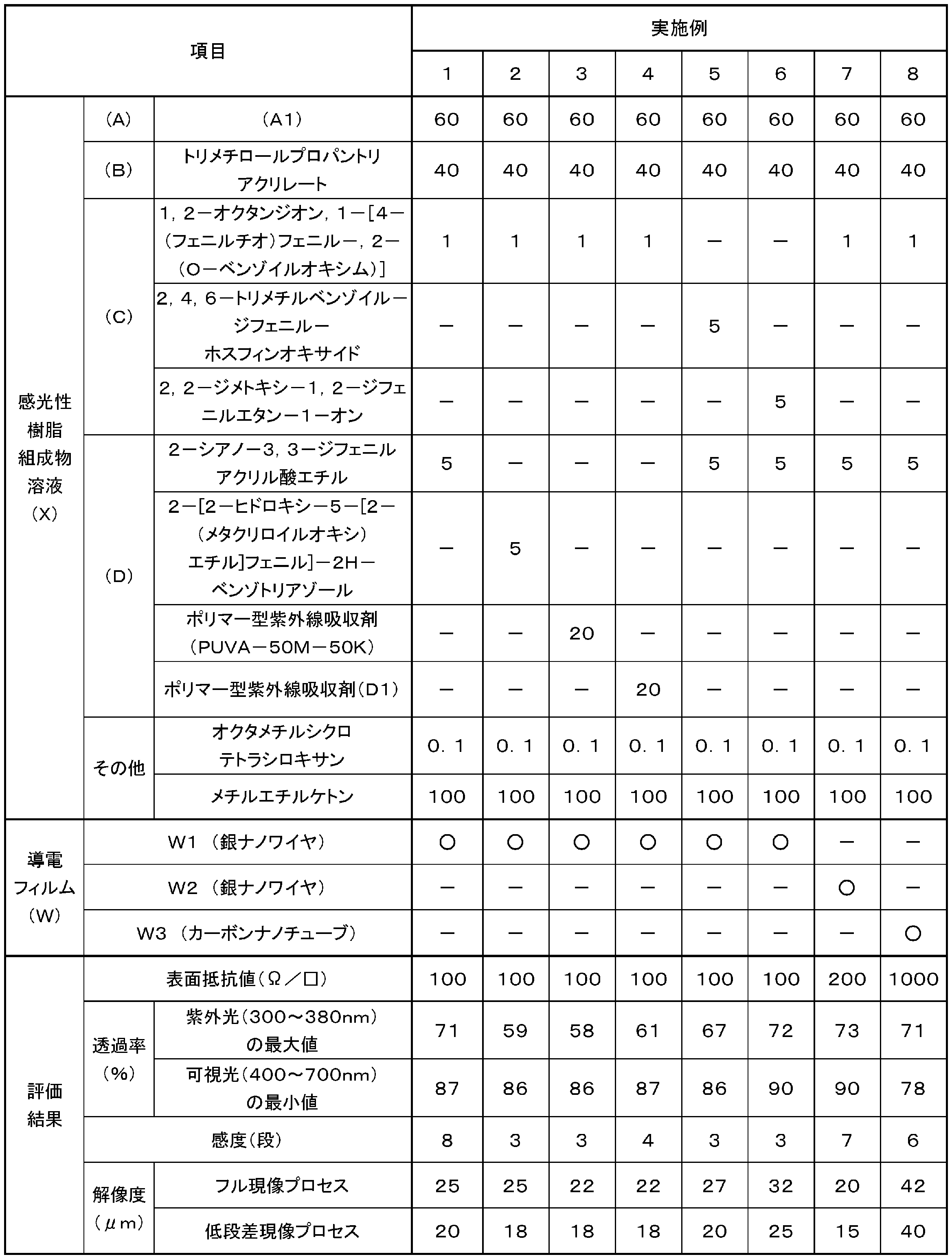

表4及び表5に示されるように、(D)成分である紫外線吸収剤を含む感光層を用いることで解像度が向上していることが確認された。より具体的には、感光層が銀ナノワイヤを含む実施例1~7は、比較例1~3に比べて優れた解像度を示し、感光層がカーボンナノチューブを含む実施例8は、比較例4に比べて優れた解像度を示すことが確認された。
本発明の感光性導電フィルムを用いれば、感光層が導電性繊維を含む場合であっても、充分な解像度で導電パターンを形成することができる。また、充分な解像度を有する導電パターン付き基材の作製、導電パターン付き基材を含むタッチパネルの製造に用いることができる。
1…支持フィルム、2…導電膜、2a…導電パターン、3…感光性樹脂層、3a…樹脂硬化層、3b…樹脂硬化パターン、4…感光層、5…保護フィルム、6…マスクパターン、10,12…感光性導電フィルム、20…基材、40,41,42…導電パターン付き基材、101…透明基材、102…タッチ画面、103…透明電極(X位置座標)、104…透明電極(Y位置座標)。
Claims (9)
- 支持フィルムと、前記支持フィルム上に設けられた感光層と、を備え、
前記感光層が、導電性繊維、バインダーポリマー、光重合性化合物、光重合開始剤、及び紫外線吸収剤を含有する、感光性導電フィルム。 - 前記紫外線吸収剤が250nm以上400nm以下の波長域に極大吸収波長を有する、請求項1に記載の感光性導電フィルム。
- 400nm以上700nm以下の波長域における可視光透過率の最小値が85%以上である、請求項1又は2に記載の感光性導電フィルム。
- 前記紫外線吸収剤が熱重合性基又は光重合性基を有する、請求項1~3のいずれか一項に記載の感光性導電フィルム。
- 前記紫外線吸収剤がポリマー型紫外線吸収剤である、請求項1~3のいずれか一項に記載の感光性導電フィルム。
- 前記導電性繊維が銀繊維である、請求項1~5のいずれか一項に記載の感光性導電フィルム。
- 請求項1~6のいずれか一項に記載の感光性導電フィルムの感光層を基材上に転写する工程と、
前記基材上に転写された前記感光層にパターン状に活性光線を照射する露光工程と、
前記感光層の未露光部を除去することにより導電パターンを形成する現像工程と、
を備える導電パターンの形成方法。 - 基材と、前記基材上に請求項7に記載の方法により形成された導電パターンと、を有する、導電パターン付き基材。
- 請求項8に記載の導電パターン付き基材を備える、タッチパネルセンサ。
Priority Applications (1)
| Application Number | Priority Date | Filing Date | Title |
|---|---|---|---|
| JP2017512533A JPWO2016167228A1 (ja) | 2015-04-15 | 2016-04-11 | 感光性導電フィルム、導電パターンの形成方法、導電パターン付き基材、及びタッチパネルセンサ |
Applications Claiming Priority (2)
| Application Number | Priority Date | Filing Date | Title |
|---|---|---|---|
| JP2015-083381 | 2015-04-15 | ||
| JP2015083381 | 2015-04-15 |
Publications (1)
| Publication Number | Publication Date |
|---|---|
| WO2016167228A1 true WO2016167228A1 (ja) | 2016-10-20 |
Family
ID=57126032
Family Applications (1)
| Application Number | Title | Priority Date | Filing Date |
|---|---|---|---|
| PCT/JP2016/061728 Ceased WO2016167228A1 (ja) | 2015-04-15 | 2016-04-11 | 感光性導電フィルム、導電パターンの形成方法、導電パターン付き基材、及びタッチパネルセンサ |
Country Status (3)
| Country | Link |
|---|---|
| JP (1) | JPWO2016167228A1 (ja) |
| TW (1) | TW201702739A (ja) |
| WO (1) | WO2016167228A1 (ja) |
Cited By (6)
| Publication number | Priority date | Publication date | Assignee | Title |
|---|---|---|---|---|
| WO2020060057A1 (ko) * | 2018-09-19 | 2020-03-26 | 삼성디스플레이 주식회사 | 표시 장치 |
| JP2022032022A (ja) * | 2020-08-10 | 2022-02-24 | カンブリオス フィルム ソリューションズ(シアメン) コーポレーション | 透明導電膜及びその製造方法 |
| WO2022138630A1 (ja) * | 2020-12-25 | 2022-06-30 | 富士フイルム株式会社 | 転写フィルム、積層体の製造方法、回路配線の製造方法 |
| WO2022181016A1 (ja) * | 2021-02-26 | 2022-09-01 | 富士フイルム株式会社 | 導電パターンの製造方法、及び、電子デバイスの製造方法 |
| WO2023090253A1 (ja) * | 2021-11-22 | 2023-05-25 | 富士フイルム株式会社 | 積層体及びその製造方法、並びに電子デバイス |
| CN116209571A (zh) * | 2020-08-07 | 2023-06-02 | 株式会社力森诺科 | 感光性树脂组合物、感光性元件、抗蚀剂图案的形成方法及印刷线路板的制造方法 |
Citations (7)
| Publication number | Priority date | Publication date | Assignee | Title |
|---|---|---|---|---|
| JP2003195487A (ja) * | 2001-12-27 | 2003-07-09 | Toray Ind Inc | 透明導電ペースト、それを用いたディスプレイ用部材およびプラズマディスプレイパネルならびにプラズマディスプレイパネル用部材の製造方法 |
| WO2010021224A1 (ja) * | 2008-08-22 | 2010-02-25 | 日立化成工業株式会社 | 感光性導電フィルム、導電膜の形成方法、導電パターンの形成方法及び導電膜基板 |
| JP2011253174A (ja) * | 2010-05-07 | 2011-12-15 | Fujifilm Corp | 着色感光性組成物、カラーフィルタの製造方法、カラーフィルタ、及び液晶表示装置 |
| JP2013182800A (ja) * | 2012-03-02 | 2013-09-12 | Toray Ind Inc | 感光性導電ペースト |
| JP2013200577A (ja) * | 2011-12-05 | 2013-10-03 | Hitachi Chemical Co Ltd | 樹脂硬化膜パターンの形成方法、感光性樹脂組成物、感光性エレメント、タッチパネルの製造方法及び樹脂硬化膜 |
| WO2014010270A1 (ja) * | 2012-07-10 | 2014-01-16 | 東レ株式会社 | 導電積層体、パターン化導電積層体、その製造方法、および、それらを用いてなるタッチパネル |
| JP2014178465A (ja) * | 2013-03-14 | 2014-09-25 | Hitachi Chemical Co Ltd | 配線の形成方法、導電パターン基板、タッチパネルセンサ及び感光性導電フィルム |
-
2016
- 2016-04-11 JP JP2017512533A patent/JPWO2016167228A1/ja active Pending
- 2016-04-11 WO PCT/JP2016/061728 patent/WO2016167228A1/ja not_active Ceased
- 2016-04-13 TW TW105111418A patent/TW201702739A/zh unknown
Patent Citations (7)
| Publication number | Priority date | Publication date | Assignee | Title |
|---|---|---|---|---|
| JP2003195487A (ja) * | 2001-12-27 | 2003-07-09 | Toray Ind Inc | 透明導電ペースト、それを用いたディスプレイ用部材およびプラズマディスプレイパネルならびにプラズマディスプレイパネル用部材の製造方法 |
| WO2010021224A1 (ja) * | 2008-08-22 | 2010-02-25 | 日立化成工業株式会社 | 感光性導電フィルム、導電膜の形成方法、導電パターンの形成方法及び導電膜基板 |
| JP2011253174A (ja) * | 2010-05-07 | 2011-12-15 | Fujifilm Corp | 着色感光性組成物、カラーフィルタの製造方法、カラーフィルタ、及び液晶表示装置 |
| JP2013200577A (ja) * | 2011-12-05 | 2013-10-03 | Hitachi Chemical Co Ltd | 樹脂硬化膜パターンの形成方法、感光性樹脂組成物、感光性エレメント、タッチパネルの製造方法及び樹脂硬化膜 |
| JP2013182800A (ja) * | 2012-03-02 | 2013-09-12 | Toray Ind Inc | 感光性導電ペースト |
| WO2014010270A1 (ja) * | 2012-07-10 | 2014-01-16 | 東レ株式会社 | 導電積層体、パターン化導電積層体、その製造方法、および、それらを用いてなるタッチパネル |
| JP2014178465A (ja) * | 2013-03-14 | 2014-09-25 | Hitachi Chemical Co Ltd | 配線の形成方法、導電パターン基板、タッチパネルセンサ及び感光性導電フィルム |
Cited By (7)
| Publication number | Priority date | Publication date | Assignee | Title |
|---|---|---|---|---|
| WO2020060057A1 (ko) * | 2018-09-19 | 2020-03-26 | 삼성디스플레이 주식회사 | 표시 장치 |
| US11378721B2 (en) | 2018-09-19 | 2022-07-05 | Samsung Display Co., Ltd. | Display device |
| CN116209571A (zh) * | 2020-08-07 | 2023-06-02 | 株式会社力森诺科 | 感光性树脂组合物、感光性元件、抗蚀剂图案的形成方法及印刷线路板的制造方法 |
| JP2022032022A (ja) * | 2020-08-10 | 2022-02-24 | カンブリオス フィルム ソリューションズ(シアメン) コーポレーション | 透明導電膜及びその製造方法 |
| WO2022138630A1 (ja) * | 2020-12-25 | 2022-06-30 | 富士フイルム株式会社 | 転写フィルム、積層体の製造方法、回路配線の製造方法 |
| WO2022181016A1 (ja) * | 2021-02-26 | 2022-09-01 | 富士フイルム株式会社 | 導電パターンの製造方法、及び、電子デバイスの製造方法 |
| WO2023090253A1 (ja) * | 2021-11-22 | 2023-05-25 | 富士フイルム株式会社 | 積層体及びその製造方法、並びに電子デバイス |
Also Published As
| Publication number | Publication date |
|---|---|
| JPWO2016167228A1 (ja) | 2018-02-08 |
| TW201702739A (zh) | 2017-01-16 |
Similar Documents
| Publication | Publication Date | Title |
|---|---|---|
| JP5858190B2 (ja) | 金属繊維の劣化抑制方法、膜、及び膜の製造方法 | |
| JP5257558B1 (ja) | 導電パターンの形成方法、導電パターン基板及びタッチパネルセンサ | |
| WO2016167228A1 (ja) | 感光性導電フィルム、導電パターンの形成方法、導電パターン付き基材、及びタッチパネルセンサ | |
| WO2013151052A1 (ja) | 導電パターンの形成方法及び導電パターン基板 | |
| JP6206028B2 (ja) | 導電パターンの製造方法、その方法により製造された導電パターンを備える導電パターン基板、その導電パターン基板を含むタッチパネルセンサ、及び感光性導電フィルム | |
| JP6205925B2 (ja) | 感光性導電フィルム、並びにこれを用いた導電パターンの形成方法及び導電パターン基板 | |
| JP6399175B2 (ja) | 導電パターンの製造方法、その方法により製造された導電パターンを備える導電パターン基板、その導電パターン基板を含むタッチパネルセンサ、及び感光性導電フィルム | |
| TW201502704A (zh) | 感光性導電膜、及使用其的導電圖案的形成方法、導電圖案基板以及觸控面板感測器 | |
| JP2017198878A (ja) | 感光性導電フィルム及びそれを用いた導電パターン、導電パターン基板、タッチパネルセンサの製造方法 | |
| JP2017201350A (ja) | 感光性導電フィルム、導電パターンの形成方法及び導電パターン基板の製造方法 | |
| JP2018022030A (ja) | 感光性導電フィルム、並びに、これを用いた導電パターンの形成方法、導電パターン基板及びタッチパネルセンサ | |
| JP2017117001A (ja) | 導電パターン付き積層体の製造方法 | |
| JP2018004810A (ja) | 感光性導電フィルム、導電パターンの形成方法、導電パターン基板及びタッチパネルセンサ | |
| JP2019148611A (ja) | 感光性導電フィルム、導電パターンの製造方法、導電パターン基板及びタッチパネルセンサ | |
| JP2018040934A (ja) | 感光性導電フィルム、並びにこれを用いた導電パターン基板とその製造方法及びタッチパネルセンサ | |
| JP2017201349A (ja) | 感光性導電フィルム、導電パターンの形成方法及び導電パターン基板の製造方法 | |
| JP2018139076A (ja) | 感光性導電フィルム及びその製造方法、導電パターンの製造方法、導電パターン基材、並びにタッチパネルセンサ | |
| JP2017228312A (ja) | 感光性導電フィルム、並びにこれを用いた導電パターンの形成方法及び導電パターン基板 |
Legal Events
| Date | Code | Title | Description |
|---|---|---|---|
| 121 | Ep: the epo has been informed by wipo that ep was designated in this application |
Ref document number: 16780019 Country of ref document: EP Kind code of ref document: A1 |
|
| ENP | Entry into the national phase |
Ref document number: 2017512533 Country of ref document: JP Kind code of ref document: A |
|
| NENP | Non-entry into the national phase |
Ref country code: DE |
|
| 122 | Ep: pct application non-entry in european phase |
Ref document number: 16780019 Country of ref document: EP Kind code of ref document: A1 |