WO2016167105A1 - 基板処理方法、基板処理システム及び基板処理装置 - Google Patents
基板処理方法、基板処理システム及び基板処理装置 Download PDFInfo
- Publication number
- WO2016167105A1 WO2016167105A1 PCT/JP2016/059808 JP2016059808W WO2016167105A1 WO 2016167105 A1 WO2016167105 A1 WO 2016167105A1 JP 2016059808 W JP2016059808 W JP 2016059808W WO 2016167105 A1 WO2016167105 A1 WO 2016167105A1
- Authority
- WO
- WIPO (PCT)
- Prior art keywords
- substrate processing
- processing apparatus
- carrier
- substrate
- heating
- Prior art date
- Legal status (The legal status is an assumption and is not a legal conclusion. Google has not performed a legal analysis and makes no representation as to the accuracy of the status listed.)
- Ceased
Links
Images




Classifications
-
- G—PHYSICS
- G03—PHOTOGRAPHY; CINEMATOGRAPHY; ANALOGOUS TECHNIQUES USING WAVES OTHER THAN OPTICAL WAVES; ELECTROGRAPHY; HOLOGRAPHY
- G03F—PHOTOMECHANICAL PRODUCTION OF TEXTURED OR PATTERNED SURFACES, e.g. FOR PRINTING, FOR PROCESSING OF SEMICONDUCTOR DEVICES; MATERIALS THEREFOR; ORIGINALS THEREFOR; APPARATUS SPECIALLY ADAPTED THEREFOR
- G03F7/00—Photomechanical, e.g. photolithographic, production of textured or patterned surfaces, e.g. printing surfaces; Materials therefor, e.g. comprising photoresists; Apparatus specially adapted therefor
- G03F7/70—Microphotolithographic exposure; Apparatus therefor
- G03F7/708—Construction of apparatus, e.g. environment aspects, hygiene aspects or materials
- G03F7/70858—Environment aspects, e.g. pressure of beam-path gas, temperature
- G03F7/70866—Environment aspects, e.g. pressure of beam-path gas, temperature of mask or workpiece
- G03F7/70875—Temperature, e.g. temperature control of masks or workpieces via control of stage temperature
-
- G—PHYSICS
- G03—PHOTOGRAPHY; CINEMATOGRAPHY; ANALOGOUS TECHNIQUES USING WAVES OTHER THAN OPTICAL WAVES; ELECTROGRAPHY; HOLOGRAPHY
- G03F—PHOTOMECHANICAL PRODUCTION OF TEXTURED OR PATTERNED SURFACES, e.g. FOR PRINTING, FOR PROCESSING OF SEMICONDUCTOR DEVICES; MATERIALS THEREFOR; ORIGINALS THEREFOR; APPARATUS SPECIALLY ADAPTED THEREFOR
- G03F7/00—Photomechanical, e.g. photolithographic, production of textured or patterned surfaces, e.g. printing surfaces; Materials therefor, e.g. comprising photoresists; Apparatus specially adapted therefor
- G03F7/16—Coating processes; Apparatus therefor
- G03F7/168—Finishing the coated layer, e.g. drying, baking, soaking
-
- G—PHYSICS
- G03—PHOTOGRAPHY; CINEMATOGRAPHY; ANALOGOUS TECHNIQUES USING WAVES OTHER THAN OPTICAL WAVES; ELECTROGRAPHY; HOLOGRAPHY
- G03F—PHOTOMECHANICAL PRODUCTION OF TEXTURED OR PATTERNED SURFACES, e.g. FOR PRINTING, FOR PROCESSING OF SEMICONDUCTOR DEVICES; MATERIALS THEREFOR; ORIGINALS THEREFOR; APPARATUS SPECIALLY ADAPTED THEREFOR
- G03F7/00—Photomechanical, e.g. photolithographic, production of textured or patterned surfaces, e.g. printing surfaces; Materials therefor, e.g. comprising photoresists; Apparatus specially adapted therefor
- G03F7/26—Processing photosensitive materials; Apparatus therefor
- G03F7/38—Treatment before imagewise removal, e.g. prebaking
-
- G—PHYSICS
- G03—PHOTOGRAPHY; CINEMATOGRAPHY; ANALOGOUS TECHNIQUES USING WAVES OTHER THAN OPTICAL WAVES; ELECTROGRAPHY; HOLOGRAPHY
- G03F—PHOTOMECHANICAL PRODUCTION OF TEXTURED OR PATTERNED SURFACES, e.g. FOR PRINTING, FOR PROCESSING OF SEMICONDUCTOR DEVICES; MATERIALS THEREFOR; ORIGINALS THEREFOR; APPARATUS SPECIALLY ADAPTED THEREFOR
- G03F7/00—Photomechanical, e.g. photolithographic, production of textured or patterned surfaces, e.g. printing surfaces; Materials therefor, e.g. comprising photoresists; Apparatus specially adapted therefor
- G03F7/70—Microphotolithographic exposure; Apparatus therefor
- G03F7/70691—Handling of masks or workpieces
- G03F7/70733—Handling masks and workpieces, e.g. exchange of workpiece or mask, transport of workpiece or mask
- G03F7/7075—Handling workpieces outside exposure position, e.g. SMIF box
-
- G—PHYSICS
- G03—PHOTOGRAPHY; CINEMATOGRAPHY; ANALOGOUS TECHNIQUES USING WAVES OTHER THAN OPTICAL WAVES; ELECTROGRAPHY; HOLOGRAPHY
- G03F—PHOTOMECHANICAL PRODUCTION OF TEXTURED OR PATTERNED SURFACES, e.g. FOR PRINTING, FOR PROCESSING OF SEMICONDUCTOR DEVICES; MATERIALS THEREFOR; ORIGINALS THEREFOR; APPARATUS SPECIALLY ADAPTED THEREFOR
- G03F7/00—Photomechanical, e.g. photolithographic, production of textured or patterned surfaces, e.g. printing surfaces; Materials therefor, e.g. comprising photoresists; Apparatus specially adapted therefor
- G03F7/70—Microphotolithographic exposure; Apparatus therefor
- G03F7/708—Construction of apparatus, e.g. environment aspects, hygiene aspects or materials
- G03F7/70991—Connection with other apparatus, e.g. multiple exposure stations, particular arrangement of exposure apparatus and pre-exposure and/or post-exposure apparatus; Shared apparatus, e.g. having shared radiation source, shared mask or workpiece stage, shared base-plate; Utilities, e.g. cable, pipe or wireless arrangements for data, power, fluids or vacuum
-
- H—ELECTRICITY
- H10—SEMICONDUCTOR DEVICES; ELECTRIC SOLID-STATE DEVICES NOT OTHERWISE PROVIDED FOR
- H10P—GENERIC PROCESSES OR APPARATUS FOR THE MANUFACTURE OR TREATMENT OF DEVICES COVERED BY CLASS H10
- H10P72/00—Handling or holding of wafers, substrates or devices during manufacture or treatment thereof
- H10P72/04—Apparatus for manufacture or treatment
- H10P72/0431—Apparatus for thermal treatment
- H10P72/0434—Apparatus for thermal treatment mainly by convection
-
- H—ELECTRICITY
- H10—SEMICONDUCTOR DEVICES; ELECTRIC SOLID-STATE DEVICES NOT OTHERWISE PROVIDED FOR
- H10P—GENERIC PROCESSES OR APPARATUS FOR THE MANUFACTURE OR TREATMENT OF DEVICES COVERED BY CLASS H10
- H10P72/00—Handling or holding of wafers, substrates or devices during manufacture or treatment thereof
- H10P72/04—Apparatus for manufacture or treatment
- H10P72/0448—Apparatus for applying a liquid, a resin, an ink or the like
-
- H—ELECTRICITY
- H10—SEMICONDUCTOR DEVICES; ELECTRIC SOLID-STATE DEVICES NOT OTHERWISE PROVIDED FOR
- H10P—GENERIC PROCESSES OR APPARATUS FOR THE MANUFACTURE OR TREATMENT OF DEVICES COVERED BY CLASS H10
- H10P72/00—Handling or holding of wafers, substrates or devices during manufacture or treatment thereof
- H10P72/04—Apparatus for manufacture or treatment
- H10P72/0451—Apparatus for manufacturing or treating in a plurality of work-stations
- H10P72/0468—Apparatus for manufacturing or treating in a plurality of work-stations comprising a chamber adapted to a particular process
- H10P72/0474—Apparatus for manufacturing or treating in a plurality of work-stations comprising a chamber adapted to a particular process comprising at least one lithography chamber
-
- H—ELECTRICITY
- H10—SEMICONDUCTOR DEVICES; ELECTRIC SOLID-STATE DEVICES NOT OTHERWISE PROVIDED FOR
- H10P—GENERIC PROCESSES OR APPARATUS FOR THE MANUFACTURE OR TREATMENT OF DEVICES COVERED BY CLASS H10
- H10P72/00—Handling or holding of wafers, substrates or devices during manufacture or treatment thereof
- H10P72/06—Apparatus for monitoring, sorting, marking, testing or measuring
- H10P72/0604—Process monitoring, e.g. flow or thickness monitoring
-
- H—ELECTRICITY
- H10—SEMICONDUCTOR DEVICES; ELECTRIC SOLID-STATE DEVICES NOT OTHERWISE PROVIDED FOR
- H10P—GENERIC PROCESSES OR APPARATUS FOR THE MANUFACTURE OR TREATMENT OF DEVICES COVERED BY CLASS H10
- H10P72/00—Handling or holding of wafers, substrates or devices during manufacture or treatment thereof
- H10P72/30—Handling or holding of wafers, substrates or devices during manufacture or treatment thereof for conveying, e.g. between different workstations
- H10P72/32—Handling or holding of wafers, substrates or devices during manufacture or treatment thereof for conveying, e.g. between different workstations between different workstations
- H10P72/3216—Handling or holding of wafers, substrates or devices during manufacture or treatment thereof for conveying, e.g. between different workstations between different workstations using a general scheme of a conveying path within a factory
-
- H—ELECTRICITY
- H10—SEMICONDUCTOR DEVICES; ELECTRIC SOLID-STATE DEVICES NOT OTHERWISE PROVIDED FOR
- H10P—GENERIC PROCESSES OR APPARATUS FOR THE MANUFACTURE OR TREATMENT OF DEVICES COVERED BY CLASS H10
- H10P72/00—Handling or holding of wafers, substrates or devices during manufacture or treatment thereof
- H10P72/30—Handling or holding of wafers, substrates or devices during manufacture or treatment thereof for conveying, e.g. between different workstations
- H10P72/33—Handling or holding of wafers, substrates or devices during manufacture or treatment thereof for conveying, e.g. between different workstations into and out of processing chamber
- H10P72/3304—Handling or holding of wafers, substrates or devices during manufacture or treatment thereof for conveying, e.g. between different workstations into and out of processing chamber characterised by movements or sequence of movements of transfer devices
-
- H—ELECTRICITY
- H10—SEMICONDUCTOR DEVICES; ELECTRIC SOLID-STATE DEVICES NOT OTHERWISE PROVIDED FOR
- H10P—GENERIC PROCESSES OR APPARATUS FOR THE MANUFACTURE OR TREATMENT OF DEVICES COVERED BY CLASS H10
- H10P72/00—Handling or holding of wafers, substrates or devices during manufacture or treatment thereof
- H10P72/30—Handling or holding of wafers, substrates or devices during manufacture or treatment thereof for conveying, e.g. between different workstations
- H10P72/33—Handling or holding of wafers, substrates or devices during manufacture or treatment thereof for conveying, e.g. between different workstations into and out of processing chamber
- H10P72/3306—Horizontal transfer of a single workpiece
-
- H—ELECTRICITY
- H10—SEMICONDUCTOR DEVICES; ELECTRIC SOLID-STATE DEVICES NOT OTHERWISE PROVIDED FOR
- H10P—GENERIC PROCESSES OR APPARATUS FOR THE MANUFACTURE OR TREATMENT OF DEVICES COVERED BY CLASS H10
- H10P76/00—Manufacture or treatment of masks on semiconductor bodies, e.g. by lithography or photolithography
Definitions
- the present invention relates to a technique for making the line width of a resist pattern formed on the surface of a substrate uniform.
- a coating process for applying various coating solutions such as a resist to the surface of a semiconductor wafer (hereinafter referred to as a wafer), an exposure process for the coating film, and an exposed coating film Development processing is performed to form a resist pattern on the surface of the wafer.
- a processing solution used for a coating module that coats a coating solution, such as a resist solution is often easily fixed, and it is difficult to remove stains when attached, an exposure apparatus, Compared to the development module, it takes longer to maintain, which limits throughput.
- Patent Document 1 A configuration in which development processing can be performed is known (Patent Document 1).
- the present invention has been made under such circumstances.
- the substrate processing apparatus that performs resist coating and the substrate processing apparatus that performs development processing are separate apparatuses, the resist pattern forming process can be stably performed. It is to provide a technique that can be performed.
- the substrate processing method of the present invention includes a step of applying a resist to a substrate with a first substrate processing apparatus, Next, a step of heat-treating the substrate with the first substrate processing apparatus; Thereafter, storing the substrate in a carrier and transporting the substrate from the carrier block of the first substrate processing apparatus to the carrier block of the second substrate processing apparatus; After the carrier is unloaded from the carrier block of the first substrate processing apparatus, the heating time based on the standing time of the substrate including the time until the carrier is loaded into the carrier block of the second substrate processing apparatus, and Heating the substrate in the second substrate processing apparatus with at least one of the heating temperatures adjusted; and And then developing the substrate after the substrate is exposed and further heat-treated by the second substrate processing apparatus.
- the substrate processing system of the present invention includes a carrier block in which a carrier for storing and transporting a substrate is loaded and unloaded, and a resist coating unit for coating a resist film on a substrate taken out of the carrier loaded in the carrier block.
- a first heating unit that heat-treats a substrate coated with a resist, and a first substrate processing apparatus A carrier block into which the carrier unloaded from the first substrate processing apparatus is loaded, a second heating unit for heating the substrate taken out from the carrier loaded into the carrier block, and the second heating unit
- a second substrate processing apparatus to be connected After the carrier is unloaded from the carrier block of the first substrate processing apparatus, based on the substrate leaving time including the time until the carrier is loaded into the carrier block of the second substrate processing apparatus, the second And a heating adjustment unit for adjusting at least one of a heating time and a heating temperature in the heating unit.
- a substrate processing apparatus of another invention is the first substrate processing apparatus used in the substrate processing system of the present invention.
- Still another substrate processing apparatus of the present invention is the second substrate processing apparatus used in the substrate processing system of the present invention.
- the resist coating is performed by the first substrate processing apparatus.
- the substrate that has been heat-treated later is also heat-treated before exposure in the second substrate processing apparatus. For this reason, even if amine in the atmosphere adheres to the substrate when the processed substrate is transported from the first substrate processing apparatus to the second substrate processing apparatus by the carrier, the amine is scattered in the heat treatment. Exposure and development are performed. Therefore, the resist pattern forming process can be performed stably, that is, the pattern line width and hole diameter can be made uniform between the substrates.
- At least one of the heating time and the heating temperature is determined based on the substrate leaving time including the time until the carrier is carried into the second substrate processing apparatus.
- FIG. 1 is an external perspective view showing a first substrate processing apparatus according to an embodiment of the present invention. It is a top view which shows the 1st substrate processing apparatus concerning embodiment of this invention. It is sectional drawing which shows a heating unit. It is an external appearance perspective view which shows the 2nd substrate processing apparatus which concerns on embodiment of this invention. It is explanatory drawing which shows the control part of the 2nd substrate processing apparatus of this invention. It is a flowchart which shows the process of the wafer in a substrate processing system. It is a perspective view which shows the carrier waiting part which concerns on the other example of embodiment of this invention. It is a characteristic view which shows the relationship between the leaving time of a wafer and the line width of the pattern formed.
- a substrate processing system includes a first substrate processing apparatus 1 that applies a coating solution such as a resist solution to a semiconductor wafer (hereinafter referred to as “wafer”) W, which is a substrate, as shown in FIG. And a second substrate processing apparatus 2 for performing development processing on the wafer W connected to the exposure apparatus and subjected to exposure processing.
- a coating solution such as a resist solution
- W semiconductor wafer
- the substrate processing system transfers the FOUP 10, which is a carrier (conveying container) containing the wafer W processed by the first substrate processing apparatus 1, from the first substrate processing apparatus 1 to the second substrate processing apparatus 2.
- a carrier transport mechanism 3 such as OHT (Overhead Hoist Transport) is provided.
- the carrier transport mechanism 3 is a part of the in-factory transport mechanism that transports the FOUP 10 throughout the entire factory including the role of transporting the FOUP 10 unloaded from the second substrate processing apparatus 2 to the next stage substrate processing apparatus. Is to be used.
- the carrier transport mechanism 3 includes a rail 30 provided on a ceiling portion of a factory, and a main body portion 31 configured by a robot configured to be movable along the rail 30.
- the main body 31 is provided with a grip 33 for gripping the FOUP 10 via the elevating belt 32 below.
- the grip 33 holds the head 110 provided on the FOUP 10 and lifts the FOUP 10. At the same time, the gripper 33 moves up and down and delivers the FOUP 10 to each device.
- a carrier standby unit 100 for temporarily placing a plurality of FOUPs 10, for example, is provided in the middle of the transport path of the carrier transport mechanism 3, and the FOUP 10 unloaded from the first substrate processing apparatus 1. Is temporarily placed on the carrier standby unit 100 before being carried into the second substrate processing apparatus 2, for example.
- the first substrate processing apparatus 1 includes a carrier block B1 for carrying the wafer W in and out of the FOUP 10 and a processing block B2 for forming a coating film on the surface of the wafer W. , Are connected.
- the carrier block B1 includes a mounting stage 91 for the FOUP 10, a door 92, and a transfer arm 93 for transferring the wafer W from the FOUP 10 through the door 92.
- the door 92 is provided on a partition wall that separates the internal atmosphere and the external atmosphere of the first substrate processing apparatus 1, and is opened and closed together with the lid portion of the FOUP 10 placed on the placement stage 91.
- the processing block B2 is configured by laminating first to sixth unit blocks D1 to D6 for performing liquid processing on the wafer W in order from the bottom.
- the alphabetical characters attached to the unit blocks D1 to D6 indicate the processing type.
- the SOC is an SOC (Spin On Cap) film forming process
- the BCT is an antireflection film forming process
- the COT is on the wafer W.
- the resist film formation process which supplies a resist and forms a resist film is represented.
- FIG. 3 shows the configuration of the unit block D5 as a representative.
- the unit block D5 includes a main arm A5 that moves in a linear transport region R5 from the carrier block B1 side to the back side, and a liquid processing unit.
- a liquid processing unit 80 having a resist coating unit 5 for applying a resist liquid to the wafer W, and a heating unit 6 for performing a first heat treatment (first PAB: pre-exposure heat treatment) on the wafer W before the exposure processing.
- Shelf units U1 to U6 in which are stacked. *
- a shelf unit U7 configured by a plurality of stages stacked on each other is provided.
- the transfer of the wafer W between the transfer arm 93 and the main arm A5 is performed via the transfer module of the shelf unit U7 and the transfer arm 94.
- the unit blocks D1, D3, and D5 have substantially the same configuration except that the coating film formed on the wafer W is different.
- the unit blocks D1 and D2 apply an SOC film, and D3 and D4 Apply an anti-reflective coating.
- FFU Fluor Unit
- the FFU is provided on the ceiling of the first substrate processing apparatus 1.
- the FFU is provided in order to form a downward flow of clean air in the first substrate processing apparatus 1 and keep the atmosphere in the first substrate processing apparatus 1 clean.
- the clean gas include an inert gas such as clean air or nitrogen gas that has been passed through an ULPA (Ultra Low Low Penetration Air) filter or a HEPA (High Efficiency Efficiency Particulate Air) filter.
- the resist coating unit 5 will be described with respect to the configuration of the liquid processing unit.
- the resist coating unit 5 applies a resist, for example, a chemically amplified resist, to the wafer W.
- the resist coating unit 5 includes a cup module 51 and a nozzle unit 52 as shown in FIG.
- the cup module 51 includes a spin chuck 53 configured to suck and hold the center of the back surface of the wafer W and hold it horizontally and to be rotatable about a vertical axis.
- a cup body (specifically, a cup assembly) having an opening on the upper side is provided so as to surround the wafer W on the spin chuck 53.
- the cup body receives and discharges the solvent shaken off from the wafer W, and is configured so that the mist is not scattered in the processing atmosphere by exhausting from the exhaust path provided at the lower part. Then, the resist solution is applied to the surface of the wafer W by rotating while supplying the resist solution to the wafer W.
- a heating plate 62 and a transfer arm 61 that also serves as a cooling unit for the wafer W are arranged side by side in the length direction in a housing 60.
- a loading / unloading port 64 is provided on the side surface of the housing 60 in the length direction on the transfer arm 61 side, and a shutter 65 for opening and closing the loading / unloading port 64 is provided at the loading / unloading port 64.
- the heating plate 62 is provided with a heater 68 on the lower surface, for example, and the wafer W placed on the heating plate 62 is heated.
- a heater 68 On the surface of the heating plate 62, three through holes 63 are provided in the circumferential direction, and lifting pins 66 for transferring the wafer W to and from the transfer arm 61 protrude from the through holes 63. Is configured to do.
- a cover portion 67 for covering the upper portion of the wafer W placed on the heating unit 6 and heating the wafer W efficiently is provided.
- the transfer arm 61 is configured to be movable back and forth along the guide rail 79 with respect to the heating plate 62 by the moving mechanism 69.
- An exhaust part 77 is provided on the side surface of the housing 60, and the exhaust part 77 is connected to an exhaust pump (not shown) via an exhaust pipe 78.
- the second substrate processing apparatus 2 is configured by connecting the carrier block B1 and the processing block B2 configured in the same manner as the first substrate processing apparatus 1 and the interface block B3 as shown in FIG.
- An exposure apparatus B4 is connected to the back side of the interface block B3.
- the processing block B2 in the second substrate processing apparatus 2 is described as a unit block ("PAB” for convenience in FIG. 5) in order to perform the second heating process (second PAB) before exposure on the wafer W from the lower layer side.
- the unit block (denoted as “DEV” for the sake of convenience in FIG. 5) for carrying out development processing is stacked in four stages.
- the unit block PAB is not provided with, for example, a liquid processing module, and as the heating unit, for example, a second heating unit having the same configuration as the first heating unit 6 is provided.
- the unit block DEV for performing the developing process is provided with a developing unit that supplies the developing solution and performs the developing process as a liquid processing unit, and the post-exposure has substantially the same configuration as the first heating unit 6 as the heating unit.
- a third heating unit for performing the heat treatment (PEB) is provided across the straight conveyance path of the conveyance arm.
- the interface block B3 is a block for transferring the wafer W between the processing block B2 and the exposure apparatus B4.
- the interface block B3 is a delivery stage group for delivering the wafer W to and from the processing block B2, a delivery stage group for delivering the wafer W to and from the exposure apparatus B4, and between these delivery stage groups.
- the FFU is provided in the ceiling portion of the second substrate processing apparatus 2 similarly to the first substrate processing apparatus 1, and the atmosphere in the second substrate processing apparatus 2 is kept clean.
- the first substrate processing apparatus 1 is provided with a first apparatus control unit 81 for controlling the substrate processing apparatus 1, and the second substrate processing apparatus 2 includes the substrate processing process.
- a second device control unit 82 for controlling the device 2 is provided.
- the first and second apparatus control units 81 (82) can be regarded as a part of the first substrate processing apparatus 1 (second substrate processing apparatus 2), but for the sake of convenience of description, the first substrate is used. It is assumed that the processing apparatus 1 (second substrate processing apparatus 2) is controlled.
- the first apparatus control unit 81 controls a processing unit (module) such as the resist coating unit 5 of the first substrate processing apparatus 1 and the transfer arms 93, 94, A5 based on the process recipe and the transfer recipe. And a detection unit that detects the timing at which the FOUP 10 containing the processed wafer W is unloaded.
- a detection unit that detects the timing at which the FOUP 10 containing the processed wafer W is unloaded.
- the detection method of the FOUP 10 unloading timing a method of capturing the timing at which the door 92 provided in the carrier block B1 is closed as the unloading timing of the FOUP 10 after returning the processed wafer W to the FOUP 10 is cited. Can do. Since the returned FOUP 10 is promptly transported to the carrier standby unit 100 by the carrier transport mechanism 3, it corresponds to the unloading timing.
- the first apparatus control unit 81 knows in real time what number of wafers W of which lot is located in the first substrate processing apparatus 1. Accordingly, the first apparatus control unit 81 knows which lot the FOUP 10 is when the processed wafer W is returned to the FOUP 10 and the door 92 is closed.
- the identification code of the FOUP 10) and the timing (time) of unloading from the first substrate processing apparatus 1 can be associated with each other and stored in the memory.
- the first device control unit 81 and the second device control unit 82 are connected to the host computer 8, and the host computer 8 is now connected to the first device control unit 81 and the second device control unit 82. It has a role of sending an identification code of a lot to be loaded (a group of wafers W in units of FOUP 10), a process recipe of the lot, and the like. Furthermore, the host computer 8 has a function of receiving the time when the FOUP 10 is carried out from the first device control unit 81 and transmitting the time to the second device control unit 82 in association with the FOUP 10.
- the second apparatus control unit 82 controls the processing units such as the second heating unit 50, the third heating unit, and the developing unit and the transfer arm of the second substrate processing apparatus 1 based on the process recipe and the transfer recipe. It has the function to do.
- the second apparatus control unit 82 includes a detection unit that detects the timing (time) when the FOUP 10 containing the wafer W is loaded, and this detection unit is, for example, the case of the first substrate processing apparatus 1. Similarly, the time when the door provided on the carrier block B1 is opened together with the lid of the FOUP 10 is detected.
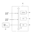
- FIG. 6 is a block diagram showing the second device control unit 82, and a program storage unit storing a program 83, a CPU 84, and a memory 85 are connected to a bus 86.
- the program 83 includes software such as a recipe for a series of processes performed in the second substrate processing apparatus 2 and a wafer W transfer recipe.
- the program 83 receives a signal that the door 92 is opened together with the lid of the FOUP 10, and associates the time at that time with the lot of the FOUP 10 that has been loaded.
- a group of steps for writing into the memory 85 is provided, and thus a detection unit for detecting the time of loading the FOUP 10 is configured.
- the program 83 includes a step group for calculating the leaving time of the FOUP 10 with reference to the unloading time transmitted from the host computer 8 (the time when the FOUP 10 is unloaded from the first substrate processing apparatus 1). Yes.
- the memory 85 stores data in which the standing time of the FOUP 10 is associated with, for example, the heating time of the second heating unit 50.
- the program 83 further includes a step group for obtaining the heating time of the second heating unit 50 based on the calculated leaving time and the data in the memory 85.
- the first device control unit 81, the host computer 8, and the second device control unit 82 also serve as a measurement unit that measures the standing time.
- the significance of adjusting the heating time of the second heating unit 50 is as follows.
- the solvent cannot completely evaporate within the realistic standing time considering the throughput. Therefore, at the time immediately before the second heating unit 50 performs the heat treatment, The solvent is contained in an amount corresponding to the length.
- the generation of acid in the resist at the time of exposure and the diffusion of acid in the resist in the heat treatment (PEB) before development are hindered, and the line width of the pattern changes according to the residual amount of solvent. Therefore, in order to make the line width uniform between the wafers W, it is necessary to make the residual amount of the solvent in the resist before the exposure uniform.
- the residual amount of the solvent in the resist in other words, the volatilization amount, is transferred to the second substrate processing apparatus 2 after the wafer W is heated by the first heating unit 6 in the first substrate processing apparatus 1. This is determined according to the standing time until the heat treatment is started in the second heating unit 50. Therefore, in order to align the amount of solvent in the resist before exposure between lots in advance before exposure, a second heating unit 50 is provided, and the second heating unit 50 supplies heating energy according to the standing time. I try to adjust it.
- the first heating unit 6 is promptly returned to the FOUP 10 after the heating process (first PAB), and in the second substrate processing apparatus 2, the FOUP 10 is promptly loaded.
- Heat treatment (second PAB) is performed in the second heating unit. Therefore, the leaving time depends on the time until the FOUP 10 is transported from the first substrate processing apparatus 1 to the second substrate processing apparatus 2, and therefore, the leaving time of the FOUP 10 is managed as described above. is doing.
- the time when the FOUP 10 is unloaded from the first substrate processing apparatus 1 (specifically, the time when the door 92 is closed) is handled as the measurement start time of the FOUP 10 leaving time.
- the above measurement start time is the time when the heating process (first PEB) is completed in the first heating unit 6, for example, the time when the wafer W of the final number of the lot is unloaded from the first heating unit 6. It may be the time when the wafer W after the first PAB is delivered to the transfer arm 93 in the carrier block B1.
- the measurement start time of the leaving time is set from the carrier standby unit 100 to the FOUP 10. It is good also as time when is carried out. Since the waiting time of the FOUP 10 in the carrier waiting unit 100 is cited as a major factor that influences the leaving time, the difference in the leaving time between lots is also reflected in this case. Therefore, in adjusting the heating time of the second PAB based on the standing time, the standing time until the FOUP 10 is carried out from the first substrate processing apparatus 1 and then carried into the second substrate processing apparatus 2 is used. It is equivalent to measuring
- the carrier transport mechanism 3 places, for example, the FOUP 10 containing 25 wafers 300 having a diameter of 300 mm on the placement stage 91 of the carrier block B1 of the first substrate processing apparatus 1.
- the wafer W is taken out from the FOUP 10 by the transfer arm 93 and placed on the shelf unit U7 (step S1).
- an SOC film which is a base film serving as an etching mask, is formed together with the resist on the wafer W, for example, in the first unit block D1, and then transferred to the third unit block D3 to form an antireflection film.
- the wafer W is loaded into, for example, the unit block D5, and a resist solution is applied (step S3).
- the wafer W coated with the resist film is transferred to the transfer arm 61 of the first heating unit 6 by the main arm A5. Thereafter, it is placed on the heating plate 62 by the transfer arm 61 and heated at, for example, 80 to 100 ° C. for 60 seconds (first PAB is performed (step S4)). As a result, the solvent contained in the resist film is volatilized. Thereafter, the wafer W is transferred from the heating plate 62 to the transfer arm 61, and then transferred to the main arm A5. Thereafter, the paper is delivered to the shelf unit U7, and then returned to the FOUP 10 by the transfer arm 93, and the door 92 is closed together with the lid portion of the FOUP 10 (step S5).
- the FOUP 10 is lifted and carried out of the carrier block B1 of the first substrate processing apparatus 1 by the carrier transport mechanism 3, for example, OHT (step S6). Further, as described above, when the lid of the FOUP 10 is closed (when the door 92 is closed), the first device control unit 81 can grasp this time, so that the time is taken as the unloading time of the FOUP 10. 8 is sent. For convenience of description, the following explanation will be made with this time as t1. Next, the FOUP 10 carried out from the first substrate processing apparatus 1 is transported to the carrier standby unit 100 and waits here (step S7).
- the number of installed first substrate processing apparatuses 1 and the number of installed second substrate processing apparatuses 2 correspond 1: 1, the number of substrates per unit time in the entire first substrate processing apparatus 1
- the number of processed sheets (throughput) is set to be larger than the number of processed substrates per unit time in the exposure apparatus B4, for example.
- the carrier standby unit 100 becomes a buffer area, and the FOUP 10 is always on standby, and the exposure apparatus B4 is fully operated.
- the overall throughput of the plurality of first substrate processing apparatuses 1 is the same as that of the exposure apparatus B4. More than the throughput is set.
- the FOUP 10 placed on the carrier standby unit 100 is lifted by the carrier transport mechanism 3 and placed on the placement stage 91 of the carrier block B1 in the second substrate processing apparatus 2 (step S8).
- the door 92 in the second substrate processing apparatus 2 is opened together with the cover of the FOUP 10, and the wafer W is taken out from the FOUP 10 (step S9).
- the FOUP 10 carried into the second substrate processing apparatus 2 is stored in the memory 85 of the second apparatus control unit 82 from the first apparatus control unit 81 via the host computer 8.
- the unloading time t1 of one substrate processing apparatus 1 is written. Since the second apparatus control unit 82 grasps the time t2 when the door 92 of the carrier block B1 of the second substrate processing apparatus 2 is opened, the time t1 is subtracted from the time t2 corresponding to the leaving time of the FOUP 10. Time ⁇ t is obtained. Further, the second device control unit 82 reads out the heat treatment time of the second heating unit 50 corresponding to the standing time ⁇ t from the data in the memory 85 and sets it as the heat treatment time of the second heating unit 50. *
- the wafer W taken out from the FOUP 10 is carried into the second heating unit 50 and heated on the heating plate for the set heat treatment time to perform the second PAB (step S10). That is, when the standing time of the FOUP 10 is long, the volatilization time of the solvent in the resist film of the wafer W in the FOUP 10 is long, so the amount of the solvent in the resist film is small, and therefore the time of the second PAB is short. Is set. On the contrary, when the standing time of the FOUP 10 is short, since the volatilization time of the solvent in the resist film is short, the amount of the solvent in the resist film is large, and therefore the time for the second PAB is set short. Therefore, the amount of the solvent in the resist film on the wafer W after the second PAB is performed is uniform among lots, or variation in the amount of the solvent is reduced.
- the wafer W is taken out from the second heating unit 50 and is carried into the exposure apparatus B4 for exposure (step S11).
- an acid is generated from the photosensitizer contained in the resist.
- the wafer W is carried into the third heating unit via the exposure apparatus B4 and the interface block B3, and is heated at, for example, 80 to 100 ° C. for 60 seconds to perform PEB.
- the acid in the resist film produced at the time of exposure diffuses and acts as a catalyst, for example, to decompose the base resin that is the main component of the resist film (step S12).
- the wafer W taken out from the third heating unit is carried into the developing unit and developed (step S13).
- the developing unit for example, the developer is supplied to the wafer W by spin coating as in the above-described resist coating unit. As a result, the portion of the resist film where the acid has diffused during PEB is dissolved, and a resist pattern is formed. Thereafter, the wafer W is returned to the FOUP 10 (step S14).
- the inside of the first and second substrate processing apparatuses 1 and 2 is made a clean atmosphere by FFU, but it is inevitable that amine is mixed in the atmosphere outside the apparatus. For this reason, the wafer W on which the resist film is formed is returned to the FOUP 10 and in an atmosphere containing amine from when it is unloaded from the first substrate processing apparatus 1 to when it is loaded into the second substrate processing apparatus 2 ( Pass through the atmosphere).
- the amount of amine mixed is very small. For example, for chemically amplified resists, even a small amount of amine significantly inhibits acid diffusion. Therefore, even if the first substrate processing apparatus 1 has already applied the resist solution and the PAB is performed, the second substrate processing apparatus 2 that is the transport destination of the FOUP 10 uses the second PAB before the exposure. By performing the steps, the amine in the resist film is scattered and disappears, development defects can be prevented, and variations in pattern line width can be suppressed. In addition, after the FOUP 10 is unloaded from the first substrate processing apparatus 1, the standing time until the FOUP 10 is loaded into the second substrate processing apparatus 2 is measured.
- the heating time of the second PAB which is a heating process performed by the second heating unit 50 of the second substrate processing apparatus 2 is adjusted. For this reason, variation in the residual amount of the solvent in the resist film between lots of wafers W can be suppressed, and the resist pattern forming process can be stabilized.
- the heating temperature may be adjusted based on the above-described leaving time. As shown in a verification test described later, the line width of the resist pattern can be adjusted by adjusting the heating temperature of the second heating unit 50. Therefore, the same effect can be obtained in this case.
- the heating temperature is adjusted in this way, data in which the standing time is associated with the heating temperature is stored in advance in the memory 85. Note that both the heating time and the heating temperature may be adjusted according to the standing time. In this case, data in which the leaving time is associated with the heating time and the heating temperature is stored in the memory 85. Will be remembered.
- the abandoned time described above is not limited to measurement, but may be obtained by prediction.
- the time taken out from the carrier standby unit 100 can be predicted according to the number of FOUPs 10 that are already on standby, for example, the host computer 8 can wait for the FOUP 10
- the standing time may be predicted based on the number of units.
- the predicted leaving time is transmitted from the host computer 8 to the second device control unit 82.
- the heating energy of the second PAB is adjusted according to the leaving time. It does not have to be.
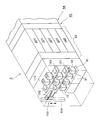
- FIG. 8 shows a configuration example in such a case, and a plurality of, for example, two-stage shelves 101 are provided above the placement stage 91 in the carrier block B1 of the second substrate processing apparatus 2, A placement stage 102 for placing a carrier on each shelf 101 is provided.
- the arrangement of the lowermost mounting stages 91 corresponds to the carrier block B 1
- the mounting stage 102 provided with the upper two shelves 101 corresponds to the carrier standby unit 100.
- a carrier delivery mechanism 103 for moving the FOUP 10 between the placement stages 91 and 102 is provided.
- the carrier delivery mechanism 103 includes a horizontal guide (not shown) that extends along the mounting stage 102 that moves up and down along the lifting guide 104, and a joint arm that is configured to be movable along the horizontal guide and holds the head portion 110 of the FOUP 10. 105.
- a horizontal guide (not shown) that extends along the mounting stage 102 that moves up and down along the lifting guide 104, and a joint arm that is configured to be movable along the horizontal guide and holds the head portion 110 of the FOUP 10. 105.
- the FOUP 10 is transferred by the carrier transfer mechanism 103 to the mounting stage 91 of the lowest shelf corresponding to the carrier block B1, and the wafer W in the FOUP 10 is taken out.
- the substrate processing method is such that acid is generated in the exposed region of the resist film and the resist film is dissolved, but the substrate in which the exposed region of the resist film is insolubilized by the acid. It may be a processing method. Further, in the second heating unit 50, the second PAB and PEB may be performed. [Verification test]
- the relationship between the aforementioned standing time and the CD (critical dimension) of the resist pattern according to the set temperature of the second heating unit 50 was examined as follows. Using the substrate processing system according to the above-described embodiment, the heating time of the second heating unit was set to 60 seconds. The heating temperature of the second heating unit is set to three kinds of 80 ° C., 77.5 ° C., and 75 ° C., and the standing time (the time that the FOUP 10 is left outside the first substrate processing apparatus 1 under each temperature condition) ) was set in three ways of 3, 6, and 12 hours. Then, after each wafer W was heat-treated by the second heating unit 50, exposure and development were performed, and the line width of the pattern was measured. In addition, an example in which the resist film is formed and the FOUP 10 containing the wafer W is first unloaded from the first substrate processing apparatus 1 and immediately loaded into the second substrate processing apparatus 2 is shown as 0 for the sake of convenience.
- FIG. 9 shows this result, and shows the relationship between the standing time and the resist pattern CD when the heating temperature of the second heating unit 50 is set to 80 ° C., 77.5 ° C., and 75 ° C., respectively. According to this result, it can be seen that the CD becomes thicker as the leaving time becomes longer. From the graph of FIG. 9, the resist used in the above-described example is applied to the wafer W and heated (after the first PAB is performed), even if a time as long as 6 hours elapses. Further, it can be seen that the CD becomes larger with the elapsed time thereafter. Further, it is sufficiently predicted that the solvent amount does not become a constant value even after 12 hours.
- the amount of the solvent changes depending on the standing time after the first PAB is performed in this resist. Therefore, in the second substrate processing apparatus 2, by the heating energy corresponding to the standing time, It is understood that it is effective to perform the second PAB. It can also be seen that the CD is reduced by lowering the heating temperature by the second heating unit 50. By raising the heating temperature, the solvent contained in the resist film is volatilized, and the diffusion length of the acid when PEB is performed is shortened, so that the CD is estimated to increase.
Landscapes
- General Physics & Mathematics (AREA)
- Physics & Mathematics (AREA)
- Engineering & Computer Science (AREA)
- Health & Medical Sciences (AREA)
- Epidemiology (AREA)
- Environmental & Geological Engineering (AREA)
- Public Health (AREA)
- Toxicology (AREA)
- Atmospheric Sciences (AREA)
- Life Sciences & Earth Sciences (AREA)
- Computer Networks & Wireless Communication (AREA)
- Container, Conveyance, Adherence, Positioning, Of Wafer (AREA)
- Exposure Of Semiconductors, Excluding Electron Or Ion Beam Exposure (AREA)
Abstract
Description
このような塗布、現像処理を行う基板処理システムにおいてレジスト液などの、塗布液を塗布する塗布モジュールに用いる処理液は固着しやすいものが多く、付着したときに汚れが取りにくく、露光装置や、現像モジュールに比べてメンテナンスに時間がかかり、スループットの制約になる。そのため塗布モジュールを備えた前段側の装置と、露光装置に接続される現像モジュールを含む後段側の装置と、を分離して別個の装置構成とし、塗布モジュールのメンテナンスを行っている際にも露光、現像処理を行うことができるようにした構成が知られている(特許文献1)。
次いで、第1の基板処理装置にて基板を加熱処理する工程と、
その後、前記基板をキャリアに収納し、第1の基板処理装置のキャリアブロックから第2の基板処理装置のキャリアブロックに搬送する工程と、
前記第1の基板処理装置のキャリアブロックからキャリアが搬出された後、第2の基板処理装置のキャリアブロックに当該キャリアが搬入されるまでの時間を含む基板の放置時間に基づいて、加熱時間及び加熱温度の少なくとも一方を調整した状態で前記第2の基板処理装置にて基板を加熱処理する工程と、
続いて前記基板を露光し、更に前記第2の基板処理装置にて加熱処理した後、現像する工程と、を含むことを特徴とする。
前記第1の基板処理装置から搬出されたキャリアが搬入されるキャリアブロックと、このキャリアブロックに搬入されたキャリアから取り出された基板を加熱処理する第2の加熱ユニットと、この第2の加熱ユニットにて加熱処理され、次いで露光された基板を加熱処理するための第3の加熱ユニットと、この第3の加熱ユニットにて加熱処理された基板を現像する現像ユニットと、を含み、露光装置に接続される第2の基板処理装置と、
前記第1の基板処理装置のキャリアブロックからキャリアが搬出された後、第2の基板処理装置のキャリアブロックに当該キャリアが搬入されるまでの時間を含む基板の放置時間に基づいて、前記第2の加熱ユニットにおける加熱時間及び加熱温度の少なくとも一方を調整する加熱調整部と、を備えたことを特徴とする。
またキャリア搬送機構3の搬送路の途中には、例えば複数のFOUP10を一時的に載置しておくためのキャリア待機部100が設けられており、第1の基板処理装置1から搬出されたFOUP10は、例えば第2の基板処理装置2に搬入される前に一旦キャリア待機部100に載置される。
また第2の基板処理装置2の天井部にも、第1の基板処理装置1と同様にFFUが設けられ、第2の基板処理装置2内の雰囲気が清浄に保たれている。
また第1の基板処理装置1からFOUP10が搬出された後、第2の基板処理装置2に当該FOUP10が搬入されるまでの放置時間を計測している。そしてこの放置時間に基づいて、第2の基板処理装置2の第2の加熱ユニット50にて行われる加熱処理である第2のPABの加熱時間を調整している。このためウエハWのロット間においてレジスト膜中の溶剤の残留量のばらつきが抑えられ、レジストパターンの形成処理の安定化を図ることができる。
更にまた、工場を稼働したときの通常の放置時間程度の短い時間でレジスト膜中の溶剤量が一定化するレジストを用いる場合には、放置時間に応じて第2のPABの加熱エネルギーを調整しなくてもよい。
さらに上述の実施の形態においては、レジスト膜の露光された領域に酸が発生し、レジスト膜が溶解する基板処理方法であったが、レジスト膜の露光された領域が酸により、不可溶化する基板処理方法であってもよい。
さらに第2の加熱ユニット50において、第2のPABと、PEBとを行ってもよい。
[検証試験]
この結果によれば、放置時間が長くなるに従いCDが太くなっていることが分かる。
図9のグラフから、既述の例に用いたレジストは、ウエハWに塗布されて加熱処理された後(第1のPABが行われた後)において、6時間もの長い時間が経過しても、更にその後の経過時間によりCDが大きくなっていることが分かる。また12時間を経過してもまだ溶剤量が一定値にならないことが十分予測される。従ってこのレジストは、第1のPABを行った後の放置時間に応じて溶剤の量が変わるということが分かり、このため第2の基板処理装置2にて、放置時間に応じた加熱エネルギーにより、第2のPABを行うことが有効であることが理解される。
また第2の加熱ユニット50による加熱温度を下げることでCDが小さくなることが分かる。加熱温度を上げることによりレジスト膜に含まれる溶剤が揮発し、PEBを行った時の酸の拡散長が短くなるためCDが大きくなると推測される。
2 第2の基板処理装置
3 キャリア搬送機構
5 レジスト塗布ユニット
6 第1の加熱ユニット
8 上位コンピュータ
81 第1の装置制御部
82 第2の装置制御部
10 FOUP
100 キャリア待機部
W ウエハ
Claims (10)
- 第1の基板処理装置にて基板にレジストを塗布する工程と、
次いで、第1の基板処理装置にて基板を加熱処理する工程と、
その後、前記基板をキャリアに収納し、第1の基板処理装置のキャリアブロックから第2の基板処理装置のキャリアブロックに搬送する工程と、
前記第1の基板処理装置のキャリアブロックからキャリアが搬出された後、第2の基板処理装置のキャリアブロックに当該キャリアが搬入されるまでの時間を含む基板の放置時間に基づいて、加熱時間及び加熱温度の少なくとも一方を調整した状態で前記第2の基板処理装置にて基板を加熱処理する工程と、
続いて前記基板を露光し、更に前記第2の基板処理装置にて加熱処理した後、現像する工程と、を含むことを特徴とする基板処理方法。 - 前記第1の基板処理装置のキャリアブロックからキャリアが搬出された後、第2の基板処理装置のキャリアブロックに当該キャリアが搬入されるまでの時間を含む基板の放置時間を計測する工程を含むことを特徴とする請求項1記載の基板処理方法。
- 前記第1の基板処理装置のキャリアブロックからキャリアが搬出された後、第2の基板処理装置のキャリアブロックに当該キャリアが搬入されるまでの間に、キャリアがキャリア待機部に待機する工程を含むことを特徴とする請求項2または3に記載の基板処理方法。
- 基板を収納して搬送するキャリアが搬入出されるキャリアブロックと、このキャリアブロックに搬入されたキャリアから取り出された基板に対してレジスト膜が塗布されるレジスト塗布ユニットと、レジストが塗布された基板を加熱処理する第1の加熱ユニットと、を含む第1の基板処理装置と、
前記第1の基板処理装置から搬出されたキャリアが搬入されるキャリアブロックと、このキャリアブロックに搬入されたキャリアから取り出された基板を加熱処理する第2の加熱ユニットと、この第2の加熱ユニットにて加熱処理され、次いで露光された基板を加熱処理するための第3の加熱ユニットと、この第3の加熱ユニットにて加熱処理された基板を現像する現像ユニットと、を含み、露光装置に接続される第2の基板処理装置と、
前記第1の基板処理装置のキャリアブロックからキャリアが搬出された後、第2の基板処理装置のキャリアブロックに当該キャリアが搬入されるまでの時間を含む基板の放置時間に基づいて、前記第2の加熱ユニットにおける加熱時間及び加熱温度の少なくとも一方を調整する加熱調整部と、を備えたことを特徴とする基板処理システム。 - 前記第1の基板処理装置にて処理された基板が収納されたキャリアを第1の基板処理装置のキャリアブロックから第2の基板処理装置のキャリアブロックに搬送するキャリア搬送機構を備えたことを特徴とする請求項4記載の基板処理システム。
- 前記第1の基板処理装置のキャリアブロックから搬出されたキャリアが第2の基板処理装置のキャリアブロックに搬入される前に一時的に置かれるキャリア待機部を備えたことを特徴とする請求項5記載の基板処理システム。
- 前記第2の基板処理装置は、前記キャリア待機部と、当該キャリア待機部と当該第2の基板処理装置のキャリアブロックとの間でキャリアの受け渡しを行うキャリア受け渡し機構と、を備えたことを特徴とする請求項6記載の基板処理システム。
- 前記放置時間を計測する計測部を備えたことを特徴とする請求項4ないし7のいずれか一項に記載の基板処理システム。
- 基板にレジスト膜を形成するための基板処理装置であって、
請求項4ないし8のいずれか一項に記載された基板処理システムに用いられる第1の基板処理装置であることを特徴とする基板処理装置。 - レジスト膜が形成された基板を露光装置に受け渡し、露光装置にて露光された基板を現像するための基板処理装置であって、
請求項4ないし8のいずれか一項に記載された基板処理システムに用いられる第2の基板処理装置であることを特徴とする基板処理装置。
Priority Applications (4)
| Application Number | Priority Date | Filing Date | Title |
|---|---|---|---|
| US15/565,714 US10520831B2 (en) | 2015-04-16 | 2016-03-28 | Substrate processing method, substrate processing system and substrate processing apparatus |
| KR1020177029497A KR102568357B1 (ko) | 2015-04-16 | 2016-03-28 | 기판 처리 방법, 기판 처리 시스템 및 기판 처리 장치 |
| KR1020237027631A KR102695211B1 (ko) | 2015-04-16 | 2016-03-28 | 기판 처리 방법, 기판 처리 시스템 및 기판 처리 장치 |
| CN201680022298.3A CN107533955B (zh) | 2015-04-16 | 2016-03-28 | 基板处理方法和基板处理系统 |
Applications Claiming Priority (4)
| Application Number | Priority Date | Filing Date | Title |
|---|---|---|---|
| JP2015-084406 | 2015-04-16 | ||
| JP2015084406 | 2015-04-16 | ||
| JP2016011544A JP6512119B2 (ja) | 2015-04-16 | 2016-01-25 | 基板処理方法、基板処理システム及び基板処理装置 |
| JP2016-011544 | 2016-01-25 |
Publications (1)
| Publication Number | Publication Date |
|---|---|
| WO2016167105A1 true WO2016167105A1 (ja) | 2016-10-20 |
Family
ID=57126186
Family Applications (1)
| Application Number | Title | Priority Date | Filing Date |
|---|---|---|---|
| PCT/JP2016/059808 Ceased WO2016167105A1 (ja) | 2015-04-16 | 2016-03-28 | 基板処理方法、基板処理システム及び基板処理装置 |
Country Status (2)
| Country | Link |
|---|---|
| KR (1) | KR102695211B1 (ja) |
| WO (1) | WO2016167105A1 (ja) |
Families Citing this family (1)
| Publication number | Priority date | Publication date | Assignee | Title |
|---|---|---|---|---|
| KR102884391B1 (ko) * | 2023-11-16 | 2025-11-12 | 세메스 주식회사 | 기판 처리 장치 및 기판 처리 방법 |
Citations (6)
| Publication number | Priority date | Publication date | Assignee | Title |
|---|---|---|---|---|
| JPH08172046A (ja) * | 1994-12-16 | 1996-07-02 | Nippon Steel Corp | 半導体製造装置 |
| JPH1130868A (ja) * | 1997-07-10 | 1999-02-02 | Toshiba Corp | パタン形成方法 |
| JP2001338865A (ja) * | 2000-05-30 | 2001-12-07 | Nec Corp | 半導体露光方法及び半導体製造装置 |
| JP2002214802A (ja) * | 2001-01-12 | 2002-07-31 | Hitachi Ltd | 半導体装置の製造方法 |
| JP2007101738A (ja) * | 2005-09-30 | 2007-04-19 | Dainippon Printing Co Ltd | レジスト基板、レジストパターン形成方法及びレジスト基板の保存方法 |
| JP2011204774A (ja) * | 2010-03-24 | 2011-10-13 | Toshiba Corp | パターン形成方法および脱水装置 |
Family Cites Families (1)
| Publication number | Priority date | Publication date | Assignee | Title |
|---|---|---|---|---|
| JP4849969B2 (ja) | 2006-06-15 | 2012-01-11 | 東京エレクトロン株式会社 | 基板処理システムおよび基板搬送方法 |
-
2016
- 2016-03-28 WO PCT/JP2016/059808 patent/WO2016167105A1/ja not_active Ceased
- 2016-03-28 KR KR1020237027631A patent/KR102695211B1/ko active Active
Patent Citations (6)
| Publication number | Priority date | Publication date | Assignee | Title |
|---|---|---|---|---|
| JPH08172046A (ja) * | 1994-12-16 | 1996-07-02 | Nippon Steel Corp | 半導体製造装置 |
| JPH1130868A (ja) * | 1997-07-10 | 1999-02-02 | Toshiba Corp | パタン形成方法 |
| JP2001338865A (ja) * | 2000-05-30 | 2001-12-07 | Nec Corp | 半導体露光方法及び半導体製造装置 |
| JP2002214802A (ja) * | 2001-01-12 | 2002-07-31 | Hitachi Ltd | 半導体装置の製造方法 |
| JP2007101738A (ja) * | 2005-09-30 | 2007-04-19 | Dainippon Printing Co Ltd | レジスト基板、レジストパターン形成方法及びレジスト基板の保存方法 |
| JP2011204774A (ja) * | 2010-03-24 | 2011-10-13 | Toshiba Corp | パターン形成方法および脱水装置 |
Also Published As
| Publication number | Publication date |
|---|---|
| KR102695211B1 (ko) | 2024-08-14 |
| KR20230124759A (ko) | 2023-08-25 |
Similar Documents
| Publication | Publication Date | Title |
|---|---|---|
| JP6512119B2 (ja) | 基板処理方法、基板処理システム及び基板処理装置 | |
| KR102436241B1 (ko) | 기판 처리 방법 및 열처리 장치 | |
| KR102503838B1 (ko) | 기판 가열 장치 | |
| JP4535499B2 (ja) | 加熱装置、塗布、現像装置及び加熱方法 | |
| CN101034661B (zh) | 基板处理装置和基板处理条件研究方法 | |
| TW202447841A (zh) | 基板處理系統及基板處理方法 | |
| JP2002184671A (ja) | 基板処理システム及び基板処理方法 | |
| JP4279102B2 (ja) | 基板処理装置及び基板処理方法 | |
| CN107924857A (zh) | 保管装置和保管方法 | |
| WO2008059684A1 (fr) | Equipement de transport de substrat | |
| JP2003224175A (ja) | 基板処理装置および基板処理方法 | |
| JP5578675B2 (ja) | レジストパターン形成装置 | |
| US12035576B2 (en) | Substrate treating apparatus and substrate transporting method | |
| KR20170055819A (ko) | 기판 처리 장치 | |
| CN111048445B (zh) | 加热板冷却方法及基板处理装置 | |
| JP2002043208A (ja) | 塗布現像処理方法 | |
| WO2016167105A1 (ja) | 基板処理方法、基板処理システム及び基板処理装置 | |
| JP5936853B2 (ja) | 基板処理装置および基板処理方法 | |
| JP4584872B2 (ja) | 基板処理システムおよび基板搬送方法 | |
| KR20190089546A (ko) | 기판 처리 장치 및 방법 | |
| CN101325149B (zh) | 用于半导体制造的系统、方法及半导体制造的装置 | |
| JP5579991B2 (ja) | 基板処理装置および基板処理方法 | |
| JP2010074185A (ja) | 加熱装置、塗布、現像装置及び加熱方法 | |
| JPH04262555A (ja) | 処理装置 | |
| JP2011210814A (ja) | 基板処理ユニット、基板処理方法および基板処理装置 |
Legal Events
| Date | Code | Title | Description |
|---|---|---|---|
| 121 | Ep: the epo has been informed by wipo that ep was designated in this application |
Ref document number: 16779896 Country of ref document: EP Kind code of ref document: A1 |
|
| WWE | Wipo information: entry into national phase |
Ref document number: 15565714 Country of ref document: US |
|
| ENP | Entry into the national phase |
Ref document number: 20177029497 Country of ref document: KR Kind code of ref document: A |
|
| NENP | Non-entry into the national phase |
Ref country code: DE |
|
| 122 | Ep: pct application non-entry in european phase |
Ref document number: 16779896 Country of ref document: EP Kind code of ref document: A1 |