WO2016167095A1 - プレスフィット端子及び基板用コネクタ - Google Patents
プレスフィット端子及び基板用コネクタ Download PDFInfo
- Publication number
- WO2016167095A1 WO2016167095A1 PCT/JP2016/059325 JP2016059325W WO2016167095A1 WO 2016167095 A1 WO2016167095 A1 WO 2016167095A1 JP 2016059325 W JP2016059325 W JP 2016059325W WO 2016167095 A1 WO2016167095 A1 WO 2016167095A1
- Authority
- WO
- WIPO (PCT)
- Prior art keywords
- press
- contact portion
- contact
- fit terminal
- hole
- Prior art date
- Legal status (The legal status is an assumption and is not a legal conclusion. Google has not performed a legal analysis and makes no representation as to the accuracy of the status listed.)
- Ceased
Links
Images




Classifications
-
- H—ELECTRICITY
- H01—ELECTRIC ELEMENTS
- H01R—ELECTRICALLY-CONDUCTIVE CONNECTIONS; STRUCTURAL ASSOCIATIONS OF A PLURALITY OF MUTUALLY-INSULATED ELECTRICAL CONNECTING ELEMENTS; COUPLING DEVICES; CURRENT COLLECTORS
- H01R12/00—Structural associations of a plurality of mutually-insulated electrical connecting elements, specially adapted for printed circuits, e.g. printed circuit boards [PCB], flat or ribbon cables, or like generally planar structures, e.g. terminal strips, terminal blocks; Coupling devices specially adapted for printed circuits, flat or ribbon cables, or like generally planar structures; Terminals specially adapted for contact with, or insertion into, printed circuits, flat or ribbon cables, or like generally planar structures
- H01R12/70—Coupling devices
- H01R12/7005—Guiding, mounting, polarizing or locking means; Extractors
- H01R12/7011—Locking or fixing a connector to a PCB
- H01R12/7064—Press fitting
-
- H—ELECTRICITY
- H01—ELECTRIC ELEMENTS
- H01R—ELECTRICALLY-CONDUCTIVE CONNECTIONS; STRUCTURAL ASSOCIATIONS OF A PLURALITY OF MUTUALLY-INSULATED ELECTRICAL CONNECTING ELEMENTS; COUPLING DEVICES; CURRENT COLLECTORS
- H01R12/00—Structural associations of a plurality of mutually-insulated electrical connecting elements, specially adapted for printed circuits, e.g. printed circuit boards [PCB], flat or ribbon cables, or like generally planar structures, e.g. terminal strips, terminal blocks; Coupling devices specially adapted for printed circuits, flat or ribbon cables, or like generally planar structures; Terminals specially adapted for contact with, or insertion into, printed circuits, flat or ribbon cables, or like generally planar structures
- H01R12/50—Fixed connections
- H01R12/51—Fixed connections for rigid printed circuits or like structures
- H01R12/55—Fixed connections for rigid printed circuits or like structures characterised by the terminals
- H01R12/58—Fixed connections for rigid printed circuits or like structures characterised by the terminals terminals for insertion into holes
- H01R12/585—Terminals having a press fit or a compliant portion and a shank passing through a hole in the printed circuit board
Definitions
- the present invention relates to a press-fit terminal and a board connector.
- each contact portion 114A of each facing portion 114 elastically contacts the inner peripheral surface of the through hole 122, a contact pressure is applied from each contact portion 114A to the inner peripheral surface.
- the layer constituting the circuit board may be peeled off in the vicinity of the portion of the circuit board where the contact pressure is applied, and the surface may be whitened (part indicated by reference numeral D11 in FIG. 7).
- substrate damage part As shown in FIG. 7, when the pitch between the adjacent through holes 122 is narrow, the substrate damage portions D11 may be close to or in contact with each other, and the insulating performance between the adjacent through holes 122 may be deteriorated.
- Patent Document 1 discloses a press-fit terminal that suppresses a decrease in insulation performance between adjacent through holes.
- This press-fit terminal is characterized by the size in the width direction of each facing portion and the length in the press-fitting direction of each facing portion, so that the contact applied to the through hole when the press-fit terminal is press-fitted into the through hole.
- the pressure is reduced to reduce damage (whitening due to peeling of the layer) applied to the substrate from the contact portion of each facing portion.
- the present invention has been created in view of the above-described problems, and an object thereof is to suppress a decrease in insulation performance while ensuring connection reliability.
- the technology disclosed in the present specification is a press-fit terminal that is held in a through hole that is inserted in a through hole provided in a plate along the insertion direction, and an inner peripheral surface of the through hole.
- a first contact portion and a second contact portion that are in elastic contact with each other, and in a cross-sectional view perpendicular to the insertion direction, the radius of curvature of the second contact portion is divided by the radius of curvature of the first contact portion. It relates to a press-fit terminal having a measured value of 0.75 or less.
- the radius of curvature of the first contact portion is larger than the radius of curvature of the second contact portion and becomes a gentle arc shape in the cross-sectional view. Therefore, when contacting the inner peripheral surface of the through hole The contact pressure applied to the inner peripheral surface is smaller than the other, and damage to the substrate is small.
- the second contact portion having a smaller radius of curvature than the first contact portion has a larger contact pressure applied to the inner peripheral surface when contacting the inner peripheral surface of the through hole than the first contact portion. Sufficient connection reliability can be ensured between the press-fit terminal and the through-hole without reducing the holding force of the press-fit terminal held inside.
- each of the adjacent through holes is provided.
- the first contact part of one press-fit terminal and the second contact part of the other press-fit terminal are adjacent between adjacent through holes. That is, a contact portion having a small contact pressure applied to the inner peripheral surface and a contact portion having a large contact pressure applied to the inner peripheral surface are adjacent to each other between adjacent through holes.
- a contact portion with a small damage to the substrate and a contact portion with a large damage to the substrate are adjacent to each other.
- the press-fit terminal has a pair of facing portions arranged in a facing manner, and the first contact portion and the second contact portion are provided in each of the pair of facing portions and orthogonal to the insertion direction.
- the line segment connecting the first contact portions and the line segment connecting the second contact portions may intersect between the pair of opposed portions.
- the first contact portion and the second contact portion are arranged alternately between the pair of facing portions in a cross-sectional view of the cross section orthogonal to the insertion direction. For this reason, when the press-fit terminal is inserted into each of the adjacent through holes, a contact portion that is small in damage to the substrate and a contact portion that is large in damage to the substrate are adjacent between the adjacent through holes.
- a typical configuration can be provided.
- Another technique disclosed in the present specification relates to a board connector having the press-fit terminal connected to the terminal insertion hole of the board and a housing capable of accommodating a plurality of the press-fit terminals.
- FIG. 1 a board connector 1 and a press-fit terminal 10 extending from the board connector 1 are illustrated.
- the board connector 1 is used as an in-vehicle electronic control device, and is made of a resin housing 4, a plurality of press-fit terminals 10 housed in the housing 4 and bent and extended in an L shape from the housing 4. Is provided.
- Each press-fit terminal 10 is formed in an elongated tab shape by pressing a metal plate material having excellent conductivity such as a copper alloy (see FIG. 2).
- each press-fit terminal 10 is attached to the housing 4 of the board connector 1 by press-fitting or the like, and the other end is attached to a circuit board 20 (an example of a board, see FIG. 4) incorporated in an in-vehicle electronic device. It is inserted (press-fit) into the provided through hole 22.
- the direction in which the press-fit terminal 10 is inserted into the through hole 22 is defined as the lower direction, and the opposite direction is defined as the upper direction.
- the horizontal direction in FIGS. 2 and 4 is defined as the width direction of the press-fit terminal 10.
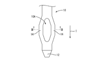
- each press-fit terminal 10 has a leading end that tapers into a guide portion 12 that guides the press-fit terminal 10 to the through hole 22.
- a pair of opposing portions 14 that are arranged in an opposing manner in the width direction across the slit 10 ⁇ / b> A and that can be elastically deformed are provided.
- Each press-fit terminal 10 is press-fitted into the through-hole 22 so that the pair of opposed portions 14 are pressed against the inner peripheral surface of the through-hole 22 to be elastically deformed inward and are held in the through-hole 22.
- Each of the pair of facing portions 14 is a rectangular side (as opposed to the side facing the other facing portion 14), as shown in FIG. 3, as viewed in a cross section orthogonal to the insertion direction of the press-fit terminal 10.
- the two corners on both sides of the side) are chamfered to form a substantially rectangular shape with a curvature, and the center position between the opposing portions 14 (the position indicated by C1 in FIG. 3). It is a point-symmetric arrangement as a symmetry point.
- Two portions of each facing portion 14 provided with the curvature are a first contact portion 14A and a second contact portion 14B, respectively.
- the first contact portion 14 ⁇ / b> A and the second contact portion 14 ⁇ / b> B elastically contact the inner peripheral surface of the through hole 22 when the press-fit terminal 10 is inserted into the through hole 22.
- the curvature radius of the first contact portion 14A is different from the curvature radius of the second contact portion 14B.
- the curvature radius of the first contact portion 14A is such that the value obtained by dividing the curvature radius of the second contact portion 14B by the curvature radius of the first contact portion 14A is 0.75 or less. It is made larger than the curvature radius of the 2nd contact part 14B. Since both opposing portions 14 have point-symmetric shapes as described above, a line segment connecting the first contact portions 14A between the pair of opposing portions 14 and the second as shown in FIG. A line segment connecting the contact portions 14B intersects.
- the press-fit terminal 10 is inserted into the through hole 22 and the first contact portion 14A and the second contact portion 14B. Is elastically brought into contact with the inner peripheral surface of the through-hole 22, the contact pressure applied from the second contact portion 14B to the inner peripheral surface is more local than the contact pressure applied from the first contact portion 14A to the inner peripheral surface. Contact pressure is applied. For this reason, compared with the contact pressure applied to the inner peripheral surface from the first contact portion 14A, a larger contact pressure is applied to the inner peripheral surface from the second contact portion 14B, and the second contact portion 14B is applied to the inner peripheral surface. On the other hand, it is held well. As a result, a decrease in holding force of the press-fit terminal 10 held in the through hole 22 is suppressed.
- the contact pressure applied from the first contact portion 14A to the inner peripheral surface of the through hole 22 is applied from the second contact portion 14B to the inner peripheral surface.
- the damage that the circuit board 20 receives in the vicinity of the portion to which the contact pressure is applied from the first contact portion 14A is that the circuit board 20 is in the vicinity of the portion to which the contact pressure is applied from the second contact portion 14B. Small compared to the damage taken.
- the press-fit terminal 10 of this embodiment will be described.
- the case where the press fit terminal 10 is inserted in the through hole 22 of the circuit board 20 (refer FIG. 4) by which the pitch P between the adjacent through holes 22 was made into the narrow pitch is illustrated.
- a conductive path 24 having a contact portion subjected to a plating process or the like is provided on the inner peripheral surface of the through hole 22.
- the press-fit terminal 10 When the press-fit terminal 10 is inserted into the through hole 22 of the circuit board 20 from the guide portion 12 side along the insertion direction, the first contact portion 14A and the second contact portion 14B of each facing portion 14 are at the opening end of the through hole 22. It hits and is pressed. Then, by further inserting the press-fit terminal into the through hole 22, the first contact portion 14A and the second contact portion 14B of each facing portion 14 enter the through hole 22 while elastically deforming, and the inside of the through hole 22 Elastically contacts the peripheral surface (contact portion of the conductive path 24). Thereby, the press-fit terminal 10 is electrically connected to the conductive path 24 of the circuit board 20.
- both the facing portions 14 are slightly It becomes a distorted shape.
- first substrate damage portion when the first contact portion 14A and the second contact portion 14B are in contact with the inner peripheral surface of the through hole 22, the damage received by the circuit board 20 due to the contact pressure is greater than that from the second contact portion 14B.
- One contact portion 14A is smaller. For this reason, as shown in FIG. 5, a region of the circuit board 20 that is damaged by the contact pressure applied from the first contact portion 14 ⁇ / b> A (a portion indicated by reference numeral D ⁇ b> 2 in FIG. 5. Is smaller than a region that is damaged by contact pressure applied from the second contact portion 14B (a portion indicated by reference numeral D1 in FIG. 5; hereinafter referred to as a “first substrate damage portion”).
- the second contact portion 14B is favorably held with respect to the inner peripheral surface by applying a larger contact pressure from the second contact portion 14B to the inner peripheral surface of the through hole 22. Is done. For this reason, sufficient connection reliability can be ensured between the press-fit terminal 10 and the through hole 22 without reducing the holding force of the press-fit terminal 10 held in the through hole 22. As described above, in the press-fit terminal 10 of the present embodiment, it is possible to suppress a decrease in insulation performance while ensuring connection reliability.
- each opposing part 14 of the press fit terminal 10 is a complicated shape (for example, polygonal view sectional shape).
- each opposing part 14 of the press-fit terminal 10 of this embodiment is a substantially rectangular shape in sectional view in which a curvature is provided by chamfering a part as described above, each opposing part 14 There is no need for complicated processing to form the film. For this reason, the press fit terminal 10 of this embodiment is realizable irrespective of the size of the pitch between the adjacent through holes 22.
- each facing portion of the press-fit terminal has a substantially rectangular shape in sectional view
- shape of each facing portion in sectional view is not limited.
- the configuration in which the gap between the pair of facing portions in the press-fit terminal is a slit is illustrated, but the configuration between the pair of facing portions is not limited.
- an elastic member may be disposed between the pair of opposing portions, and thereby each opposing portion may be configured to elastically contact the inner peripheral surface of the through hole.
- the press-fit terminals exemplified in the embodiment are inserted into two adjacent through holes provided on the circuit board, respectively, and left in a high-temperature and high-humidity environment for a certain period of time with a DC voltage applied between both terminals. After that, an endurance test was performed to evaluate the insulation performance between adjacent through holes.
- PSL-2SPH manufactured by Espec is used as a constant temperature and humidity chamber, and the temperature condition is 38 to 87 ° C., the humidity condition is 82 to 96% RH, and applied between both terminals in accordance with the JPCA standard.
- the voltage was DC 5 to 100 V, and the test time was 1000 hr at maximum.
- the evaluation was made by changing between them.
Landscapes
- Coupling Device And Connection With Printed Circuit (AREA)
- Multi-Conductor Connections (AREA)
Abstract
基板に設けられたスルーホール(22)に挿入方向に沿って挿入されることでスルーホール(22)内に保持されるプレスフィット端子であって、スルーホール(22)の内周面に弾性的に接触する第1接触部(14A)及び第2接触部(14B)を有し、挿入方向と直交する断面の断面視において、第2接触部(14B)の曲率半径を第1接触部(14A)の曲率半径で除した値が0.75以下である。隣接するプレスフィット端子の間で第1接触部(14A)と第2接触部(14B)とが隣接するように第1接触部(14A)及び第2接触部(14B)を設けることで、隣接するスルーホール(22)の間で内周面に加わる接圧が小さい接触部と内周面に加わる接圧が大きい接触部とが隣接する。その結果、隣接するスルーホール(22)の間で基板のダメージを受けた部分(D1,D2)が近接することを抑制することができる。
Description
本発明は、プレスフィット端子及び基板用コネクタに関する。
従来、電子機器に組み込まれる回路基板のスルーホール122(図7参照)に圧入されることで当該スルーホール122に保持され、回路基板上の導電回路と電気的に接続されるプレスフィット端子が知られている。この種のプレスフィット端子では、スルーホール122に保持される部分に、スリット110Aを挟んで幅方向に対向状に配された一対の対向部114が設けられている。各対向部114はスリット110Aを挟んで対称形状とされ、プレスフィット端子110がスルーホール122に圧入されると、各対向部114の接触部114Aがスルーホール122の内周面に弾性的に接触する。
各対向部114の接触部114Aがスルーホール122の内周面に弾性的に接触すると、各接触部114Aから当該内周面に対して接圧が加わる。この接圧の大きさによっては、回路基板のうち当該接圧が加わった部位の近傍において回路基板を構成する層が剥離し、その表面が白化することがある(図7の符号D11で示す部分。以下、「基板ダメージ部」と称する)。このため、図7に示すように、隣接するスルーホール122間のピッチが狭い場合、基板ダメージ部D11同士が近接又は接触し、隣接するスルーホール122間の絶縁性能が低下することがある。
そこで下記特許文献1には、隣接するスルーホール間の絶縁性能の低下を抑制するプレスフィット端子が開示されている。このプレスフィット端子では、各対向部の幅方向の大きさ、及び各対向部の圧入方向における長さに特徴を設けることで、プレスフィット端子がスルーホールに圧入された際にスルーホールに加わる接圧を小さくし、各対向部の接触部から基板に加わるダメージ(上記層の剥離による白化)を軽減している。
しかしながら、プレスフィット端子がスルーホールに圧入された際にスルーホールに加わる接圧が小さくなると、スルーホール内に保持されるプレスフィット端子の保持力が低下し、プレスフィット端子とスルーホールが設けられた回路基板との間で十分な接続信頼性を確保できない虞がある。
本発明は、上記の課題に鑑みて創作されたものであって、接続信頼性を確保しながら、絶縁性能の低下を抑制することを目的とする。
本明細書で開示される技術は、板に設けられたスルーホールに挿入方向に沿って挿入されることで該スルーホール内に保持されるプレスフィット端子であって、前記スルーホールの内周面に弾性的に接触する第1接触部及び第2接触部を有し、前記挿入方向と直交する断面の断面視において、前記第2接触部の曲率半径を前記第1接触部の曲率半径で除した値が0.75以下であるプレスフィット端子に関する。
上記のプレスフィット端子では、第1接触部の曲率半径が第2接触部の曲率半径に比べて大きく、上記断面視において緩やかな円弧状となるため、スルーホールの内周面に接触した際に当該内周面に加わる接圧が他方に比べて小さく、基板に与えるダメージが小さい。一方、曲率半径が第1接触部よりも小さい第2接触部は、スルーホールの内周面に接触した際に当該内周面に加わる接圧が第1接触部に比べて大きいため、スルーホール内に保持されるプレスフィット端子の保持力を低下させることなく、プレスフィット端子とスルーホールとの間で十分な接続信頼性を確保することができる。
ここで、例えば隣接する上記のプレスフィット端子の間で第1接触部と第2接触部とが隣接するように第1接触部及び第2接触部を設けることで、隣接するスルーホールの各々に上記プレスフィット端子を挿入した際、隣接するスルーホールの間で一方のプレスフィット端子の第1接触部と他方のプレスフィット端子の第2接触部とが隣接する。即ち、隣接するスルーホールの間で上記内周面に加わる接圧が小さい接触部と上記内周面に加わる接圧が大きい接触部とが隣接する。換言すれば、隣接するスルーホールの間で基板に与えるダメージが小さい接触部と基板に与えるダメージが大きい接触部とが隣り合う。
このため、隣接するスルーホールの間で基板に与えるダメージが大きい接触部同士が隣り合うことを抑制することができる。その結果、隣接するスルーホールの間で当該接圧が大きい接触部同士が隣接する構成と比べて、隣接するスルーホールの間で基板の大きなダメージを受けた部分が近接することを抑制することができ、隣接するスルーホールの間で当該ダメージを受けた部分が近接することに起因する絶縁性能の低下を抑制することができる。
さらに、本発明者の実験により、第1接触部の曲率半径に対する第2接触部の曲率半径の比率が75%以下であると、隣接するスルーホールの各々に上記のプレスフィット端子を挿入した際、隣接するスルーホールの間が十分な抵抗値を有することが示された。このため、上記のプレスフィット端子の構成によると、絶縁性能の低下を効果的に抑制するための、第1接触部の曲率半径及び第2接触部の曲率半径の具体的な値を設定することができる。
上記のプレスフィット端子において、対向状に配された一対の対向部を有し、前記第1接触部及び前記第2接触部は、前記一対の対向部の各々に設けられ、前記挿入方向と直交する断面の断面視において、前記一対の対向部の間で前記第1接触部同士を結ぶ線分と前記第2接触部同士を結ぶ線分とが交差してもよい。
上記のプレスフィット端子では、上記挿入方向と直交する断面の断面視において、第1接触部と第2接触部とが一対の対向部の間で互い違い状に配置される。このため、隣接するスルーホールの各々に上記プレスフィット端子を挿入した際、隣接するスルーホールの間で基板に与えるダメージが小さい接触部と基板に与えるダメージが大きい接触部とが近接するための具体的な構成を提供することができる。
本明細書で開示される他の技術は、基板の端子挿通孔に接続される上記のプレスフィット端子と、前記プレスフィット端子を複数収容可能なハウジングと、を有する基板用コネクタに関する。
本発明によれば、接続信頼性を確保しながら、絶縁性能の低下を抑制することができる。
図面を参照して実施形態を説明する。本実施形態では、図1に示すように、基板用コネクタ1、及び基板用コネクタ1から伸びるプレスフィット端子10を例示する。基板用コネクタ1は、車載用の電子制御装置として用いられるものであり、樹脂製のハウジング4、そのハウジング4に収容され、ハウジング4からL字状に屈曲して伸びる複数のプレスフィット端子10等を備える。各プレスフィット端子10は、銅合金等の導電性に優れた金属板材をプレス加工することにより細長いタブ状に形成されている(図2参照)。
各プレスフィット端子10は、その一端側が上記基板用コネクタ1のハウジング4に圧入等により取り付けられるとともに、その他端側が車載用の電子機器に組み込まれる回路基板20(基板の一例、図4参照)に設けられたスルーホール22に挿入(圧入)される。以下では、プレスフィット端子10のスルーホール22への挿入方向(矢線Iで示す方向)を下方、その反対方向を上方として説明する。また、図2及び図4における左右方向をプレスフィット端子10の幅方向とする。
各プレスフィット端子10は、図2に示すように、その先端部が先細り状となって当該プレスフィット端子10をスルーホール22へ案内する案内部12とされている。案内部12の上方には、スリット10Aを挟んで幅方向について対向状に配されるとともに弾性変形可能な一対の対向部14が設けられている。各プレスフィット端子10は、スルーホール22に圧入されることで一対の対向部14がスルーホール22の内周面に押圧されて内側に弾性変形し、スルーホール22に保持される。
一対の対向部14の各々は、プレスフィット端子10の挿入方向と直交する断面で視ると、図3に示すように、長方形状の一辺(他方の対向部14に向けられた側とは反対側の辺)の両側2箇所の角部が面取りされることで曲率が設けられた略長方形状をなしており、両対向部14の間の中心位置(図3において符号C1で示す位置)を対称点として点対称な配置となっている。各対向部14のうち上記曲率が設けられた2箇所の部分は、それぞれ第1接触部14A、第2接触部14Bとなっている。これらの第1接触部14A及び第2接触部14Bは、プレスフィット端子10がスルーホール22に挿入された際、スルーホール22の内周面に弾性的に接触する。
各プレスフィット端子10では、図3に示すように、第1接触部14Aの曲率半径と第2接触部14Bの曲率半径とが異なっている。詳しくは、各プレスフィット端子10では、第2接触部14Bの曲率半径を第1接触部14Aの曲率半径で除した値が0.75以下となるように、第1接触部14Aの曲率半径が第2接触部14Bの曲率半径よりも大きくされている。なお、上述したように両対向部14は点対称な形状となっていることから、図3に示すように、一対の対向部14の間で第1接触部14A同士を結ぶ線分と第2接触部14B同士を結ぶ線分とが交差する。
上述したように第1接触部14Aの曲率半径が第2接触部14Bの曲率半径よりも大きいことで、プレスフィット端子10がスルーホール22に挿入されて第1接触部14A及び第2接触部14Bがスルーホール22の内周面に弾性的に接触すると、第2接触部14Bから当該内周面に加わる接圧の方が第1接触部14Aから当該内周面に加わる接圧に比べて局所的に接圧が加わる。このため、第1接触部14Aから当該内周面に加わる接圧に比べて第2接触部14Bから当該内周面に対して大きな接圧が加わり、第2接触部14Bが当該内周面に対して良好に保持される。その結果、スルーホール22内に保持されるプレスフィット端子10の保持力の低下が抑制される。
一方、プレスフィット端子10がスルーホール22に挿入された際、第1接触部14Aからスルーホール22の内周面に対して加わる接圧が第2接触部14Bから当該内周面に対して加わる接圧よりも小さいことで、第1接触部14Aから接圧が加わった部位の近傍において回路基板20が受けるダメージは、第2接触部14Bから接圧が加わった部位の近傍において回路基板20が受けるダメージに比べて小さい。
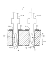
続いて、本実施形態のプレスフィット端子10の作用について説明する。以下では、隣接するスルーホール22間のピッチPが狭ピッチとされた回路基板20(図4参照)のスルーホール22にプレスフィット端子10を挿入する場合を例示する。このスルーホール22の内周面には、図4に示すように、メッキ処理等が施された接点部を有する導電路24が設けられている。
プレスフィット端子10を案内部12側から回路基板20のスルーホール22に挿入方向に沿って挿入すると、各対向部14の第1接触部14A及び第2接触部14Bがスルーホール22の開口端に突き当たって押圧される。そして、プレスフィット端子をスルーホール22にさらに挿入することで、各対向部14の第1接触部14A及び第2接触部14Bが弾性変形しながらスルーホール22内に進入し、スルーホール22の内周面(導電路24の接点部)に弾性的に接触する。これにより、プレスフィット端子10が回路基板20の導電路24と電気的に接続される。
ここで、隣接するスルーホール22の各々に挿入されたプレスフィット端子10を当該プレスフィット端子10の挿入方向と直交する断面で視ると、図5に示すように、隣接するスルーホール22の間では、一方のプレスフィット端子10の第1接触部14Aが接触した部分と他方のプレスフィット端子10の第2接触部14Bが接触した部分が隣り合う。従って、隣接するスルーホール22の間では、第1接触部14Aが接触した部分と第2接触部14Bが接触した部分とが互い違い状に配置された状態となる。なお、第1接触部14Aの曲率半径と第2接触部14Bの曲率半径は異なるので、両接触部14A,14Bがスルーホール22の内周面に接触した状態では、両対向部14がわずかに歪んだ形となる。
また、上述したように、第1接触部14A及び第2接触部14Bがスルーホール22の内周面に接触した際、接圧によって回路基板20が受けるダメージは第2接触部14Bからよりも第1接触部14Aからの方が小さい。このため、図5に示すように、回路基板20のうち第1接触部14Aから加わる接圧によりダメージを受ける領域(図5において符号D2で示す部分。以下、「第2の基板ダメージ部」と称する)は、第2接触部14Bから加わる接圧によりダメージを受ける領域(図5において符号D1で示す部分。以下、「第1の基板ダメージ部」と称する)よりも小さい。
このため、隣接するスルーホール22の間で第1接触部14Aが接触した部分と第2接触部14Bが接触した部分とが互い違い状に配置されることで両接触部分が隣り合っても、図5に示すように、第1の基板ダメージ部D1と第2の基板ダメージ部D2との間は近接し難い。即ち、両基板ダメージ部D1,D2が近接することが抑制される。その結果、隣接するスルーホール22の間で回路基板20のダメージを受けた部分が近接することに起因する両スルーホール22間の絶縁性能の低下を抑制することができる。
一方、第1接触部14Aに比べて第2接触部14Bからスルーホール22の内周面に対して大きな接圧が加わることで、第2接触部14Bが当該内周面に対して良好に保持される。このため、スルーホール22内に保持されるプレスフィット端子10の保持力を低下させることなく、プレスフィット端子10とスルーホール22との間で十分な接続信頼性を確保することができる。以上のように本実施形態のプレスフィット端子10では、接続信頼性を確保しながら、絶縁性能の低下を抑制することができる。
なお、本実施形態のように隣接するスルーホール22の間が狭ピッチである場合、プレスフィット端子10の各対向部14を複雑な形状(例えば断面視多角形状)に加工することが難しい。これに対し、本実施形態のプレスフィット端子10の各対向部14は、上述したように、一部が面取りされることで曲率が設けられた断面視略長方形状であるため、各対向部14を形成するために複雑な加工を必要とすることがない。このため、隣接するスルーホール22の間のピッチの大小に拘わらず、本実施形態のプレスフィット端子10を実現することができる。
上記の実施形態の変形例を以下に列挙する。
(1)上記の実施形態では、プレスフィット端子の各対向部が断面視略長方形状とされた構成を例示したが、各対向部の断面視における形状は限定されない。
(1)上記の実施形態では、プレスフィット端子の各対向部が断面視略長方形状とされた構成を例示したが、各対向部の断面視における形状は限定されない。
(2)上記の実施形態では、プレスフィット端子における一対の対向部の間がスリットとされた構成を例示したが、一対の対向部の間の構成については限定されない。例えば一対の対向部の間に弾性部材が配されており、これにより、各対向部がスルーホールの内周面に弾性的に接触する構成とされていてもよい。
以上、実施形態について詳細に説明したが、これらは例示に過ぎず、請求の範囲を限定するものではない。請求の範囲に記載の技術には、以上に例示した具体例を様々に変形、変更したものが含まれる。
(実施例)
(実施例)
次に、本明細書で開示される技術を実施例によって具体的に説明する。実施例では、回路基板に設けられた隣接する2つのスルーホールに実施形態で例示したプレスフィット端子をそれぞれ挿入し、両端子間に直流電圧を印加した状態で高温高湿環境下に一定時間放置した後、隣接するスルーホールの間の絶縁性能を評価する耐久試験を行った。
この耐久試験では、恒温恒湿槽としてエスペック社製PSL-2SPHを使用し、JPCA規格に準拠して、温度条件を38~87℃、湿度条件を82~96%RH、両端子間に印加する電圧をDC5~100V、試験時間を最大1000hrとした。また、隣接するスルーホール間を狭ピッチとし、各プレスフィット端子における第1接触部の曲率半径(R1)に対する第2接触部の曲率半径(R2)の比率を20~100(%)の間で変化させて評価を行った。
絶縁性能の評価では、絶縁抵抗計として横河メータ&インスツルメンツ社製MY-40を使用し、隣接するスルーホールの間の絶縁抵抗の抵抗値が絶縁抵抗計で測定可能な最大値2000MΩより大きければ○判定とし、絶縁抵抗の抵抗値が2000MΩより小さければ×判定とした。その結果を図6の表に示す。
図6の表に示すように、第1接触部の曲率半径に対する第2接触部の曲率半径の比率が75%以下である場合、即ち、第2接触部の曲率半径を第1接触部の曲率半径で除した値が0.75以下である場合、○判定が得られた。この結果から、各プレスフィット端子について、隣接するスルーホールの間の絶縁性能の低下を効果的に抑制するための、第1接触部の曲率半径及び第2接触部の曲率半径の具体的な値を設定することができる。
1:基板用コネクタ
10:プレスフィット端子
14,114:対向部
14A:第1接触部
14B:第2接触部
20:回路基板
22,122:スルーホール
10:プレスフィット端子
14,114:対向部
14A:第1接触部
14B:第2接触部
20:回路基板
22,122:スルーホール
Claims (3)
- 基板に設けられたスルーホールに挿入方向に沿って挿入されることで該スルーホール内に保持されるプレスフィット端子であって、
前記スルーホールの内周面に弾性的に接触する第1接触部及び第2接触部を有し、
前記挿入方向と直交する断面の断面視において、前記第2接触部の曲率半径を前記第1接触部の曲率半径で除した値が0.75以下であるプレスフィット端子。 - 対向状に配された一対の対向部を有し、
前記第1接触部及び前記第2接触部は、前記一対の対向部の各々に設けられ、
前記挿入方向と直交する断面の断面視において、前記一対の対向部の間で前記第1接触部同士を結ぶ線分と前記第2接触部同士を結ぶ線分とが交差する、請求項1に記載のプレスフィット端子。 - 基板の端子挿通孔に接続される請求項1または請求項2に記載のプレスフィット端子と、
前記プレスフィット端子を複数収容可能なハウジングと、
を有する基板用コネクタ。
Priority Applications (3)
| Application Number | Priority Date | Filing Date | Title |
|---|---|---|---|
| DE112016001768.5T DE112016001768B4 (de) | 2015-04-14 | 2016-03-24 | Leiterplattensteckverbinder |
| CN201680021099.0A CN107431296B (zh) | 2015-04-14 | 2016-03-24 | 基板用连接器 |
| US15/565,743 US10014606B2 (en) | 2015-04-14 | 2016-03-24 | Press-fit terminal and board connector |
Applications Claiming Priority (2)
| Application Number | Priority Date | Filing Date | Title |
|---|---|---|---|
| JP2015-082434 | 2015-04-14 | ||
| JP2015082434A JP6447333B2 (ja) | 2015-04-14 | 2015-04-14 | 基板用コネクタ |
Publications (1)
| Publication Number | Publication Date |
|---|---|
| WO2016167095A1 true WO2016167095A1 (ja) | 2016-10-20 |
Family
ID=57126536
Family Applications (1)
| Application Number | Title | Priority Date | Filing Date |
|---|---|---|---|
| PCT/JP2016/059325 Ceased WO2016167095A1 (ja) | 2015-04-14 | 2016-03-24 | プレスフィット端子及び基板用コネクタ |
Country Status (5)
| Country | Link |
|---|---|
| US (1) | US10014606B2 (ja) |
| JP (1) | JP6447333B2 (ja) |
| CN (1) | CN107431296B (ja) |
| DE (1) | DE112016001768B4 (ja) |
| WO (1) | WO2016167095A1 (ja) |
Families Citing this family (4)
| Publication number | Priority date | Publication date | Assignee | Title |
|---|---|---|---|---|
| JP6953919B2 (ja) * | 2017-09-04 | 2021-10-27 | 株式会社デンソー | プレスフィット端子及び電子装置 |
| CN107742787A (zh) * | 2017-10-31 | 2018-02-27 | 业成科技(成都)有限公司 | 连接电子元件与电路板的连接模组 |
| JP7205714B2 (ja) * | 2018-12-28 | 2023-01-17 | 株式会社オートネットワーク技術研究所 | プレスフィット端子 |
| JP7084331B2 (ja) | 2019-01-29 | 2022-06-14 | 京セラ株式会社 | プレスフィット端子 |
Citations (3)
| Publication number | Priority date | Publication date | Assignee | Title |
|---|---|---|---|---|
| JPS6440175U (ja) * | 1987-09-04 | 1989-03-09 | ||
| JP2001148261A (ja) * | 1999-11-22 | 2001-05-29 | Japan Aviation Electronics Industry Ltd | 基板スルーホール接続用コンタクトおよびコネクタ |
| JP2007059106A (ja) * | 2005-08-23 | 2007-03-08 | Auto Network Gijutsu Kenkyusho:Kk | プレスフィット端子と基板の接続構造、及びプレスフィット端子の設計方法 |
Family Cites Families (16)
| Publication number | Priority date | Publication date | Assignee | Title |
|---|---|---|---|---|
| US4443053A (en) * | 1982-08-05 | 1984-04-17 | Altron Incorporated | Electrical contact |
| US4606589A (en) * | 1984-01-12 | 1986-08-19 | H & V Services | Compliant pin |
| JPH0431740Y2 (ja) * | 1986-09-26 | 1992-07-30 | ||
| JP2911043B2 (ja) | 1989-10-13 | 1999-06-23 | 住友スリーエム株式会社 | プレスフィットコンタクトピン |
| US5154621A (en) * | 1991-07-29 | 1992-10-13 | Zierick Manufacturing Corporation | Printed circuit board contact system |
| JP3250902B2 (ja) * | 1994-03-04 | 2002-01-28 | 富士通株式会社 | プレスフィットピン |
| JP2929176B2 (ja) * | 1996-09-20 | 1999-08-03 | モレックス インコーポレーテッド | プレスフィットピン |
| US6098281A (en) * | 1996-11-06 | 2000-08-08 | Weidmuller Interface Gmbh & Co. | Electrical pins and method for their insertion into apertures of a circuit board |
| JP2004127610A (ja) * | 2002-09-30 | 2004-04-22 | Fujitsu Ten Ltd | プレスフィット端子 |
| US6969261B2 (en) * | 2003-08-01 | 2005-11-29 | Hewlett-Packard Development Company, L.P. | Electrical connector |
| JP2005353567A (ja) | 2004-05-10 | 2005-12-22 | Yazaki Corp | プレスフィット端子およびそれを用いた回路基板モジュール |
| WO2008038331A1 (en) | 2006-09-25 | 2008-04-03 | Autonetworks Technologies, Ltd. | Press fit terminal |
| US20080166928A1 (en) * | 2007-01-10 | 2008-07-10 | Liang Tang | Compliant pin |
| JP5019174B2 (ja) * | 2007-08-03 | 2012-09-05 | 山一電機株式会社 | 高速伝送用コネクタ |
| JP2013131364A (ja) * | 2011-12-21 | 2013-07-04 | Sumitomo Wiring Syst Ltd | 端子金具及び端子金具の接続構造 |
| DE102013004919B4 (de) | 2013-03-22 | 2015-09-03 | H & B Electronic Gmbh & Co. Kg | Leiterplattensteckverbinder |
-
2015
- 2015-04-14 JP JP2015082434A patent/JP6447333B2/ja not_active Expired - Fee Related
-
2016
- 2016-03-24 WO PCT/JP2016/059325 patent/WO2016167095A1/ja not_active Ceased
- 2016-03-24 DE DE112016001768.5T patent/DE112016001768B4/de not_active Expired - Fee Related
- 2016-03-24 CN CN201680021099.0A patent/CN107431296B/zh not_active Expired - Fee Related
- 2016-03-24 US US15/565,743 patent/US10014606B2/en active Active
Patent Citations (3)
| Publication number | Priority date | Publication date | Assignee | Title |
|---|---|---|---|---|
| JPS6440175U (ja) * | 1987-09-04 | 1989-03-09 | ||
| JP2001148261A (ja) * | 1999-11-22 | 2001-05-29 | Japan Aviation Electronics Industry Ltd | 基板スルーホール接続用コンタクトおよびコネクタ |
| JP2007059106A (ja) * | 2005-08-23 | 2007-03-08 | Auto Network Gijutsu Kenkyusho:Kk | プレスフィット端子と基板の接続構造、及びプレスフィット端子の設計方法 |
Also Published As
| Publication number | Publication date |
|---|---|
| US10014606B2 (en) | 2018-07-03 |
| US20180083377A1 (en) | 2018-03-22 |
| DE112016001768B4 (de) | 2021-08-05 |
| CN107431296B (zh) | 2019-06-18 |
| DE112016001768T5 (de) | 2018-01-18 |
| JP6447333B2 (ja) | 2019-01-09 |
| JP2016201329A (ja) | 2016-12-01 |
| CN107431296A (zh) | 2017-12-01 |
Similar Documents
| Publication | Publication Date | Title |
|---|---|---|
| US7048594B2 (en) | Terminal | |
| JP5748378B2 (ja) | コネクタ及びそれに用いるコンタクト | |
| JP2012129109A (ja) | コネクタ及びそれに用いるコンタクト | |
| US20130084759A1 (en) | Contact and electrical connector | |
| JP6447333B2 (ja) | 基板用コネクタ | |
| CN106663886A (zh) | 带端子印制电路板 | |
| JP2006228669A (ja) | 電気コネクタの接続端子 | |
| CN108429027A (zh) | 压配合端子 | |
| JP5008582B2 (ja) | コンタクトプローブ | |
| US20130084758A1 (en) | Contact and electrical connector | |
| JP5094343B2 (ja) | コネクタ及び該コネクタの接続部の検査方法 | |
| CN113631932A (zh) | 探针、检查工具和检查单元 | |
| TWI396339B (zh) | 連接器 | |
| JP6155820B2 (ja) | プレスフィット用コネクタ端子 | |
| JP2009152432A (ja) | 電子部品モジュール | |
| US9859637B2 (en) | Electrical connector | |
| JP2020072015A (ja) | プレスフィット端子及び電気部品 | |
| JP5816065B2 (ja) | 接続体 | |
| JP2021114399A (ja) | 端子 | |
| WO2021106546A1 (ja) | プレスフィット端子、プレスフィット端子付基板及び機器 | |
| JP4638803B2 (ja) | ミニアチュア差込接続部のための、一部分から成る多脚式のコンタクトばね | |
| JPH08124617A (ja) | 電気コネクタ端子及び電気コネクタ | |
| WO2023219006A1 (ja) | プレスフィット端子及び基板用コネクタ | |
| JP3214081U (ja) | 情報通信用電気端子板 | |
| JP2007165217A (ja) | 同軸コネクタ |
Legal Events
| Date | Code | Title | Description |
|---|---|---|---|
| 121 | Ep: the epo has been informed by wipo that ep was designated in this application |
Ref document number: 16779886 Country of ref document: EP Kind code of ref document: A1 |
|
| WWE | Wipo information: entry into national phase |
Ref document number: 15565743 Country of ref document: US |
|
| WWE | Wipo information: entry into national phase |
Ref document number: 112016001768 Country of ref document: DE |
|
| 122 | Ep: pct application non-entry in european phase |
Ref document number: 16779886 Country of ref document: EP Kind code of ref document: A1 |