WO2016167089A1 - 回路基板 - Google Patents
回路基板 Download PDFInfo
- Publication number
- WO2016167089A1 WO2016167089A1 PCT/JP2016/059098 JP2016059098W WO2016167089A1 WO 2016167089 A1 WO2016167089 A1 WO 2016167089A1 JP 2016059098 W JP2016059098 W JP 2016059098W WO 2016167089 A1 WO2016167089 A1 WO 2016167089A1
- Authority
- WO
- WIPO (PCT)
- Prior art keywords
- chip
- terminal capacitor
- pair
- wiring pattern
- circuit board
- Prior art date
- Legal status (The legal status is an assumption and is not a legal conclusion. Google has not performed a legal analysis and makes no representation as to the accuracy of the status listed.)
- Ceased
Links
Images




Classifications
-
- H—ELECTRICITY
- H05—ELECTRIC TECHNIQUES NOT OTHERWISE PROVIDED FOR
- H05K—PRINTED CIRCUITS; CASINGS OR CONSTRUCTIONAL DETAILS OF ELECTRIC APPARATUS; MANUFACTURE OF ASSEMBLAGES OF ELECTRICAL COMPONENTS
- H05K1/00—Printed circuits
- H05K1/02—Details
-
- H—ELECTRICITY
- H05—ELECTRIC TECHNIQUES NOT OTHERWISE PROVIDED FOR
- H05K—PRINTED CIRCUITS; CASINGS OR CONSTRUCTIONAL DETAILS OF ELECTRIC APPARATUS; MANUFACTURE OF ASSEMBLAGES OF ELECTRICAL COMPONENTS
- H05K1/00—Printed circuits
- H05K1/18—Printed circuits structurally associated with non-printed electric components
-
- H—ELECTRICITY
- H05—ELECTRIC TECHNIQUES NOT OTHERWISE PROVIDED FOR
- H05K—PRINTED CIRCUITS; CASINGS OR CONSTRUCTIONAL DETAILS OF ELECTRIC APPARATUS; MANUFACTURE OF ASSEMBLAGES OF ELECTRICAL COMPONENTS
- H05K3/00—Apparatus or processes for manufacturing printed circuits
- H05K3/46—Manufacturing multilayer circuits
Definitions
- the present invention relates to a circuit board on which a chip three-terminal capacitor is mounted.
- Patent Document 1 discloses a circuit board on which a chip three-terminal capacitor in which equivalent series inductance (residual inductance) is reduced is mounted.
- FIG. 11A shows the internal structure of the chip three-terminal capacitor 100.
- the chip three-terminal capacitor 100 has a substantially rectangular parallelepiped outer shape.
- a plurality of through internal electrodes 101 and a plurality of ground internal electrodes 102 are alternately stacked.
- the through internal electrode 101 and the ground internal electrode 102 serve as a pair of capacitors.
- the through internal electrode 101 reaches the other end from one end in the longitudinal direction of the chip three-terminal capacitor 100.
- Each of the through internal electrodes 101 is connected to one external terminal 103 at one end and is connected to the other external terminal 104 at the other end.
- Each of the ground internal electrodes 102 has a substantially cross-shaped planar shape, and is exposed on a pair of side surfaces orthogonal to the width direction.
- the ground internal electrode 102 is connected to one ground terminal 105 at a portion exposed on one side surface, and is connected to the other ground terminal 106 at a portion exposed on the other side surface.
- the chip three-terminal capacitor 100 actually has four terminals. Since a lead-type three-terminal capacitor intended to reduce the equivalent series inductance has three terminals, even a chip capacitor is conventionally expressed as “three terminals”.
- the through via 107 penetrates the chip three-terminal capacitor 100 in the thickness direction.
- the through via 107 is electrically connected to the through internal electrode 101 at an intersection with the through internal electrode 101, and passes through the opening 25 provided in the ground internal electrode 102. Insulated.
- FIG. 11B shows a perspective view of a conductor portion of a circuit board on which the chip three-terminal capacitor 100 is mounted.
- Power supply wiring patterns 110 and 111 and ground wiring patterns 120 and 121 are arranged on the surface of the circuit board.
- the power supply wiring patterns 110 and 111 are arranged along one virtual straight line and are separated from each other.
- the power supply wiring pattern 111 is connected to the power supply terminal of the integrated circuit element 130 mounted on the circuit board.
- the ground wiring patterns 120 and 121 are arranged along one virtual straight line that is orthogonal to the virtual straight line along which the power supply wiring patterns 110 and 111 extend. Has been.
- a power plane 115 and a ground plane 125 are arranged in different layers inside the circuit board.
- the power supply wiring patterns 110 and 111 are connected to the power supply plane 115 through vias 116 and 118, respectively.
- the ground wiring patterns 120 and 121 are connected to the ground plane 125 through vias 122 and 123, respectively.
- a via 117 is disposed at a location where the power supply wiring patterns 110 and 111 are separated. The via 117 extends from the power supply plane 115 toward the surface.
- the chip three-terminal capacitor 100 is surface-mounted on the circuit board.
- the external terminals 103 and 104 of the chip three-terminal capacitor 100 are connected to the power wiring patterns 110 and 111, the ground terminals 105 and 106 are connected to the ground wiring patterns 120 and 121, respectively, and the through via 107 is connected to the via 117. Is done.
- the equivalent series inductance formed between the power supply wiring pattern and the ground layer can be reduced.
- the chip three-terminal capacitor described in Patent Document 1 has a through via extending in the thickness direction.
- a technique for reducing the equivalent series inductance by using a general chip three-terminal capacitor having no through via is desired.
- An object of the present invention is to provide a circuit board capable of reducing an equivalent series inductance using a general chip three-terminal capacitor.
- a circuit board provides: A wiring board having a first conductor pattern and a second conductor pattern disposed therein; A wiring pattern provided on the surface of the wiring board; A pair of conductive lands arranged on the surface of the wiring board so as to sandwich the wiring pattern; and A chip three-terminal capacitor mounted on the wiring board; A conductive first via electrically connecting the wiring pattern to the first conductor pattern; A second via electrically connecting each of the pair of lands to the second conductor pattern;
- the chip three-terminal capacitor has a planar shape in which the dimension in the longitudinal direction is longer than the dimension in the width direction, and a pair of electrodes constituting the capacitance is provided therein, and one of the pair of electrodes Connected first terminals are provided at both ends in the longitudinal direction of the chip three-terminal capacitor, and second terminals connected to the other of the pair of electrodes are provided at both ends in the width direction.
- the chip three-terminal capacitor is mounted on the wiring board so that the longitudinal direction thereof is along the wiring pattern, the pair of first terminals are connected to the wiring pattern, and the pair of second terminals are , Each connected to a pair of lands, The first via is disposed at a position overlapping the chip three-terminal capacitor.
- the chip three-terminal capacitor is mounted on the wiring board in such a manner that its longitudinal direction is along the wiring pattern, the wiring pattern is not divided immediately below the chip three-terminal capacitor. For this reason, the equivalent series inductance of the wiring pattern can be reduced.
- the distance from the virtual straight line connecting the centers of the pair of second vias to the center of the first via is not more than 1 ⁇ 2 of the longitudinal dimension of the chip three-terminal capacitor.
- the first via and the second via are arranged so that an imaginary straight line connecting the centers of the pair of second vias is in contact with the first via.
- the equivalent series inductance of the current path including the first via and the second via can be further reduced.
- the circuit board according to the fourth aspect of the present invention in addition to the configuration of the circuit board according to the first to third aspects,
- the wiring pattern and the first conductor pattern are connected, overlap with the chip three-terminal capacitor, and have at least one third via disposed at a position different from the first via.
- the equivalent series inductance of the current path connecting the wiring pattern and the first conductor pattern can be reduced.
- the pair of second vias are disposed inside the chip three-terminal capacitor in plan view.
- the equivalent series inductance of the current path including the first via and the second via can be further reduced.
- the wiring pattern is narrower at the portion sandwiched between the pair of lands than the portion overlapping the end portion in the longitudinal direction of the chip three-terminal capacitor, and the first portion at the narrowed portion. Vias are arranged.
- the equivalent series inductance of the wiring pattern can be reduced compared to a configuration in which the entire wiring pattern is thin.
- the chip three-terminal capacitor is mounted on the wiring board in such a manner that its longitudinal direction is along the wiring pattern, the wiring pattern is not divided immediately below the chip three-terminal capacitor. For this reason, the equivalent series inductance of the wiring pattern can be reduced.
- FIG. 1 is a perspective view showing a structure of a conductor portion of a circuit board according to the first embodiment.
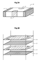
- 2A is a perspective view of a chip three-terminal capacitor mounted on the circuit board according to the first embodiment
- FIG. 2B is a perspective view showing an internal structure of the chip three-terminal capacitor.
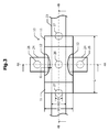
- FIG. 3 is a plan view of the chip three-terminal capacitor and the wiring board.
- 4A and 4B are cross-sectional views taken along one-dot chain lines 4A-4A and 4B-4B in FIG. 3, respectively.
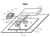
- FIG. 5 is a perspective view showing a structure of a conductor portion of a circuit board according to a comparative example.
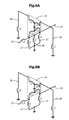
- 6A is an equivalent circuit diagram of a part of the circuit board according to the first embodiment
- FIG. 6B is an equivalent circuit diagram of a part of the circuit board according to the comparative example shown in FIG.
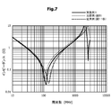
- FIG. 7 is a graph showing a simulation result of impedance by the electromagnetic field simulator.
- 8A, 8B, and 8C show a chip three-terminal capacitor mounted on a circuit board according to Example 2, Example 3, and Example 4, respectively, and a circuit board wiring pattern, land, first via
- FIG. 6 is a plan view of a second via.
- FIG. 9 is a perspective view of a conductor portion of a circuit board according to the fifth embodiment.
- FIG. 10 is a plan view of the chip three-terminal capacitor mounted on the circuit board according to the sixth embodiment and the wiring patterns and lands provided on the surface of the circuit board.
- FIG. 11A is a perspective view showing an internal structure of a conventional chip three-terminal capacitor
- FIG. 11B is a perspective view of a conductor portion of a circuit board on which the conventional chip three-terminal capacitor is mounted.
- circuit substrate a dielectric substrate on which a conductor pattern for connecting components is formed
- circuit substrate a substrate composed of the wiring substrate and components mounted thereon
- FIG. 1 shows a perspective view of a conductor portion of a circuit board according to an embodiment.
- the dielectric portion is not shown.
- the chip three-terminal capacitor 10 and the integrated circuit element 30 are mounted on the surface of the circuit board.
- a first conductor pattern 21 is disposed inside the circuit board.
- the second conductor pattern 22 is disposed at a position deeper than the first conductor pattern 21.
- a wiring pattern 23 extending in a straight line is provided on the surface of the wiring board.
- the wiring pattern 23 is connected to the integrated circuit element 30 at one end thereof.
- a pair of conductive lands 24 are provided on the surface of the wiring board so as to sandwich the wiring pattern 23.
- a conductive first via 26 is disposed at a location sandwiched between the pair of lands 24.
- the first via 26 electrically connects the wiring pattern 23 to the first conductor pattern 21.
- the pair of lands 24 are electrically connected to the second conductor pattern 22 by the respective conductive second vias 28.
- the second via 28 is insulated from the first conductor pattern 21 by passing through the opening 25 provided in the first conductor pattern 21.
- the wiring pattern 23 is electrically connected to the first conductor pattern 21 by at least one third via 27 disposed at a position different from the first via 26. In the example shown in FIG. 1, two third vias 27 are arranged so as to sandwich the first via 26.
- the chip three-terminal capacitor 10 has a planar shape in which the dimension in the longitudinal direction is longer than the dimension in the width direction.
- a pair of electrodes is provided inside the chip three-terminal capacitor 10, and a capacitance is constituted by the pair of electrodes.
- First terminals 11 are provided at both ends of the chip three-terminal capacitor 10 in the longitudinal direction, and a pair of second terminals 12 are provided at both ends in the width direction.
- One of the pair of electrodes constituting the capacitance is connected to the first terminal 11, and the other is connected to the second terminal 12.
- the chip three-terminal capacitor 10 is surface-mounted on the wiring board with the longitudinal direction thereof along the wiring pattern 23.
- a pair of first terminals 11 are connected to one wiring pattern 23, and a pair of second terminals 12 are connected to a pair of lands 24, respectively.
- the first via 26 is disposed at a position overlapping the chip three-terminal capacitor 10.
- the second conductor pattern 22 is dropped to the ground potential, and a power supply voltage is applied to the first conductor pattern 21.
- the wiring pattern 23 is connected to the power supply terminal of the integrated circuit element 30.
- the chip three-terminal capacitor 10 functions as a bypass capacitor (decoupling capacitor) inserted between the ground wiring and the power supply wiring.
- FIG. 2A shows a perspective view of the chip three-terminal capacitor 10.
- the chip three-terminal capacitor 10 has a substantially rectangular parallelepiped outer shape.
- First terminals 11 are provided at both ends of the chip three-terminal capacitor 10 in the longitudinal direction.
- the first terminal 11 covers the entire region of the pair of end surfaces orthogonal to the longitudinal direction, and wraps around the upper surface, the bottom surface, and the region in the vicinity of the end portions of the side surfaces.
- the second terminals 12 are provided on a pair of side surfaces orthogonal to the width direction.
- the second terminal 12 is disposed substantially in the center with respect to the longitudinal direction of the side surface. Furthermore, the second terminal 12 wraps around from the edge of the top surface and the bottom surface to a part of the region inward.
- FIG. 2B shows the internal structure of the chip three-terminal capacitor 10.
- a plurality of plate-like first electrodes 13 and a plurality of second electrodes 14 are alternately stacked.
- the first electrode 13 and the second electrode 14 that are adjacent to each other are insulated from each other by a dielectric layer.
- the first electrode 13 and the second electrode 14 constitute a capacitance.
- the first electrode 13 extends from one end face in the longitudinal direction of the chip three-terminal capacitor 10 to the other end face, and is connected to the first terminal 11.
- the second electrode 14 is exposed on a pair of side surfaces orthogonal to the width direction, and is connected by the second terminal 12.
- a power supply voltage is applied to the first electrode 13 from the first conductor pattern 21 via the first via 26, the third via 27, and the wiring pattern 23 (FIG. 1).
- the second electrode 14 is dropped to the ground potential via the land 24, the second via 28, and the second conductor pattern 22 (FIG. 1).
- FIG. 3 shows a plan view of the chip three-terminal capacitor 10 and the wiring board.
- the chip three-terminal capacitor 10 is mounted on the wiring board such that its longitudinal direction follows the wiring pattern 23.
- the wiring pattern 23 continues immediately below the chip three-terminal capacitor 10 from one end in the longitudinal direction to the other end.
- a pair of lands 24 sandwich the wiring pattern 23.
- the pair of lands 24 are connected to the pair of second terminals 12, respectively.
- a second via 28 is disposed at a position overlapping each land 24.
- a first via 26 and at least one third via 27 are disposed at a position overlapping the wiring pattern 23.
- the first via 26 is disposed so as to contact a virtual straight line connecting the centers of the pair of second vias 28.
- the length L of the chip three-terminal capacitor 10 is 1.6 mm, and the width W1 is 0.8 mm.
- the width W2 of the wiring pattern 23 is 0.4 mm, and the diameter D1 of the first via 26, the second via 28, and the third via 27 is 0.3 mm.
- the interval G between the wiring pattern 23 and the land 24 is set to the minimum clearance of the pattern design rule.
- the minimum clearance is, for example, in the range of 0.1 mm to 0.2 mm.
- FIG. 4A is a cross-sectional view taken along one-dot chain line 4A-4A in FIG.
- a wiring pattern 23 is provided on the surface of the wiring substrate 20 made of a dielectric. Lands 24 are respectively provided on both sides of the wiring pattern 23.
- a first conductor pattern 21 is disposed inside the wiring board 20, and a second conductor pattern 22 is disposed at a deeper position.
- the first via 26 connects the wiring pattern 23 to the first conductor pattern 21.
- a pair of second vias 28 respectively connect the pair of lands 24 to the second conductor pattern 22.
- the second via 28 vertically penetrates the opening 25 provided in the first conductor pattern 21.
- the chip three-terminal capacitor 10 is surface-mounted on the wiring board 20.
- the pair of second terminals 12 are connected to the pair of lands 24, respectively.
- a plurality of first electrodes 13 and a plurality of second electrodes 14 are alternately stacked.
- Each of the second electrodes 14 is connected to the second terminal 12 at both ends thereof.
- FIG. 4B shows a cross-sectional view taken along one-dot chain line 4B-4B in FIG.
- a wiring pattern 23 is provided on the surface of the wiring board 20.
- the first terminal 11 of the chip three-terminal capacitor 10 is connected to the wiring pattern 23.
- the wiring pattern 23 passes directly below the chip three-terminal capacitor 10 in the longitudinal direction of the chip three-terminal capacitor 10.
- a first electrode 13 in the chip three-terminal capacitor 10 is connected to the first terminal 11.
- the wiring pattern 23 is connected to the first conductor pattern 21 via the first via 26 and at least one third via 27.
- FIG. 5 shows a perspective view of a conductor portion of a circuit board according to a comparative example.
- the wiring pattern 23 passes directly below the chip three-terminal capacitor 10 in the longitudinal direction.
- the wiring pattern 23 is divided in the length direction immediately below the chip three-terminal capacitor 10. One part of the divided wiring pattern 23 is connected to one first terminal 11 of the chip three-terminal capacitor 10, and the other part is connected to the other first terminal 11.
- the first via 26 (FIG. 1) is not provided.
- FIG. 6A shows an equivalent circuit diagram of a part of the circuit board according to the first embodiment.
- the chip three-terminal capacitor 10 itself has an equivalent series inductance L1 inserted in series with the capacitance.
- the first via 26 has an equivalent series inductance L2, and each of the pair of second vias 28 has an equivalent series inductance L3.
- the wiring pattern 23 has an equivalent series inductance L4.
- Each of the third vias 27 has an equivalent series inductance L5.
- the equivalent series inductances L2, L3, L4, and L5 degrade the electrical characteristics of the electric circuit formed on the circuit board.
- FIG. 6B shows an equivalent circuit diagram of a part of the circuit board according to the comparative example shown in FIG.
- the wiring pattern 23 is divided immediately below the chip three-terminal capacitor 10. Since the first via 26 is not disposed, the equivalent series inductance L2 (FIG. 6A) does not exist.
- the electrical signal propagating through the wiring pattern 23 is detoured to the equivalent series inductance L5 possessed by the third via 27 and the equivalent series inductance L1 possessed by the chip three terminal capacitor 10 at the parting position immediately below the chip three terminal capacitor 10. For this reason, the electrical signal propagating through the wiring pattern 23 passes through the bypass path inductance, that is, the equivalent series inductance L1 or L5, in addition to the equivalent series inductance L4.
- the power supply wiring patterns 110 and 111 are separated from each other immediately below the chip three-terminal capacitor 100. For this reason, as in the comparative example shown in FIG. 5, the electrical signal propagating toward the integrated circuit element 130 via the power supply wiring patterns 110 to 111 passes through the bypass path inductance.
- Example 1 As shown in FIG. 6A, the wiring pattern 23 (FIG. 1) is not divided immediately below the chip three-terminal capacitor 10. An electric signal that propagates through the wiring pattern 23 without detouring does not pass through the equivalent series inductances L1 and L5. For this reason, stable power supply to the integrated circuit element 30 becomes possible.
- FIG. 11A and FIG. 11B a chip three-terminal capacitor 100 having a special structure provided with a through via 107 must be used.
- a general one without the through via 107 FIG. 11A
- the conventional example shown in FIGS. 11A and 11B is disadvantageous in terms of downsizing the chip three-terminal capacitor 100 because the through via 107 is incorporated in the chip three-terminal capacitor 100. Furthermore, since the through via 107 is disposed, the area of the portion where the through internal electrode 101 and the ground internal electrode 102 (FIG. 11A) face each other is reduced. This is also disadvantageous in increasing the capacitance. On the other hand, since the through via 107 is not disposed in the chip three-terminal capacitor 10 mounted on the circuit board according to the first embodiment, it is advantageous in terms of downsizing and increasing the capacity of the chip three-terminal capacitor 10.
- the first via 26 and the second via 26 so that the straight line connecting the centers of the second vias 28 is in contact with the first via 26.
- a via 28 is disposed.
- the distance between the first via 26 and the second via 28 is narrowed.
- the magnetic flux caused by the current flowing through the first via 26 and the magnetic flux caused by the current flowing in the opposite direction through the second via 28 efficiently cancel each other.
- the combined inductance of the equivalent series inductances L2 and L3 is reduced. Since the deterioration of the performance of the bypass capacitor due to the equivalent series inductances L1, L2, and L3 is suppressed, more stable power supply can be performed.
- Fig. 7 shows the simulation results of impedance using an electromagnetic simulator.
- the simulation result shows the impedance when the power supply side is viewed from the integrated circuit element 30 shown in FIG.
- the simulation was performed under the condition that the wiring pattern 23 was terminated at 50 ⁇ .
- the horizontal axis in FIG. 7 represents the frequency in the unit “MHz”, and the vertical axis represents the impedance in the unit “ ⁇ ”.
- the thick solid line, thin broken line, and thick broken line in the graph of FIG. 7 indicate the impedance of the circuit board according to the first embodiment shown in FIG. 1, the comparative example shown in FIG. 5, and the conventional example shown in FIG. 11B, respectively.
- the dimensions of common components are the same in any circuit board to be simulated.
- the effect of the equivalent series inductance hardly appears, so the impedance decreases as the frequency increases.
- the resonance frequency of the equivalent series inductance and the capacitance is exceeded, the influence of the equivalent series inductance increases, and the impedance increases as the frequency increases.
- the resonance frequency of the circuit board according to Example 1 is higher than the resonance frequency of the circuit board according to the comparative example shown in FIG. This is because the equivalent series inductance is reduced. Further, in the range higher than the resonance frequency, the impedance of the circuit board according to Example 1 is lower than the impedance of the circuit board according to the comparative example shown in FIG. It was confirmed by simulation that the equivalent series inductance is reduced by employing the structure of Example 1.
- the resonance frequency of the circuit board of the conventional example is higher. Further, in the range higher than the resonance frequency, the impedance of the circuit board of the conventional example is lower.
- a chip three-terminal capacitor 100 having a special structure having the through via 107 shown in FIG. 11A must be used for the circuit board according to the conventional example.
- the circuit board according to the first embodiment can use the chip three-terminal capacitor 10 (FIGS. 2A and 2B) having a general structure.
- the circuit board according to the first embodiment is superior to the conventional circuit board shown in FIG. 11B in that a general chip three-terminal capacitor can be used.
- Embodiments 2 to 4 will be described with reference to FIGS. 8A to 8C.
- differences from the first embodiment will be described, and description of common configurations will be omitted.
- FIG. 8A shows a plan view of the chip three-terminal capacitor 10 mounted on the circuit board according to the second embodiment, the wiring pattern 23 of the circuit board, the land 24, the first via 26, and the second via 28.
- FIG. 8A In order to reduce the equivalent series inductance, it is preferable to bring the first via 26 and the second via 28 close to each other. However, when it is difficult to arrange the first via 26 so that the first via 26 is in contact with a straight line passing through the centers of the two second vias 28 in relation to other conductor patterns. There is also.
- the first via 26 is arranged at a position deviating from a straight line passing through the centers of the two second vias 28.
- the first via 26 is arranged at a position overlapping the chip three-terminal capacitor 10. Since the wiring pattern 23 is continuous from one end portion in the longitudinal direction of the chip three-terminal capacitor 10 to the other end portion, the arrangement of the first vias 26 is provided as compared with the case where the wiring pattern 23 is divided. High degree of freedom.
- the distance D2 from the straight line passing through the centers of the two second vias 28 to the center of the first via 26 is set to 1 / of the length L of the chip three-terminal capacitor 10. More preferably, it is 4 or less.
- FIG. 8B shows a plan view of the chip three-terminal capacitor 10 mounted on the circuit board according to the third embodiment, and the wiring pattern 23, land 24, first via 26, and second via 28 of the circuit board.
- the second via 28 is disposed inside the chip three-terminal capacitor 10 in plan view.
- the insertion depth D3 of the land 24 from the edge to the inside of the chip three-terminal capacitor 10 is set to at least the diameter D1 of the second via 28. Must be on the same level as
- the width W3 In order to set the insertion depth D3 to be at least as large as the diameter D1 of the second via 28 and to set the distance G between the wiring pattern 23 and the land 24 to the minimum clearance based on the pattern design rule, In some cases, the width W3 must be narrower than the width W1 of the wiring pattern 23 (FIG. 3) of the first embodiment. As an example, when the width W1 of the chip three-terminal capacitor 10 is 0.8 mm, the width W3 of the wiring pattern 23, the diameter D1 of the first via 26, the second via 28, and the third via 27, and the insertion depth The lengths D3 are all 0.2 mm, and the gap G is 0.1 mm.
- the first via 26 and the second via 28 can be brought closer to each other. Thereby, the equivalent series inductance can be further reduced.
- FIG. 8C shows a plan view of the chip three-terminal capacitor 10 mounted on the circuit board according to the fourth embodiment, and the wiring pattern 23, land 24, first via 26, and second via 28 of the circuit board.
- the second via 28 is disposed inside the chip three-terminal capacitor 10 as in the third embodiment shown in FIG. 8B.
- the width W3 of the portion sandwiched between the lands 24 of the wiring pattern 23 overlaps both ends of the chip three-terminal capacitor 10 in the longitudinal direction. It is thinner than the width W2.
- the width W2 and the width W3 are 0.4 mm and 0.2 mm, respectively.
- the first via 26 is disposed in the narrowed portion of the wiring pattern 23.
- the portion other than the portion sandwiched between the lands 24 of the wiring pattern 23 can be made thick without being limited by the interval between the two lands 24.
- the equivalent series inductance L4 (FIG. 6A) of the wiring pattern 23 can be reduced.
- FIG. 9 is a perspective view of the conductor portion of the circuit board according to the fifth embodiment.
- the wiring pattern 23 (FIG. 1) along the longitudinal direction of the chip three-terminal capacitor 10 is connected to the integrated circuit element 30.
- one land 24 is connected to the integrated circuit element 30 through the wiring pattern 32.
- the wiring pattern 23 is connected to the second conductor pattern 22 via the first via 26 and the third via 27.
- the pair of lands 24 are connected to the first conductor pattern 21 via a pair of second vias 28, respectively.
- the wiring pattern 23 is dropped to the ground potential via the first via 26, the third via 27, and the second conductor pattern 22.
- a power supply voltage is applied to the land 24 from the first conductor pattern 21 through the second via 28.
- the first electrode 13 (FIG. 2B) connected to the first terminal 11 of the chip three-terminal capacitor 10 is dropped to the ground potential, and the second terminal A power supply voltage is applied to the second electrode 14 (FIG. 2B) connected to 12.
- the equivalent series inductance inserted in series with the chip three-terminal capacitor 10 can be reduced. As a result, stable power supply to the integrated circuit element 30 becomes possible.
- FIG. 10 is a plan view of the chip three-terminal capacitor 10 mounted on the circuit board according to the sixth embodiment, and the wiring pattern 23 and the land 24 provided on the surface of the circuit board.
- one second via 28 is connected to one land 24, and one first via 26 is arranged between the two lands 24.
- a plurality of second vias 28 are connected to one land 24, and a plurality of first vias 26 are arranged between the two lands 24.
- four second vias 28 are connected to one land 24, and four first vias 26 are arranged between the two lands 24.
- the equivalent series inductance can be reduced by increasing the number of the first vias 26 and the second vias 28.
- the equivalent series inductance can also be reduced by making the via thicker. However, if the first via 26 and the second via 28 are thicker than the other vias, the procedure for drilling the vias becomes complicated. By increasing the number of first vias 26 and second vias 28, the equivalent series inductance can be reduced while keeping the thicknesses of the first and second vias 26 and 28 the same as other vias. It becomes possible.
- a configuration is adopted in which one of the first electrode 13 and the second electrode 14 (FIG. 2B) of the chip three-terminal capacitor 10 is dropped to the ground potential and the power supply voltage is applied to the other.
- one of the first electrode 13 and the second electrode 14 may be dropped to the ground potential, and an electrical signal other than the power supply voltage may be applied to the other.
Landscapes
- Engineering & Computer Science (AREA)
- Microelectronics & Electronic Packaging (AREA)
- Manufacturing & Machinery (AREA)
- Production Of Multi-Layered Print Wiring Board (AREA)
- Structures For Mounting Electric Components On Printed Circuit Boards (AREA)
- Semiconductor Integrated Circuits (AREA)
Abstract
配線基板の内部に第1、第2の導体パターンが配置され、表面に配線パターンが設けられている。配線パターンを挟むように一対のランドが配置されている。第1のビアが、配線パターンを第1の導体パターンに接続し、第2のビアが、ランドを第2の導体パターンに接続する。チップ三端子コンデンサが、幅方向の寸法よりも長手方向の寸法の方が長い平面形状を有する。チップ三端子コンデンサの長手方向の両端に第1の端子が設けられており、幅方向の両端に第2の端子が設けられている。チップ三端子コンデンサは、その長手方向が配線パターンに沿う姿勢で配線基板に実装されており、第1の端子が配線パターンに接続され、第2の端子がランドに接続されている。第1のビアは、チップ三端子コンデンサと重なる位置に配置されている。
Description
本発明は、チップ三端子コンデンサを実装した回路基板に関する。
高周波特性に優れたバイパスコンデンサとして、チップ三端子コンデンサが利用されている。下記の特許文献1に、等価直列インダクタンス(残留インダクタンス)の低減を図ったチップ三端子コンデンサを実装した回路基板が開示されている。
図11A及び図11Bを参照して、特許文献1に開示されたチップ三端子コンデンサ及び回路基板について説明する。
図11Aに、チップ三端子コンデンサ100の内部構造を示す。チップ三端子コンデンサ100は、ほぼ直方体の外形を有する。複数の貫通内部電極101と複数のグランド内部電極102とが交互に積層されている。貫通内部電極101とグランド内部電極102とが、コンデンサの一対の電極として作用する。貫通内部電極101は、チップ三端子コンデンサ100の長手方向の一端から他端に達する。貫通内部電極101の各々が、一方の端部において一方の外部端子103に接続され、他方の端部において他方の外部端子104に接続されている。
グランド内部電極102の各々は、ほぼ十字状の平面形状を有し、幅方向と直交する一対の側面に露出している。グランド内部電極102は、一方の側面に露出した部分において一方のグランド端子105に接続され、他方の側面に露出した部分において他方のグランド端子106に接続されている。
チップ三端子コンデンサ100は、実際には4つの端子を有している。等価直列インダクタンスを低下させることを目的としたリードタイプの三端子コンデンサが3つの端子を有していたため、チップ化されたコンデンサにおいても、慣習的に「三端子」と表記される。
貫通ビア107がチップ三端子コンデンサ100を厚さ方向に貫通する。貫通ビア107は、貫通内部電極101との交差箇所において、貫通内部電極101に電気的に接続されており、グランド内部電極102に設けられた開口25を通過することによって、グランド内部電極102からは絶縁されている。
図11Bに、チップ三端子コンデンサ100が実装される回路基板の導体部分の斜視図を示す。回路基板の表面に、電源配線パターン110、111、及びグランド配線パターン120、121が配置されている。電源配線パターン110、111は、1本の仮想直線に沿って配置されており、相互に分断されている。電源配線パターン111は、回路基板に実装された集積回路素子130の電源端子に接続されている。グランド配線パターン120、121は、電源配線パターン110、111が沿う仮想直線と直交する1本の仮想直線に沿って配置されており、電源配線パターン110、111の分断箇所と同じ箇所で相互に分断されている。
回路基板の内部の相互に異なる層に、電源プレーン115及びグランドプレーン125が配置されている。電源配線パターン110、111が、それぞれビア116、118を介して電源プレーン115に接続されている。グランド配線パターン120、121が、それぞれビア122、123を介してグランドプレーン125に接続されている。電源配線パターン110と111との分断箇所に、ビア117が配置されている。ビア117は、電源プレーン115から表面に向かって延びる。
チップ三端子コンデンサ100が、回路基板に表面実装される。チップ三端子コンデンサ100の外部端子103、104が、それぞれ電源配線パターン110、111に接続され、グランド端子105、106が、それぞれグランド配線パターン120、121に接続され、貫通ビア107がビア117に接続される。
チップ三端子コンデンサ100内に貫通ビア107を設けることにより、電源配線パターンとグランド層との間に形成される等価直列インダクタンスを低減させることができる。
特許文献1に記載されたチップ三端子コンデンサは、その厚さ方向に延びる貫通ビアを有する。貫通ビアを持たない一般的なチップ三端子コンデンサを用いて、等価直列インダクタンスを低減させる技術が望まれている。
本発明の目的は、一般的なチップ三端子コンデンサを用いて、等価直列インダクタンスを低減させることが可能な回路基板を提供することである。
本発明の第1の観点による回路基板は、
内部に第1の導体パターンと第2の導体パターンとが配置された配線基板と、
前記配線基板の表面に設けられた配線パターンと、
前記配線基板の表面に、前記配線パターンを挟むように配置された一対の導電性のランドと、
前記配線基板に実装されたチップ三端子コンデンサと、
前記配線パターンを前記第1の導体パターンに電気的に接続する導電性の第1のビアと、
一対の前記ランドの各々を前記第2の導体パターンに電気的に接続する第2のビアと
を有し、
前記チップ三端子コンデンサは、幅方向の寸法よりも長手方向の寸法の方が長い平面形状を有し、静電容量を構成する一対の電極が内部に設けられ、一対の前記電極のうち一方に接続された第1の端子が前記チップ三端子コンデンサの前記長手方向の両端に設けられており、前記一対の前記電極のうち他方に接続された第2の端子が、幅方向の両端に設けられており、
前記チップ三端子コンデンサは、その長手方向が前記配線パターンに沿う姿勢で前記配線基板に実装されており、一対の前記第1の端子が前記配線パターンに接続され、一対の前記第2の端子が、それぞれ一対の前記ランドに接続されており、
前記第1のビアは、前記チップ三端子コンデンサと重なる位置に配置されている。
内部に第1の導体パターンと第2の導体パターンとが配置された配線基板と、
前記配線基板の表面に設けられた配線パターンと、
前記配線基板の表面に、前記配線パターンを挟むように配置された一対の導電性のランドと、
前記配線基板に実装されたチップ三端子コンデンサと、
前記配線パターンを前記第1の導体パターンに電気的に接続する導電性の第1のビアと、
一対の前記ランドの各々を前記第2の導体パターンに電気的に接続する第2のビアと
を有し、
前記チップ三端子コンデンサは、幅方向の寸法よりも長手方向の寸法の方が長い平面形状を有し、静電容量を構成する一対の電極が内部に設けられ、一対の前記電極のうち一方に接続された第1の端子が前記チップ三端子コンデンサの前記長手方向の両端に設けられており、前記一対の前記電極のうち他方に接続された第2の端子が、幅方向の両端に設けられており、
前記チップ三端子コンデンサは、その長手方向が前記配線パターンに沿う姿勢で前記配線基板に実装されており、一対の前記第1の端子が前記配線パターンに接続され、一対の前記第2の端子が、それぞれ一対の前記ランドに接続されており、
前記第1のビアは、前記チップ三端子コンデンサと重なる位置に配置されている。
チップ三端子コンデンサは、その長手方向が配線パターンに沿う姿勢で配線基板に実装されるため、配線パターンはチップ三端子コンデンサの直下で分断されない。このため、配線パターンの等価直列インダクタンスを小さくすることができる。
本発明の第2の観点による回路基板においては、第1の観点による回路基板の構成に加えて、
平面視において、一対の前記第2のビアの中心同士を結ぶ仮想直線から、前記第1のビアの中心までの距離が、前記チップ三端子コンデンサの前記長手方向の寸法の1/2以下である。
平面視において、一対の前記第2のビアの中心同士を結ぶ仮想直線から、前記第1のビアの中心までの距離が、前記チップ三端子コンデンサの前記長手方向の寸法の1/2以下である。
第1のビアと第2のビアとの間隔が狭くなるため、第1のビアを流れる電流による磁束と、第2のビアを逆方向に流れる磁束とが打ち消し合う。このため、第1のビア及び第2のビアを含む電流経路の等価直列インダクタンスを小さくすることができる。
本発明の第3の観点による回路基板においては、第1または第2の観点による回路基板の構成に加えて、
平面視において、一対の前記第2のビアの中心同士を結ぶ仮想直線が、前記第1のビアに接触するように、前記第1のビア及び前記第2のビアが配置されている。
平面視において、一対の前記第2のビアの中心同士を結ぶ仮想直線が、前記第1のビアに接触するように、前記第1のビア及び前記第2のビアが配置されている。
第1のビアと第2のビアとの間隔がより狭くなるため、第1のビア及び第2のビアを含む電流経路の等価直列インダクタンスを、より小さくすることができる。
本発明の第4の観点による回路基板は、第1乃至第3の観点による回路基板の構成に加えて、
前記配線パターンと前記第1の導体パターンとを接続し、前記チップ三端子コンデンサと重なり、前記第1のビアとは異なる位置に配置された少なくとも1つの第3のビアを有する。
前記配線パターンと前記第1の導体パターンとを接続し、前記チップ三端子コンデンサと重なり、前記第1のビアとは異なる位置に配置された少なくとも1つの第3のビアを有する。
配線パターンと第1の導体パターンとが第1のビア及び第3のビアで接続されるため、配線パターンと第1の導体パターンとを接続する電流経路の等価直列インダクタンスを小さくすることができる。
本発明の第5の観点による回路基板においては、第1乃至第4の観点による回路基板の構成に加えて、
一対の前記第2のビアが、平面視において、前記チップ三端子コンデンサの内側に配置されている。
一対の前記第2のビアが、平面視において、前記チップ三端子コンデンサの内側に配置されている。
第1のビアと第2のビアとの間隔がより狭くなるため、第1のビア及び第2のビアを含む電流経路の等価直列インダクタンスを、より小さくすることができる。
本発明の第6の観点による回路基板においては、第5の観点による回路基板の構成に加えて、
前記配線パターンが、一対の前記ランドに挟まれている部分において、前記チップ三端子コンデンサの前記長手方向の端部と重なっている部分よりも細くなっており、細くなっている部分に前記第1のビアが配置されている。
前記配線パターンが、一対の前記ランドに挟まれている部分において、前記チップ三端子コンデンサの前記長手方向の端部と重なっている部分よりも細くなっており、細くなっている部分に前記第1のビアが配置されている。
配線パターンの全体が細くなっている構成に比べて、配線パターンの等価直列インダクタンスを小さくすることができる。
チップ三端子コンデンサは、その長手方向が配線パターンに沿う姿勢で配線基板に実装されるため、配線パターンはチップ三端子コンデンサの直下で分断されない。このため、配線パターンの等価直列インダクタンスを小さくすることができる。
図1~図4Bを参照して、実施例1による回路基板の構成について説明する。本明細書において、部品間を接続するための導体パターンが形成された誘電体基板を「配線基板」といい、配線基板と、それに実装された部品とから構成される基板を「回路基板」という。
図1に、実施例による回路基板の導体部分の斜視図を示す。図1において、誘電体部分は示されていない。回路基板の表面に、チップ三端子コンデンサ10及び集積回路素子30が実装される。回路基板の内部に、第1の導体パターン21が配置されている。第1の導体パターン21より深い位置に、第2の導体パターン22が配置されている。
配線基板の表面に、直線状に延びる配線パターン23が設けられている。配線パターン23は、その一端において集積回路素子30に接続されている。配線パターン23を挟むように、配線基板の表面に、一対の導電性のランド24が設けられている。
一対のランド24に挟まれた箇所に、導電性の第1のビア26が配置されている。第1のビア26は、配線パターン23を第1の導体パターン21に電気的に接続する。一対のランド24が、それぞれ導電性の第2のビア28によって、第2の導体パターン22に電気的に接続されている。第2のビア28は、第1の導体パターン21に設けられた開口25を通過することにより、第1の導体パターン21から絶縁されている。配線パターン23は、第1のビア26とは異なる位置に配置された少なくとも1つの第3のビア27によって、第1の導体パターン21に電気的に接続されている。図1に示した例では、第1のビア26を挟むように2つの第3のビア27が配置されている。
チップ三端子コンデンサ10は、幅方向の寸法よりも長手方向の寸法の方が長い平面形状を有する。チップ三端子コンデンサ10の内部に一対の電極が設けられており、一対の電極によって静電容量が構成される。チップ三端子コンデンサ10の長手方向の両端に、第1の端子11が設けられており、幅方向の両端に、一対の第2の端子12が設けられている。静電容量を構成する一対の電極のうち一方が第1の端子11に接続されており、他方が第2の端子12に接続されている。チップ三端子コンデンサ10の詳細な構造については、後に図2A及び図2Bを参照して説明する。
チップ三端子コンデンサ10は、その長手方向が配線パターン23に沿う姿勢で配線基板に表面実装される。一対の第1の端子11が1本の配線パターン23に接続され、一対の第2の端子12が、それぞれ一対のランド24に接続される。第1のビア26は、チップ三端子コンデンサ10と重なる位置に配置される。
一例として、第2の導体パターン22はグランド電位に落とされ、第1の導体パターン21に電源電圧が与えられる。配線パターン23は、集積回路素子30の電源端子に接続される。チップ三端子コンデンサ10は、グランド配線と電源配線との間に挿入されたバイパスコンデンサ(デカップリングコンデンサ)として働く。
図2Aに、チップ三端子コンデンサ10の斜視図を示す。チップ三端子コンデンサ10は、ほぼ直方体の外形を有する。チップ三端子コンデンサ10の長手方向の両端に、それぞれ第1の端子11が設けられている。第1の端子11は、長手方向と直交する一対の端面の全域を覆うとともに、上面、底面、及び側面の端部近傍の領域まで回り込んでいる。幅方向と直交する一対の側面に、第2の端子12が設けられている。第2の端子12は、側面の長手方向に関してほぼ中央に配置されている。さらに、第2の端子12は、上面及び底面の縁から内側に向かう一部の領域まで回り込んでいる。
図2Bに、チップ三端子コンデンサ10の内部構造を示す。平板状の複数の第1の電極13と複数の第2の電極14とが、交互に積み重ねられている。相互に隣り合う第1の電極13と第2の電極14とは、誘電体層によって相互に絶縁されている。第1の電極13と第2の電極14とにより、静電容量が構成される。
第1の電極13は、チップ三端子コンデンサ10の長手方向の一方の端面から他方の端面まで達し、第1の端子11に接続されている。第2の電極14は、幅方向と直交する一対の側面に露出しており、第2の端子12で接続されている。第1の導体パターン21から第1のビア26、第3のビア27、及び配線パターン23(図1)を経由して、第1の電極13に電源電圧が与えられる。第2の電極14は、ランド24、第2のビア28、及び第2の導体パターン22(図1)を経由してグランド電位に落とされる。
図3に、チップ三端子コンデンサ10、及び配線基板の平面図を示す。チップ三端子コンデンサ10は、その長手方向が配線パターン23に沿う姿勢で配線基板に実装されている。配線パターン23は、チップ三端子コンデンサ10の直下を、長手方向の一方の端部から他方の端部まで連続する。一対のランド24が配線パターン23を挟む。一対のランド24は、それぞれ一対の第2の端子12に接続される。ランド24の各々と重なる位置に、第2のビア28が配置されている。配線パターン23と重なる位置に、第1のビア26及び少なくとも1つの第3のビア27が配置されている。第1のビア26は、一対の第2のビア28の中心同士を結ぶ仮想直線に接触するように配置されている。
一例として、チップ三端子コンデンサ10の長さLは1.6mmであり、幅W1は0.8mmである。配線パターン23の幅W2は0.4mmであり、第1のビア26、第2のビア28、及び第3のビア27の直径D1は0.3mmである。配線パターン23とランド24との間隔Gは、パターン設計ルールの最小クリアランスに設定される。最小クリアランスは、例えば0.1mm以上0.2mm以下の範囲である。
図4Aに、図3の一点鎖線4A-4Aにおける断面図を示す。誘電体からなる配線基板20の表面に、配線パターン23が設けられている。配線パターン23の両側に、それぞれランド24が設けられている。配線基板20の内部に、第1の導体パターン21が配置されており、それよりも深い位置に第2の導体パターン22が配置されている。第1のビア26が、配線パターン23を第1の導体パターン21に接続する。一対の第2のビア28が、それぞれ一対のランド24を第2の導体パターン22に接続する。第1の導体パターン21に設けられた開口25を、第2のビア28が上下に貫通する。
チップ三端子コンデンサ10が配線基板20に表面実装される。一対の第2の端子12が、それぞれ一対のランド24に接続されている。チップ三端子コンデンサ10の内部において、複数の第1の電極13と複数の第2の電極14とが交互に積み重ねられている。第2の電極14の各々は、その両端において第2の端子12に接続されている。
図4Bに、図3の一点鎖線4B-4Bにおける断面図を示す。配線基板20の表面に配線パターン23が設けられている。チップ三端子コンデンサ10の第1の端子11が、配線パターン23に接続されている。配線パターン23は、チップ三端子コンデンサ10の直下を、チップ三端子コンデンサ10の長手方向に通過している。チップ三端子コンデンサ10内の第1の電極13が第1の端子11に接続されている。配線パターン23は、第1のビア26、及び少なくとも1つの第3のビア27を介して第1の導体パターン21に接続されている。
次に、上記実施例1の優れた効果について、図11A及び図11Bに示した従来例、及び図5に示した比較例と比較しながら説明する。
図5に、比較例による回路基板の導体部分の斜視図を示す。図1に示した実施例1では、配線パターン23がチップ三端子コンデンサ10の直下を、長手方向に通過している。図5に示した比較例では、チップ三端子コンデンサ10の直下において、配線パターン23が長さ方向に分断されている。分断された配線パターン23の一方の部分が、チップ三端子コンデンサ10の一方の第1の端子11に接続され、他方の部分が、他方の第1の端子11に接続される。第1のビア26(図1)は設けられていない。
図6Aに、実施例1による回路基板の一部の等価回路図を示す。チップ三端子コンデンサ10自体が、キャパシタンスに直列に挿入された等価直列インダクタンスL1を持つ。第1のビア26が等価直列インダクタンスL2を持ち、一対の第2のビア28の各々が等価直列インダクタンスL3を持つ。配線パターン23が等価直列インダクタンスL4を持つ。第3のビア27の各々が、等価直列インダクタンスL5を持つ。等価直列インダクタンスL2、L3、L4、L5が、回路基板に形成されている電気回路の電気的特性を劣化させる。
図6Bに、図5に示した比較例による回路基板の一部の等価回路図を示す。比較例においては、チップ三端子コンデンサ10の直下において、配線パターン23が分断されている。第1のビア26が配置されていないため、等価直列インダクタンスL2(図6A)は存在しない。
配線パターン23を伝搬する電気信号は、チップ三端子コンデンサ10の直下の分断箇所において、第3のビア27が持つ等価直列インダクタンスL5とチップ三端子コンデンサ10が持つ等価直列インダクタンスL1とに迂回する。このため、配線パターン23を伝搬する電気信号は、等価直列インダクタンスL4に加えて、迂回経路のインダクタンス、すなわち等価直列インダクタンスL1またはL5を経由する。
図11Bに示した従来例においても、チップ三端子コンデンサ100の直下において、電源配線パターン110と111とが相互に分断されている。このため、図5に示した比較例と同様に、電源配線パターン110から111を経由して集積回路素子130に向かって伝搬する電気信号は、迂回経路のインダクタンスを経由する。
これに対し実施例1においては、図6Aに示したように、配線パターン23(図1)が、チップ三端子コンデンサ10の直下で分断されていない。配線パターン23を、迂回することなく伝搬する電気信号は、等価直列インダクタンスL1及びL5を経由しない。このため、集積回路素子30に対して安定した電源の供給が可能になる。
図11A及び図11Bに示した従来例では、チップ三端子コンデンサ100として、貫通ビア107が設けられた特殊な構造のものを用いなければならない。これに対し、実施例1による回路基板に実装されるチップ三端子コンデンサ10として、貫通ビア107(図11A)が設けられていない一般的なものを用いることができる。
さらに、図11A及び図11Bに示した従来例では、チップ三端子コンデンサ100内に貫通ビア107を組み込むために、チップ三端子コンデンサ100の小型化の点で不利である。さらに、貫通ビア107が配置されるために、貫通内部電極101とグランド内部電極102(図11A)との対向する部分の面積が小さくなる。このため、キャパシタンスを大きくする点でも不利である。これに対し、実施例1の回路基板に実装されるチップ三端子コンデンサ10には、貫通ビア107が配置されないため、チップ三端子コンデンサ10の小型化、及び大容量化の点で有利である。
さらに、実施例1による回路基板では、図3に示すように、第2のビア28の中心同士を結ぶ直線が、第1のビア26に接触するように、第1のビア26及び第2のビア28が配置されている。第2のビア28の中心同士を結ぶ直線から離れて第1のビア26が配置される場合に比べて、第1のビア26と第2のビア28との間隔が狭くなる。このため、第1のビア26を流れる電流による磁束と、第2のビア28を逆方向に流れる電流による磁束とが効率的に打ち消し合う。磁束が打ち消し合うことにより、等価直列インダクタンスL2及びL3の合成インダクタンスが小さくなる。等価直列インダクタンスL1、L2、及びL3によるバイパスコンデンサの性能の低下が抑制されるため、より安定した電源の供給が可能になる。
図7に、電磁界シミュレータによるインピーダンスのシミュレーション結果を示す。シミュレーション結果は、図1に示した集積回路素子30から電源側を見たときのインピーダンスを示す。配線パターン23を50Ωで終端した条件でシミュレーションを行った。図7の横軸は周波数を単位「MHz」で表し、縦軸はインピーダンスを単位「Ω」で表す。図7のグラフ中の太い実線、細い破線、及び太い破線が、それぞれ図1に示した実施例1、図5に示した比較例、図11Bに示した従来例による回路基板のインピーダンスを示す。シミュレーション対象のいずれの回路基板においても、共通の構成部分の寸法は同一である。
約100MHzより低い周波数の範囲では、等価直列インダクタンスの影響がほとんど現れないため、周波数が上昇するに従ってインピーダンスが低下する。等価直列インダクタンスとキャパシタンスとの共振周波数を超えると、等価直列インダクタンスの影響が大きくなり、周波数が上昇するに従って、インピーダンスが高くなる。
実施例1による回路基板の共振周波数は、図5に示した比較例による回路基板の共振周波数より高い。これは、等価直列インダクタンスが小さくなったためである。また、共振周波数より高い範囲において、実施例1による回路基板のインピーダンスが、図5に示した比較例による回路基板のインピーダンスより低い。実施例1の構造を採用することにより、等価直列インダクタンスが小さくなることがシミュレーションにより確認された。
実施例1による回路基板と、図11Bに示した従来例の回路基板とを比較すると、従来例の回路基板の共振周波数の方が高い。さらに、共振周波数より高い範囲において、従来例の回路基板のインピーダンスの方が低い。ところが、従来例による回路基板には、図11Aに示した貫通ビア107を有する特殊な構造のチップ三端子コンデンサ100を用いなければならない。これに対し、実施例1による回路基板は、一般的な構造のチップ三端子コンデンサ10(図2A、図2B)を使用することができる。実施例1による回路基板は、一般的なチップ三端子コンデンサを使用することができるという点で、図11Bに示した従来例の回路基板よりも優れている。
次に、図8A~図8Cを参照して、実施例2~実施例4について説明する。以下、実施例1との相違点について説明し、共通の構成については説明を省略する。
図8Aに、実施例2による回路基板に実装されるチップ三端子コンデンサ10、及び回路基板の配線パターン23、ランド24、第1のビア26、及び第2のビア28の平面図を示す。等価直列インダクタンスを小さくするために、第1のビア26と第2のビア28とを近付けることが好ましい。ところが、他の導体パターンとの関係で、第1のビア26が、2つの第2のビア28の中心を通過する直線と接触するように、第1のビア26を配置することが困難な場合もある。
実施例2においては、第1のビア26が、2つの第2のビア28の中心を通過する直線から外れた位置に配置されている。ただし、第1のビア26と第2のビア28とをなるべく近付けるために、第1のビア26が、チップ三端子コンデンサ10と重なる位置に配置されている。配線パターン23が、チップ三端子コンデンサ10の長手方向の一方の端部から他方の端部まで連続しているため、配線パターン23が分断されている場合に比べて、第1のビア26の配置の自由度が高い。等価直列インダクタンスをより小さくするために、2つの第2のビア28の中心を通過する直線から、第1のビア26の中心までの距離D2を、チップ三端子コンデンサ10の長さLの1/4以下とすることがより好ましい。
図8Bに、実施例3による回路基板に実装されるチップ三端子コンデンサ10、及び回路基板の配線パターン23、ランド24、第1のビア26、及び第2のビア28の平面図を示す。実施例2においては、平面視において、第2のビア28がチップ三端子コンデンサ10の内側に配置されている。第2のビア28を、チップ三端子コンデンサ10の内側に配置するために、チップ三端子コンデンサ10の縁から内部への、ランド24の挿入深さD3を、少なくとも第2のビア28の直径D1と同程度にしなければならない。
挿入深さD3を、少なくとも第2のビア28の直径D1と同程度にし、かつ配線パターン23とランド24との間隔Gを、パターン設計ルールに基づく最小クリアランス程度とするために、配線パターン23の幅W3を、実施例1の配線パターン23(図3)の幅W1よりも細くしなければならない場合もある。一例として、チップ三端子コンデンサ10の幅W1が0.8mmの場合、配線パターン23の幅W3、第1のビア26、第2のビア28、及び第3のビア27の直径D1、及び挿入深さD3が、すべて0.2mmであり、間隔Gが0.1mmである。
実施例3においては、第1のビア26と第2のビア28とを、より近付けることができる。これにより、等価直列インダクタンスをより小さくすることができる。
図8Cに、実施例4による回路基板に実装されるチップ三端子コンデンサ10、及び回路基板の配線パターン23、ランド24、第1のビア26、及び第2のビア28の平面図を示す。第2のビア28が、図8Bに示した実施例3と同様に、チップ三端子コンデンサ10の内側に配置されている。配線パターン23とランド24との間に十分なクリアランスを確保するために、配線パターン23の、ランド24に挟まれた部分の幅W3が、チップ三端子コンデンサ10の長手方向の両端と重なっている部分の幅W2よりも細くなっている。一例として、幅W2及び幅W3は、それぞれ0.4mm及び0.2mmである。第1のビア26は、配線パターン23の細くなっている部分に配置される。
実施例4においては、2つのランド24の間隔に制約されることなく、配線パターン23の、ランド24に挟まれた部分以外の部分を太くすることができる。配線パターン23を太くすることにより、配線パターン23の等価直列インダクタンスL4(図6A)を小さくすることができる。
次に、図9を参照して、実施例5による回路基板について説明する。以下、実施例1との相違点について説明し、共通の構成については説明を省略する。
図9に、実施例5による回路基板の導体部分の斜視図を示す。実施例1による回路基板においては、チップ三端子コンデンサ10の長手方向に沿う配線パターン23(図1)が集積回路素子30に接続されている。実施例5においては、一方のランド24が配線パターン32を介して集積回路素子30に接続されている。配線パターン23は、第1のビア26及び第3のビア27を介して第2の導体パターン22に接続されている。一対のランド24は、それぞれ一対の第2のビア28を介して第1の導体パターン21に接続されている。
配線パターン23が第1のビア26、第3のビア27、及び第2の導体パターン22を介してグランド電位に落とされる。第1の導体パターン21から第2のビア28を介して、ランド24に電源電圧が与えられる。実施例5では、実施例1の場合とは反対に、チップ三端子コンデンサ10の第1の端子11に接続された第1の電極13(図2B)がグランド電位に落とされ、第2の端子12に接続された第2の電極14(図2B)に電源電圧が印加される。
実施例5においても、第1のビア26と第2のビア28とを近付けることにより、チップ三端子コンデンサ10に直列に挿入される等価直列インダクタンスを小さくすることができる。これにより、集積回路素子30への、安定した電源の供給が可能になる。
次に、図10を参照して、実施例6による回路基板について説明する。以下、実施例1との相違点について説明し、共通の構成については説明を省略する。
図10に、実施例6による回路基板に実装されるチップ三端子コンデンサ10、及び回路基板の表面に設けられた配線パターン23、ランド24の平面図を示す。実施例1においては、図3に示すように、1つのランド24に1つの第2のビア28が接続されており、2つのランド24の間に、1つの第1のビア26が配置されている。実施例6においては、図10に示すように、1つのランド24に複数の第2のビア28が接続されており、2つのランド24の間に、複数の第1のビア26が配置されている。図10に示した例では、1つのランド24に4本の第2のビア28が接続されており、2つのランド24の間に、4本の第1のビア26が配置されている。
第1のビア26及び第2のビア28の本数を増やすことにより、等価直列インダクタンスを小さくすることができる。ビアを太くすることによっても、等価直列インダクタンスを小さくすることができる。ただし、第1のビア26及び第2のビア28を、他のビアよりも太くすると、ビアの穴あけ加工の手順が複雑化してしまう。第1のビア26及び第2のビア28の本数を増やすことにより、第1のビア26及び第2のビア28の太さを他のビアと同一にしたまま、等価直列インダクタンスを小さくすることが可能になる。
上記実施例1~実施例6では、チップ三端子コンデンサ10の第1の電極13及び第2の電極14(図2B)の一方をグランド電位に落とし、他方に電源電圧を与える構成が採用される。その他の構成として、第1の電極13及び第2の電極14の一方をグランド電位に落とし、他方に電源電圧以外の電気信号を与えてもよい。
各実施例は例示であり、異なる実施例で示した構成の部分的な置換または組み合わせが可能であることは言うまでもない。複数の実施例の同様の構成による同様の作用効果については実施例ごとには逐次言及しない。さらに、本発明は上述の実施例に制限されるものではない。例えば、種々の変更、改良、組み合わせ等が可能なことは当業者に自明であろう。
10 チップ三端子コンデンサ
11 第1の端子
12 第2の端子
13 第1の電極
14 第2の電極
20 配線基板
21 第1の導体パターン
22 第2の導体パターン
23 配線パターン
24 ランド
25 開口
26 第1のビア
27 第3のビア
28 第2のビア
30 集積回路素子
32 配線パターン
100 チップ三端子コンデンサ
101 貫通内部電極
102 グランド内部電極
103、104 外部端子
105、106 グランド端子
107 貫通ビア
110、111 電源配線パターン
115 電源プレーン
116、117、118 ビア
120、121 グランド配線パターン
122、123 ビア
130 集積回路素子
11 第1の端子
12 第2の端子
13 第1の電極
14 第2の電極
20 配線基板
21 第1の導体パターン
22 第2の導体パターン
23 配線パターン
24 ランド
25 開口
26 第1のビア
27 第3のビア
28 第2のビア
30 集積回路素子
32 配線パターン
100 チップ三端子コンデンサ
101 貫通内部電極
102 グランド内部電極
103、104 外部端子
105、106 グランド端子
107 貫通ビア
110、111 電源配線パターン
115 電源プレーン
116、117、118 ビア
120、121 グランド配線パターン
122、123 ビア
130 集積回路素子
Claims (6)
- 内部に第1の導体パターンと第2の導体パターンとが配置された配線基板と、
前記配線基板の表面に設けられた配線パターンと、
前記配線基板の表面に、前記配線パターンを挟むように配置された一対の導電性のランドと、
前記配線基板に実装されたチップ三端子コンデンサと、
前記配線パターンを前記第1の導体パターンに電気的に接続する導電性の第1のビアと、
一対の前記ランドの各々を前記第2の導体パターンに電気的に接続する第2のビアと
を有し、
前記チップ三端子コンデンサは、幅方向の寸法よりも長手方向の寸法の方が長い平面形状を有し、静電容量を構成する一対の電極が内部に設けられ、一対の前記電極のうち一方に接続された第1の端子が前記チップ三端子コンデンサの前記長手方向の両端に設けられており、前記一対の前記電極のうち他方に接続された第2の端子が、幅方向の両端に設けられており、
前記チップ三端子コンデンサは、その長手方向が前記配線パターンに沿う姿勢で前記配線基板に実装されており、一対の前記第1の端子が前記配線パターンに接続され、一対の前記第2の端子が、それぞれ一対の前記ランドに接続されており、
前記第1のビアは、前記チップ三端子コンデンサと重なる位置に配置されている回路基板。 - 平面視において、一対の前記第2のビアの中心同士を結ぶ仮想直線から、前記第1のビアの中心までの距離が、前記チップ三端子コンデンサの前記長手方向の寸法の1/2以下である請求項1に記載の回路基板。
- 平面視において、一対の前記第2のビアの中心同士を結ぶ仮想直線が、前記第1のビアに接触するように、前記第1のビア及び前記第2のビアが配置されている請求項1または2に記載の回路基板。
- さらに、前記配線パターンと前記第1の導体パターンとを接続し、前記チップ三端子コンデンサと重なり、前記第1のビアとは異なる位置に配置された少なくとも1つの第3のビアを有する請求項1乃至3のいずれか1項に記載の回路基板。
- 一対の前記第2のビアは、平面視において、前記チップ三端子コンデンサの内側に配置されている請求項1乃至4のいずれか1項に記載の回路基板。
- 前記配線パターンは、一対の前記ランドに挟まれている部分において、前記チップ三端子コンデンサの前記長手方向の端部と重なっている部分よりも細くなっており、細くなっている部分に前記第1のビアが配置されている請求項1乃至5のいずれか1項に記載の回路基板。
Priority Applications (2)
| Application Number | Priority Date | Filing Date | Title |
|---|---|---|---|
| CN201690000307.4U CN206790805U (zh) | 2015-04-15 | 2016-03-23 | 电路基板 |
| JP2017512251A JP6406438B2 (ja) | 2015-04-15 | 2016-03-23 | 回路基板 |
Applications Claiming Priority (2)
| Application Number | Priority Date | Filing Date | Title |
|---|---|---|---|
| JP2015082918 | 2015-04-15 | ||
| JP2015-082918 | 2015-04-15 |
Publications (1)
| Publication Number | Publication Date |
|---|---|
| WO2016167089A1 true WO2016167089A1 (ja) | 2016-10-20 |
Family
ID=57127243
Family Applications (1)
| Application Number | Title | Priority Date | Filing Date |
|---|---|---|---|
| PCT/JP2016/059098 Ceased WO2016167089A1 (ja) | 2015-04-15 | 2016-03-23 | 回路基板 |
Country Status (3)
| Country | Link |
|---|---|
| JP (1) | JP6406438B2 (ja) |
| CN (1) | CN206790805U (ja) |
| WO (1) | WO2016167089A1 (ja) |
Citations (3)
| Publication number | Priority date | Publication date | Assignee | Title |
|---|---|---|---|---|
| JP2009158874A (ja) * | 2007-12-28 | 2009-07-16 | Murata Mfg Co Ltd | 基板及びこれを備えた電子装置 |
| WO2010137379A1 (ja) * | 2009-05-26 | 2010-12-02 | 株式会社村田製作所 | 3端子コンデンサ及び3端子コンデンサ実装構造 |
| JP2012186251A (ja) * | 2011-03-04 | 2012-09-27 | Murata Mfg Co Ltd | 3端子コンデンサおよびその実装構造 |
-
2016
- 2016-03-23 CN CN201690000307.4U patent/CN206790805U/zh not_active Expired - Fee Related
- 2016-03-23 JP JP2017512251A patent/JP6406438B2/ja active Active
- 2016-03-23 WO PCT/JP2016/059098 patent/WO2016167089A1/ja not_active Ceased
Patent Citations (3)
| Publication number | Priority date | Publication date | Assignee | Title |
|---|---|---|---|---|
| JP2009158874A (ja) * | 2007-12-28 | 2009-07-16 | Murata Mfg Co Ltd | 基板及びこれを備えた電子装置 |
| WO2010137379A1 (ja) * | 2009-05-26 | 2010-12-02 | 株式会社村田製作所 | 3端子コンデンサ及び3端子コンデンサ実装構造 |
| JP2012186251A (ja) * | 2011-03-04 | 2012-09-27 | Murata Mfg Co Ltd | 3端子コンデンサおよびその実装構造 |
Also Published As
| Publication number | Publication date |
|---|---|
| CN206790805U (zh) | 2017-12-22 |
| JP6406438B2 (ja) | 2018-10-17 |
| JPWO2016167089A1 (ja) | 2017-07-27 |
Similar Documents
| Publication | Publication Date | Title |
|---|---|---|
| US9843085B2 (en) | Directional coupler | |
| JP2006186353A (ja) | 積層型キャパシター及び積層型キャパシターが内蔵型印刷回路基板 | |
| US10622146B2 (en) | Multilayer capacitor and electronic component device | |
| CN107431468B (zh) | 电子部件 | |
| US9998084B2 (en) | Noise filter | |
| US20190123554A1 (en) | Esd-protective surface-mount composite component | |
| KR101051620B1 (ko) | 적층 콘덴서 | |
| CN204333194U (zh) | 高频信号线路 | |
| TWI404091B (zh) | 積層電容器 | |
| JP2017034115A (ja) | プリント基板 | |
| JP6128924B2 (ja) | 高周波ノイズ対策用電源回路 | |
| JP4911036B2 (ja) | 積層コンデンサおよびその実装構造 | |
| JP5741416B2 (ja) | 電子部品の実装構造 | |
| US9526165B2 (en) | Multilayer circuit substrate | |
| JP2019046876A (ja) | 積層コンデンサ | |
| JP6406438B2 (ja) | 回路基板 | |
| JP2017208531A (ja) | コンデンサモジュール | |
| JP5141715B2 (ja) | 積層コンデンサ | |
| JP2008078226A (ja) | 積層型インダクタ | |
| JP4539440B2 (ja) | 積層コンデンサの実装構造 | |
| US20170330691A1 (en) | Capacitor Module | |
| JP6662234B2 (ja) | 積層コンデンサ | |
| KR102052762B1 (ko) | 공통모드필터 및 공통모드필터가 구비된 전자장치 | |
| TWI448222B (zh) | 電容及具有該電容的多層電路板 | |
| JP2010153935A (ja) | 積層コンデンサ |
Legal Events
| Date | Code | Title | Description |
|---|---|---|---|
| ENP | Entry into the national phase |
Ref document number: 2017512251 Country of ref document: JP Kind code of ref document: A |
|
| 121 | Ep: the epo has been informed by wipo that ep was designated in this application |
Ref document number: 16779880 Country of ref document: EP Kind code of ref document: A1 |
|
| NENP | Non-entry into the national phase |
Ref country code: DE |
|
| 122 | Ep: pct application non-entry in european phase |
Ref document number: 16779880 Country of ref document: EP Kind code of ref document: A1 |