WO2016165359A1 - 集成传感器的封装结构 - Google Patents
集成传感器的封装结构 Download PDFInfo
- Publication number
- WO2016165359A1 WO2016165359A1 PCT/CN2015/096909 CN2015096909W WO2016165359A1 WO 2016165359 A1 WO2016165359 A1 WO 2016165359A1 CN 2015096909 W CN2015096909 W CN 2015096909W WO 2016165359 A1 WO2016165359 A1 WO 2016165359A1
- Authority
- WO
- WIPO (PCT)
- Prior art keywords
- sensor
- sensors
- substrate
- package
- integrated
- Prior art date
- Legal status (The legal status is an assumption and is not a legal conclusion. Google has not performed a legal analysis and makes no representation as to the accuracy of the status listed.)
- Ceased
Links
Images




Classifications
-
- B—PERFORMING OPERATIONS; TRANSPORTING
- B81—MICROSTRUCTURAL TECHNOLOGY
- B81B—MICROSTRUCTURAL DEVICES OR SYSTEMS, e.g. MICROMECHANICAL DEVICES
- B81B7/00—Microstructural systems ; Auxiliary parts of microstructural devices or systems
-
- B—PERFORMING OPERATIONS; TRANSPORTING
- B81—MICROSTRUCTURAL TECHNOLOGY
- B81B—MICROSTRUCTURAL DEVICES OR SYSTEMS, e.g. MICROMECHANICAL DEVICES
- B81B7/00—Microstructural systems ; Auxiliary parts of microstructural devices or systems
- B81B7/02—Microstructural systems ; Auxiliary parts of microstructural devices or systems containing distinct electrical or optical devices of particular relevance for their function, e.g. microelectro-mechanical systems [MEMS]
-
- H—ELECTRICITY
- H10—SEMICONDUCTOR DEVICES; ELECTRIC SOLID-STATE DEVICES NOT OTHERWISE PROVIDED FOR
- H10W—GENERIC PACKAGES, INTERCONNECTIONS, CONNECTORS OR OTHER CONSTRUCTIONAL DETAILS OF DEVICES COVERED BY CLASS H10
- H10W76/00—Containers; Fillings or auxiliary members therefor; Seals
- H10W76/60—Seals
-
- H—ELECTRICITY
- H10—SEMICONDUCTOR DEVICES; ELECTRIC SOLID-STATE DEVICES NOT OTHERWISE PROVIDED FOR
- H10W—GENERIC PACKAGES, INTERCONNECTIONS, CONNECTORS OR OTHER CONSTRUCTIONAL DETAILS OF DEVICES COVERED BY CLASS H10
- H10W70/00—Package substrates; Interposers; Redistribution layers [RDL]
- H10W70/60—Insulating or insulated package substrates; Interposers; Redistribution layers
- H10W70/67—Insulating or insulated package substrates; Interposers; Redistribution layers characterised by their insulating layers or insulating parts
- H10W70/68—Shapes or dispositions thereof
- H10W70/681—Shapes or dispositions thereof comprising holes not having chips therein, e.g. for outgassing, underfilling or bond wire passage
-
- H—ELECTRICITY
- H10—SEMICONDUCTOR DEVICES; ELECTRIC SOLID-STATE DEVICES NOT OTHERWISE PROVIDED FOR
- H10W—GENERIC PACKAGES, INTERCONNECTIONS, CONNECTORS OR OTHER CONSTRUCTIONAL DETAILS OF DEVICES COVERED BY CLASS H10
- H10W90/00—Package configurations
- H10W90/701—Package configurations characterised by the relative positions of pads or connectors relative to package parts
- H10W90/751—Package configurations characterised by the relative positions of pads or connectors relative to package parts of bond wires
- H10W90/753—Package configurations characterised by the relative positions of pads or connectors relative to package parts of bond wires between laterally-adjacent chips
Definitions
- the present invention relates to a package structure for an integrated sensor.
- the integrated sensor is a sensor chip that integrates multiple sensor units (such as an integrated sensor integrated by a pressure sensor unit and a temperature sensor unit) and is used as a stand-alone chip capable of simultaneously implementing multiple sensing functions.
- the package of the integrated sensor is generally mounted on the substrate with the MEMS sensor chip and the ASIC chip of each sensor unit, and finally packaged in a cavity for integration, for example, as shown in FIG. 1 and FIG. 2: the outer cover 2 covers the first substrate 1 is surrounded by a large cavity, and two sensor units mounted on the first substrate 1 are disposed in the cavity.
- One of the sensor units includes a MEMS sensor chip 3 and an ASIC chip 5, which are electrically connected by a lead 4, and the AISC chip 5 is connected to the first substrate 1 by wires.
- the other sensor unit includes a MEMS sensor chip 8 and an ASIC chip 7, which are also electrically connected by wires, and the AISC chip 7 is connected to the first substrate 1 by wires.
- the outer casing 2 is provided with an opening 6 required for sensor unit sensing, and the back surface of the first substrate 1 is provided with a pad 9, and the sensor unit is electrically connected to an external circuit through the pad 9.
- the existing integrated sensor is packaged in a cavity in which all sensor units of the integrated sensor are packaged. In this case, electrical, magnetic, thermal, and optical interferences between the different sensor units are easily caused, which seriously affects the integrated sensor. Overall performance.
- the present invention proposes a new technical solution for the integrated sensor package.
- a package structure of an integrated sensor includes: a first substrate and a plurality of sensors disposed on the first substrate, each of the sensors being packaged A MEMS sensor chip and an ASIC chip electrically coupled to the MEMS sensor chip are included; wherein each of the sensors is packaged on the first substrate in isolation from other sensors.
- the first package cavity is isolated by the sidewall into at least two second package cavities, each of the second One of the sensors is disposed within the package cavity.
- the method comprises at least one third package cavity surrounded by the independent outer casing and the first substrate, and each of the third package cavities is internally provided with one of the sensors.
- the senor is disposed directly on the first substrate or on the first substrate through a second substrate.
- At least one of the sensor's MEMS sensor chip and ASIC chip are integrated.
- the ASIC chips of the mutually non-interfering sensors are integrated or the MEMS sensor chips are integrated.
- a package structure of an integrated sensor comprising: a first substrate and a plurality of sensors disposed on the first substrate, each of the sensors including a MEMS sensor chip and The MEMS sensor chip is electrically connected to the ASIC chip; wherein the sensor comprises a sensitive sensor and a non-sensitive sensor, each of the sensitive sensors being packaged on the first substrate in isolation from other sensors.
- the at least one first package cavity is surrounded by the outer casing and the first substrate, and the first package cavity is isolated by the sidewall into at least two second package cavities, wherein at least one second package One of the sensitive sensors is disposed within the chamber.
- the method comprises at least one third package cavity surrounded by the independent outer casing and the first substrate, wherein at least one third package cavity is internally provided with one of the sensitive sensors.
- the plurality of sensors comprise a pressure sensor, a microphone, and a humidity sensor, the microphone and the humidity sensor being sensitive sensors, the pressure sensor being a non-sensitive sensor.
- the senor is disposed directly on the first substrate or on the first substrate through a second substrate.
- At least one of the sensor's MEMS sensor chip and ASIC chip are integrated Together.
- the ASIC chips of the mutually non-interfering sensors are integrated or the MEMS sensor chips are integrated.
- the invention separates and encapsulates each sensor unit of the integrated sensor through the cavity separation, or isolates the sensitive sensor unit which is susceptible to interference, so as to shield the mutual interference between the various sensor units of the integrated sensor and effectively improve Product performance with integrated sensors.
- 1 and 2 are schematic structural views of a conventional integrated sensor package structure.
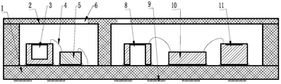
- 3 and 4 are schematic views showing the structure of the first embodiment of the integrated sensor package structure of the present invention.
- 5 and 6 are schematic structural views of a second embodiment of the integrated sensor package structure of the present invention.
- FIG. 7 and 8 are schematic structural views of a third embodiment of the integrated sensor package structure of the present invention.
- 9 and 10 are schematic views showing the structure of a fourth embodiment of the integrated sensor package structure of the present invention.
- FIG. 11 is a schematic structural view of a fifth embodiment of the integrated sensor package structure of the present invention.
- 12 and 13 are schematic views showing the structure of a sixth embodiment of the integrated sensor package structure of the present invention.
- 14 and 15 are schematic views showing the structure of a seventh embodiment of the integrated sensor package structure of the present invention.
- 16 and 17 are schematic views showing the structure of an eighth embodiment of the integrated sensor package structure of the present invention.
- 18 and 19 are schematic views showing the structure of a ninth embodiment of the integrated sensor package structure of the present invention.
- the integrated sensor includes a plurality of sensor units, some of which are relatively more sensitive, ie, more susceptible to interference from other sensor units in the integrated sensor, where the sensor unit that is susceptible to interference from other sensor units is referred to as a "sensitive sensor. Sensor units outside the sensitive sensor are called “non-sensitive sensors.”
- the present invention isolates each sensitive sensor from other sensors, and further isolates any sensor from other sensors. For example, in an integrated sensor including a pressure sensor, a microphone, and a humidity sensor, the pressure sensor releases electromagnetic signals and heat energy as a source of interference, the microphone is easily interfered by the electromagnetic signal emitted by the pressure sensor, and the humidity sensor is easily replaced by the pressure sensor.
- the pressure sensor is a non-sensitive sensor
- the microphone and humidity sensor are sensitive sensors
- the present invention isolates the microphone from other sensors and isolates the humidity sensor from other sensors. Based on the disclosure of the present invention, those skilled in the art can determine sensitive sensors and non-sensitive sensors according to actual application products and environments, and these should also fall within the protection scope of the present invention.
- a first embodiment of an integrated sensor package structure includes two sensor units, one of which includes a MEMS sensor chip 3 and an ASIC chip 5, and a lead 4 is passed between the two. Electrically connected, the ASIC chip 5 is electrically connected to the first substrate 1 through a lead.
- the other sensor unit includes a MEMS sensor chip 8 and an ASIC chip 7, which are also electrically connected by a lead, and the ASIC chip 7 is electrically connected to the first substrate 1 through a lead. Both sensor units are mounted on the first substrate 1, and are electrically connected to an external circuit through the pads 9 on the back surface of the first substrate 1.
- the first embodiment is to form a large package cavity (first package cavity) through the outer casing 2 and the first substrate 1, and to provide a sidewall in the large package cavity to isolate the large package cavity into two Small package cavity (second package cavity), two The sensor units are respectively disposed in the respective second package cavities, and an opening 6 required for sensor unit sensing is opened at the top of the second package cavity.
- a second embodiment of the integrated sensor package structure is different from the first embodiment shown in FIG. 3 in that the second embodiment further includes a third sensor unit, and a third
- the sensor unit includes a MEMS sensor chip 11 and an ASIC chip 10, which are also electrically connected by wires, and the ASIC chip 10 is electrically connected to the first substrate 1 through leads.
- Providing sidewalls inside the large package cavity (first package cavity) separates the large package cavity into three small package cavities (second package cavities), and the three sensor units are respectively disposed in the respective second package cavities in vivo.
- a third embodiment of an integrated sensor package structure includes three sensor units including one sensitive sensor and two non-sensitive sensors, and the sensitive sensor unit includes a MEMS sensor chip 3 and an ASIC chip 5, One non-sensitive sensor unit includes a MEMS sensor chip 8 and an ASIC chip 7, and the other non-sensitive sensor unit includes a MEMS sensor chip 11 and an ASIC chip 10.
- Providing a sidewall inside the large package cavity separates the large package cavity (first package cavity) into two small package cavities (the second package cavity), and the sensitive sensor is separately disposed in a second package cavity
- the two non-sensitive sensors are collectively disposed in another second package cavity to isolate the sensitive sensor from other sensors, and the sensitive sensor unit is prevented from being interfered by other sensor units.
- a fourth embodiment of the integrated sensor package structure is different from the first embodiment shown in FIG. 3 in that the small package is not isolated by providing sidewalls inside the large package cavity.
- the form of the cavity realizes the isolation between different sensor units, but is a separate third package cavity surrounded by two independent housings 2-1 and 2-2, respectively, with the first substrate 1, two sensor units They are respectively disposed in the respective third package cavities, and the openings 6-1 and 6-2 required for sensor unit sensing are respectively opened on the top of the third package cavity.
- a fifth embodiment of the integrated sensor package structure is different from the fourth embodiment shown in FIG. 9 in that the sensor unit on the right side is not directly disposed on the first substrate 1 but passes through the second The substrate 15 is indirectly disposed on the first substrate 1.
- the sensor unit is mounted on the second substrate 15, and is electrically connected to an external circuit through the pad 9 on the back surface of the first substrate 1.
- external stress is transmitted to the first substrate 1 and then by the second
- the substrate 15 is buffered and removed, and the sensor unit is protected to make the performance of the sensor unit more stable.
- the second substrate 15 is designed as a buffer portion, which avoids the influence of external stress on the pressure sensor and causes pressure sensor data error, thereby improving the sensitivity of the pressure sensor unit.
- the outer casings in the first to third embodiments are composed of a substrate
- the outer casings in the fourth and fifth embodiments are metal outer casings.
- each chip needs to be separately mounted and electrically connected, the process is low in efficiency, the hidden dangers are sharply increased, and the assembled safety space needs to be left between the chips, thereby wasting the overall space of the product.
- the invention can also integrate the sensor unit to reduce space waste, optimize the processing procedure, and improve the packaging efficiency and product yield.
- the present invention provides the following three integration methods:
- a sixth embodiment of the integrated sensor package structure includes three sensor units as in the second embodiment shown in Figure 5, except that the MEMS sensor chip of the left sensor unit 21 and The ASIC chips are integrated and the MEMS sensor chip and ASIC chip of the intermediate sensor unit 22 are integrated.
- a seventh embodiment of the integrated sensor package structure is different from the third embodiment shown in FIG. 7 in that two sensor units that do not interfere with each other share an ASIC chip, specifically It is said that the MEMS sensor chip 8 and the MEMS sensor chip 11 share one ASIC chip 10.
- an eighth embodiment of the integrated sensor package structure is different from the third embodiment shown in FIG. 7 in that two sensor units that do not interfere with each other share a MEMS sensor chip.
- the ASIC chip 7 and the ASIC chip 10 share a MEMS sensor chip 8.
- a third embodiment of the integrated sensor package structure is different from the third embodiment shown in FIG. 7 in that the MEMS sensor chip and the ASIC chip of the intermediate non-sensitive sensor unit 22 are integrated. Together, another non-sensitive sensor unit on the right (including the MEMS sensor chip 11 and the ASIC chip 10) does not interfere with sharing a cavity.
- the present invention separates each sensor unit of the integrated sensor by cavity separation, or is susceptible to being susceptible to The sensitive sensor unit to the interference is isolated and encapsulated to shield the mutual interference between the individual sensor units of the integrated sensor, thereby effectively improving the performance of the integrated sensor.
Landscapes
- Engineering & Computer Science (AREA)
- Computer Hardware Design (AREA)
- Microelectronics & Electronic Packaging (AREA)
- Micromachines (AREA)
Abstract
一种集成传感器的封装结构,包括:第一基板(1)以及设置在第一基板(1)上的多个传感器,每个传感器均包括MEMS传感器芯片(3,8,11)和与MEMS传感器芯片电连接的ASIC芯片(5,7,10);其中,每个传感器均与其它传感器隔离地封装在第一基板(1)上。一种集成传感器的封装结构,传感器包括敏感传感器和非敏感传感器,每个敏感传感器均与其它传感器隔离地封装在第一基板(1)上。通过腔体分离,将集成传感器的每个传感器单元都进行隔离封装,或者将容易受到干扰的敏感传感器单元进行隔离封装,以屏蔽掉集成传感器的各个传感器单元之间的彼此干扰,有效提升了集成传感器的产品性能。
Description
本发明涉及集成传感器的封装结构。
集成传感器是一种内部集成了多个传感器单元的传感器芯片(例如由压力传感器单元和温度传感器单元集成的集成传感器),并且作为一个能够同时实现多种传感功能的独立的芯片进行使用。目前集成传感器的封装一般是将其各个传感器单元的MEMS传感器芯片和ASIC芯片贴装于基板上,最终封装在一个腔体内进行集成,例如图1和图2所示:外壳2覆盖在第一基板1上围成一个大的腔体,腔体内设置有贴装在第一基板1上的两个传感器单元。其中一个传感器单元包括MEMS传感器芯片3和ASIC芯片5,两者之间通过引线4电连接,AISC芯片5通过引线连接至第一基板1。另一个传感器单元包括MEMS传感器芯片8和ASIC芯片7,两者之间同样通过引线电连接,AISC芯片7通过引线连接至第一基板1。外壳2设有传感器单元传感所需的开口6,第一基板1的背面设有焊盘9,传感器单元通过焊盘9与外部电路电连接。
现有集成传感器的这种封装方式是将集成传感器的全部传感器单元封装在一个腔体内,这种情况下不同传感器单元之间容易造成电、磁、热、光等相互干扰,严重影响集成传感器的整体性能。
发明内容
为了解决上述技术问题,尽量减少集成传感器的各个传感器单元之间的互相干扰,本发明提出了关于集成传感器封装的新的技术方案。
根据本发明的第一方面,提供了一种集成传感器的封装结构,包括:第一基板以及设置在所述第一基板上的多个传感器,每个所述传感器均包
括MEMS传感器芯片和与所述MEMS传感器芯片电连接的ASIC芯片;其中,每个所述传感器均与其它传感器隔离地封装在所述第一基板上。
优选的,包括至少一个由外壳和所述第一基板围成的第一封装腔体,所述第一封装腔体内通过侧壁隔离为至少两个第二封装腔体,每个所述第二封装腔体内设置有一个所述传感器。
优选的,包括至少一个由独立外壳和所述第一基板围成的第三封装腔体,每个所述第三封装腔体内部设置有一个所述传感器。
优选的,所述传感器直接设置于所述第一基板上或者通过第二基板设置于所述第一基板上。
优选的,至少一个所述传感器的MEMS传感器芯片和ASIC芯片集成在一起。
优选的,互不干扰的传感器的ASIC芯片集成在一起或者MEMS传感器芯片集成在一起。
根据本发明的第二方面,还提供了一种集成传感器的封装结构,包括:第一基板以及设置在所述第一基板上的多个传感器,每个所述传感器均包括MEMS传感器芯片和与所述MEMS传感器芯片电连接的ASIC芯片;其中,所述传感器包括敏感传感器和非敏感传感器,每个所述敏感传感器均与其它传感器隔离地封装在所述第一基板上。
优选的,包括至少一个由外壳和所述第一基板围成的第一封装腔体,所述第一封装腔体内通过侧壁隔离为至少两个第二封装腔体,其中至少一个第二封装腔体内设置有一个所述敏感传感器。
优选的,包括至少一个由独立外壳和所述第一基板围成的第三封装腔体,其中至少一个第三封装腔体内部设置有一个所述敏感传感器。
优选的,多个所述传感器包括压力传感器、麦克风、以及湿度传感器,所述麦克风和所述湿度传感为敏感传感器,所述压力传感器为非敏感传感器。
优选的,所述传感器直接设置于所述第一基板上或者通过第二基板设置于所述第一基板上。
优选的,至少一个所述传感器的MEMS传感器芯片和ASIC芯片集成
在一起。
优选的,互不干扰的传感器的ASIC芯片集成在一起或者MEMS传感器芯片集成在一起。
本发明通过腔体分立,将集成传感器的每个传感器单元都进行隔离封装,或者将容易受到干扰的敏感传感器单元进行隔离封装,以屏蔽掉集成传感器的各个传感器单元之间的彼此干扰,有效提升了集成传感器的产品性能。
构成说明书的一部分的附图描述了本发明的实施例,并且连同说明书一起用于解释本发明的原理。
图1、2是现有集成传感器封装结构的结构示意图。
图3、4是本发明集成传感器封装结构第一实施例的结构示意图。
图5、6是本发明集成传感器封装结构第二实施例的结构示意图。
图7、8是本发明集成传感器封装结构第三实施例的结构示意图。
图9、10是本发明集成传感器封装结构第四实施例的结构示意图。
图11是本发明集成传感器封装结构第五实施例的结构示意图。
图12、13是本发明集成传感器封装结构第六实施例的结构示意图。
图14、15是本发明集成传感器封装结构第七实施例的结构示意图。
图16、17是本发明集成传感器封装结构第八实施例的结构示意图。
图18、19是本发明集成传感器封装结构第九实施例的结构示意图。
现在将参照附图来详细描述本发明的各种示例性实施例。应注意到:除非另外具体说明,否则在这些实施例中阐述的部件和步骤的相对布置、数字表达式和数值不限制本发明的范围。
以下对至少一个示例性实施例的描述实际上仅仅是说明性的,决不作为对本发明及其应用或使用的任何限制。
对于相关领域普通技术人员已知的技术和设备可能不作详细讨论,但
在适当情况下,所述技术和设备应当被视为说明书的一部分。
在这里示出和讨论的所有例子中,任何具体值应被解释为仅仅是示例性的,而不是作为限制。因此,示例性实施例的其它例子可以具有不同的值。
应注意到:相似的标号和字母在下面的附图中表示类似项,因此,一旦某一项在一个附图中被定义,则在随后的附图中不需要对其进行进一步讨论。
集成传感器中包括多个传感器单元,其中某些传感器单元相对更为敏感,即更容易受到集成传感器中的其它传感器单元的干扰,这里将容易受到其它传感器单元干扰的传感器单元称之为“敏感传感器”,敏感传感器之外的传感器单元称之为“非敏感传感器”。本发明令每个敏感传感器均与其它传感器隔离,进一步也可以令任何一个传感器均与其它传感器隔离。例如在一个包括压力传感器、麦克风、以及湿度传感器的集成传感器中,压力传感器会释放电磁信号和热能成为干扰源,麦克风很容易被压力传感器释放出的电磁信号所干扰,湿度传感器很容易被压力传感器释放出的热能所干扰,所以压力传感器为非敏感传感器,麦克风和湿度传感器为敏感传感器,所以本发明会将麦克风与其它传感器隔离开,将湿度传感器也与其它传感器隔离开。在本发明公开的基础上,本领域技术人员可以根据实际应用产品和环境确定敏感传感器和非敏感传感器,这些也应当属于本发明的保护范围内。
参考图3和图4所示为集成传感器封装结构的第一实施例,集成传感器一共包含两个传感器单元,其中一个传感器单元包括MEMS传感器芯片3和ASIC芯片5,两者之间通过一引线4电连接,ASIC芯片5通过一引线与第一基板1电连接。另一个传感器单元包括MEMS传感器芯片8和ASIC芯片7,两者之间同样通过一引线电连接,ASIC芯片7通过一引线与第一基板1电连接。两个传感器单元均贴装于第一基板1上,通过第一基板1背面的焊盘9与外部电路电连接。可以看出,第一实施例是通过外壳2和第一基板1围成一个大封装腔体(第一封装腔体),在大封装腔体内部设置侧壁将大封装腔体隔离为两个小封装腔体(第二封装腔体),两
个传感器单元分别设置于各自的第二封装腔体内,在第二封装腔体的顶部开设有传感器单元传感所需的开口6。
参考图5和图6所示为集成传感器封装结构的第二实施例,和图3所示的第一实施例的不同之处在于,第二实施例还包括第三个传感器单元,第三个传感器单元包括MEMS传感器芯片11和ASIC芯片10,两者之间同样通过引线电连接,ASIC芯片10通过引线与第一基板1电连接。在大封装腔体(第一封装腔体)内部设置侧壁将大封装腔体隔离为三个小封装腔体(第二封装腔体),三个传感器单元分别设置于各自的第二封装腔体内。
参考图7和图8所示为集成传感器封装结构的第三实施例,包括三个传感器单元,其中包括一个敏感传感器和两个非敏感传感器,敏感传感器单元包括MEMS传感器芯片3和ASIC芯片5,一个非敏感传感器单元包括MEMS传感器芯片8和ASIC芯片7,另一个非敏感传感器单元包括MEMS传感器芯片11和ASIC芯片10。在大封装腔体内部设置侧壁将大封装腔体(第一封装腔体)隔离为两个小封装腔体(第二封装腔体),将敏感传感器单独的设置于一个第二封装腔体内,将两个非敏感传感器共同设置在另一个第二封装腔体内,以实现敏感传感器和其它传感器的隔离,避免敏感传感器单元受到其它传感器单元的干扰。
参考图9和图10所示为集成传感器封装结构的第四实施例,和图3所示的第一实施例的不同之处在于,不是通过在大封装腔体内部设置侧壁隔离出小封装腔体的形式实现不同传感器单元之间的隔离,而是由两个彼此独立的外壳2-1和2-2分别与第一基板1围成的独立的第三封装腔体,两个传感器单元分别设置于各自的第三封装腔体内,在第三封装腔体的顶部分别开设有传感器单元传感所需的开口6-1和6-2。
参考图11所示为集成传感器封装结构的第五实施例,和图9所示的第四实施例的不同之处在于,右边的传感器单元不是直接设置于第一基板1上而是通过第二基板15间接设置于所述第一基板1上,该传感器单元贴装于第二基板15上,通过第一基板1背面的焊盘9与外部电路电连接。在该传感器单元的装配、工作过程中,外部应力传递至第一基板1然后由第二
基板15缓冲卸掉,保护了该传感器单元,使该传感器单元性能更稳定。特别对于压力传感器单元,第二基板15作为缓冲部的结构设计,避免了外部应力对压力传感器产生影响而导致压力传感器数据误差,提高了压力传感器单元的灵敏度。
其中,第一至第三实施例中的外壳是由基板组成,第四和第五实施例中的外壳是金属外壳。
上述实施例中,各个芯片需要单独贴装和电连接,工序多效率低,不良隐患剧增,并且各个芯片之间需要留出组装安全空间,浪费产品总体空间。为了能够更好的实现腔体的分立,本发明还可以将传感器单元进行集成设计,以减少空间浪费,优省加工工序,提升封装效率和产品良率。本发明提供了以下三种集成方式:
参考图12和图13所示为集成传感器封装结构的第六实施例,和图5所示的第二实施例一样包括三个传感器单元,不同之处在于,左边传感器单元21的MEMS传感器芯片和ASIC芯片集成在一起,中间传感器单元22的MEMS传感器芯片和ASIC芯片集成在一起。
参考图14和图15所示为集成传感器封装结构的第七实施例,和图7所示的第三实施例的不同之处在于,两个互不干扰的传感器单元共用一个ASIC芯片,具体来说MEMS传感器芯片8和MEMS传感器芯片11共用一个ASIC芯片10。
参考图16和图17所示为集成传感器封装结构的第八实施例,和图7所示的第三实施例的不同之处在于,两个互不干扰的传感器单元共用一个MEMS传感器芯片,具体来说ASIC芯片7和ASIC芯片10共用一个MEMS传感器芯片8。
参考图18和图19所示为集成传感器封装结构的第三实施例,和图7所示的第三实施例的不同之处在于,中间的非敏感传感器单元22的MEMS传感器芯片和ASIC芯片集成在一起,和右边的另一个非敏感传感器单元(包括MEMS传感器芯片11和ASIC芯片10)互不干扰共用一个腔体。
相对于现有的集成传感器共用一个大腔体的封装方式,本发明通过腔体分立,将集成传感器的每个传感器单元都进行隔离封装,或者将容易受
到干扰的敏感传感器单元进行隔离封装,以屏蔽掉集成传感器的各个传感器单元之间的彼此干扰,有效提升了集成传感器的产品性能。
虽然已经通过例子对本发明的一些特定实施例进行了详细说明,但是本领域的技术人员应该理解,以上例子仅是为了进行说明,而不是为了限制本发明的范围。本领域的技术人员应该理解,可在不脱离本发明的范围和精神的情况下,对以上实施例进行修改。本发明的范围由所附权利要求来限定。
Claims (10)
- 一种集成传感器的封装结构,其特征在于,包括:第一基板以及设置在所述第一基板上的多个传感器,每个所述传感器均包括MEMS传感器芯片和与所述MEMS传感器芯片电连接的ASIC芯片;其中,每个所述传感器均与其它传感器隔离地封装在所述第一基板上。
- 根据权利要求1所述的结构,其特征在于,包括至少一个由外壳和所述第一基板围成的第一封装腔体,所述第一封装腔体内通过侧壁隔离为至少两个第二封装腔体,每个所述第二封装腔体内设置有一个所述传感器。
- 根据权利要求1所述的结构,其特征在于,包括至少一个由独立外壳和所述第一基板围成的第三封装腔体,每个所述第三封装腔体内部设置有一个所述传感器。
- 一种集成传感器的封装结构,其特征在于,包括:第一基板以及设置在所述第一基板上的多个传感器,每个所述传感器均包括MEMS传感器芯片和与所述MEMS传感器芯片电连接的ASIC芯片;其中,所述传感器包括敏感传感器和非敏感传感器,每个所述敏感传感器均与其它传感器隔离地封装在所述第一基板上。
- 根据权利要求4所述的结构,其特征在于,包括至少一个由外壳和所述第一基板围成的第一封装腔体,所述第一封装腔体内通过侧壁隔离为至少两个第二封装腔体,其中至少一个第二封装腔体内设置有一个所述敏感传感器。
- 根据权利要求4所述的结构,其特征在于,包括至少一个由独立外壳和所述第一基板围成的第三封装腔体,其中至少一个第三封装腔体内部设置有一个所述敏感传感器。
- 根据权利要求4-6任一项所述的结构,其特征在于,多个所述传感器包括压力传感器、麦克风、以及湿度传感器,所述麦克风和所述湿度传感为敏感传感器,所述压力传感器为非敏感传感器。
- 根据权利要求1或4所述的结构,其特征在于,所述传感器直接设置于所述第一基板上或者通过第二基板设置于所述第一基板上。
- 根据权利要求1或4所述的结构,其特征在于,至少一个所述传感器的MEMS传感器芯片和ASIC芯片集成在一起。
- 根据权利要求1或4所述的结构,其特征在于,互不干扰的传感器的ASIC芯片集成在一起或者MEMS传感器芯片集成在一起。
Applications Claiming Priority (2)
| Application Number | Priority Date | Filing Date | Title |
|---|---|---|---|
| CN201510182343.9A CN104779214A (zh) | 2015-04-16 | 2015-04-16 | 集成传感器的封装结构 |
| CN201510182343.9 | 2015-04-16 |
Publications (1)
| Publication Number | Publication Date |
|---|---|
| WO2016165359A1 true WO2016165359A1 (zh) | 2016-10-20 |
Family
ID=53620610
Family Applications (1)
| Application Number | Title | Priority Date | Filing Date |
|---|---|---|---|
| PCT/CN2015/096909 Ceased WO2016165359A1 (zh) | 2015-04-16 | 2015-12-10 | 集成传感器的封装结构 |
Country Status (2)
| Country | Link |
|---|---|
| CN (1) | CN104779214A (zh) |
| WO (1) | WO2016165359A1 (zh) |
Cited By (1)
| Publication number | Priority date | Publication date | Assignee | Title |
|---|---|---|---|---|
| CN112509926A (zh) * | 2020-12-03 | 2021-03-16 | 山东傲天环保科技有限公司 | 一种多芯片封装结构及其制造方法 |
Families Citing this family (10)
| Publication number | Priority date | Publication date | Assignee | Title |
|---|---|---|---|---|
| CN104779214A (zh) * | 2015-04-16 | 2015-07-15 | 歌尔声学股份有限公司 | 集成传感器的封装结构 |
| WO2017205533A1 (en) * | 2016-05-26 | 2017-11-30 | Knowles Electronics, Llc | Microphone device with integrated pressure sensor |
| CN107271029A (zh) * | 2017-06-06 | 2017-10-20 | 纽威仕微电子(无锡)有限公司 | 一种水听器集成模块及其制造工艺 |
| CN109368588A (zh) * | 2018-12-07 | 2019-02-22 | 歌尔股份有限公司 | 芯片内置电路板、组合传感器及电子设备 |
| CN109348389B (zh) * | 2018-12-07 | 2024-05-24 | 歌尔微电子股份有限公司 | 组合传感器和电子设备 |
| CN110118702A (zh) * | 2019-04-23 | 2019-08-13 | 瑞声声学科技(深圳)有限公司 | 一种玻璃破碎检测装置及方法 |
| CN110470700B (zh) * | 2019-07-11 | 2022-08-02 | 维沃移动通信有限公司 | 传感器组件、传感器及终端设备 |
| CN112701211B (zh) * | 2020-12-29 | 2023-04-28 | 上海烨映微电子科技股份有限公司 | 红外热电堆封装结构及方法 |
| CN114440954A (zh) * | 2021-12-28 | 2022-05-06 | 荣成歌尔微电子有限公司 | 传感器封装结构、封装方法及电子设备 |
| TWI905873B (zh) * | 2024-08-13 | 2025-11-21 | 國立臺灣海洋大學 | 多功能感測裝置 |
Citations (5)
| Publication number | Priority date | Publication date | Assignee | Title |
|---|---|---|---|---|
| CN102413409A (zh) * | 2011-12-17 | 2012-04-11 | 歌尔声学股份有限公司 | Mems麦克风 |
| CN102740206A (zh) * | 2011-04-02 | 2012-10-17 | 哈曼国际工业有限公司 | 双单元微机电系统组件 |
| CN103500770A (zh) * | 2013-10-23 | 2014-01-08 | 中北大学 | 一种多气体检测的红外气体传感器 |
| CN104229730A (zh) * | 2013-06-20 | 2014-12-24 | 霍尼韦尔国际公司 | Mems装置的封装方法 |
| CN104779214A (zh) * | 2015-04-16 | 2015-07-15 | 歌尔声学股份有限公司 | 集成传感器的封装结构 |
Family Cites Families (6)
| Publication number | Priority date | Publication date | Assignee | Title |
|---|---|---|---|---|
| CN1960580B (zh) * | 2005-11-03 | 2011-06-29 | 歌尔声学股份有限公司 | 适于量产的硅麦克风封装 |
| DE102009027382A1 (de) * | 2009-07-01 | 2011-01-05 | Robert Bosch Gmbh | Elektronisches Bauteil mit EMV-Schutz |
| CN102020232A (zh) * | 2009-09-09 | 2011-04-20 | 美律实业股份有限公司 | 微机电声学感测器封装结构 |
| US8809784B2 (en) * | 2010-10-21 | 2014-08-19 | Raytheon Company | Incident radiation detector packaging |
| CN103968886A (zh) * | 2013-02-04 | 2014-08-06 | 刘胜 | 一种多自由度微传感器模块及其封装 |
| CN203820443U (zh) * | 2013-07-18 | 2014-09-10 | 瑞声声学科技(深圳)有限公司 | Mems封装 |
-
2015
- 2015-04-16 CN CN201510182343.9A patent/CN104779214A/zh active Pending
- 2015-12-10 WO PCT/CN2015/096909 patent/WO2016165359A1/zh not_active Ceased
Patent Citations (5)
| Publication number | Priority date | Publication date | Assignee | Title |
|---|---|---|---|---|
| CN102740206A (zh) * | 2011-04-02 | 2012-10-17 | 哈曼国际工业有限公司 | 双单元微机电系统组件 |
| CN102413409A (zh) * | 2011-12-17 | 2012-04-11 | 歌尔声学股份有限公司 | Mems麦克风 |
| CN104229730A (zh) * | 2013-06-20 | 2014-12-24 | 霍尼韦尔国际公司 | Mems装置的封装方法 |
| CN103500770A (zh) * | 2013-10-23 | 2014-01-08 | 中北大学 | 一种多气体检测的红外气体传感器 |
| CN104779214A (zh) * | 2015-04-16 | 2015-07-15 | 歌尔声学股份有限公司 | 集成传感器的封装结构 |
Cited By (2)
| Publication number | Priority date | Publication date | Assignee | Title |
|---|---|---|---|---|
| CN112509926A (zh) * | 2020-12-03 | 2021-03-16 | 山东傲天环保科技有限公司 | 一种多芯片封装结构及其制造方法 |
| CN112509926B (zh) * | 2020-12-03 | 2022-07-22 | 山东博通微电子有限公司 | 一种多芯片封装结构及其制造方法 |
Also Published As
| Publication number | Publication date |
|---|---|
| CN104779214A (zh) | 2015-07-15 |
Similar Documents
| Publication | Publication Date | Title |
|---|---|---|
| CN104779213B (zh) | 集成传感器的封装结构和封装方法 | |
| WO2016165360A1 (zh) | 一种集成传感器的封装结构 | |
| CN104779214A (zh) | 集成传感器的封装结构 | |
| US11268859B2 (en) | Wearable infrared temperature sensing device | |
| CN104900599A (zh) | 集成传感器的封装结构和封装方法 | |
| TWI726788B (zh) | 振動感測器 | |
| CN104620082B (zh) | 在传感器单元与防爆外壳之间的接口 | |
| CN204464255U (zh) | 集成传感器的封装结构 | |
| US9319772B2 (en) | Multi-floor type MEMS microphone | |
| US20160023891A1 (en) | Component including a MEMS element and a cap structure including a media connection port | |
| CN106298704B (zh) | 一种带热沉和磁屏蔽的mems封装及其制备方法 | |
| CN102738132A (zh) | 包括光学半导体器件的半导体封装体 | |
| CN105466627B (zh) | 用于测量流体压力的传感器模块 | |
| TW201011887A (en) | Integrated circuit chip and seal ring structure of an integrated circuit chip | |
| US20140161289A1 (en) | Silicon Condenser Microphone | |
| US20170096331A1 (en) | Mems element including a stress decoupling structure and a component including such a mems element | |
| US10474200B2 (en) | Optical module having shield structure in feedthrough | |
| US20140374847A1 (en) | Packaging method for mems devices | |
| CN204516738U (zh) | 集成传感器的封装结构 | |
| CN204464257U (zh) | 集成传感器的封装结构 | |
| CN209057368U (zh) | 一种芯片的封装结构及电子设备 | |
| US10254186B2 (en) | Pressure sensor | |
| US10694297B1 (en) | Back chamber volume enlargement microphone package | |
| CN207475875U (zh) | 一种麦克风、环境传感器的封装结构 | |
| CN204464258U (zh) | 一种集成传感器的封装结构 |
Legal Events
| Date | Code | Title | Description |
|---|---|---|---|
| 121 | Ep: the epo has been informed by wipo that ep was designated in this application |
Ref document number: 15889055 Country of ref document: EP Kind code of ref document: A1 |
|
| NENP | Non-entry into the national phase |
Ref country code: DE |
|
| 32PN | Ep: public notification in the ep bulletin as address of the adressee cannot be established |
Free format text: NOTING OF LOSS OF RIGHTS PURSUANT TO RULE 112(1) EPC (EPO FORM 1205A DATED 12.04.2018) |
|
| 122 | Ep: pct application non-entry in european phase |
Ref document number: 15889055 Country of ref document: EP Kind code of ref document: A1 |