WO2016158697A1 - 埋め込み平坦化膜の製造方法及び電子デバイスの製造方法 - Google Patents
埋め込み平坦化膜の製造方法及び電子デバイスの製造方法 Download PDFInfo
- Publication number
- WO2016158697A1 WO2016158697A1 PCT/JP2016/059482 JP2016059482W WO2016158697A1 WO 2016158697 A1 WO2016158697 A1 WO 2016158697A1 JP 2016059482 W JP2016059482 W JP 2016059482W WO 2016158697 A1 WO2016158697 A1 WO 2016158697A1
- Authority
- WO
- WIPO (PCT)
- Prior art keywords
- film
- coating
- solvent
- embedded
- planarization film
- Prior art date
- Legal status (The legal status is an assumption and is not a legal conclusion. Google has not performed a legal analysis and makes no representation as to the accuracy of the status listed.)
- Ceased
Links
Images



Classifications
-
- H—ELECTRICITY
- H10—SEMICONDUCTOR DEVICES; ELECTRIC SOLID-STATE DEVICES NOT OTHERWISE PROVIDED FOR
- H10W—GENERIC PACKAGES, INTERCONNECTIONS, CONNECTORS OR OTHER CONSTRUCTIONAL DETAILS OF DEVICES COVERED BY CLASS H10
- H10W20/00—Interconnections in chips, wafers or substrates
- H10W20/01—Manufacture or treatment
- H10W20/031—Manufacture or treatment of conductive parts of the interconnections
- H10W20/062—Manufacture or treatment of conductive parts of the interconnections by smoothing of conductive parts, e.g. by planarisation
-
- H—ELECTRICITY
- H10—SEMICONDUCTOR DEVICES; ELECTRIC SOLID-STATE DEVICES NOT OTHERWISE PROVIDED FOR
- H10P—GENERIC PROCESSES OR APPARATUS FOR THE MANUFACTURE OR TREATMENT OF DEVICES COVERED BY CLASS H10
- H10P95/00—Generic processes or apparatus for manufacture or treatments not covered by the other groups of this subclass
- H10P95/06—Planarisation of inorganic insulating materials
-
- C—CHEMISTRY; METALLURGY
- C08—ORGANIC MACROMOLECULAR COMPOUNDS; THEIR PREPARATION OR CHEMICAL WORKING-UP; COMPOSITIONS BASED THEREON
- C08G—MACROMOLECULAR COMPOUNDS OBTAINED OTHERWISE THAN BY REACTIONS ONLY INVOLVING UNSATURATED CARBON-TO-CARBON BONDS
- C08G73/00—Macromolecular compounds obtained by reactions forming a linkage containing nitrogen with or without oxygen or carbon in the main chain of the macromolecule, not provided for in groups C08G12/00 - C08G71/00
- C08G73/02—Polyamines
- C08G73/0206—Polyalkylene(poly)amines
-
- C—CHEMISTRY; METALLURGY
- C09—DYES; PAINTS; POLISHES; NATURAL RESINS; ADHESIVES; COMPOSITIONS NOT OTHERWISE PROVIDED FOR; APPLICATIONS OF MATERIALS NOT OTHERWISE PROVIDED FOR
- C09D—COATING COMPOSITIONS, e.g. PAINTS, VARNISHES OR LACQUERS; FILLING PASTES; CHEMICAL PAINT OR INK REMOVERS; INKS; CORRECTING FLUIDS; WOODSTAINS; PASTES OR SOLIDS FOR COLOURING OR PRINTING; USE OF MATERIALS THEREFOR
- C09D179/00—Coating compositions based on macromolecular compounds obtained by reactions forming in the main chain of the macromolecule a linkage containing nitrogen, with or without oxygen, or carbon only, not provided for in groups C09D161/00 - C09D177/00
- C09D179/02—Polyamines
-
- H—ELECTRICITY
- H10—SEMICONDUCTOR DEVICES; ELECTRIC SOLID-STATE DEVICES NOT OTHERWISE PROVIDED FOR
- H10P—GENERIC PROCESSES OR APPARATUS FOR THE MANUFACTURE OR TREATMENT OF DEVICES COVERED BY CLASS H10
- H10P14/00—Formation of materials, e.g. in the shape of layers or pillars
- H10P14/60—Formation of materials, e.g. in the shape of layers or pillars of insulating materials
- H10P14/63—Formation of materials, e.g. in the shape of layers or pillars of insulating materials characterised by the formation processes
- H10P14/6326—Deposition processes
- H10P14/6342—Liquid deposition, e.g. spin-coating, sol-gel techniques or spray coating
-
- H—ELECTRICITY
- H10—SEMICONDUCTOR DEVICES; ELECTRIC SOLID-STATE DEVICES NOT OTHERWISE PROVIDED FOR
- H10P—GENERIC PROCESSES OR APPARATUS FOR THE MANUFACTURE OR TREATMENT OF DEVICES COVERED BY CLASS H10
- H10P14/00—Formation of materials, e.g. in the shape of layers or pillars
- H10P14/60—Formation of materials, e.g. in the shape of layers or pillars of insulating materials
- H10P14/65—Formation of materials, e.g. in the shape of layers or pillars of insulating materials characterised by treatments performed before or after the formation of the materials
- H10P14/6516—Formation of materials, e.g. in the shape of layers or pillars of insulating materials characterised by treatments performed before or after the formation of the materials of treatments performed after formation of the materials
- H10P14/6534—Formation of materials, e.g. in the shape of layers or pillars of insulating materials characterised by treatments performed before or after the formation of the materials of treatments performed after formation of the materials by exposure to a liquid
-
- H—ELECTRICITY
- H10—SEMICONDUCTOR DEVICES; ELECTRIC SOLID-STATE DEVICES NOT OTHERWISE PROVIDED FOR
- H10P—GENERIC PROCESSES OR APPARATUS FOR THE MANUFACTURE OR TREATMENT OF DEVICES COVERED BY CLASS H10
- H10P14/00—Formation of materials, e.g. in the shape of layers or pillars
- H10P14/60—Formation of materials, e.g. in the shape of layers or pillars of insulating materials
- H10P14/65—Formation of materials, e.g. in the shape of layers or pillars of insulating materials characterised by treatments performed before or after the formation of the materials
- H10P14/6516—Formation of materials, e.g. in the shape of layers or pillars of insulating materials characterised by treatments performed before or after the formation of the materials of treatments performed after formation of the materials
- H10P14/6548—Formation of materials, e.g. in the shape of layers or pillars of insulating materials characterised by treatments performed before or after the formation of the materials of treatments performed after formation of the materials by forming intermediate materials, e.g. capping layers or diffusion barriers
-
- H—ELECTRICITY
- H10—SEMICONDUCTOR DEVICES; ELECTRIC SOLID-STATE DEVICES NOT OTHERWISE PROVIDED FOR
- H10P—GENERIC PROCESSES OR APPARATUS FOR THE MANUFACTURE OR TREATMENT OF DEVICES COVERED BY CLASS H10
- H10P14/00—Formation of materials, e.g. in the shape of layers or pillars
- H10P14/60—Formation of materials, e.g. in the shape of layers or pillars of insulating materials
- H10P14/68—Organic materials, e.g. photoresists
- H10P14/683—Organic materials, e.g. photoresists carbon-based polymeric organic materials, e.g. polyimides, poly cyclobutene or PVC
-
- H—ELECTRICITY
- H10—SEMICONDUCTOR DEVICES; ELECTRIC SOLID-STATE DEVICES NOT OTHERWISE PROVIDED FOR
- H10P—GENERIC PROCESSES OR APPARATUS FOR THE MANUFACTURE OR TREATMENT OF DEVICES COVERED BY CLASS H10
- H10P50/00—Etching of wafers, substrates or parts of devices
- H10P50/20—Dry etching; Plasma etching; Reactive-ion etching
- H10P50/28—Dry etching; Plasma etching; Reactive-ion etching of insulating materials
- H10P50/286—Dry etching; Plasma etching; Reactive-ion etching of insulating materials of organic materials
- H10P50/287—Dry etching; Plasma etching; Reactive-ion etching of insulating materials of organic materials by chemical means
-
- H—ELECTRICITY
- H10—SEMICONDUCTOR DEVICES; ELECTRIC SOLID-STATE DEVICES NOT OTHERWISE PROVIDED FOR
- H10P—GENERIC PROCESSES OR APPARATUS FOR THE MANUFACTURE OR TREATMENT OF DEVICES COVERED BY CLASS H10
- H10P95/00—Generic processes or apparatus for manufacture or treatments not covered by the other groups of this subclass
- H10P95/08—Planarisation of organic insulating materials
-
- H—ELECTRICITY
- H10—SEMICONDUCTOR DEVICES; ELECTRIC SOLID-STATE DEVICES NOT OTHERWISE PROVIDED FOR
- H10W—GENERIC PACKAGES, INTERCONNECTIONS, CONNECTORS OR OTHER CONSTRUCTIONAL DETAILS OF DEVICES COVERED BY CLASS H10
- H10W10/00—Isolation regions in semiconductor bodies between components of integrated devices
-
- H—ELECTRICITY
- H10—SEMICONDUCTOR DEVICES; ELECTRIC SOLID-STATE DEVICES NOT OTHERWISE PROVIDED FOR
- H10W—GENERIC PACKAGES, INTERCONNECTIONS, CONNECTORS OR OTHER CONSTRUCTIONAL DETAILS OF DEVICES COVERED BY CLASS H10
- H10W10/00—Isolation regions in semiconductor bodies between components of integrated devices
- H10W10/01—Manufacture or treatment
-
- H—ELECTRICITY
- H10—SEMICONDUCTOR DEVICES; ELECTRIC SOLID-STATE DEVICES NOT OTHERWISE PROVIDED FOR
- H10W—GENERIC PACKAGES, INTERCONNECTIONS, CONNECTORS OR OTHER CONSTRUCTIONAL DETAILS OF DEVICES COVERED BY CLASS H10
- H10W20/00—Interconnections in chips, wafers or substrates
- H10W20/01—Manufacture or treatment
- H10W20/031—Manufacture or treatment of conductive parts of the interconnections
- H10W20/032—Manufacture or treatment of conductive parts of the interconnections of conductive barrier, adhesion or liner layers
- H10W20/042—Manufacture or treatment of conductive parts of the interconnections of conductive barrier, adhesion or liner layers the barrier, adhesion or liner layers being seed or nucleation layers
- H10W20/045—Manufacture or treatment of conductive parts of the interconnections of conductive barrier, adhesion or liner layers the barrier, adhesion or liner layers being seed or nucleation layers for deposition from the gaseous phase, e.g. for chemical vapour deposition [CVD]
-
- H—ELECTRICITY
- H10—SEMICONDUCTOR DEVICES; ELECTRIC SOLID-STATE DEVICES NOT OTHERWISE PROVIDED FOR
- H10W—GENERIC PACKAGES, INTERCONNECTIONS, CONNECTORS OR OTHER CONSTRUCTIONAL DETAILS OF DEVICES COVERED BY CLASS H10
- H10W20/00—Interconnections in chips, wafers or substrates
- H10W20/01—Manufacture or treatment
- H10W20/031—Manufacture or treatment of conductive parts of the interconnections
- H10W20/032—Manufacture or treatment of conductive parts of the interconnections of conductive barrier, adhesion or liner layers
- H10W20/054—Manufacture or treatment of conductive parts of the interconnections of conductive barrier, adhesion or liner layers by selectively removing parts thereof
-
- H—ELECTRICITY
- H10—SEMICONDUCTOR DEVICES; ELECTRIC SOLID-STATE DEVICES NOT OTHERWISE PROVIDED FOR
- H10W—GENERIC PACKAGES, INTERCONNECTIONS, CONNECTORS OR OTHER CONSTRUCTIONAL DETAILS OF DEVICES COVERED BY CLASS H10
- H10W20/00—Interconnections in chips, wafers or substrates
- H10W20/01—Manufacture or treatment
- H10W20/031—Manufacture or treatment of conductive parts of the interconnections
- H10W20/056—Manufacture or treatment of conductive parts of the interconnections by filling conductive material into holes, grooves or trenches
Definitions
- the present invention relates to a method for manufacturing a buried planarizing film and a method for manufacturing an electronic device.
- a region including a concave portion of the member may be flattened by forming an embedded flattening film on the member having the concave portion.
- a trench embedding insulating film which is a two-layer insulating film, is applied to an element isolation groove of a semiconductor substrate (member) having an element isolation groove (concave portion) by a chemical vapor deposition method (CVD method) and a spin coating method.
- CVD method chemical vapor deposition method
- spin coating method A method of forming (embedded planarizing film) is known (see, for example, JP-A-11-150179).
- the embedded planarization film may be required to have heat resistance (for example, resistance to heat treatment that may be performed after the formation of the embedded planarization film).
- an object of the present invention is to provide a method for manufacturing an embedded planarization film that can form an embedded planarization film that is excellent in filling property (embedding property) into recesses and that has excellent heat resistance.
- the objective of this invention is providing the manufacturing method of an electronic device using the manufacturing method of the said embedded planarization film
- a method for manufacturing a buried planarizing film is forming a buried planarization film that planarizes a region including the concave portion of the member by applying a second coating liquid containing a solvent.
- ⁇ 2> The method for producing an embedded planarization film according to ⁇ 1>, wherein the organic substance having a carboxyl group is a divalent or higher carboxylic acid.
- ⁇ 3> The method for producing an embedded planarizing film according to ⁇ 1> or ⁇ 2>, wherein the content of the polyamine in the first coating solution is 1.0% by mass or more and 20% by mass or less.
- ⁇ 4> The method for producing an embedded planarization film according to any one of ⁇ 1> to ⁇ 3>, wherein the first solvent has a boiling point of 200 ° C. or lower and is hydrophilic.
- ⁇ 5> The method for manufacturing a buried planarizing film according to any one of ⁇ 1> to ⁇ 4>, wherein the buried planarizing film has an amide bond.
- ⁇ 6> The embedding according to any one of ⁇ 1> to ⁇ 5>, wherein the recess has a width of 250 nm or less and a ratio of depth to width [depth / width] is 0.3 or more.
- ⁇ 7> Any one of ⁇ 1> to ⁇ 6>, wherein the content per unit area of the metal element in the buried planarizing film is 5 ⁇ 10 10 atoms / cm 2 or less per one type of metal element
- the buried planarizing film is formed on the semiconductor substrate or the circuit board that is the member having the recess by the method for producing the buried planarizing film according to any one of ⁇ 1> to ⁇ 7>.
- a method for manufacturing an electronic device comprising a step of forming a buried planarizing film.
- the manufacturing method of the embedded planarization film which can form the embedded planarization film excellent in the filling property (embedding property) with respect to a recessed part and excellent in heat resistance is provided.
- a method for manufacturing an electronic device using the method for manufacturing a buried planarizing film is provided.
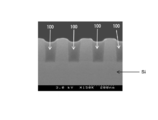
- Example 1 it is a scanning electron microscope (SEM) photograph (magnification 200000 times) which shows the section of the crevice (groove) buried with the embedding flattening film.
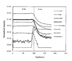
- 10 is a graph showing the results of TOF-SIMS measurement in Experimental Example 9.
- Example 2 it is a transmission electron microscope (TEM) photograph (magnification 100000 times) which shows the section of the crevice (groove) buried with the embedding flattening film.
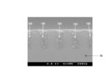
- Example 3 it is a scanning electron microscope (SEM) photograph (magnification 150,000 times) which shows the section of the crevice (groove) buried with the embedding flattening film.
- Example 4 it is a scanning electron microscope (SEM) photograph (magnification 150,000 times) which shows the section of the crevice (groove) buried with the embedding flattening film.
- Comparative example 1 it is a scanning electron microscope (SEM) photograph (magnification 150,000 times) which shows a section of a crevice (groove) in which a comparative film was formed.
- this embodiment a numerical range expressed using “to” means a range including numerical values described before and after “to” as a lower limit value and an upper limit value.
- the term “process” is not limited to an independent process, and even if it cannot be clearly distinguished from other processes, the term is used as long as the intended purpose of the process is achieved. include.
- the “coating film” means all films obtained by applying a coating solution.
- coating film includes not only a film in a state after application of a coating solution but before drying, but also a film in a state after coating of a coating solution and after drying, and after coating of a coating solution.
- a film in a state after heat treatment for example, soft bake described later, hard bake described later, etc.
- the thickness of the film may be referred to as “film thickness”.
- SP value in the present specification refers to Hansen solubility parameter, Hansen Solubility Parameter A User's Handbook (Charles M. Hansen al, CRC Press; 1 st Edition) according refers to a value calculated by the following equation.
- ⁇ (( ⁇ D) 2 + ( ⁇ P) 2 + ( ⁇ H) 2) 1/2 [Wherein ⁇ represents an SP value (ie, Hansen solubility parameter), ⁇ D represents a dispersion term, ⁇ P represents a polar term, and ⁇ H represents a hydrogen bond term. ]
- the method for manufacturing an embedded planarizing film according to the present embodiment includes a first coating liquid containing a polyamine and a first solvent in a region including the concave portion of a member having a concave portion.
- a second coating liquid containing a second solvent having a SP value of 30 (MPa) 1/2 or less and an SP value of 30 (MPa) or less an embedded flattening film for flattening the region including the concave portion of the member is formed.
- the manufacturing method of this embodiment may have another process as needed. Examples of other steps include known steps in a semiconductor process or a circuit board process.
- the embedded planarization film refers to a film having a function of planarizing a region including a concave portion of a member having a concave portion by at least partially filling (that is, filling) the concave portion.
- the embedded planarizing film may be formed (filled) only inside the recess (see, for example, FIG. 4), or formed (filled) inside the recess and then outside the recess (above the recess, and Further, it may be formed so as to protrude to a flat portion around the recess (for example, see FIGS. 1, 3 and 5).
- the manufacturing method of the present embodiment it is possible to form an embedded planarization film that has excellent filling properties (embedding properties) into the recesses and excellent heat resistance.
- the reason for this effect is considered as follows. That is, in the manufacturing method of the present embodiment, the buried planarizing film is formed by sequentially applying the first coating liquid and the second coating liquid to the region including the concave portion of the member having the concave portion.
- the first coating liquid is a liquid that is easy to reach the bottom of the concave portion and is easy to fill the concave portion (that is, easy to fill); and
- the second solvent in the second coating solution is a solvent that hardly dissolves (elutes) the polyamine filled in the recesses by application of the first coating solution, that is, the SP value is low (specifically, 30 (MPa) 1/2. (Below) by being a solvent It is considered that an embedded flattening film excellent in filling property (embedding property) to the concave portion can be formed.
- the polyamine in the first coating solution reacts with the organic substance having two or more carboxyl groups in the second coating solution in the concave portion of the member (preferably the amino acid of the polyamine). It is considered that at least one of an amide bond, an amide-imide bond, and an imide bond is formed by the group and the carboxyl group of the organic substance), and an embedded flattening film having excellent heat resistance can be formed.
- the second coating solution contains a second solvent having an SP value of 30 (MPa) 1/2 or less
- the second coating solution contains a second solvent having an SP value of 30 (MPa) 1/2 or less
- the second coating solution contains a second solvent having an SP value of 30 (MPa) 1/2 or less
- the second coating solution contains a second solvent having an SP value of 30 (MPa) 1/2 or less
- the second coating solution contains a second solvent having an SP value of 30 (MPa) 1/2 or less
- the second coating solution contains a second solvent having an SP value of 30 (MPa) 1/2 or less
- the present embodiment is made by paying attention to the fact that polyamine is easily dissolved in a solvent (for example, water) having an SP value of more than 30 (MPa) 1/2 . It has been completed as a means for suppressing a decrease in fillability. Furthermore, the present embodiment has been completed by finding that a film having excellent heat resistance can be obtained by a reaction between a polyamine and an organic substance having two or more carboxyl groups.
- a solvent for example, water
- the boiling point of the second solvent is 200 ° C. or less, the second solvent is less likely to remain in the embedded planarization film (for example, it is easily removed from the coating film by evaporation). Also have.
- the embedded planarization film manufactured by the manufacturing method of this embodiment is a film (preferably an amide) obtained by the reaction of polyamine and an organic substance having two or more carboxyl groups in the second coating solution. Therefore, it has excellent resistance to plasma (hereinafter also referred to as “plasma resistance”) that may be irradiated after the formation of the buried planarization film.
- plasma resistance include plasma generated from at least one gas selected from the group consisting of helium gas, argon gas, nitrogen gas, ammonia gas, and fluorocarbon-based gas.
- a polyimide film is widely known as a film excellent in heat resistance.
- the polyimide film tends to shrink after coating, and therefore, when the polyimide film is used as the buried flattening film, the filling property to the concave portion tends to decrease. became.
- pattern displacement occurs due to shrinkage, and thus the design dimension margin must be increased. For this reason, it is also difficult to design an electronic device (such as a semiconductor device) with a narrow pitch.
- the manufacturing method of the present embodiment it is possible to form an embedded planarization film that is excellent in filling with respect to the recess compared with a method of forming a polyimide film as the embedded planarization film. For this reason, the design dimension margin can be reduced, and the design for narrowing the pitch of the electronic device (semiconductor device or the like) is facilitated.
- the organic substance having two or more carboxyl groups contained in the second coating liquid is preferably a divalent or higher carboxylic acid.
- the heat resistance of the buried planarization film is further improved.
- the heat resistance temperature of the buried planarizing film can be set to 350 ° C. or higher, for example.
- the plasma resistance of the buried flattening film is further improved.
- the organic substance having two or more carboxyl groups contained in the second coating solution is preferably a trivalent or higher carboxylic acid.
- the heat resistance temperature of the buried flattening film can be set to 400 ° C. or higher, for example.
- the plasma resistance of the buried flattening film is further improved.
- the organic substance having two or more carboxyl groups is a trivalent or higher carboxylic acid, for example, from at least one gas selected from the group consisting of helium gas, argon gas, nitrogen gas, ammonia gas, and fluorocarbon-based gas
- the etching rate of the buried flattening film with respect to the generated plasma can be suppressed to be equal to or lower than the etching rate of the SiO 2 film with respect to the plasma.
- the first solvent preferably has a boiling point of 200 ° C. or lower and is a hydrophilic solvent.
- the boiling point of the first solvent is 200 ° C. or less, an effect is obtained that the first solvent hardly remains in the buried flattening film (for example, is easily removed from the coating film by evaporation).
- the first solvent is hydrophilic, the solubility of the polyamine in the first solvent is further improved, and as a result, the stability of the first coating liquid is further improved.
- the embedded planarization film preferably has an amide bond.
- an amide bond By having an amide bond, it is finally possible to crosslink the polyamine three-dimensionally. Thereby, the heat resistance of the buried planarization film is further improved.
- the embedded planarization film may have at least one of an imide bond and an amideimide bond in addition to the amide bond.
- the recess has a width of 250 nm or less (preferably 200 nm or less, more preferably 100 nm or less), and a ratio of depth to width [depth / width] (hereinafter referred to as “aspect ratio”). (Also referred to as) is preferably 0.3 or more (preferably 0.5 or more).
- the recesses in other words, recesses having a narrow width and a large aspect ratio
- the recesses are recesses that tend to be difficult to embed the embedded planarization film.
- the filling property filling property
- An excellent buried planarization film can be formed.
- the effect of filling property (embedding property) according to the present embodiment is particularly effectively exhibited.
- the heat resistance temperature of the embedded planarization film is preferably 350 ° C. or higher from the viewpoint of heat resistance.
- the heat resistant temperature is the film thickness of the film heat-treated for 30 minutes relative to the film thickness of the film heat-treated for 10 minutes (the “remaining film ratio after 30-minute heat treatment” represented by the following formula (1)): It refers to the temperature of heat treatment at 30% or more.
- Residual film rate after heat treatment for 30 minutes (film thickness of film heat-treated for 30 minutes / film thickness of heat-treated for 10 minutes) ⁇ 100 Equation (1)
- the thickness of the embedded planarization film can be measured by observing the cross section of the recess. In order to evaluate the heat resistance or residual film ratio of the material of the embedded planarization film itself or whether the film can be formed, a film is formed in the first coating process and the second coating process using a flat substrate. Then, the film thickness may be measured. When a flat substrate is used, it can be measured using an ellipsometer.
- the embedded planarization film does not generate voids when heated at 350 ° C. or higher for 30 minutes from the viewpoint of heat resistance.
- the void refers to a void in the buried flattening film embedded in the concave portion (that is, a void portion where the buried flattening film is not filled in the concave portion).
- the content per unit area of the metal element in the buried flattening film is 5 ⁇ 10 10 atoms / cm per type of metal element from the viewpoint of standards for conformity to the semiconductor process. It is preferable that it is 2 or less.
- the content per unit area of the metal element in the buried planarization film is 5 ⁇ 10 10 atoms / cm 2 or less per one kind of metal element
- Embedded planarization film that does not contain any kind of metal element A buried planarizing film containing only one type of metal element and the content of the metal element is 5 ⁇ 10 10 atoms / cm 2 or less
- An embedded planarization film containing two or more metal elements and each metal element content is 5 ⁇ 10 10 atoms / cm 2 or less (for example, Fe content is 5 ⁇ 10 10 atoms / cm 2).
- the Cu content is 5 ⁇ 10 10 atoms / cm 2
- the Al content is 5 ⁇ 10 10 atoms / cm 2
- the Sn content is 5 ⁇ 10 10 atoms / cm 2 .
- Embedded flattening film having a Ti content of 5 ⁇ 10 10 atoms / cm 2 ) Is included.
- the metal element content on the surface of the buried planarization film is measured by total reflection X-ray fluorescence analysis (TXRF).
- TXRF total reflection X-ray fluorescence
- TXRF total reflection X-ray fluorescence
- a member having a concave portion provided with an embedded flattening film is measured, but the metal content can also be measured using a film formed on a flat substrate such as a silicon wafer. Good.
- the embedded planarization film having an aspect in which the content per unit area of the metal element in the embedded planarization film is 5 ⁇ 10 10 atoms / cm 2 or less per kind of the metal element is removed by UV ozone treatment or plasma treatment. It is particularly suitable as a film (ie, sacrificial film). The reason is that when the sacrificial film is removed, metal elements may remain in the UV ozone treatment or the plasma treatment, which may cause contamination.
- the embedded planarization film in this embodiment may be formed (filled) only inside the recess, or formed (filled) inside the recess and then outside the recess (above the recess and in the recess). It may be formed so as to protrude to the surrounding flat portion.
- the upper limit of the thickness of the buried flattening film outside the concave portion (above the concave portion and around the concave portion) is particularly limited. However, the upper limit can be, for example, 100 nm, preferably 50 nm, and more preferably 10 nm.
- the first application step is a step of applying a first coating solution containing a polyamine and a first solvent to a region including the recess of a member having a recess and embedding the first coating solution in the recess.
- the first coating step includes a drying stage for drying the applied first coating liquid, a heat treatment stage for heat-treating the applied first coating liquid, and the like in addition to the coating stage for applying the first coating liquid. May be.
- a member having a recess is a member that is a target for forming an embedded planarization film.
- the “member” in the member having a recess include a semiconductor substrate (or a semiconductor device) such as a silicon wafer, a circuit board (for example, a printed wiring board), and the like.
- the recess may be a groove (for example, a trench) or a hole (for example, a via).
- a recess formed by etching the member for example, an element isolation groove, a via, etc.
- a recess defined by a side surface of a plurality of conductive portions for example, electrodes or wiring made of metal such as Cu
- Etc the preferable range of the width and aspect ratio of the recess is as described above.
- the first coating liquid is a liquid containing a polyamine and a first solvent.
- the pH (25 ° C.) of the first coating solution is preferably 4.0 to 11.0, more preferably 6.0 to 11.0, and still more preferably 6.0 to 9.0.
- the first solvent is preferably a solvent different from the second solvent.
- the first solvent is preferably a hydrophilic solvent having a boiling point of 200 ° C. or lower.
- the first solvent include water, water-soluble organic solvents having a boiling point of 200 ° C. or less (for example, alcohols such as methanol and ethanol), and the like.
- the boiling point of the first solvent is 200 ° C. or lower, as described above, the first solvent hardly remains in the buried flattening film.
- the first solvent is easily evaporated and removed from the coating film during the first coating process (for example, during rotation by a spin coater).
- the boiling point of the first solvent is preferably 50 ° C. to 200 ° C., more preferably 60 ° C. to 140 ° C.
- the first coating liquid is easy to handle.
- a coating apparatus for example, a spin coater
- nozzle clogging is suppressed.
- the first solvent is preferably hydrophilic, as described above, the solubility of the polyamine is improved and the stability of the first coating liquid is improved. Therefore, the first solvent is preferably a hydrophilic solvent.
- the hydrophilic solvent refers to a solvent having a high SP value. More specifically, the SP value of the first solvent is preferably 24 (MPa) 1/2 or more, more preferably 26 (MPa) 1/2 or more, and 30 (MPa) 1/2. More preferably, it is super. Although there is no restriction
- the SP value of the first solvent is obtained by proportional distribution calculation based on the SP value and the mole fraction of each solvent species (RFFedors Polym.Eng.Sci ., 14,147 (1974)).
- the first solvent water, alcohol (preferably at least one of methanol or ethanol), or a mixed solvent of water and alcohol (preferably at least one of methanol or ethanol) is preferable. Moreover, it is preferable that a 1st solvent contains water.
- the polyamine contained in the first coating liquid refers to an aliphatic hydrocarbon compound (preferably a polymer compound) having two or more amino groups.
- the molecular weight of the polyamine is not particularly limited, but the weight average molecular weight of the polyamine is preferably 2,000 to 1,000,000, more preferably 2,000 to 600,000, still more preferably 10,000 to 200,000, and 20,000 to 200,000. Is more preferably 20,000 to 150,000.
- the weight average molecular weight and molecular weight distribution refer to polyethylene glycol equivalent weight average molecular weight and molecular weight distribution measured by GPC (Gel Permeation Chromatography) method.
- the weight average molecular weight and molecular weight distribution were measured by using an aqueous solution having an acetic acid concentration of 0.5 mol / L and a sodium nitrate concentration of 0.1 mol / L as a developing solvent, and using an analytical apparatus Shodex GPC-101 and a column Asahipak GF-7M HQ.
- the polyethylene glycol is calculated as a standard product.
- the polyamine preferably includes a repeating unit structure having at least one of an amino group, a quaternary ammonium group, and an imino group.
- the repeating unit structure contained in the polyamine may be only one type or two or more types.
- the repeating unit structure preferably has a molecular weight of 30 to 500.
- the total content of amino groups, quaternary ammonium groups, and imino groups is preferably 10 to 2500 per weight average molecular weight of the polyamine.
- total content of amino group, quaternary ammonium group and imino group means that polyamine is “a repeating unit structure having an amino group and not a quaternary ammonium group and an imino group”. When included, it refers to the content of amino groups.
- Polyalkyleneimine for example, polyalkyleneimine which is a polymer of alkyleneimine having 2 to 12 carbon atoms (preferably 2 to 8 carbon atoms, more preferably 2 to 4 carbon atoms), particularly preferably polyethyleneimine (PEI)) , Polyallylamine (PAA), Polydiallyldimethylammonium (PDDA), Polylysine, And derivatives thereof.
- PEI polyethyleneimine
- PAA Polyallylamine
- PDDA Polydiallyldimethylammonium
- Polylysine And derivatives thereof.
- Polyalkyleneimine for example, polyalkyleneimine which is a polymer of alkyleneimine having 2 to 12 carbon atoms (preferably 2 to 8 carbon atoms, more preferably 2 to 4 carbon atoms), or a derivative thereof, Particularly preferably, Polyethyleneimine (PEI)) or a derivative thereof.
- PEI Polyethyleneimine
- polyamine As polyamine, "Resin having a weight average molecular weight of 2000 to 100,000 having two or more cationic functional groups” described in WO2010 / 137711, As described in International Publication No. 2013/108791, “having two or more cationic functional groups containing at least one of a tertiary nitrogen atom and a quaternary nitrogen atom, a weight average molecular weight of 2,000 to 1,000,000, and a degree of branching of 48 % Of polymer ”and“ polymer having a cationic functional group and a weight average molecular weight of 2,000 to 1,000,000 ”described in International Publication No. 2014/013956 Among them, those corresponding to polyamines may be appropriately selected and used.
- the 1st coating liquid may contain only 1 type of polyamines, and may contain 2 or more types. Although there is no restriction
- the polyamine content in the first coating liquid is, for example, It can be 20 mass% or less, 15 mass% or less is preferable, and 10 mass% or less is more preferable.
- the first coating liquid may contain other components other than the polyamine and the first solvent.
- the other components that can be contained in the first coating liquid include a compound having a boiling point of 210 ° C. or lower (preferably 160 ° C. or lower) and a compound that does not have decomposability even when heat-treated up to 250 ° C. It is preferable that it is at least 1 type selected from.
- the “compound that is not decomposable even when heat-treated up to 250 ° C.” means that the change in mass after holding at 250 ° C. under nitrogen for 1 hour with respect to the mass measured at 25 ° C. is less than 50%. Refers to a compound.
- An acid may be added to the first coating solution for the purpose of adjusting pH.
- an acid that aggregates or insolubilizes due to a crosslinking reaction of polyamine for example, a divalent or higher acid (that is, an acid having a crosslinking point) is not suitable.
- monovalent carboxylic acid compounds such as formic acid, acetic acid and benzoic acid are suitable acids.
- a monovalent aromatic carboxylic acid having a small molecular weight also binds to an amine in a site where a carboxylic acid having a valence of 2 or more is difficult to react, thereby reducing unbound amine, reducing the amount of moisture adsorption, and thus improving film physical properties. Expected to improve.
- the coating method includes a spin coating method, a slit coating method, a dipping method, and a spray method, and the spin coating method is particularly preferable.
- Application by spin coating can be performed using a spin coater as an application apparatus.
- Coating film of the first coating solution There is no particular limitation on the film thickness (coating film thickness) of the first coating liquid, but it is preferably a thickness that fills the concave portion in accordance with the depth of the concave portion, for example, 20 nm to 1000 nm is preferable. .
- the film thickness before the heat treatment is preferably 100 nm to 1000 nm, although it depends on the depth of the recess.
- the first application step may include a heat treatment step of heat-treating the first application liquid applied to the member in addition to the application step of applying the first application liquid.
- a heat treatment step of heat-treating the first application liquid applied to the member in addition to the application step of applying the first application liquid.
- the heat treatment in the heat treatment stage is preferably a treatment (hereinafter also referred to as “soft bake”) in which the member to which the first coating liquid is applied is heated at a temperature of 70 ° C. or higher and lower than 200 ° C.
- soft bake a treatment in which the member to which the first coating liquid is applied is heated at a temperature of 70 ° C. or higher and lower than 200 ° C.
- the temperature is 70 ° C. or higher, the polyamine is more likely to remain in the recesses in the second coating step. Furthermore, the evaporative removal property of the first solvent from the coating film of the first coating liquid is further improved.
- cooling of the subsequent member can be performed more rapidly as temperature is less than 200 degreeC, the next process (2nd application
- the temperature is more preferably 85 ° C. to 150 ° C., and still more preferably 90 ° C. to 125 ° C. Note that the low temperature of the heat treatment is advantageous in that a simple device such as
- the atmosphere in which the heat treatment for example, soft baking
- the atmosphere may be an air atmosphere or an inert gas (nitrogen gas, argon gas, helium gas, etc.) atmosphere.
- the time for the heat treatment is not particularly limited, but is preferably 300 seconds or less, more preferably 200 seconds or less, still more preferably 120 seconds or less, and particularly preferably 80 seconds or less.
- a minimum can be 10 seconds (preferably 20 seconds, More preferably, 30 seconds).
- the second coating step a region including the recess the first coating liquid is embedded in said member, SP value is the organic matter and a boiling point of 200 ° C. or less having at least two carboxyl groups is 30 (MPa) 1 / It is a step of forming an embedded planarization film for planarizing a region including the concave portion of the member by applying a second coating liquid containing a second solvent that is 2 or less.
- the preferable properties (heat-resistant temperature, metal element content, thickness, etc.) of the formed planarization film are as described above.
- the amino group of the polyamine in the first coating solution reacts with the carboxyl group of the organic substance having two or more carboxyl groups in the second coating solution to react with an amide bond, an amideimide bond, and an imide bond.
- an embedded planarization film having at least one of an amide bond, an amide-imide bond, and an imide bond is formed.
- the method for applying the second coating solution is not particularly limited, and a commonly used method can be used.
- Examples of the coating method of the second coating solution include methods similar to the methods exemplified as the coating method of the first coating solution (for example, spin coating method).
- the second coating step is a drying step of drying the applied second coating solution in addition to the coating step of applying the second coating solution, and heat-treating the applied second coating solution.
- the second coating liquid contains an organic substance having two or more carboxyl groups and a second solvent having a boiling point of 200 ° C. or lower and an SP value of 30 (MPa) 1/2 or lower.
- the second solvent is a solvent having a boiling point of 200 ° C. or less and an SP value of 30 (MPa) 1/2 or less.
- the second solvent may be a single solvent or a mixed solvent.
- the boiling point of the second solvent is 200 ° C. or less, as described above, the second solvent is unlikely to remain in the buried flattening film.
- the boiling point of the second solvent is 200 ° C. or lower, for example, the second solvent is easily evaporated and removed from the coating film during the second coating step (for example, during rotation by a spin coater).
- the boiling point of the second solvent is preferably 50 ° C. to 200 ° C., more preferably 60 ° C. to 140 ° C.
- the handleability of the second coating liquid is excellent.
- a coating apparatus for example, a spin coater
- nozzle clogging is suppressed.
- the SP value of the second solvent is 30 (MPa) 1/2 or less. Thereby, the phenomenon that the polyamine which exists in the inside of a recessed part melt
- the SP value of the second solvent is 30 (MPa) 1/2 or less as described above. From the viewpoint of further suppressing the dissolution of the polyamine and further improving the filling property of the recessed portion of the embedded planarizing film, (MPa) 1/2 or less is more preferable.
- the lower limit of the SP value of the second solvent is not particularly limited, and examples of the lower limit include 15 (MPa) 1/2 .
- cyclohexane propylene glycol monomethyl ether acetate (PGMEA), toluene, cyclopentanone, dimethylacetamide (DMAc), 2-butanol (2-BtOH), 1-butanol (1-BtOH, isopropyl alcohol (IPA) ), Dimethylformamide (DMF), 1-propanol (1-PrOH), ethanol (EtOH), methanol (MeOH) and the like.
- DMAc dimethylacetamide
- 2-butanol 2-butanol
- 1-butanol 1-butanol
- IPA isopropyl alcohol
- DMF Dimethylformamide
- 1-propanol 1-PrOH
- EtOH ethanol
- MeOH methanol
- a 2nd solvent is a solvent with high solubility of the organic substance which has two or more carboxyl groups.
- the second solvent having high solubility of the organic substance having two or more carboxyl groups is preferably a solvent having an octanol / water partition coefficient log (Pow) of 1.0 or less, and log (Pow) of 0.6.
- the following solvents are more preferred.
- a solvent having an SP value of 24 (MPa) 1/2 or less, a boiling point of 60 ° C. to 140 ° C., and log (Pow) of 0.6 or less is particularly preferable.
- the second solvent from the viewpoint of boiling point, SP value, and log (Pow), propylene glycol monomethyl ether acetate (PGMEA), cyclopentanone, dimethylacetamide (DMAc), isopropyl alcohol (IPA), dimethylformamide (DMF) 1-propanol (1-PrOH) and ethanol (EtOH) are more preferable, and cyclopentanone, isopropyl alcohol (IPA), 1-propanol (1-PrOH), and ethanol (EtOH) are particularly preferable.
- the second solvent is a mixed solvent composed of a plurality of solvent species
- the SP value of the second solvent is obtained by proportional distribution calculation based on the SP value and the mole fraction of each solvent species.
- the log (Pow) of the second solvent is obtained by proportional distribution calculation based on the log (Pow) and molar fraction of each solvent species.
- the second coating liquid contains an organic substance having two or more carboxyl groups.
- the organic substance having two or more carboxyl groups is preferably a carboxylic acid.
- Divalent carboxylic acids such as oxalic acid, malonic acid, succinic acid, glutaric acid, adipic acid, pimelic acid, maleic acid, fumaric acid, phthalic acid, isophthalic acid, terephthalic acid; Trivalent carboxylic acids such as 1,2,3-propanetricarboxylic acid, trimesic acid, trimellitic acid, tricarbaryl, citric acid; Pyromellitic acid, ethylenediaminetetraacetic acid, naphthalenetetracarboxylic acid, biphenyltetracarboxylic acid, benzophenonetetracarboxylic acid, bicyclo [2.2.2] oct-7-ene-2,3,5,6-tetracarboxylic acid, meso -Tetravalent carboxylic acids such as butane-1,2,3,4-tetracarboxylic acid); Hexavalent carboxylic acids such as benzenehexacarbox
- the molecular weight of the organic substance having two or more carboxyl groups is not particularly limited, but the molecular weight is, for example, 90 to 1000, preferably 90 to 342, and more preferably 90 to 210.
- the organic substance having two or more carboxyl groups is preferably a divalent or higher carboxylic acid from the viewpoint of the heat resistance and plasma resistance of the embedded planarization film.
- the concept of a divalent or higher carboxylic acid includes one in which at least a part of a plurality of carboxyl groups is dehydrated (for example, phthalic anhydride).
- the organic substance having two or more carboxyl groups is preferably a trivalent or higher carboxylic acid.
- the upper limit of the valence of the carboxylic acid is not particularly limited, but from the viewpoint of removability when removing the embedded planarization film, the valence of the carboxylic acid is preferably 6 or less, and 4 or less. Is more preferable.
- the 2nd coating liquid may contain only 1 type of organic substance which has 2 or more of carboxyl groups, and may contain 2 or more types. Although there is no restriction
- membrane From the viewpoint of further improving the viscosity, it is preferably 0.5% by mass or more, more preferably 1.0% by mass or more, based on the total amount of the second coating liquid.
- Content can be 10 mass% or less with respect to 2nd coating liquid whole quantity, for example. The mass% or less is preferable.
- the 2nd coating liquid may contain other components other than the 2nd solvent and the organic substance which has two or more carboxyl groups.
- the other components that can be contained in the second coating liquid include a compound having a boiling point of 210 ° C. or lower (preferably 160 ° C. or lower) and a compound that does not have decomposability even when heat-treated up to 250 ° C. It is preferable that it is at least 1 type selected from.
- the second coating step may include a heat treatment step of heat-treating the member to which the second coating solution is applied, in addition to the coating step of applying the second coating solution.
- a heat treatment step in the second coating step, an amide bond can be more effectively formed by a reaction between the polyamine and an organic substance having two or more carboxyl groups, and as a result, the heat resistance of the embedded planarization film is further improved. be able to.
- the heat treatment in the heat treatment stage is preferably a treatment (hereinafter also referred to as “hard bake”) in which the member to which the second coating solution is applied is heated at a temperature of 200 ° C. to 425 ° C.
- a treatment hereinafter also referred to as “hard bake”
- the temperature of the heat treatment is 200 ° C. or higher, at least one of an amide bond, an amide-imide bond, and an imide bond can be more effectively formed, and the heat resistance of the embedded planarization film can be further improved.
- the temperature of the heat treatment is 425 ° C. or lower, the heat treatment becomes easier. For example, heat treatment can be performed using a simpler apparatus.
- the member having a recess includes a member (for example, wiring, electrode) containing a metal such as copper (Cu), migration of the member containing the metal can be suppressed when the temperature is 425 ° C. or lower.
- the temperature of the heat treatment is preferably 250 ° C. to 400 ° C., more preferably 300 ° C. to 400 ° C.
- the pressure of the atmosphere in which the heat treatment is performed is not particularly limited, but an absolute pressure of 17 Pa or more and atmospheric pressure or less is preferable.
- the absolute pressure is more preferably 1000 Pa to atmospheric pressure, further preferably 5000 Pa to atmospheric pressure, and particularly preferably 10,000 Pa to atmospheric pressure.
- the heat treatment can be performed by an ordinary method using a furnace or a hot plate.
- a furnace for example, ACT12SOD manufactured by Tokyo Electron, SPX-1120 manufactured by Apex, or VF-1000LP manufactured by Koyo Thermo System Co., Ltd. can be used.
- the heat treatment may be performed in an air atmosphere or an inert gas (nitrogen gas, argon gas, helium gas, or the like) atmosphere.
- the time for the heat treatment is not particularly limited, but is, for example, 1 hour or less, preferably 30 minutes or less, and more preferably 10 minutes or less. Although there is no restriction
- both soft baking and hard baking may be performed as the heat treatment.
- PEI was used after removing metal and halogen.
- 1 mL of the first coating solution was discharged onto a flat silicon wafer substrate surface placed on a spin coater (manufactured by ABLE Co. Ltd.) using a pipette, then rotated at 1000 rpm for 1 second, and further rotated at 600 rpm. And rotated for 60 seconds to obtain a dry coating film.
- the obtained dried coating film was soft baked at 100 ° C. for 1 minute in the air on a hot plate (SPX-1120 manufactured by Apex) to obtain a coating film (after soft baking).
- terephthalic acid 98% by Aldrich
- phthalic acid 99.9% by Aldrich
- acetic acid 99.7% manufactured by Aldrich
- Isopropyl alcohol IPA; SC grade manufactured by Wako Pure Chemical Industries
- terephthalic acid coating solution terephthalic acid concentration: 0.1% by mass
- phthalic acid coating solution phthalic acid concentration: 2% by mass
- acetic acid coating solution acetic acid concentration: 3% by mass
- the acetic acid coating solution is a second coating solution for comparison.
- 1 mL of the second coating solution is discharged, rotated at a rotation speed of 1000 rpm for 1 second by a spin coater, and further rotated at a rotation speed of 600 rpm for 60 seconds.
- a coating film (after application of the second coating solution) was obtained.
- the obtained coating film (after application of the second coating solution) is hard baked at a pressure of 30 kPa and 350 ° C. for 10 minutes using a hot plate to obtain a coating film (after 10 minutes of hard baking). It was.
- the obtained coating film (after 10 minutes of hard baking) was further hard baked in nitrogen at a pressure of 30 kPa and 350 ° C. for 20 minutes (30 minutes in total from the start of hard baking).
- the film thickness of the coating film after 10 minutes from the start of hard baking hereinafter also referred to as “after 10 minutes of hard baking” and 20 minutes after the start of hard baking (hereinafter referred to as “hard baking”).
- the film thickness of the coating film also referred to as “after 20 minutes” and the coating film thickness after 30 minutes from the start of hard baking (hereinafter also referred to as “after 30 minutes of hard baking”) were measured. Furthermore, based on the film thickness of the coating film after 10 minutes of hard baking and the film thickness of the coating film after 30 minutes of hard baking, the residual film ratio (%) after 30 minutes heat treatment was determined by the above-described formula (1).
- the film thickness of the coating film after 10 minutes of hard baking is defined as “film thickness of the film heat-treated for 10 minutes” in formula (1)
- the coating film thickness after 30 minutes of hard baking is expressed as “ The thickness of the film heat-treated for 30 minutes ”.
- the film thickness of the coating film was measured by an ordinary method using an ellipsometer of an optical porosimeter (PS-1100) manufactured by SEMILAB.
- the film obtained using the terephthalic acid coating liquid as the second coating liquid is referred to as m film
- the film obtained using the phthalic acid coating liquid as the second coating liquid is referred to as n film.
- a film obtained by using an acetic acid coating liquid (second coating liquid for comparison) as a second coating liquid was defined as an o film
- a film that was not subjected to the second process after the first process was defined as a p film.
- Table 1 below shows the measurement results of the film thickness and the remaining film ratio after heat treatment for these films.
- Example 2 As Experimental Example 2, the metal element content in the coating film was measured (Table 2 below). The metal element content was measured with a total reflection fluorescent X-ray measurement apparatus (Rigaku TXRF300). The following samples (q membranes) were prepared as measurement samples.
- a polyethyleneimine (PEI) coating liquid (PEI weight average molecular weight: 25000), first solvent: water, and PEI content: 4 mass%) were prepared. PEI was used after removing metal and halogen.
- a pipette 1 mL of the first coating solution is discharged onto the surface of a flat silicon wafer substrate ( ⁇ 300 mm) placed on a spin coater, and then rotated at 1000 rpm for 1 second, and further rotated at 600 rpm for 60 seconds. To obtain a dry coating film.
- the obtained dried coating film was soft baked at 125 ° C. for 1 minute in air on a hot plate (SPX-1120 manufactured by Apex) to obtain a coating film (after soft baking).
- a trimesic acid coating solution (second solvent: isopropyl alcohol (IPA), trimesic acid content: 1.5 mass%) was prepared.
- IPA isopropyl alcohol
- trimesic acid content 1.5 mass% was prepared.
- 10 mL of the second coating solution was discharged, applied with a spin coater, rotated for 1 second, and further rotated for 60 seconds at 600 rpm.
- a film (after application of the second coating solution) was obtained.
- the obtained coating film (after application of the second coating solution) was hard baked at 250 ° C. for 10 minutes using a hot plate to obtain a coating film (after 10 minutes of hard baking).
- the obtained coating film (after 10 minutes of hard baking) was further heated in nitrogen at 400 ° C. for 10 minutes to obtain a q film.
- the film thickness of the obtained q film was measured, it was 138.7 nm.
- the metal content of the obtained q film was measured under the following conditions.
- X-ray 30 kV, 300 mA
- Number of measurement points in wafer 5 points beam: WM: ⁇ 0.400deg, Measurement time 500sec, Measurement direction 35deg W-Lb: ⁇ 0.100deg, measuring time 500sec, measuring direction 35deg H. E. ... ⁇ 0.050deg, measuring time 500sec, measuring direction 35deg
- the detected metal content was 5 ⁇ 10 10 atoms / cm 2 or less in any of the maximum values obtained by measuring 5 points in the ⁇ 300 mm silicon wafer.
- Example 3 As Experimental Example 3, an experiment relating to the relationship between the type of the second solvent and the thickness of the film (fillability in the recesses) was performed (Table 3 below). Since this Experimental Example 1 is an experiment for confirming the influence of the second solvent on the polyamine, in this Experimental Example 1, an organic substance having two or more carboxyl groups was not used. Specifically, a polyethyleneimine (PEI) coating liquid (PEI weight average molecular weight: 25000, first solvent: water, PEI content: 3 mass%) as a first coating liquid is spin coated on a flat silicon wafer surface. And then soft baking (100 ° C., 1 min) to obtain a coating film (after soft baking). The film thickness of the obtained coating film (after soft baking) was measured.
- PEI polyethyleneimine
- the film thickness of the obtained coating film (after soft baking) is shown in the “after soft baking” column, which is the last line in Table 3.
- the film thickness of the coating film after hard baking was measured.
- Table 3 below shows the boiling point (bp), log (Pow), and SP value of each solvent type, and the measurement results of the film thickness of the coating film after hard baking.
- Example 4 As Experimental Example 4, a second coating solution containing an organic substance having two or more carboxyl groups and a second solvent was prepared, and the relationship between the type of the second solvent and the film thickness (fillability in the recesses) of the second solvent. Experiments were performed (Table 4 below).
- a polyethylene imine (PEI) coating solution (PEI weight average molecular weight: 25000, first solvent: water, PEI content: 3% by mass) as a first coating solution was applied to a flat silicon wafer surface with a spin coater, Next, soft baking (100 ° C., 1 min) was performed to obtain a comparative A film.
- PEI polyethylene imine
- TMSA content trimesic acid (TMSA) (trivalent carboxylic acid) as an organic substance having two or more carboxyl groups is dissolved in a second solvent (ethanol (EtOH)) on the surface of the A film. : 3 mass%) was applied to obtain a C film.
- TMSA content trimesic acid (TMSA) (trivalent carboxylic acid) as an organic substance having two or more carboxyl groups is dissolved in a second solvent (ethanol (EtOH)) on the surface of the A film. : 3 mass%) was applied to obtain a C film.
- EtOH ethanol
- TMSA trimesic acid
- IPA isopropyl alcohol
- the remaining film ratio (%) after 30 minutes of heat treatment was determined by the above-described formula (1).
- the film thickness of the coating film after 10 minutes of hard baking is defined as “film thickness of the film heat-treated for 10 minutes” in formula (1)
- the coating film thickness after 30 minutes of hard baking is expressed as “ The thickness of the film heat-treated for 30 minutes ”.
- Table 4 below shows the thickness of each film and the remaining film ratio after heat treatment for 30 minutes.
- the B film (for comparison) obtained by applying the first coating liquid and soft baking, and further applying a comparative coating liquid containing water as a comparative solvent the film is formed with water in the comparative coating liquid.
- the film thickness was already 6.7 nm at the stage after application of the comparative coating solution (ie, the stage before hard baking).
- the first coating liquid is applied and soft baked, and the second coating liquid containing EtOH as the second solvent is applied to the C film. The film was not dissolved even by application.
- the film thickness before application of the second coating liquid that is, after the soft baking of the A film (for convenience, described in the column “After application of the second coating liquid” for convenience) by applying the second coating liquid.
- the film thickness of the C film after the second coating solution is applied.
- the film thickness of the C film after 10 minutes of hard baking is 59 nm, and the film is coated even after hard baking. Further, the film remained sufficiently, and after the heat treatment for 30 minutes, the remaining film ratio was 93%, and the C film had sufficient heat resistance.
- the film is also dissolved by the application of the second coating liquid.
- the application of the second coating liquid increased the film thickness before the application of the second coating liquid (that is, the film thickness after soft baking of the A film) (after the application of the second coating liquid of the D film).
- the film thickness after hard baking was 82 nm, and the coating film remained sufficiently even after hard baking.
- the residual film ratio after heat treatment for 30 minutes was 87%, and the D film had sufficient heat resistance.
- Example 5 As Experimental Example 5, an experiment was conducted regarding the relationship between the valence of carboxylic acid as an organic substance having two or more carboxyl groups and the heat resistance of the film (Table 5 below). Specifically, a polyethyleneimine (PEI) coating liquid (PEI weight average molecular weight: 25000, first solvent: water, PEI content: 3 mass%) as a first coating liquid is spin coated on a flat silicon wafer surface. And then soft-baked (100 ° C., 1 min) to obtain a coating film (after soft baking). On the obtained coating film (after soft baking), a second coating solution (carboxylic acid content: 1.5 mass%) in which the carboxylic acid shown in Table 5 was dissolved in the second solvent (EtOH) was applied.
- PEI polyethyleneimine
- the film thickness (film thickness before hard baking) of the obtained coating film was measured.
- hard baking was performed at 380 ° C. for 10 minutes, and the film thickness of the obtained coating film (film thickness after hard baking) was measured.
- Example 6 As Experimental Example 6, an experiment on the formation of an amide bond and an imide bond by a reaction between a polyamine and a carboxylic acid was performed. Confirmation of amide bond and imide bond formation was performed by Fourier transform infrared spectroscopy (FT-IR) measurement.
- FT-IR Fourier transform infrared spectroscopy
- PEI polyethyleneimine
- the presence or absence of an amide bond and an imide bond was confirmed by FT-IR measurement. As a result, neither a peak derived from an amide bond nor a peak derived from an imide bond was observed.
- TMSA content 2 2 coating solution obtained by dissolving trimesic acid (TMSA) (trivalent carboxylic acid) as an organic substance having two or more carboxyl groups in the second solvent (isopropyl alcohol) on the surface of the E film. Mass%) was applied, followed by hard baking at 400 ° C. for 10 minutes to obtain a G film.
- the presence or absence of an amide bond and an imide bond was confirmed by FT-IR measurement. As a result, a strong peak derived from the amide bond was observed. A peak derived from an imide bond was not observed.
- TMA content 2 2
- TMA trimellitic acid
- ethanol second solvent
- TMA content 2 2
- hard baking was performed at 350 ° C. for 2 minutes to obtain an H film.
- the obtained H film was checked for the presence or absence of an amide bond and an imide bond by FT-IR measurement. As a result, a strong peak derived from the amide bond and a strong peak derived from the imide bond were observed.
- Embedded planarization film (in particular, at least one of a metal element content of 5 ⁇ 10 10 atoms / cm 2 or less per one metal element and a thickness of the embedded planarization film of 100 nm or more)
- the filling planarization film in a filling mode may be a film (that is, a sacrificial film) that is removed in a later step.
- a film that is, a sacrificial film
- UV ozone treatment or plasma treatment can be mentioned.
- the UV ozone treatment for removing the buried flattening film can be performed by irradiating UV (ultraviolet rays) in an oxygen atmosphere.
- UV ultraviolet
- ozone is generated, and the buried flattening film is removed by this ozone.
- the plasma treatment for removing the buried planarization film can be performed using plasma generated from at least one gas selected from the group consisting of oxygen gas and fluorocarbon-based gas.
- the fluorocarbon-based gas include CF 4 and C 4 F 8 .
- dry etching is preferable as the plasma treatment, and reactive ion etching is more preferable among the dry etching.
- the plasma treatment for removing the buried planarization film for example, the dry etching method described in Japanese Patent Application Laid-Open No. 2011-171572 can be appropriately referred to.
- the treatment for removing the embedded planarization film is as follows: A process of heating the buried planarizing film to 380 ° C. or higher is also included.
- the organic substance having two or more carboxyl groups in the second coating solution is a divalent carboxylic acid
- the embedded planarization film is particularly excellent in removability.
- PEI Polyethyleneimine
- Example 8 As Experimental Example 8, an experiment was conducted in which an embedded planarization film using phthalic acid (divalent carboxylic acid) as an organic substance having two or more carboxyl groups was removed by heat treatment.
- phthalic acid divalent carboxylic acid
- PEI polyethyleneimine
- PA phthalic acid
- PEI polyethyleneimine
- Application and then soft baking (100 ° C., 1 min) gave a coating film.
- a second coating solution (PA content: 2 mass%) in which phthalic acid (PA) was dissolved in a second solvent (ethanol) was applied to the surface of the obtained coating film, and an L film having a film thickness of 113.9 nm Got.
- Example 9 As Experimental Example 9, an experiment on the formation of an amide bond by a reaction between a polyamine and a carboxylic acid was performed in the depth direction. Formation of the amide bond in the depth direction was confirmed by time-of-flight secondary ion mass spectrometry (TOF-SIMS). The TOF-SIMS measurement was performed with “TOF.SIMS 5” (manufactured by ION-TOF).
- FIG. 2 The result of the TOF-SIMS measurement is shown in FIG.
- the horizontal axis represents the depth (Depth) (unit: nm) of the measurement object
- the vertical axis represents the normalized intensity of secondary ions.
- a point with a depth of 0 nm indicates the surface of the M film
- a region with a depth of 0 nm to 100 nm indicates an M film (M-film)
- Si-sub. silicon wafer
- C — 2H— is the intensity of secondary ions derived from organic matter in general
- CN- and “13CN-” are the strengths of secondary ions derived from all organic substances including nitrogen
- CNO- is the intensity of secondary ions derived from amides
- C — 7H — 4NO— is the intensity of secondary ions derived from aromatic amides
- O- is the intensity of secondary ions derived from oxygen
- Si— and SiO — 3- are the strengths of secondary ions derived from silicon and silicon oxide.
- the electronic device manufacturing method according to the present embodiment is an embedding method in which the embedded planarization film is formed on the semiconductor substrate or the circuit board that is the member having the recesses by the above-described embedded planarization film manufacturing method according to the present embodiment.
- a semiconductor device or a circuit board is manufactured as an electronic device by the electronic device manufacturing method of the present embodiment.
- This electronic device includes an embedded planarization film that has excellent filling properties (embedding properties) into the recesses and excellent heat resistance.
- the buried planarization film is further excellent in plasma resistance.
- the manufacturing method of the electronic device of this embodiment may have other processes.
- Examples of other processes include known processes in semiconductor processes and circuit board processes.
- the electronic device manufacturing method of this embodiment may include a plasma process as another process.
- Examples of plasma in the plasma process include plasma generated from at least one gas selected from the group consisting of helium gas, argon gas, nitrogen gas, ammonia gas, and fluorocarbon-based gas. Even in the case where the electronic device manufacturing method of the present embodiment includes a plasma process, damage to the embedded planarization film due to plasma is reduced.
- the electronic device manufacturing method of the present embodiment may include a removal step of removing the embedded planarization film as another step.
- This aspect is particularly suitable when the buried planarization film is a sacrificial film.
- the method for removing the buried flattening film in the removing step include the above-described UV ozone treatment or plasma treatment as the removal process of the buried flattening film.
- the removal method is a method of heating the semiconductor device or the circuit board on which the embedded planarization film is formed to 380 ° C. or higher. Also good.
- Example 1 ⁇ Preparation of member having recess> A silicon wafer 1 on which grooves (aspect ratio 3.6, width 50 nm, depth 180 nm) were formed as a member having a recess was prepared.
- first coating liquid Polyamine imine (PEI, manufactured by BASF, brand: Rupasol WF, weight average molecular weight: 25000), a polyamine, dissolved in water as a first solvent (first coating liquid) (PEI content: 3 Mass%, pH (25 ° C.) 10.5).
- PEI Polyamine imine
- first solvent first coating liquid
- Coating solution a2 (second coating solution) obtained by dissolving trimesic acid (TMSA) (trivalent carboxylic acid) (manufactured by Aldrich) in isopropyl alcohol (IPA; Wako Pure Chemicals SC grade) as the second solvent Content: 1.5% by mass) was prepared.
- ⁇ Second application process> The coating film-formed silicon wafer obtained in the first coating process is placed on a spin coater, and 1 mL of coating liquid a2 (second coating liquid) is discharged onto the surface of the coating film of the coating film-forming silicon wafer, and the number of rotations The film was dried by rotating at 1000 rpm for 1 second and further at a rotation speed of 600 rpm for 60 seconds to obtain a coating film (after application of the second coating solution).
- the obtained coating film (after application of the second coating solution) was hard baked at a pressure of 30 kPa and 400 ° C. for 30 minutes in nitrogen using a hot plate (SPX-1120 manufactured by Apex).
- SPX-1120 manufactured by Apex
- FIG. 1 The cross section of the silicon wafer with the embedded planarization film manufactured as described above was observed with a scanning electron microscope (SEM), and an SEM photograph (magnification 200000 times) was taken. The obtained SEM photograph is shown in FIG. In FIG. 1, “Si” indicates a silicon wafer, and “100” indicates an embedded planarization film. As shown in FIG. 1, it was found that the buried flattening film 100 was filled in the groove without generating voids.
- the obtained buried planarization film 100 is a film obtained by hard baking at 400 ° C. for 30 minutes (that is, a film remaining after this hard baking), and the amino group of PEI and the carboxyl of TMSA. Since it is considered that an amide bond is generated by the group, it is considered that the film is excellent in heat resistance. For the same reason, the buried planarizing film 100 is considered to be a film having excellent plasma resistance.
- Example 2 ⁇ Preparation of member having recess> A silicon wafer 2 on which grooves (aspect ratio 0.67, width 180 nm, depth 120 nm) were formed as a member having a recess was prepared.
- the silicon wafer 2 is a silicon wafer with a SiO 2 film. Specifically, a SiO 2 film was formed on a silicon wafer by plasma CVD, and then the groove was formed by removing a part of the SiO 2 film by photolithography and dry etching. Thereby, a silicon wafer 2 was obtained.
- Coating liquid b2 (second coating liquid) (PMDA) in which pyromellitic acid (PMDA) (tetravalent carboxylic acid) (manufactured by Lonza) is dissolved in ethanol (EtOH; Wako Pure Chemicals SC grade) as the second solvent. Content: 2.5% by mass) was prepared.
- PMDA pyromellitic acid
- EtOH Wako Pure Chemicals SC grade
- a coating film (after applying the second coating solution) is obtained in the same manner as in the second coating step of Example 1 using the second coating solution b2. It was.
- the obtained coating film (after application of the second coating solution) was hard baked in the same manner as in Example 1 except that the temperature was changed to 380 ° C.
- the cross section of the silicon wafer with the embedded planarizing film manufactured as described above was observed with a transmission electron microscope (TEM), and a TEM photograph (magnification 100000 times) was taken. The obtained TEM photograph is shown in FIG. In FIG.
- Si represents a silicon wafer
- SiO 2 represents an SiO 2 film
- 100 represents an embedded planarization film. As shown in FIG. 3, it was found that the buried flattening film 100 was filled in the groove without generating voids.
- Example 3 Preparation of member having recess> A silicon wafer 3 on which grooves (aspect ratio 2, width 100 nm, depth 200 nm) were formed as a member having a recess was prepared.
- PA phthalic anhydride
- a coating film (after application of the second coating solution) is obtained on the surface of the coating film-formed silicon wafer obtained in the first coating step in the same manner as in the second coating step of Example 1 using the second coating solution c2. It was.
- the obtained coating film (after the application of the second coating solution) was hard baked at a pressure of 30 kPa and 350 ° C. for 40 minutes in a nitrogen atmosphere using a hot plate (SPX-1120 manufactured by Apex).
- SPX-1120 manufactured by Apex
- the cross section of the silicon wafer with the embedded planarization film manufactured as described above was observed with a scanning electron microscope (SEM), and an SEM photograph (magnification 150,000 times) was taken.
- FIG. 4 The obtained SEM photograph is shown in FIG. In FIG. 4, “Si” indicates a silicon wafer, and “100” indicates an embedded planarization film. As shown in FIG. 4, it was found that the buried flattening film 100 was filled in the groove without generating voids.
- Example 4 ⁇ Preparation of coating liquid b2 (second coating liquid)> Coating solution d2 (second coating solution) in which pyromellitic anhydride (PMDA) (tetravalent carboxylic acid) (Lonza) was dissolved in ethanol (EtOH; Wako Pure Chemicals SC grade) as the second solvent ( PMDA content: 2.0 mass%) was prepared.
- PMDA pyromellitic anhydride
- a coating film (after application of the second coating solution) is obtained on the surface of the coating film-formed silicon wafer obtained in the first coating step in the same manner as in the second coating step of Example 1 using the second coating solution d2. It was.
- the obtained coating film (after application of the second coating solution) was hard baked at a pressure of 30 kPa and 400 ° C. for 10 minutes in nitrogen using a hot plate (SPX-1120 manufactured by Apex).
- SPX-1120 manufactured by Apex a hot plate manufactured by Apex.
- the cross section of the silicon wafer with the embedded planarization film manufactured as described above was observed with a scanning electron microscope (SEM), and an SEM photograph (magnification 150,000 times) was taken. The obtained SEM photograph is shown in FIG. In FIG.
- Si represents a silicon wafer
- 100 represents an embedded planarization film.
- FIG. 5 it was found that the buried flattening film 100 was filled in the groove without generating voids. Note that the particulate matter in the embedded planarization film 100 in FIG. 5 is unevenness formed in the cross section of the embedded planarization film 100 when the SEM observation sample is manufactured.
- Example 1 A film-formed silicon wafer was obtained in the same manner as in the first coating step of Example 1 except that the silicon wafer 3 was used instead of the silicon wafer 1. Without applying the second coating solution to the coating film of the coating film-formed silicon wafer, a pressure was applied to the coating film-forming silicon wafer in nitrogen using a hot plate (SPX-1120 manufactured by Apex). Hard baking was performed at 30 kPa and 350 ° C. for 30 minutes. Thus, a silicon wafer with a comparative film was obtained. The cross section of the silicon wafer with the comparative film produced above was observed with a scanning electron microscope (SEM), and an SEM photograph (magnification of 150,000 times) was taken. The obtained SEM photograph is shown in FIG. In FIG.
- SEM scanning electron microscope
- Si indicates a silicon wafer
- 101 indicates a comparative film
- 102 indicates a gap above the groove.
- FIG. 6 it was found that the inside of the groove was not filled with the comparative film 101, and a void 102 was formed in the upper part of the groove.
- the film thickness of the film heat-treated for 30 minutes with respect to the film thickness of the film heat-treated at 350 ° C. for 10 minutes was 16%. This result is considered to indicate that the polyamine of the first coating solution was shrunk by hard baking at 350 ° C. From the above results, it was found that a film (for example, the above-described comparative film) composed only of a polyamine not reacted with an organic substance having two or more carboxyl groups is insufficient in heat resistance.
Landscapes
- Chemical & Material Sciences (AREA)
- Chemical Kinetics & Catalysis (AREA)
- Organic Chemistry (AREA)
- Materials Engineering (AREA)
- Polymers & Plastics (AREA)
- Medicinal Chemistry (AREA)
- Life Sciences & Earth Sciences (AREA)
- Engineering & Computer Science (AREA)
- Health & Medical Sciences (AREA)
- Wood Science & Technology (AREA)
- Internal Circuitry In Semiconductor Integrated Circuit Devices (AREA)
- Formation Of Insulating Films (AREA)
- Polymerisation Methods In General (AREA)
- Element Separation (AREA)
- General Chemical & Material Sciences (AREA)
- Application Of Or Painting With Fluid Materials (AREA)
Abstract
Description
例えば、素子分離溝(凹部)を有する半導体基板(部材)の素子分離溝に対し、化学的気相成長法(CVD法)及び回転塗布方法により、2層の絶縁膜である溝埋め込み用絶縁膜(埋め込み平坦化膜)を形成する方法が知られている(例えば、特開平11-150179号公報参照)。
そこで、気相成膜方式に代わり、塗布液を用いた塗布方式による埋め込み平坦化膜の形成方法が有利であると考えられる。
即ち、本発明の目的は、凹部に対する充填性(埋め込み性)に優れ、耐熱性に優れた埋め込み平坦化膜を形成できる、埋め込み平坦化膜の製造方法を提供することである。
また、本発明の目的は、上記埋め込み平坦化膜の製造方法を用いた電子デバイスの製造方法を提供することである。
<1> 凹部を有する部材の前記凹部を含む領域に、ポリアミン及び第1溶媒を含む第1塗布液を塗布して前記凹部に第1塗布液を埋め込む第1塗布工程と、
前記部材の前記第1塗布液が埋め込まれた前記凹部を含む領域に、カルボキシル基を2つ以上有する有機物及び沸点が200℃以下でありSP値が30(MPa)1/2以下である第2溶媒を含む第2塗布液を塗布することにより、前記部材の前記凹部を含む領域を平坦化させる埋め込み平坦化膜を形成する第2塗布工程と、
を有する、埋め込み平坦化膜の製造方法。
<2> 前記カルボキシル基を有する有機物が、2価以上のカルボン酸である、<1>に記載の埋め込み平坦化膜の製造方法。
<3> 前記第1塗布液中の前記ポリアミンの含有量が、1.0質量%以上20質量%以下である<1>又は<2>に記載の埋め込み平坦化膜の製造方法。
<4> 前記第1溶媒は、沸点が200℃以下であり、親水性である、<1>~<3>のいずれか1項に記載の埋め込み平坦化膜の製造方法。
<5> 前記埋め込み平坦化膜がアミド結合を有する、<1>~<4>のいずれか1項に記載の埋め込み平坦化膜の製造方法。
<6> 前記凹部は、幅が250nm以下であり、幅に対する深さの比〔深さ/幅〕が0.3以上である、<1>~<5>のいずれか1項に記載の埋め込み平坦化膜の製造方法。
<7> 前記埋め込み平坦化膜中の金属元素の単位面積当たりの含有量が、金属元素1種類当たり、5×10¹⁰atom/cm2以下である、<1>~<6>のいずれか1項に記載の埋め込み平坦化膜の製造方法。
<8> <1>~<7>のいずれか1項に記載の埋め込み平坦化膜の製造方法により、前記凹部を有する部材である半導体基板又は回路基板に対し、前記埋め込み平坦化膜を形成する埋め込み平坦化膜形成工程を有する、電子デバイスの製造方法。
<9> 更に、前記埋め込み平坦化膜を除去する除去工程を有する、<8>に記載の電子デバイスの製造方法。
また、本発明によれば、上記埋め込み平坦化膜の製造方法を用いた電子デバイスの製造方法が提供される。
本明細書において、「~」を用いて表される数値範囲は、「~」の前後に記載される数値を下限値及び上限値として含む範囲を意味する。
また、本明細書において、「工程」との用語は、独立した工程だけではなく、他の工程と明確に区別できない場合であってもその工程の所期の目的が達成されれば、本用語に含まれる。
また、本明細書中において、「塗膜」とは、塗布液を塗布して得られた膜全般を意味する。「塗膜」の概念には、塗布液の塗布後であって乾燥前の状態の膜だけでなく、塗布液の塗布後であって乾燥後の状態の膜、及び、塗布液の塗布後であって加熱処理(例えば、後述のソフトベーク、後述のハードベーク、等)後の状態の膜も包含される。
また、本明細書中では、膜の厚さを「膜厚」ということがある。
また、本明細書中におけるSP値は、ハンセン溶解度パラメータを指し、Hansen Solubility Parameter A User's Handbook(Charles M. Hansen 著、 CRC Press; 1stEdition)に従い、下記式によって算出された値を指す。
δ=((δD)2+(δP)2+(δH)2)1/2
〔式中、δは、SP値(即ち、ハンセン溶解度パラメータ)を表し、δDは、分散項を表し、δPは、極性項を表し、δHは、水素結合項を表す。〕
本実施形態の埋め込み平坦化膜の製造方法(以下、「本実施形態の製造方法」ともいう)は、凹部を有する部材の前記凹部を含む領域に、ポリアミン及び第1溶媒を含む第1塗布液を塗布して前記凹部に第1塗布液を埋め込む第1塗布工程と、前記部材の前記第1塗布液が埋め込まれた前記凹部を含む領域に、カルボキシル基を2つ以上有する有機物及び沸点が200℃以下でありSP値が30(MPa)1/2以下である第2溶媒を含む第2塗布液を塗布することにより、前記部材の前記凹部を含む領域を平坦化させる埋め込み平坦化膜を形成する第2塗布工程と、を有する。
本実施形態の製造方法は、必要に応じその他の工程を有していてもよい。
その他の工程としては、半導体プロセス又は回路基板プロセスにおける公知の工程が挙げられる。
埋め込み平坦化膜は、凹部の内部にのみ形成(充填)されていてもよいし(例えば、図4参照)、凹部の内部に形成(充填)された上で凹部の外部(凹部の上方、及び、凹部の周囲の平坦部)にまではみ出して形成されていてもよい(例えば、図1、3及び5参照)。
かかる効果が奏される理由は、以下のように考えられる。
即ち、本実施形態の製造方法では、凹部を有する部材の前記凹部を含む領域に、第1塗布液及び第2塗布液を順次塗布することによって埋め込み平坦化膜を形成する。
本実施形態の製造方法では、
第1塗布液が、凹部の底にまで到達しやすく凹部を充填し易い(即ち、埋め込みやすい)液体であること、及び、
第2塗布液中の第2溶媒が、第1塗布液の塗布によって凹部に充填されたポリアミンを溶解(溶出)させにくい溶媒、すなわちSP値が低い(具体的には30(MPa)1/2以下の)溶媒であることにより、
凹部に対する充填性(埋め込み性)に優れた埋め込み平坦化膜を形成できると考えられる。
更に、本実施形態の製造方法では、部材の凹部の内部において、第1塗布液中のポリアミンと第2塗布液中のカルボキシル基を2つ以上有する有機物とが反応し(好ましくは、ポリアミンのアミノ基と有機物のカルボキシル基とによって、アミド結合、アミドイミド結合、及びイミド結合の少なくとも1種が形成され)、耐熱性に優れた埋め込み平坦化膜を形成することができると考えられる。
第2塗布工程に関し、より詳細には、第2塗布液中にSP値が30(MPa)1/2以下である第2溶媒が含まれているので、第2塗布工程において、第2塗布液(第2溶媒)中にポリアミンが溶け出す現象、及び、かかる現象によって凹部に対する充填性が低下する現象が抑制される。このため、第2塗布工程において、凹部の底にまでカルボキシル基を2つ以上有する有機物が浸透し易くなり、浸透した有機物が、凹部の内部に存在しているポリアミンと効率よく反応する。このため、凹部に対する充填性に優れ、かつ、耐熱性に優れた埋め込み平坦化膜を形成することができると考えられる。
以上の理由により、本実施形態の製造方法によれば、凹部に対する充填性(埋め込み性)に優れ、耐熱性に優れた埋め込み平坦化膜を形成することができると考えられる。
さらに、本実施形態は、ポリアミンとカルボキシル基を2つ以上有する有機物との反応によって耐熱性に優れた膜が得られることを見出し、完成されたものである。
ここでいうプラズマとしては、ヘリウムガス、アルゴンガス、窒素ガス、アンモニアガス、及びフルオロカーボン系ガスからなる群から選択される少なくとも1種のガスから発生したプラズマが挙げられる。
しかし、本発明者等の検討により、ポリイミド膜は塗布後に収縮し易く、このため、埋め込み平坦化膜としてポリイミド膜を用いた場合には、凹部に対する充填性が低下する傾向があることが明らかとなった。更に、埋め込み平坦化膜としてポリイミド膜を用いた場合には、収縮によってパターンずれが発生するので、設計寸法マージンを大きくせざるを得ない。このため、電子デバイス(半導体装置等)の狭ピッチ化設計も困難となる。
これらの問題に関し、本実施形態の製造方法によれば、埋め込み平坦化膜としてポリイミド膜を形成する方法と比較して、凹部に対する充填性に優れた埋め込み平坦化膜を形成できる。このため、設計寸法マージンを小さくすることができ、電子デバイス(半導体装置等)の狭ピッチ化設計も容易となる。
更に、カルボキシル基を2つ以上有する有機物が3価以上のカルボン酸であると、埋め込み平坦化膜のプラズマ耐性もより向上する。カルボキシル基を2つ以上有する有機物が3価以上のカルボン酸であると、例えば、ヘリウムガス、アルゴンガス、窒素ガス、アンモニアガス、及びフルオロカーボン系ガスからなる群から選択される少なくとも1種のガスから生じたプラズマに対する埋め込み平坦化膜のエッチングレートを、上記プラズマに対するSiO2膜のエッチングレートと同等又はそれ以下に抑えることができる。
第1溶媒の沸点が200℃以下であることにより、第1溶媒が埋め込み平坦化膜中に残存しにくい(例えば、蒸発によって塗膜中から除去され易い)という効果が奏される。
また、第1溶媒が親水性であると、第1溶媒へのポリアミンの溶解性がより向上し、ひいては第1塗布液の安定性がより向上する。
埋め込み平坦化膜がアミド結合を有する場合、埋め込み平坦化膜は、アミド結合に加え、イミド結合及びアミドイミド結合の少なくとも一方を有していてもよい。
しかし、本実施形態の製造方法では、液体(第1塗布液及び第2塗布液)を用いて埋め込み平坦化膜を形成するので、上記態様の凹部に対しても、充填性(埋め込み性)に優れた埋め込み平坦化膜を形成することができる。
言い換えれば、上記態様の凹部に対して埋め込み平坦化膜を形成する場合において、本実施形態による充填性(埋め込み性)の効果が特に効果的に発揮される。
ここで、ボイドとは、凹部に埋め込まれた埋め込み平坦化膜中における空隙(即ち、凹部において埋め込み平坦化膜が充填されていない空隙部分)を指す。
ここで、「埋め込み平坦化膜中の金属元素の単位面積あたりの含有量が、金属元素1種類当たり、5×10¹⁰atom/cm2以下である」態様の埋め込み平坦化膜の範囲には、
金属元素が一種類も含まれない埋め込み平坦化膜、
金属元素が一種類のみ含まれ、かつ、その金属元素の含有量が5×10¹⁰atom/cm2以下である埋め込み平坦化膜、及び、
金属元素が二種類以上含まれ、かつ、各金属元素の含有量が各々5×10¹⁰atom/cm2以下である埋め込み平坦化膜(例えば、Feの含有量が5×1010atom/cm2であり、Cuの含有量が5×1010atom/cm2であり、Alの含有量が5×1010atom/cm2であり、Snの含有量が5×1010atom/cm2であり、Tiの含有量が5×1010atom/cm2である埋め込み平坦化膜)
の全てが含まれる。
埋め込み平坦化膜表面の金属元素含有量は、全反射蛍光X線(Total Reflection X-ray Fluorescence)分析(TXRF)で測定される。金属含有量測定には、通常全反射蛍光X線を使用する。金属含有量測定では、凹部を有する部材に埋め込み平坦化膜を設けたものを測定するが、その他、シリコンウエハ等の平らな基板上に形成した膜を用いて、金属含有量を測定してもよい。
埋め込み平坦化膜が凹部の外部にまでにはみ出して形成されている場合、凹部の外部(凹部の上方、及び、凹部の周囲の平坦部)における埋め込み平坦化膜の厚さの上限には特に制限はないが、この上限は、例えば100nmとすることができ、50nmが好ましく、10nmが更に好ましい。
第1塗布工程は、凹部を有する部材の前記凹部を含む領域に、ポリアミン及び第1溶媒を含む第1塗布液を塗布して前記凹部に前記第1塗布液を埋め込む工程である。
第1塗布工程は、第1塗布液を塗布する塗布段階に加え、塗布された第1塗布液を乾燥させる乾燥段階、塗布された第1塗布液を加熱処理する加熱処理段階、等を含んでいてもよい。
凹部を有する部材は、埋め込み平坦化膜の形成の対象となる部材である。
凹部を有する部材における「部材」としては、シリコンウエハなどの半導体基板(又は半導体装置)、回路基板(例えばプリント配線基板)、等が挙げられる。
また、凹部は、溝(例えばトレンチ)であっても、穴(例えばビア)であってもよい。
凹部として、より具体的には、
部材に対しエッチングによって形成された凹部(例えば素子分離溝、ビア等)、
部材上に設けられた複数の導通部(例えばCu等の金属製の電極又は配線)の側面と、部材表面と、によって確定される凹部、
などが挙げられる。
凹部の幅及びアスペクト比の好ましい範囲は前述したとおりである。
第1塗布液は、ポリアミン及び第1溶媒を含む液体である。
第1塗布液のpH(25℃)は、4.0~11.0が好ましく、6.0~11.0がより好ましく、6.0~9.0が更に好ましい。
第1塗布液に含まれる第1溶媒としては特に制限はなく、単一溶媒であっても混合溶媒であってもよい。また、第1溶媒は、第2溶媒とは異なる溶媒であることが好ましい。
第1溶媒としては、前述のとおり、沸点が200℃以下であり、親水性である溶媒であることが好ましい。
第1溶媒としては、水、沸点が200℃以下の水溶性有機溶剤(例えば、メタノール、エタノール等のアルコール)、等が挙げられる。
第1溶媒の沸点は、50℃~200℃が好ましく、60℃~140℃がより好ましい。
第1溶媒の沸点が50℃以上であることにより、第1塗布液の取り扱い性に優れる。例えば、ノズルを備える塗布装置(例えばスピンコーター)を用いる場合には、ノズル詰まりが抑制される。
従って、第1溶媒は親水性の溶媒であることが好ましい。
ここで、親水性の溶媒とは、SP値が高い溶媒を指す。
より具体的には、第1溶媒のSP値は、24(MPa)1/2以上であることが好ましく、26(MPa)1/2以上であることがより好ましく、30(MPa)1/2超であることが更に好ましい。
第1溶媒のSP値の上限には特に制限はないが、上限として、例えば、50(MPa)1/2が挙げられる。
第1溶媒が複数の溶媒種からなる混合溶媒である場合は、第1溶媒のSP値は、各溶媒種のSP値及びモル分率に基づき、比例配分計算によって求める(R.F.Fedors Polym.Eng.Sci.,14,147 (1974))。
また、第1溶媒は、水を含むことが好ましい。
第1塗布液に含まれる、ポリアミンとは、2つ以上のアミノ基を有する脂肪族炭化水素化合物(好ましくは高分子化合物)を指す。
重量平均分子量及び分子量分布は、展開溶媒として酢酸濃度0.5mol/L、硝酸ナトリウム濃度0.1mol/Lの水溶液を用い、分析装置Shodex GPC-101及びカラムAsahipak GF-7M HQを用いて測定し、ポリエチレングリコールを標準品として算出される。
ポリアミンが上記繰り返し単位構造含む場合、ポリアミンに含まれる上記繰り返し単位構造は、1種のみであっても2種以上であってもよい。
上記繰返し単位構造は、分子量が30~500であることが好ましい。
ポリアミンが上記繰り返し単位構造含む場合、アミノ基、4級アンモニウム基、及びイミノ基の総含有量は、ポリアミンの重量平均分子量当たり10~2500であることが好ましい。
なお、言うまでもないが、「アミノ基、4級アンモニウム基、及びイミノ基の総含有量」とは、ポリアミンが、「アミノ基を有し4級アンモニウム基及びイミノ基を有しない繰り返し単位構造」を含む場合には、アミノ基の含有量を指す。
ポリアルキレンイミン(例えば、炭素数2~12(好ましくは炭素数2~8、より好ましくは炭素数2~4)のアルキレンイミンの重合体であるポリアルキレンイミン、特に好ましくはポリエチレンイミン(PEI))、
ポリアリルアミン(PAA)、
ポリジアリルジメチルアンモニウム(PDDA)、
ポリリジン、
及びこれらの誘導体を挙げることができる。
中でも好ましくは、
ポリアルキレンイミン(例えば、炭素数2~12(好ましくは炭素数2~8、より好ましくは炭素数2~4)のアルキレンイミンの重合体であるポリアルキレンイミン又はその誘導体であり、
特に好ましくは、
ポリエチレンイミン(PEI))又はその誘導体である。
国際公開第2010/137711号に記載されている「2以上のカチオン性官能基を有する重量平均分子量が2000~100000の樹脂」、
国際公開第2013/108791号に記載されている「3級窒素原子及び4級窒素原子の少なくとも一方を含む2以上のカチオン性官能基を有し重量平均分子量が2000~1000000であり分岐度が48%以上であるポリマー」、及び
国際公開第2014/013956号に記載されている「カチオン性官能基を有し重量平均分子量が2000~1000000であるポリマー」
の中から、ポリアミンに該当するものを適宜選択して用いてもよい。
第1塗布液中におけるポリアミンの含有量(2種以上である場合には総含有量。以下、同じ。)には特に制限はないが、より厚い塗膜を形成でき、凹部への充填性がより向上する点で、第1塗布液全量に対し、1.0質量%以上であることが好ましく、1.5質量%以上であることが更に好ましく、2.0質量%以上であることが更に好ましい。
第1塗布液中におけるポリアミンの含有量の上限にも特に制限はない。しかし、第1塗布液の粘度を低減することで凹部の内部への充填性をより向上させる観点からみると、第1塗布液中におけるポリアミンの含有量は、第1塗布液全量に対し、例えば20質量%以下とすることができ、15質量%以下が好ましく、10質量%以下がより好ましい。
第1塗布液に含まれ得る上記その他の成分としては、沸点が210℃以下(好ましくは160℃以下)である化合物、及び、250℃まで熱処理しても分解性を有さない化合物からなる群から選択される少なくとも1種であることが好ましい。
なお、前記「250℃まで熱処理しても分解性を有さない化合物」とは、25℃で測定した質量に対する、250℃、窒素下で1時間保持した後の質量の変化が50%未満の化合物のことをいう。
また、第1塗布液には、pH調整を目的として、酸を添加してもよい。ただし、ポリアミンの架橋反応により凝集や不溶化してしまう酸、例えば、2価以上の酸(即ち、架橋点を有する酸)は適さない。
一方、ギ酸、酢酸、安息香酸といった1価カルボン酸化合物は、相応しい酸である。特に、分子量の小さな1価の芳香族カルボン酸は、2価以上のカルボン酸が反応しにくい部位にあるアミンとも結合し、未結合アミンを低減でき、水分吸着量を低減でき、ひいては膜物性を改善できることが期待される。
第1塗布液の塗布方法には特に制限はなく、通常用いられる方法を用いることができる。
塗布方法として、例えば、スピンコート法、スリットコート法、ディッピング法、スプレー法、等が挙げられ、スピンコート法が特に好ましい。スピンコート法による塗布は、塗布装置としてスピンコーターを用いて実施することができる。
第1塗布液の塗膜の膜厚(塗布膜厚)には特に制限はないが、凹部の深さに合わせ、凹部が充填される厚さであることが好ましく、例えば、20nm~1000nmが好ましい。
加熱処理前の膜厚は、凹部の深さにもよるが、100nm~1000nmが好ましい。
第1塗布工程は、第1塗布液を塗布する塗布段階に加え、部材に塗布された第1塗布液を加熱処理する加熱処理段階を含んでいてもよい。
第1塗布工程が加熱処理段階を含むことにより、第2塗布工程において、第2塗布液中にポリアミンが溶解することをより低減でき、凹部の内部にポリアミンをより残存させ易くなる。
温度が70℃以上であることにより、第2塗布工程において、凹部の内部にポリアミンがより残存し易くなる。更に、第1塗布液の塗膜からの第1溶媒の蒸発除去性もより向上する。
また、温度が200℃未満であると、その後の部材の冷却をより速やかに行うことができるので、次の工程(第2塗布工程)をより速やかに行うことができる。
上記温度は、85℃~150℃がより好ましく、90℃~125℃が更に好ましい。
なお、加熱処理の温度が低いことは、加熱処理の装置として、ホットプレート等の簡易な装置を用いることができる点でも有利である。
加熱の時間の下限には特に制限はないが、下限は、例えば10秒(好ましくは20秒、より好ましくは30秒)とすることができる。
第2塗布工程は、前記部材の前記第1塗布液が埋め込まれた前記凹部を含む領域に、カルボキシル基を2つ以上有する有機物及び沸点が200℃以下でありSP値が30(MPa)1/2以下である第2溶媒を含む第2塗布液を塗布することにより、前記部材の前記凹部を含む領域を平坦化させる埋め込み平坦化膜を形成する工程である。
形成される埋め込み平坦化膜の好ましい性状(耐熱温度、金属元素の含有量、厚さ等)については前述したとおりである。
このとき、好ましくは、第1塗布液中のポリアミンのアミノ基と、第2塗布液中のカルボキシル基を2つ以上有する有機物のカルボキシル基と、が反応してアミド結合、アミドイミド結合、及びイミド結合の少なくとも1種が形成され、アミド結合、アミドイミド結合、及びイミド結合の少なくとも1種を有する埋め込み平坦化膜が形成される。
第2塗布液は、カルボキシル基を2つ以上有する有機物と、沸点が200℃以下でありSP値が30(MPa)1/2以下である第2溶媒と、を含む。
第2溶媒は、沸点が200℃以下でありSP値が30(MPa)1/2以下である溶媒である。
第2溶媒は、単一溶媒であっても混合溶媒であってもよい。
第2溶媒の沸点が200℃以下であることにより、前述のとおり、第2溶媒が埋め込み平坦化膜中に残存しにくい。第2溶媒の沸点が200℃以下であると、例えば、第2塗布工程中(例えばスピンコーターによる回転中)に第2溶媒が塗膜中から容易に蒸発除去される。
第2溶媒の沸点は、50℃~200℃が好ましく、60℃~140℃がより好ましい。
第2溶媒の沸点が50℃以上であることにより、第2塗布液の取り扱い性に優れる。例えば、ノズルを備える塗布装置(例えばスピンコーター)を用いる場合には、ノズル詰まりが抑制される。
これにより、第2塗布工程時、凹部の内部に存在しているポリアミンが、第2溶媒へ溶解する現象が抑制される。従って、第2溶媒のSP値が30(MPa)1/2以下であることにより、埋め込み平坦化膜の凹部への充填性が向上する。
第2溶媒のSP値は、上述のとおり30(MPa)1/2以下であるが、ポリアミンの溶解をより抑制し、埋め込み平坦化膜の凹部への充填性をより向上させる観点から、24(MPa)1/2以下がより好ましい。
第2溶媒のSP値の下限には特に制限はないが、下限として、例えば、15(MPa)1/2が挙げられる。
後述の表3中に、これらの溶媒の各々について、沸点(bp)、log(Pow)、及びSP値を示した。
カルボキシル基を2つ以上有する有機物の溶解度が高い第2溶媒として、より具体的には、オクタノール/水分配係数log(Pow)が1.0以下の溶媒が好ましく、log(Pow)が0.6以下の溶媒が更に好ましい。
第2溶媒が、複数の溶媒種からなる混合溶媒である場合、第2溶媒のSP値は、各溶媒種のSP値及びモル分率に基づき、比例配分計算によって求める。
第2溶媒が、複数の溶媒種からなる混合溶媒である場合、第2溶媒のlog(Pow)は、各溶媒種のlog(Pow)及びモル分率に基づき、比例配分計算によって求める。
第2塗布液は、カルボキシル基を2つ以上有する有機物を含む。
カルボキシル基を2つ以上有する有機物として、好ましくはカルボン酸である。
シュウ酸、マロン酸、コハク酸、グルタル酸、アジピン酸、ピメリン酸、マレイン酸、フマル酸、フタル酸、イソフタル酸、テレフタル酸等の2価のカルボン酸;
1,2,3-プロパントリカルボン酸、トリメシン酸、トリメリット酸、トリカルバリリル酸、クエン酸等の3価のカルボン酸;
ピロメリット酸、エチレンジアミン四酢酸、ナフタレンテトラカルボン酸、ビフェニルテトラカルボン酸、ベンゾフェノンテトラカルボン酸、ビシクロ[2.2.2]オクト-7-エン-2,3,5,6-テトラカルボン酸、meso-ブタン-1,2,3,4-テトラカルボン酸等の4価のカルボン酸);
ベンゼンヘキサカルボン酸、シクロヘキサンヘキサカルボン酸等の6価のカルボン酸;
ヒドロキシ酪酸、乳酸、サリチル酸等のオキシモノカルボン酸;
リンゴ酸、酒石酸等のオキシジカルボン酸;クエン酸等のオキシトリカルボン酸;
アスパラギン酸、グルタミン酸等のアミノカルボン酸;
等が挙げられる。
ここで、2価以上のカルボン酸の概念には、複数のカルボキシル基の少なくとも一部が無水化したもの(例えば無水フタル酸)も包含される。
カルボキシル基を2つ以上有する有機物は、埋め込み平坦化膜の耐熱性及びプラズマ耐性をより向上させる観点からみると、3価以上のカルボン酸であることが好ましい。
また、カルボン酸の価数の上限には特に制限はないが、埋め込み平坦化膜を除去する際の除去性の観点からみると、カルボン酸の価数は、6価以下が好ましく、4価以下がより好ましい。
第2塗布液中におけるカルボキシル基を2つ以上有する有機物の含有量(2種以上である場合には総含有量。以下、同じ。)には特に制限はないが、埋め込み平坦化膜の耐熱性をより向上させる観点から、第2塗布液全量に対し、0.5質量%以上であることが好ましく、1.0質量%以上であることがより好ましい。
第2塗布液中におけるカルボキシル基を2つ以上有する有機物の上限にも特に制限はないが、含有量は、第2塗布液全量に対し、例えば10質量%以下とすることができ、5.0質量%以下が好ましい。
第2塗布液に含まれ得る上記その他の成分としては、沸点が210℃以下(好ましくは160℃以下)である化合物、及び、250℃まで熱処理しても分解性を有さない化合物からなる群から選択される少なくとも1種であることが好ましい。
第2塗布工程は、第2塗布液を塗布する塗布段階に加え、第2塗布液が塗布された部材を加熱処理する加熱処理段階を含んでいてもよい。
第2塗布工程が加熱処理段階を含むことにより、ポリアミンとカルボキシル基を2つ以上有する有機物との反応によってアミド結合をより効果的に形成でき、ひいては、埋め込み平坦化膜の耐熱性をより向上させることができる。
加熱処理の温度が200℃以上であることにより、アミド結合、アミドイミド結合、及びイミド結合の少なくとも1種をより効果的に形成でき、埋め込み平坦化膜の耐熱性をより向上させることができる。
加熱処理の温度が425℃以下であると、加熱処理がより容易となる。例えば、より簡易な装置を用いて加熱処理を行うことができる。更に、凹部を有する部材が、銅(Cu)などの金属を含む部材(例えば、配線、電極)を備える場合には、温度が425℃以下であると、金属を含む部材のマイグレーションを抑制できる。
加熱処理の温度は、250℃~400℃が好ましく、300℃~400℃がより好ましい。
絶対圧は、1000Pa以上大気圧以下がより好ましく、5000Pa以上大気圧以下が更に好ましく、10000Pa以上大気圧以下が特に好ましい。
また、加熱処理は、大気雰囲気下で行なってもよいし、不活性ガス(窒素ガス、アルゴンガス、ヘリウムガス等)雰囲気下で行なってもよい。
実験例1として、第2塗布液中におけるカルボキシル基を2つ以上有する有機物の種類と、塗膜の耐熱性と、の関係に関する実験を行った(下記表1)。
第1塗布液として、ポリエチレンイミン(PEI)塗布液(ポリエチレンイミン(銘柄:Rupasol WF(BASF社製)、PEIの重量平均分子量(Mw):25000)、第1溶媒:水、PEI含有量:4質量%、pH=10.5)を用意した。PEIは金属及びハロゲンを除去してから用いた。
スピンコーター(ABLE Co. Ltd.製)に載置した平らなシリコンウエハ基板表面に、ピペットを使用して第1塗布液を1mL吐出した後、回転数1000rpmで1秒間回転し、さらに回転数600rpmで60秒間回転して乾燥塗膜を得た。得られた乾燥塗膜を、ホットプレート(アペックス社製SPX-1120)上で、空気中、100℃で1分間ソフトベークし、塗膜(ソフトベーク後)を得た。
第2塗布液中におけるカルボキシル基を2つ以上有する有機物として、テレフタル酸(Aldrich社製98%)及びフタル酸(Aldrich社製 99.9%)を用意した。比較用のカルボン酸として、1価カルボン酸である酢酸(Aldrich社製 99.7%)を用意した。第2溶媒として、イソプロピルアルコール(IPA;和光純薬製SCグレード)を用意した。これらを用い、第2塗布液として、テレフタル酸塗布液(テレフタル酸濃度:0.1質量%)、フタル酸塗布液(フタル酸濃度:2質量%)、及び酢酸塗布液(酢酸濃度:3質量%)をそれぞれ用意した。ここで、酢酸塗布液は、比較用の第2塗布液である。
第1塗布工程で得られた塗膜(ソフトベーク後)上に、第2塗布液を1mL吐出し、スピンコーターにて回転数1000rpmで1秒間回転し、さらに回転数600rpmで60秒間回転して塗膜(第2塗布液塗布後)を得た。得られた塗膜(第2塗布液塗布後)に対し、ホットプレートを用いて、窒素中で、圧力30kPa、350℃で10分間ハードベークを行い、塗膜(ハードベーク10分後)を得た。得られた塗膜(ハードベーク10分後)に対し、さらに、窒素中で、圧力30kPa、350℃で、20分(ハードベーク開始からの合計では30分)のハードベークを行った。
上述のハードベーク開始以降の過程において、ハードベーク開始から10分後(以下、「ハードベーク10分後」ともいう)の塗膜の膜厚、ハードベーク開始から20分後(以下、「ハードベーク20分後」ともいう)の塗膜の膜厚、及びハードベーク開始から30分後(以下、「ハードベーク30分後」ともいう)の塗膜の膜厚をそれぞれ測定した。
更に、ハードベーク10分後の塗膜の膜厚及びハードベーク30分後の塗膜の膜厚に基づき、前述した式(1)により、30分熱処理後残膜率(%)を求めた。ここで、ハードベーク10分後の塗膜の膜厚を式(1)における「10分間熱処理した膜の膜厚」とし、ハードベーク30分後の塗膜の膜厚を式(1)における「30分間熱処理した膜の膜厚」とした。
これらの膜についての膜厚及び30分熱処理後残膜率の測定結果を、下記表1に示す。

このように、第2塗布液中のカルボン酸として2価カルボン酸を用いることで、350℃の耐熱性を有する膜が得られることがわかる。
実験例2として、塗膜中の金属元素含有量の測定を行った(下記表2)。
金属元素含有量は、全反射蛍光X線測定装置(リガクTXRF300)で測定した。
測定用サンプルとして、以下のサンプル(q膜)を用意した。
第1塗布液として、ポリエチレンイミン(PEI)塗布液(PEIの重量平均分子量:25000)、第1溶媒:水、PEI含有量:4質量%)を用意した。PEIは金属及びハロゲンを除去してから用いた。
スピンコーターに載置した平らなシリコンウエハ基板(φ300mm)表面に、ピペットを使用して第1塗布液を1mL吐出した後、回転数1000rpmで1秒間回転し、さらに回転数600rpmで60秒間回転して乾燥塗膜を得た。得られた乾燥塗膜を、ホットプレート(アペックス社製SPX-1120)上で、空気中、125℃で1分間ソフトベークし、塗膜(ソフトベーク後)を得た。
第2塗布液として、トリメシン酸塗布液(第2溶媒:イソプロピルアルコール(IPA)、トリメシン酸含有量:1.5質量%)を用意した。
第2塗布工程で得られた塗膜(ソフトベーク後)上に、第2塗布液を10mL吐出し、スピンコーターにて塗布したで1秒間回転し、さらに回転数600rpmで60秒間回転して塗膜(第2塗布液塗布後)を得た。得られた塗膜(第2塗布液塗布後)に対し、ホットプレートを用いて、250℃で10分間ハードベークを行い、塗膜(ハードベーク10分後)を得た。得られた塗膜(ハードベーク10分後)を、さらに、窒素中で400℃で10分間加熱してq膜を得た。
得られたq膜の膜厚を測定したところ、138.7nmであった。
X線:30kV、300mA
ウエハ内測定ポイント数:5point
ビーム:
W-M … Φ0.400deg、測定時間500sec、測定方向35deg
W-Lb … Φ0.100deg、測定時間500sec、測定方向35deg
H.E. … Φ0.050deg、測定時間500sec、測定方向35deg

実験例3として、第2溶媒の種類と膜の厚さ(凹部への充填性)との関係に関する実験を行った(下記表3)。この実験例1は、ポリアミンに対する第2溶媒の影響を確認するための実験であるため、この実験例1では、カルボキシル基を2つ以上有する有機物は用いなかった。
詳細には、平らなシリコンウエハ表面に、第1塗布液としてのポリエチレンイミン(PEI)塗布液(PEIの重量平均分子量:25000、第1溶媒:水、PEI含有量:3質量%)をスピンコーターで塗布し、次いでソフトベーク(100℃、1min)し、塗膜(ソフトベーク後)を得た。得られた塗膜(ソフトベーク後)の膜厚を測定した。得られた塗膜(ソフトベーク後)の膜厚を表3中の最終行である、「ソフトベーク後」欄に示した。
ソフトベーク後、塗膜の表面に、第2溶媒(表3に記載の各溶媒種)40mLを塗布し、次いで、350℃で2分間ハードベークを行った。
ハードベーク後の塗膜の膜厚を測定した。
下記表3に、各溶媒種の、沸点(bp)、log(Pow)、及びSP値を示すとともに、ハードベーク後の塗膜の膜厚の測定結果を示す。

・水、NMP、及びγ-ブチロラクトンは、第2溶媒には該当しない比較溶媒である。
・log(Pow)欄の「+」は、+1.0超を示している。
・最終行以外の行の「膜の厚さ」は、第1塗布液の塗布、ソフトベーク、第2溶媒の塗布、及びハードベークを経た後の膜の厚さを示している。
・最終行(「ソフトベーク後」)の「膜の厚さ」は、第1塗布液の塗布、及びソフトベークを経た後の膜の厚さを示している。
・「N.D.」は、測定結果無し(No Data)を意味している。
・「NMP」はN-メチル-2-ピロリドンを意味している。
これに対し、比較溶媒である、SP値が47.1(MPa)1/2である水を用いると、ハードベーク後の膜の厚さが低下した。この理由は、比較溶媒(水)中にポリアミンが溶解したためと考えられる。
更に、SP値が30(MPa)1/2以下である第2溶媒の中でも、SP値が24(MPa)1/2以下である第2溶媒を用いると、膜厚が特に厚い塗膜が得られることが確認された。
実験例4として、カルボキシル基を2つ以上有する有機物と第2溶媒とを含む第2塗布液を作製し、第2溶媒の種類と塗膜の膜厚(凹部への充填性)との関係に関する実験を行った(下記表4)。
平らなシリコンウエハ表面に、第1塗布液としてのポリエチレンイミン(PEI)塗布液(PEIの重量平均分子量:25000、第1溶媒:水、PEI含有量:3質量%)をスピンコーターで塗布し、次いでソフトベーク(100℃、1min)して、比較用のA膜を得た。
上記A膜の表面に、カルボキシル基を2つ以上有する有機物としてのトリメシン酸(TMSA)(3価カルボン酸)を比較溶媒(水)に溶解させた比較用塗布液(TMSA含有量:3質量%)を塗布し、比較用のB膜を得た。
上記A膜の表面に、カルボキシル基を2つ以上有する有機物としてのトリメシン酸(TMSA)(3価カルボン酸)を第2溶媒(エタノール(EtOH))に溶解させた第2塗布液(TMSA含有量:3質量%)を塗布し、C膜を得た。
上記A膜の表面に、カルボキシル基を2つ以上有する有機物としてのトリメシン酸(TMSA)(3価カルボン酸)を第2溶媒(イソプロピルアルコール(IPA))に溶解させた第2塗布液(TMSA含有量:3質量%)を塗布し、D膜を得た。
A膜~D膜のそれぞれに対し、400℃で10分間、さらに同温度(400℃)で20分間(ハードベーク開始からの合計で30分間)のハードベークを施した。
A膜について、ソフトベーク後の膜厚、ハードベーク10分後の膜厚、及びハードベーク30分後の膜厚をそれぞれ測定した。
B膜について、比較用塗布液塗布後の膜厚、ハードベーク10分後の膜厚、及びハードベーク30分後の膜厚をそれぞれ測定した。
C膜及びD膜のそれぞれについて、第2塗布液塗布後の膜厚、ハードベーク10分後の膜厚、及びハードベーク30分後の膜厚をそれぞれ測定した。
各膜の膜厚及び30分熱処理後残膜率を下記表4に示す。
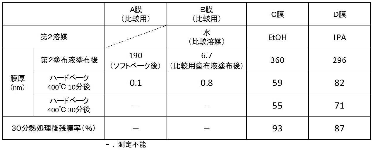
A膜(比較用)のソフトベーク後の膜厚は、便宜上、「第2塗布液塗布後」欄に記載した。
B膜(比較用)の比較用塗布液塗布後の膜厚は、便宜上、「第2塗布液塗布後」欄に記載した。
また、第1塗布液の塗布及びソフトベークを行い、更に、比較溶媒として水を含む比較用塗布液を塗布して得られたB膜(比較用)では、比較用塗布液中の水によって膜が溶解し、比較用塗布液塗布後の段階(即ち、ハードベーク前の段階)で、既に膜厚がわずか6.7nmとなっていた。
これらA膜及びB膜に対し、第1塗布液の塗布及びソフトベークを行い、更に、第2溶媒としてEtOHを含む第2塗布液を塗布して得られたC膜では、第2塗布液の塗布によっても膜が溶解しなかった。寧ろ、第2塗布液の塗布により、第2塗布液の塗布前の膜厚(即ち、A膜のソフトベーク後(便宜上、A膜の「第2塗布液塗布後」欄に記載。以下同じ。)よりも膜厚が上昇した(C膜の第2塗布液塗布後の膜厚参照)。その結果、C膜では、ハードベーク10分後の膜厚が59nmであり、ハードベーク後においても塗膜が十分に残存していた。さらに、30分熱処理後残膜率が93%であり、C膜は十分な耐熱性を有していた。
同様に、第1塗布液の塗布及びソフトベークを行い、更に、第2溶媒としてIPAを含む第2塗布液を塗布して得られたD膜では、第2塗布液の塗布によっても膜が溶解しなかった。寧ろ、第2塗布液の塗布により、第2塗布液の塗布前の膜厚(即ち、A膜のソフトベーク後の膜厚)よりも膜厚が上昇した(D膜の第2塗布液塗布後の膜厚参照)。その結果、D膜では、ハードベーク後の膜厚が82nmであり、ハードベーク後においても塗膜が十分に残存していた。さらに、30分熱処理後残膜率が87%であり、D膜は十分な耐熱性を有していた。
実験例5として、カルボキシル基を2つ以上有する有機物としてのカルボン酸の価数と、膜の耐熱性と、の関係に関する実験を行った(下記表5)。
詳細には、平らなシリコンウエハ表面に、第1塗布液としてのポリエチレンイミン(PEI)塗布液(PEIの重量平均分子量:25000、第1溶媒:水、PEI含有量:3質量%)をスピンコーターで塗布し、次いでソフトベーク(100℃、1min)して塗膜(ソフトベーク後)を得た。
上記得られた塗膜(ソフトベーク後)上に、表5に示すカルボン酸を第2溶媒(EtOH)に溶解させた第2塗布液(カルボン酸含有量:1.5質量%)を塗布し、得られた塗膜の膜厚(ハードベーク前の膜厚)を測定した。次いで、380℃で10分間ハードベークを行い、得られた塗膜の膜厚(ハードベーク後の膜厚)を測定した。
上記で測定されたハードベーク前の膜厚及びハードベーク後の膜厚に基づき、下記式により、ハードベーク後の残膜率(%)を求めた。結果を表5に示す。
ハードベーク後の残膜率(%)=(ハードベーク後の膜の膜厚/ハードベーク前の膜の膜厚)×100
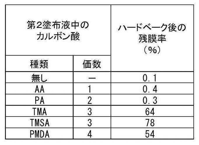
・カルボン酸の種類は以下のとおりである。
AA … 酢酸
PA … フタル酸
TMA … トリメリット酸
TMSA … トリメシン酸
PMDA … ピロメリット酸
・カルボン酸の種類「無し」とは、第2塗布液にカルボン酸を含有させなかったことを示す。
実験例6として、ポリアミンとカルボン酸との反応によるアミド結合及びイミド結合の形成に関する実験を行った。
アミド結合及びイミド結合の形成の確認は、フーリエ変換赤外分光(FT-IR)測定によって行った。
平らなシリコンウエハ表面に、ポリエチレンイミン(PEI)溶液(PEIの重量平均分子量:25000、溶媒:質量比〔エタノール/水〕=1/3の混合溶媒、PEI含有量:3質量%)をスピンコーターで塗布し、次いでソフトベーク(100℃、1min)して、比較用の膜として、E膜を得た。
得られたE膜について、FT-IR測定により、アミド結合及びイミド結合の有無を確認した。
その結果、アミド結合に由来するピークも、イミド結合に由来するピークも、観測されなかった。
平らなシリコンウエハ表面に、ポリエチレンイミン(PEI)及び酢酸の水溶液(PEIの重量平均分子量:25000、溶媒:水、PEI含有量:1.2質量%、酢酸含有量:1.4質量%)をスピンコーターで塗布し、次いでソフトベーク(100℃、1min)して、比較用の膜として、F膜を得た。
得られたF膜について、FT-IR測定により、アミド結合及びイミド結合の有無を確認した。
その結果、アミド結合に由来する弱いピークが観測された。イミド結合に由来するピークは観測されなかった。
上記E膜の表面に、カルボキシル基を2つ以上有する有機物としてのトリメシン酸(TMSA)(3価カルボン酸)を第2溶媒(イソプロピルアルコール)に溶解させた第2塗布液(TMSA含有量:2質量%)を塗布し、次いで、400℃で10分間のハードベークを施し、G膜を得た。
得られたG膜について、FT-IR測定により、アミド結合及びイミド結合の有無を確認した。
その結果、アミド結合に由来する強いピークが観測された。イミド結合に由来するピークは観測されなかった。
上記E膜の表面に、カルボキシル基を2つ以上有する有機物としてのトリメリット酸(TMA)(3価カルボン酸)を第2溶媒(エタノール)に溶解させた第2塗布液(TMA含有量:2質量%)を塗布し、次いで、350℃で2分間のハードベークを施し、H膜を得た。
得られたH膜について、FT-IR測定により、アミド結合及びイミド結合の有無を確認した。
その結果、アミド結合に由来する強いピーク、及び、イミド結合に由来する強いピークが観測された。
埋め込み平坦化膜(特に、金属元素の含有量が金属元素1種類当たり5×10¹⁰atom/cm2以下であること、及び、埋め込み平坦化膜の厚さが100nm以上であることの少なくとも一方を満たす態様の埋め込み平坦化膜)は、後の工程で除去される膜(即ち、犠牲膜)であってもよい。
特に、半導体装置の分野では、いくつかの半導体プロセスの後、埋め込み平坦化膜を除去したいという要求がある。
プラズマ処理として、具体的にはドライエッチングが好ましく、ドライエッチングの中でも、リアクティブイオンエッチングがより好ましい。
埋め込み平坦化膜を除去するためのプラズマ処理については、例えば、特開2011-171572号公報に記載されているドライエッチングの方法を適宜参照することができる。
第2塗布液中のカルボキシル基を2つ以上有する有機物が2価カルボン酸であると、埋め込み平坦化膜を除去性に特に優れる。
実験例7として、UVオゾン処理による埋め込み平坦化膜の除去に関する実験を行った。
平らなシリコンウエハ表面に、ポリエチレンイミン(PEI)塗布液(PEIの重量平均分子量:25000、溶媒:質量比〔エタノール/水〕=1/3、PEI含有量:3質量%)をスピンコーターで塗布し、次いでソフトベーク(100℃、1min)して、塗膜を得た。
得られた塗膜の表面に、トリメリット酸(TMA)(3価カルボン酸)を第2溶媒(エタノール)に溶解させた第2塗布液(TMA含有量:2質量%)を塗布し、次いで、380℃で10分間のハードベークを施し、膜厚100nmのI膜を得た。
得られたI膜に対し、以下の条件で、酸素雰囲気下にてUV照射を行った(UVオゾン処理)。
--UVオゾン処理の条件--
圧力30kPa、O2/N2=20(cm3/min.)/600(cm3/min.)、400℃、30min、UV(λ=172nm,14mW/cm2)
上述したI膜の作製において、トリメリット酸(TMA)(3価カルボン酸)を第2溶媒(エタノール)に溶解させた第2塗布液(TMA含有量:2質量%)を、1,2,3-プロパントリカルボン酸(1,2,3-PTCA)(3価カルボン酸)を第2溶媒(イソプロピルアルコール)に溶解させた第2塗布液(1,2,3-PTCA含有量:2質量%)に変更したこと以外はI膜の作製と同様にして、膜厚40nmのJ膜を得た。
実験例8として、カルボキシル基を2つ以上有する有機物としてフタル酸(2価カルボン酸)を用いた埋め込み平坦化膜を、加熱処理によって除去する実験を行った。
平らなシリコンウエハ表面に、ポリエチレンイミン(PEI)及びフタル酸(PA)を溶媒に溶解させた溶液(PEIの重量平均分子量:25000、溶媒:質量比〔エタノール/水〕=1/3、PEI含有量:1.5質量%、PA含有量:2質量%)をスピンコーターで塗布し、次いでソフトベーク(100℃、1min)して、膜厚66.1nmのK膜を得た。
平らなシリコンウエハ表面に、ポリエチレンイミン(PEI)溶液(PEIの重量平均分子量:25000、溶媒:質量比〔エタノール/水〕=1/3、PEI含有量:1.5質量%)をスピンコーターで塗布し、次いでソフトベーク(100℃、1min)して、塗膜を得た。
得られた塗膜の表面に、フタル酸(PA)を第2溶媒(エタノール)に溶解させた第2塗布液(PA含有量:2質量%)を塗布し、膜厚113.9nmのL膜を得た。
上記K膜及びL膜の各々に対し、380℃で30分間の加熱除去処理を施した。
ソフトベーク後の膜厚と加熱除去処理後の膜厚から、下記式により、加熱除去処理後の残膜率を求めた。
加熱処理後の残膜率(%)=(加熱処理後の膜の膜厚/ソフトベーク後の膜の膜厚)×100
その結果、K膜の加熱除去処理後の残膜率はわずか0.5%であり、加熱除去処理によってK膜がほぼ除去されていた。
L膜の加熱除去処理後の残膜率はわずか0.5%であり、加熱除去処理によってL膜がほぼ除去されていた。
実験例9として、深さ方向についてポリアミンとカルボン酸との反応によるアミド結合の形成に関する実験を行った。
深さ方向のアミド結合の形成の確認は、飛行時間型二次イオン質量分析法(TOF-SIMS:Time of Flight - Secondary Ion Mass Spectrometry)によって行った。TOF-SIMS測定は、「TOF.SIMS 5」(ION-TOF社製)で行った。
平らなシリコンウエハ表面に、ポリエチレンイミン(PEI)の水溶液(PEIの重量平均分子量:25000、溶媒:水、PEI含有量:3質量%)をスピンコーターで塗布し、次いでソフトベーク(100℃、1min)し、塗膜を得た。
得られた塗膜の表面に、カルボキシル基を2つ以上有する有機物としてのトリメシン酸(TMSA)(3価カルボン酸)を第2溶媒(イソプロピルアルコール)に溶解させた第2塗布液(TMSA含有量:2質量%)を塗布し、次いで、400℃で10分間のハードベークを施し、M膜を得た。
得られたM膜について、TOF-SIMS測定により、深さ方向でのアミド結合の有無を確認した。
図2中、横軸は測定対象の深さ(Depth)(単位:nm)を表し、縦軸は、2次イオンの規格化強度(Normalized Intensity)を示す。
図2中、深さ0nmの地点はM膜の表面を示し、深さ0nm~100nmの領域はM膜(M-film)を示し、深さ100nmより深い領域は、シリコンウエハ(Si-sub.)を示す。
図2中、
「C_2H-」は、有機物全般に由来する2次イオンの強度であり、
「CN-」及び「13CN-」は、窒素を含む有機物全般に由来する2次イオンの強度であり、
「CNO-」は、アミド等に由来する2次イオンの強度であり、
「C_7H_4NO-」は、芳香族アミド等に由来する2次イオンの強度であり、
「O-」は、酸素に由来する2次イオンの強度であり、
「Si-」及び「SiO_3-」は、シリコン及びシリコン酸化物に由来する2次イオンの強度である。
TOF-SIMSの結果から、第2塗布液のカルボキシル基を2つ以上有する有機物は、第1塗布液の塗膜表面だけでなく、塗膜全体で反応していることがわかった。
本実施形態の電子デバイスの製造方法は、前述した本実施形態の埋め込み平坦化膜の製造方法により、前記凹部を有する部材である半導体基板又は回路基板に対し、前記埋め込み平坦化膜を形成する埋め込み平坦化膜形成工程を有する。
本実施形態の電子デバイスの製造方法により、電子デバイスとして、半導体装置又は回路基板が製造される。この電子デバイスは、凹部に対する充填性(埋め込み性)に優れ、耐熱性に優れた埋め込み平坦化膜を備える。
埋め込み平坦化膜は、更に、プラズマ耐性にも優れる。
その他の工程としては、半導体プロセスや回路基板プロセスにおける公知の工程が挙げられる。
例えば、本実施形態の電子デバイスの製造方法は、その他の工程として、プラズマ工程を有していてもよい。
プラズマ工程におけるプラズマとしては、ヘリウムガス、アルゴンガス、窒素ガス、アンモニアガス、及びフルオロカーボン系ガスからなる群から選択される少なくとも1種のガスから発生したプラズマが挙げられる。
本実施形態の電子デバイスの製造方法が、プラズマ工程を有する場合であっても、プラズマによる埋め込み平坦化膜のダメージが低減される。
除去工程における埋め込み平坦化膜の除去方法としては、前述したUVオゾン処理、又は、埋め込み平坦化膜の除去処理としてのプラズマ処理が挙げられる。
また、カルボキシル基を2つ以上有する有機物として2価カルボン酸を用いた場合には、除去方法は、埋め込み平坦化膜が形成された半導体装置又は回路基板を380℃以上に加熱する方法であってもよい。
<凹部を有する部材の準備>
凹部を有する部材として、溝(アスペクト比3.6、幅50nm、深さ180nm)が形成されたシリコンウエハ1を準備した。
ポリアミンであるポリエチレンイミン(PEI、BASF社製、銘柄:Rupasol WF、重量平均分子量:25000)を、第1溶媒としての水に溶解させた塗布液a1(第1塗布液)(PEI含有量:3質量%、pH(25℃)10.5)を準備した。
トリメシン酸(TMSA)(3価カルボン酸)(Aldrich社製)を、第2溶媒としてのイソプロピルアルコール(IPA;和光純薬製SCグレード)に溶解させた塗布液a2(第2塗布液)(TMSA含有量:1.5質量%)を準備した。
上記シリコンウエハ1をスピンコーター(ABLE Co. Ltd.製)に載置し、上記シリコンウエハ1の溝形成面に、塗布液a1(第1塗布液)をピペットを使用して、1mL吐出した後、回転数1000rpmで1秒間、さらに回転数600rpmで60秒間回転させて乾燥塗膜を得た。次いで、ホットプレート上で空気中でソフトベーク(100℃、1min)して、塗膜(ソフトベーク後)を得た。塗膜(ソフトベーク後)が形成されたシリコンウエハを、以下、「塗膜形成シリコンウエハ」ともいう。
第1塗布工程で得られた上記塗膜形成シリコンウエハをスピンコーターに載置し、塗膜形成シリコンウエハの塗膜の表面に、塗布液a2(第2塗布液)を1mL吐出し、回転数1000rpmで1秒間、さらに回転数600rpmで60秒間回転して乾燥し、塗膜(第2塗布液塗布後)を得た。得られた塗膜(第2塗布液塗布後)に対し、ホットプレート(アペックス社製SPX-1120)を用いて、窒素中にて、圧力30kPa、400℃で30分間のハードベークを施した。
以上により、埋め込み平坦化膜(図1中の埋め込み平坦化膜100)を得た。
得られたSEM写真を図1に示す。
図1中、「Si」はシリコンウエハを示し、「100」は埋め込み平坦化膜を示す。
図1に示すように、溝の内部に、埋め込み平坦化膜100がボイドを生じることなく充填されていることがわかった。
<凹部を有する部材の準備>
凹部を有する部材として、溝(アスペクト比0.67、幅180nm、深さ120nm)が形成されたシリコンウエハ2を準備した。
シリコンウエハ2は、SiO2膜付きシリコンウエハである。
詳細には、シリコンウエハ上にプラズマCVDによってSiO2膜を形成し、次いでフォトリソグラフィー及びドライエッチングにより、SiO2膜の一部を除去することにより、上記溝を形成した。これによりシリコンウエハ2を得た。
ピロメリット酸(PMDA)(4価カルボン酸)(ロンザ社製)を、第2溶媒としてのエタノール(EtOH;和光純薬製SCグレード)に溶解させた塗布液b2(第2塗布液)(PMDA含有量:2.5質量%)を準備した。
上記シリコンウエハ1に代えて上記シリコンウエハ2を用いたこと以外は実施例1の第1塗布工程と同様にして、塗膜形成シリコンウエハを得た。
第1塗布工程で得られた上記塗膜形成シリコンウエハの表面に、第2塗布液b2を用いて実施例1の第2塗布工程と同様にして塗膜(第2塗布液塗布後)を得た。得られた塗膜(第2塗布液塗布後)に対し、温度を380℃に変更したこと以外は実施例1と同様にしてハードベークを施した。
以上で製造した埋め込み平坦化膜付きのシリコンウエハの断面を、透過型電子顕微鏡(TEM)にて観察し、TEM写真(倍率100000倍)を撮影した。
得られたTEM写真を図3に示す。
図3中、「Si」はシリコンウエハを示し、「SiO2」はSiO2膜を示し、「100」は埋め込み平坦化膜を示す。
図3に示すように、溝の内部に、埋め込み平坦化膜100がボイドを生じることなく充填されていることがわかった。
<凹部を有する部材の準備>
凹部を有する部材として、溝(アスペクト比2、幅100nm、深さ200nm)が形成されたシリコンウエハ3を準備した。
無水フタル酸(PA)(2価カルボン酸)(Aldrich社製)を、第2溶媒としてのイソプロピルアルコール(IPA;和光純薬製SCグレード)に溶解させた塗布液c2(第2塗布液)(PA含有量:3.0質量%)を準備した。
上記シリコンウエハ1に代えて上記シリコンウエハ3を用いたこと以外は実施例1の第1塗布工程と同様にして、塗膜形成シリコンウエハを得た。
第1塗布工程で得られた上記塗膜形成シリコンウエハの表面に、第2塗布液c2を用いて実施例1の第2塗布工程と同様にして塗膜(第2塗布液塗布後)を得た。
得られた塗膜(第2塗布液塗布後)に対し、ホットプレート(アペックス社製SPX-1120)を用いて、窒素中にて、圧力30kPa、350℃で40分間のハードベークを施した。
以上で製造した埋め込み平坦化膜付きのシリコンウエハの断面を、走査型電子顕微鏡(SEM)にて観察し、SEM写真(倍率150000倍)を撮影した。
図4中、「Si」はシリコンウエハを示し、「100」は埋め込み平坦化膜を示す。
図4に示すように、溝の内部に、埋め込み平坦化膜100がボイドを生じることなく充填されていることがわかった。
<塗布液b2(第2塗布液)の準備>
無水ピロメリット酸(PMDA)(4価カルボン酸)(ロンザ社製)を、第2溶媒としてのエタノール(EtOH;和光純薬製SCグレード)に溶解させた塗布液d2(第2塗布液)(PMDA含有量:2.0質量%)を準備した。
上記シリコンウエハ1に代えて上記シリコンウエハ3を用いたこと以外は実施例1の第1塗布工程と同様にして、塗膜形成シリコンウエハを得た。
第1塗布工程で得られた上記塗膜形成シリコンウエハの表面に、第2塗布液d2を用いて実施例1の第2塗布工程と同様にして塗膜(第2塗布液塗布後)を得た。
得られた塗膜(第2塗布液塗布後)に対し、ホットプレート(アペックス社製SPX-1120)を用いて、窒素中にて、圧力30kPa、400℃で10分間のハードベークを施した。
以上で製造した埋め込み平坦化膜付きのシリコンウエハの断面を、走査型電子顕微鏡(SEM)にて観察し、SEM写真(倍率150000倍)を撮影した。
得られたSEM写真を図5に示す。
図5中、「Si」はシリコンウエハを示し、「100」は埋め込み平坦化膜を示す。
図5に示すように、溝の内部に、埋め込み平坦化膜100がボイドを生じることなく充填されていることがわかった。なお、図5の埋め込み平坦化膜100中の粒状物は、SEM観察用サンプル作製時に埋め込み平坦化膜100の断面にできた凹凸である。
上記シリコンウエハ1に代えて上記シリコンウエハ3を用いたこと以外は実施例1の第1塗布工程と同様にして、塗膜形成シリコンウエハを得た。
上記塗膜形成シリコンウエハの塗膜に対する第2塗布液の塗布を行うことなく、上記塗膜形成シリコンウエハに対し、ホットプレート(アペックス社製SPX-1120)を用いて、窒素中にて、圧力30kPa、350℃で30分間のハードベークを施した。以上により、比較膜付きシリコンウエハを得た。
以上で製造した比較膜付きのシリコンウエハの断面を、走査型電子顕微鏡(SEM)にて観察し、SEM写真(倍率150000倍)を撮影した。
得られたSEM写真を図6に示す。
図6中、「Si」はシリコンウエハを示し、「101」は比較膜を示し、「102」は、溝の上部の空隙を示す。
図6に示すように、溝の内部が比較膜101で充填されておらず、溝の上部に空隙102が生じていることがわかった。
350℃で10分間熱処理した膜の膜厚に対する30分間熱処理した膜の膜厚は16%であった。
この結果は、第1塗布液のポリアミンが350℃のハードベークにより収縮したことを示すと考えられる。
以上の結果から、カルボキシル基を2つ以上有する有機物と反応していないポリアミンのみからなる膜(例えば、上記比較膜)は、耐熱性が不足することがわかった。
本明細書に記載された全ての文献、特許出願、及び技術規格は、個々の文献、特許出願、及び技術規格が参照により取り込まれることが具体的かつ個々に記された場合と同程度に、本明細書中に参照により取り込まれる。
Claims (9)
- 凹部を有する部材の前記凹部を含む領域に、ポリアミン及び第1溶媒を含む第1塗布液を塗布して前記凹部に前記第1塗布液を埋め込む第1塗布工程と、
前記部材の前記第1塗布液が埋め込まれた前記凹部を含む領域に、カルボキシル基を2つ以上有する有機物及び沸点が200℃以下でありSP値が30(MPa)1/2以下である第2溶媒を含む第2塗布液を塗布することにより、前記部材の前記凹部を含む領域を平坦化させる埋め込み平坦化膜を形成する第2塗布工程と、
を有する、埋め込み平坦化膜の製造方法。 - 前記カルボキシル基を2つ以上有する有機物が、2価以上のカルボン酸である、請求項1に記載の埋め込み平坦化膜の製造方法。
- 前記第1塗布液中の前記ポリアミンの含有量が、1.0質量%以上20質量%以下である、請求項1又は請求項2に記載の埋め込み平坦化膜の製造方法。
- 前記第1溶媒は、沸点が200℃以下であり、親水性である、請求項1~請求項3のいずれか1項に記載の埋め込み平坦化膜の製造方法。
- 前記埋め込み平坦化膜がアミド結合を有する、請求項1~請求項4のいずれか1項に記載の埋め込み平坦化膜の製造方法。
- 前記凹部は、幅が250nm以下であり、幅に対する深さの比〔深さ/幅〕が0.3以上である、請求項1~請求項5のいずれか1項に記載の埋め込み平坦化膜の製造方法。
- 前記埋め込み平坦化膜中の金属元素の単位面積当たりの含有量が、金属元素1種類当たり、5×10¹⁰atom/cm2以下である、請求項1~請求項6のいずれか1項に記載の埋め込み平坦化膜の製造方法。
- 請求項1~請求項7のいずれか1項に記載の埋め込み平坦化膜の製造方法により、前記凹部を有する部材である半導体基板又は回路基板に対し、前記埋め込み平坦化膜を形成する埋め込み平坦化膜形成工程を有する、電子デバイスの製造方法。
- 更に、前記埋め込み平坦化膜を除去する除去工程を有する、請求項8に記載の電子デバイスの製造方法。
Priority Applications (6)
| Application Number | Priority Date | Filing Date | Title |
|---|---|---|---|
| US15/562,072 US10043677B2 (en) | 2015-03-30 | 2016-03-24 | Method for manufacturing filling planarization film and method for manufacturing electronic device |
| KR1020177027404A KR101926294B1 (ko) | 2015-03-30 | 2016-03-24 | 매입 평탄화막의 제조 방법 및 전자 디바이스의 제조 방법 |
| CN201680018934.5A CN107431016A (zh) | 2015-03-30 | 2016-03-24 | 填埋平坦化膜的制造方法及电子器件的制造方法 |
| JP2017509879A JP6364544B2 (ja) | 2015-03-30 | 2016-03-24 | 埋め込み平坦化膜の製造方法及び電子デバイスの製造方法 |
| SG11201707977PA SG11201707977PA (en) | 2015-03-30 | 2016-03-24 | Method for manufacturing filling planarization film and method for manufacturing electronic device |
| IL254702A IL254702A0 (en) | 2015-03-30 | 2017-09-26 | Method for manufacturing filling planarization film and method for manufacturing electronic device |
Applications Claiming Priority (2)
| Application Number | Priority Date | Filing Date | Title |
|---|---|---|---|
| JP2015-069833 | 2015-03-30 | ||
| JP2015069833 | 2015-03-30 |
Publications (1)
| Publication Number | Publication Date |
|---|---|
| WO2016158697A1 true WO2016158697A1 (ja) | 2016-10-06 |
Family
ID=57004654
Family Applications (1)
| Application Number | Title | Priority Date | Filing Date |
|---|---|---|---|
| PCT/JP2016/059482 Ceased WO2016158697A1 (ja) | 2015-03-30 | 2016-03-24 | 埋め込み平坦化膜の製造方法及び電子デバイスの製造方法 |
Country Status (8)
| Country | Link |
|---|---|
| US (1) | US10043677B2 (ja) |
| JP (1) | JP6364544B2 (ja) |
| KR (1) | KR101926294B1 (ja) |
| CN (1) | CN107431016A (ja) |
| IL (1) | IL254702A0 (ja) |
| SG (1) | SG11201707977PA (ja) |
| TW (1) | TWI664677B (ja) |
| WO (1) | WO2016158697A1 (ja) |
Cited By (1)
| Publication number | Priority date | Publication date | Assignee | Title |
|---|---|---|---|---|
| JP2020080394A (ja) * | 2018-11-14 | 2020-05-28 | 東京エレクトロン株式会社 | 半導体メモリの製造方法 |
Families Citing this family (2)
| Publication number | Priority date | Publication date | Assignee | Title |
|---|---|---|---|---|
| CN107731872B (zh) | 2017-09-30 | 2021-11-02 | 京东方科技集团股份有限公司 | 一种基板及其制备方法、显示面板、显示装置 |
| CN112382647B (zh) * | 2020-11-10 | 2022-05-24 | 合肥鑫晟光电科技有限公司 | 显示基板及其制备方法、显示面板、显示装置 |
Citations (4)
| Publication number | Priority date | Publication date | Assignee | Title |
|---|---|---|---|---|
| JP2003021827A (ja) * | 2001-07-10 | 2003-01-24 | Nec Kagoshima Ltd | 有機膜の平坦化方法及びそれを用いた液晶表示装置の製造方法 |
| JP2007266264A (ja) * | 2006-03-28 | 2007-10-11 | Fujitsu Ltd | 半導体装置の製造方法 |
| JP2011082236A (ja) * | 2009-10-05 | 2011-04-21 | Nissan Chem Ind Ltd | 半導体基板の平坦化方法 |
| WO2014013956A1 (ja) * | 2012-07-17 | 2014-01-23 | 三井化学株式会社 | 半導体装置及びその製造方法並びにリンス液 |
Family Cites Families (13)
| Publication number | Priority date | Publication date | Assignee | Title |
|---|---|---|---|---|
| DE2118690A1 (de) * | 1971-04-17 | 1973-02-01 | Reichhold Albert Chemie Ag | Verfahren zur herstellung von polyimiden |
| DE4335323A1 (de) * | 1993-10-18 | 1995-04-20 | Basf Lacke & Farben | Lösungen von polyimidbildenden Substanzen und deren Verwendung |
| US5435888A (en) * | 1993-12-06 | 1995-07-25 | Sgs-Thomson Microelectronics, Inc. | Enhanced planarization technique for an integrated circuit |
| US5716677A (en) * | 1996-03-21 | 1998-02-10 | Ohio Aerospace Institute | Protective coatings for polyimide composites |
| JP2953447B2 (ja) | 1997-11-14 | 1999-09-27 | 日本電気株式会社 | 溝分離型半導体装置の製造方法 |
| US6333274B2 (en) * | 1998-03-31 | 2001-12-25 | Kabushiki Kaisha Toshiba | Method of manufacturing a semiconductor device including a seamless shallow trench isolation step |
| JP4654544B2 (ja) * | 2000-07-12 | 2011-03-23 | 日産化学工業株式会社 | リソグラフィー用ギャップフィル材形成組成物 |
| WO2002059176A1 (fr) * | 2001-01-25 | 2002-08-01 | Sanyo Chemical Industries, Ltd | Resine durcissable, matiere resineuse durcissable, pellicule durcissable et isolant electrique |
| KR100428806B1 (ko) * | 2001-07-03 | 2004-04-28 | 삼성전자주식회사 | 트렌치 소자분리 구조체 및 그 형성 방법 |
| US20030125869A1 (en) | 2002-01-02 | 2003-07-03 | International Business Machines Corporation | Method and apparatus for creating a geographically limited vocabulary for a speech recognition system |
| AU2004255334A1 (en) * | 2003-07-14 | 2005-01-20 | Cytec Surface Specialties, S.A. | Waterbone self-crosslinkable polyurethane dispersions and polyurethane: acrylic hybrid dispersions |
| JP4507629B2 (ja) * | 2004-02-20 | 2010-07-21 | 東洋インキ製造株式会社 | 樹脂グラフトカーボンブラック組成物 |
| JP2007313475A (ja) * | 2006-05-29 | 2007-12-06 | Basf Coatings Japan Ltd | 複層塗膜形成方法およびその塗装物品 |
-
2016
- 2016-03-24 KR KR1020177027404A patent/KR101926294B1/ko not_active Expired - Fee Related
- 2016-03-24 JP JP2017509879A patent/JP6364544B2/ja not_active Expired - Fee Related
- 2016-03-24 US US15/562,072 patent/US10043677B2/en not_active Expired - Fee Related
- 2016-03-24 CN CN201680018934.5A patent/CN107431016A/zh active Pending
- 2016-03-24 SG SG11201707977PA patent/SG11201707977PA/en unknown
- 2016-03-24 WO PCT/JP2016/059482 patent/WO2016158697A1/ja not_active Ceased
- 2016-03-25 TW TW105109386A patent/TWI664677B/zh not_active IP Right Cessation
-
2017
- 2017-09-26 IL IL254702A patent/IL254702A0/en unknown
Patent Citations (4)
| Publication number | Priority date | Publication date | Assignee | Title |
|---|---|---|---|---|
| JP2003021827A (ja) * | 2001-07-10 | 2003-01-24 | Nec Kagoshima Ltd | 有機膜の平坦化方法及びそれを用いた液晶表示装置の製造方法 |
| JP2007266264A (ja) * | 2006-03-28 | 2007-10-11 | Fujitsu Ltd | 半導体装置の製造方法 |
| JP2011082236A (ja) * | 2009-10-05 | 2011-04-21 | Nissan Chem Ind Ltd | 半導体基板の平坦化方法 |
| WO2014013956A1 (ja) * | 2012-07-17 | 2014-01-23 | 三井化学株式会社 | 半導体装置及びその製造方法並びにリンス液 |
Cited By (2)
| Publication number | Priority date | Publication date | Assignee | Title |
|---|---|---|---|---|
| JP2020080394A (ja) * | 2018-11-14 | 2020-05-28 | 東京エレクトロン株式会社 | 半導体メモリの製造方法 |
| JP7154114B2 (ja) | 2018-11-14 | 2022-10-17 | 東京エレクトロン株式会社 | 半導体メモリの製造方法 |
Also Published As
| Publication number | Publication date |
|---|---|
| SG11201707977PA (en) | 2017-10-30 |
| KR101926294B1 (ko) | 2018-12-06 |
| KR20170121264A (ko) | 2017-11-01 |
| JPWO2016158697A1 (ja) | 2017-09-28 |
| US20180076047A1 (en) | 2018-03-15 |
| IL254702A0 (en) | 2017-11-30 |
| US10043677B2 (en) | 2018-08-07 |
| TW201707088A (zh) | 2017-02-16 |
| CN107431016A (zh) | 2017-12-01 |
| TWI664677B (zh) | 2019-07-01 |
| JP6364544B2 (ja) | 2018-07-25 |
Similar Documents
| Publication | Publication Date | Title |
|---|---|---|
| TWI602246B (zh) | 半導體裝置及其製造方法及清洗液 | |
| EP2164648B1 (en) | Low k dielectric | |
| KR102075905B1 (ko) | 반도체용 막 조성물, 반도체용 막 조성물의 제조 방법, 반도체용 부재의 제조 방법, 반도체용 공정재의 제조 방법 및 반도체 장치 | |
| JP6364544B2 (ja) | 埋め込み平坦化膜の製造方法及び電子デバイスの製造方法 | |
| CN105051872B (zh) | 复合体的制造方法及组合物 | |
| WO2016017678A1 (ja) | 犠牲膜用組成物、およびその製造方法、ならびにその組成物を用いて形成された空隙を具備した半導体装置、およびその組成物を用いた半導体装置の製造方法 | |
| WO2020067467A1 (ja) | 平坦化膜形成用塗布液、平坦化膜形成用塗布液の製造方法、平坦化膜付き金属箔、及び平坦化膜付き金属箔の製造方法 | |
| CN107004599B (zh) | 基板中间体、贯通通孔电极基板及贯通通孔电极形成方法 | |
| US10580639B2 (en) | Sealing composition and method of manufacturing semiconductor device | |
| JP2004253626A (ja) | 多孔性絶縁膜、電子装置及びそれらの製造方法 | |
| JP2011040634A (ja) | 多孔質膜の前駆体組成物、多孔質膜及びその作製方法、並びに半導体装置 |
Legal Events
| Date | Code | Title | Description |
|---|---|---|---|
| 121 | Ep: the epo has been informed by wipo that ep was designated in this application |
Ref document number: 16772578 Country of ref document: EP Kind code of ref document: A1 |
|
| ENP | Entry into the national phase |
Ref document number: 2017509879 Country of ref document: JP Kind code of ref document: A |
|
| WWE | Wipo information: entry into national phase |
Ref document number: 254702 Country of ref document: IL |
|
| ENP | Entry into the national phase |
Ref document number: 20177027404 Country of ref document: KR Kind code of ref document: A |
|
| WWE | Wipo information: entry into national phase |
Ref document number: 15562072 Country of ref document: US |
|
| WWE | Wipo information: entry into national phase |
Ref document number: 11201707977P Country of ref document: SG |
|
| NENP | Non-entry into the national phase |
Ref country code: DE |
|
| 122 | Ep: pct application non-entry in european phase |
Ref document number: 16772578 Country of ref document: EP Kind code of ref document: A1 |