WO2016158089A1 - 蛍光光源装置 - Google Patents
蛍光光源装置 Download PDFInfo
- Publication number
- WO2016158089A1 WO2016158089A1 PCT/JP2016/055163 JP2016055163W WO2016158089A1 WO 2016158089 A1 WO2016158089 A1 WO 2016158089A1 JP 2016055163 W JP2016055163 W JP 2016055163W WO 2016158089 A1 WO2016158089 A1 WO 2016158089A1
- Authority
- WO
- WIPO (PCT)
- Prior art keywords
- layer
- fluorescent
- light source
- source device
- fluorescent plate
- Prior art date
- Legal status (The legal status is an assumption and is not a legal conclusion. Google has not performed a legal analysis and makes no representation as to the accuracy of the status listed.)
- Ceased
Links
Images

Classifications
-
- F—MECHANICAL ENGINEERING; LIGHTING; HEATING; WEAPONS; BLASTING
- F21—LIGHTING
- F21V—FUNCTIONAL FEATURES OR DETAILS OF LIGHTING DEVICES OR SYSTEMS THEREOF; STRUCTURAL COMBINATIONS OF LIGHTING DEVICES WITH OTHER ARTICLES, NOT OTHERWISE PROVIDED FOR
- F21V7/00—Reflectors for light sources
- F21V7/22—Reflectors for light sources characterised by materials, surface treatments or coatings, e.g. dichroic reflectors
-
- C—CHEMISTRY; METALLURGY
- C23—COATING METALLIC MATERIAL; COATING MATERIAL WITH METALLIC MATERIAL; CHEMICAL SURFACE TREATMENT; DIFFUSION TREATMENT OF METALLIC MATERIAL; COATING BY VACUUM EVAPORATION, BY SPUTTERING, BY ION IMPLANTATION OR BY CHEMICAL VAPOUR DEPOSITION, IN GENERAL; INHIBITING CORROSION OF METALLIC MATERIAL OR INCRUSTATION IN GENERAL
- C23C—COATING METALLIC MATERIAL; COATING MATERIAL WITH METALLIC MATERIAL; SURFACE TREATMENT OF METALLIC MATERIAL BY DIFFUSION INTO THE SURFACE, BY CHEMICAL CONVERSION OR SUBSTITUTION; COATING BY VACUUM EVAPORATION, BY SPUTTERING, BY ION IMPLANTATION OR BY CHEMICAL VAPOUR DEPOSITION, IN GENERAL
- C23C14/00—Coating by vacuum evaporation, by sputtering or by ion implantation of the coating forming material
- C23C14/06—Coating by vacuum evaporation, by sputtering or by ion implantation of the coating forming material characterised by the coating material
- C23C14/14—Metallic material, boron or silicon
- C23C14/16—Metallic material, boron or silicon on metallic substrates or on substrates of boron or silicon
-
- C—CHEMISTRY; METALLURGY
- C23—COATING METALLIC MATERIAL; COATING MATERIAL WITH METALLIC MATERIAL; CHEMICAL SURFACE TREATMENT; DIFFUSION TREATMENT OF METALLIC MATERIAL; COATING BY VACUUM EVAPORATION, BY SPUTTERING, BY ION IMPLANTATION OR BY CHEMICAL VAPOUR DEPOSITION, IN GENERAL; INHIBITING CORROSION OF METALLIC MATERIAL OR INCRUSTATION IN GENERAL
- C23C—COATING METALLIC MATERIAL; COATING MATERIAL WITH METALLIC MATERIAL; SURFACE TREATMENT OF METALLIC MATERIAL BY DIFFUSION INTO THE SURFACE, BY CHEMICAL CONVERSION OR SUBSTITUTION; COATING BY VACUUM EVAPORATION, BY SPUTTERING, BY ION IMPLANTATION OR BY CHEMICAL VAPOUR DEPOSITION, IN GENERAL
- C23C14/00—Coating by vacuum evaporation, by sputtering or by ion implantation of the coating forming material
- C23C14/22—Coating by vacuum evaporation, by sputtering or by ion implantation of the coating forming material characterised by the process of coating
- C23C14/24—Vacuum evaporation
- C23C14/28—Vacuum evaporation by wave energy or particle radiation
- C23C14/30—Vacuum evaporation by wave energy or particle radiation by electron bombardment
-
- C—CHEMISTRY; METALLURGY
- C23—COATING METALLIC MATERIAL; COATING MATERIAL WITH METALLIC MATERIAL; CHEMICAL SURFACE TREATMENT; DIFFUSION TREATMENT OF METALLIC MATERIAL; COATING BY VACUUM EVAPORATION, BY SPUTTERING, BY ION IMPLANTATION OR BY CHEMICAL VAPOUR DEPOSITION, IN GENERAL; INHIBITING CORROSION OF METALLIC MATERIAL OR INCRUSTATION IN GENERAL
- C23C—COATING METALLIC MATERIAL; COATING MATERIAL WITH METALLIC MATERIAL; SURFACE TREATMENT OF METALLIC MATERIAL BY DIFFUSION INTO THE SURFACE, BY CHEMICAL CONVERSION OR SUBSTITUTION; COATING BY VACUUM EVAPORATION, BY SPUTTERING, BY ION IMPLANTATION OR BY CHEMICAL VAPOUR DEPOSITION, IN GENERAL
- C23C14/00—Coating by vacuum evaporation, by sputtering or by ion implantation of the coating forming material
- C23C14/22—Coating by vacuum evaporation, by sputtering or by ion implantation of the coating forming material characterised by the process of coating
- C23C14/34—Sputtering
-
- F—MECHANICAL ENGINEERING; LIGHTING; HEATING; WEAPONS; BLASTING
- F21—LIGHTING
- F21K—NON-ELECTRIC LIGHT SOURCES USING LUMINESCENCE; LIGHT SOURCES USING ELECTROCHEMILUMINESCENCE; LIGHT SOURCES USING CHARGES OF COMBUSTIBLE MATERIAL; LIGHT SOURCES USING SEMICONDUCTOR DEVICES AS LIGHT-GENERATING ELEMENTS; LIGHT SOURCES NOT OTHERWISE PROVIDED FOR
- F21K9/00—Light sources using semiconductor devices as light-generating elements, e.g. using light-emitting diodes [LED] or lasers
-
- F—MECHANICAL ENGINEERING; LIGHTING; HEATING; WEAPONS; BLASTING
- F21—LIGHTING
- F21K—NON-ELECTRIC LIGHT SOURCES USING LUMINESCENCE; LIGHT SOURCES USING ELECTROCHEMILUMINESCENCE; LIGHT SOURCES USING CHARGES OF COMBUSTIBLE MATERIAL; LIGHT SOURCES USING SEMICONDUCTOR DEVICES AS LIGHT-GENERATING ELEMENTS; LIGHT SOURCES NOT OTHERWISE PROVIDED FOR
- F21K9/00—Light sources using semiconductor devices as light-generating elements, e.g. using light-emitting diodes [LED] or lasers
- F21K9/60—Optical arrangements integrated in the light source, e.g. for improving the colour rendering index or the light extraction
- F21K9/64—Optical arrangements integrated in the light source, e.g. for improving the colour rendering index or the light extraction using wavelength conversion means distinct or spaced from the light-generating element, e.g. a remote phosphor layer
-
- F—MECHANICAL ENGINEERING; LIGHTING; HEATING; WEAPONS; BLASTING
- F21—LIGHTING
- F21V—FUNCTIONAL FEATURES OR DETAILS OF LIGHTING DEVICES OR SYSTEMS THEREOF; STRUCTURAL COMBINATIONS OF LIGHTING DEVICES WITH OTHER ARTICLES, NOT OTHERWISE PROVIDED FOR
- F21V29/00—Protecting lighting devices from thermal damage; Cooling or heating arrangements specially adapted for lighting devices or systems
- F21V29/50—Cooling arrangements
- F21V29/502—Cooling arrangements characterised by the adaptation for cooling of specific components
- F21V29/505—Cooling arrangements characterised by the adaptation for cooling of specific components of reflectors
-
- F—MECHANICAL ENGINEERING; LIGHTING; HEATING; WEAPONS; BLASTING
- F21—LIGHTING
- F21V—FUNCTIONAL FEATURES OR DETAILS OF LIGHTING DEVICES OR SYSTEMS THEREOF; STRUCTURAL COMBINATIONS OF LIGHTING DEVICES WITH OTHER ARTICLES, NOT OTHERWISE PROVIDED FOR
- F21V7/00—Reflectors for light sources
- F21V7/22—Reflectors for light sources characterised by materials, surface treatments or coatings, e.g. dichroic reflectors
- F21V7/24—Reflectors for light sources characterised by materials, surface treatments or coatings, e.g. dichroic reflectors characterised by the material
- F21V7/26—Reflectors for light sources characterised by materials, surface treatments or coatings, e.g. dichroic reflectors characterised by the material the material comprising photoluminescent substances
-
- F—MECHANICAL ENGINEERING; LIGHTING; HEATING; WEAPONS; BLASTING
- F21—LIGHTING
- F21V—FUNCTIONAL FEATURES OR DETAILS OF LIGHTING DEVICES OR SYSTEMS THEREOF; STRUCTURAL COMBINATIONS OF LIGHTING DEVICES WITH OTHER ARTICLES, NOT OTHERWISE PROVIDED FOR
- F21V9/00—Elements for modifying spectral properties, polarisation or intensity of the light emitted, e.g. filters
- F21V9/30—Elements containing photoluminescent material distinct from or spaced from the light source
Definitions
- the present invention relates to a fluorescent light source device.
- a fluorescent light source device having a configuration in which laser light is irradiated onto a fluorescent plate as excitation light and fluorescence is emitted from the fluorescent plate.
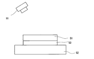
- a certain type of such a fluorescent light source device contains a phosphor that emits fluorescence by excitation light from an excitation light source 11 such as a semiconductor laser, and has a surface (FIG. 4).
- the fluorescent plate 51 has a reflective function on the back surface by providing a reflective layer.
- the reflective layer is preferably made of a metal having high light reflection characteristics, and aluminum (Al), silver (Ag), or the like is used as the metal constituting the reflective layer.
- a bonding member layer 53 made of metal such as solder is interposed between the reflective layer provided on the fluorescent plate 51 and the heat dissipation substrate 52, and the fluorescent plate 51 is placed on the heat dissipation substrate 52 by the bonding member layer 53. Are joined.
- the reflectance of the reflective layer is reduced due to surface degradation due to oxidation and sulfurization.
- the bonded portion becomes high temperature, so that the low reflectance material contained in the bonding member diffuses into the reflective layer.
- the reflectance decreases.
- the problem of a decrease in the reflectance of the reflective layer due to such surface deterioration and diffusion of the metal contained in the joining member is that the protection layer for weather resistance and the diffusion of substances contained in the joining member are prevented against the reflective layer.
- the adhesion of the protective layer is not sufficient Also occurs.
- the problem of a decrease in the reflectance of the reflective layer is that silver (Ag) or a silver alloy mainly composed of silver is used as the reflective layer, and a metal containing tin (Sn) such as solder is used as the joining member. It is remarkable when there is.
- the present invention has been made based on the above circumstances, and an object of the present invention is to provide a highly reliable fluorescent light source device that does not cause a decrease in reflectance over a long period of time.
- the fluorescent light source device of the present invention is a fluorescent light source device comprising a fluorescent plate that emits fluorescence by excitation light, the surface of which is an excitation light incident surface, a reflective layer disposed on the back side of the fluorescent plate, and a heat dissipation substrate.
- a sealing layer covering the back surface of the reflective layer and the peripheral side surface is provided in close contact with the peripheral edge of the back surface of the fluorescent plate via an adhesive layer
- a diffusion prevention layer formed by nickel plating is provided on the heat dissipation substrate via a bonding member layer.
- the diffusion prevention layer preferably has a thickness of 1 ⁇ m or more and 3 ⁇ m or less.
- the diffusion prevention layer is preferably a plating layer formed using a nickel sulfamate plating bath.
- a stress relaxation layer is provided between the diffusion preventing layer and the sealing layer.
- a diffusion preventing layer formed by nickel plating is provided on the heat dissipation substrate via a bonding member layer. Therefore, it is possible to prevent the reflectance of the reflective layer from being reduced due to the diffusion of the constituent material (joining member) of the joining member layer into the reflective layer. Therefore, even when a metal containing tin is used as a constituent material of the joining member layer and a silver reflective film or a silver alloy reflective film mainly composed of silver is used as the reflective layer, the reflection caused by the diffusion of tin A decrease in the reflectance of the layer can be prevented.
- a sealing layer that covers the back side and the peripheral side surface of the reflective layer is provided in close contact with the periphery of the back side of the fluorescent plate via an adhesive layer, thereby providing a sealing structure for the reflective layer. Is formed. Therefore, since the reflective layer is not exposed to an environmental atmosphere such as the air, it is possible to prevent a decrease in the reflectance of the reflective layer due to surface degradation due to oxidation and sulfurization. Therefore, according to the fluorescent light source device of the present invention, high reliability can be obtained without causing a reduction in reflectance over a long period of time.
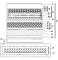
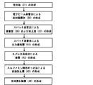
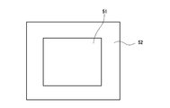
- FIG. 2 is an explanatory exploded view showing a specific configuration of a fluorescent light emitting member and a heat dissipation board in the fluorescent light source device of FIG. 1. It is a flowchart which shows the formation process of the fluorescence light emission member in the fluorescence light source device of FIG. It is explanatory drawing which shows the outline of an example of a structure of the conventional fluorescence light source device. It is a top view for description which shows the fluorescent plate and heat dissipation board in the fluorescence light source device of FIG.
- FIG. 1 is an explanatory diagram showing an outline of an example of the configuration of the fluorescent light source device according to the present invention
- FIG. 2 is an explanatory disassembly showing specific configurations of the fluorescent light emitting member and the heat dissipation substrate in the fluorescent light source device of FIG. FIG.
- the fluorescent light source device 10 includes an excitation light source 11 made of, for example, a semiconductor laser, and a fluorescent light emitting member 20 having a fluorescent plate 21 that emits fluorescence by excitation light from the excitation light source 11. They are spaced apart from each other.
- the fluorescent light source device 10 is provided with a heat dissipation substrate 22 on the back surface side (the lower surface side in FIGS. 1 and 2) of the fluorescent light emitting member 20.
- the fluorescent light emitting member 20 is disposed in a posture inclined with respect to the optical axis of the excitation light source 11 so as to face the excitation light source 11.
- the surface of the flat fluorescent plate 21 (the upper surface in FIGS. 1 and 2) is an excitation light incident surface and a fluorescence emission surface.
- the fluorescent light emitting member 20 has a surface of the flat heat dissipation substrate 22 (upper surface in FIGS. 1 and 2) and a back surface of the fluorescent plate 21 (lower surface in FIGS. 1 and 2) opposed to the surface of the heat dissipation substrate 22. It is arranged and joined in a state.
- a flat joint member layer 26 is formed between the heat dissipation substrate 22 and the fluorescent light emitting member 20. That is, the fluorescent light emitting member 20 and the heat dissipation substrate 22 are joined by the joining member layer 26. Further, the fluorescent light emitting member 20 is disposed so that the surface of the fluorescent plate 21 faces the excitation light source 11.
- the fluorescent plate 21 is a plate-like body containing a phosphor that is excited by excitation light and emits fluorescence.
- the fluorescent plate 21 is a plate-like body made of a phosphor and a metal oxide, specifically, a sintered body of a mixture of a phosphor and a metal oxide, and a portion made of metal oxide particles (
- a plate-like state in which a portion composed of phosphor particles hereinafter also referred to as “phosphor portion” is mixed and a metal oxide portion is exposed on the surface. It is preferable that it is a body.
- the phosphor plate 21 is made of a phosphor and a metal oxide, that is, the metal oxide portion and the phosphor portion are mixed, and the metal oxide portion is exposed on the surface. High adhesion can be obtained between the constituent members of the fluorescent light emitting member 20 stacked in a state (in the example of this figure, a reflective laminate 30 and an adhesive layer 38 to be described later). Further, when the fluorescent plate 21 is made of a phosphor and a metal oxide, since the excitation light and fluorescence guided to the inside of the fluorescent plate 21 are controlled, the light emitting region on the fluorescent emission surface is reduced. It becomes smaller and the light emission luminance is improved.
- the traveling direction of the excitation light that is incident on a certain phosphor portion but is not absorbed is changed at the interface between the phosphor portion and the metal oxide portion.
- a part of the excitation light that has entered the certain phosphor portion but has not been absorbed travels toward the other phosphor portion. Therefore, the optical path length for converting the excitation light into fluorescence becomes longer, and the probability that the excitation light is absorbed by the phosphor portion increases.
- the excitation light incident on the inside of the fluorescent plate 21 can be effectively used and converted into fluorescence with high efficiency.
- the traveling direction of the fluorescence emitted from a certain phosphor portion is changed at the interface between the other phosphor portion and the metal oxide portion, it is suppressed that the fluorescence is confined inside the phosphor plate 21. .
- the fluorescence generated inside the fluorescent plate 21 can be effectively used and emitted to the outside with high efficiency.
- the phosphor plate 21 In the fluorescent plate 21, a polycrystalline phosphor is used as the phosphor. Since the phosphor constituting the phosphor plate 21 is a polycrystalline phosphor, the phosphor plate 21 has high thermal conductivity. For this reason, in the fluorescent plate 21, the heat generated by the irradiation of the excitation light is efficiently exhausted, so that the fluorescent plate 21 is suppressed from becoming a high temperature. As a result, in the fluorescent plate 21, it is possible to suppress a reduction in the amount of fluorescent light caused by temperature quenching occurring in the phosphor.
- the polycrystalline phosphor constituting the fluorescent plate 21 can be obtained, for example, as follows.
- raw materials such as a base material, an activator, a metal oxide, and a firing aid are pulverized by a ball mill or the like to obtain submicron raw material fine particles.
- a molded body is formed and sintered by, for example, a slip casting method.
- a polycrystalline phosphor having a porosity of 0.5% or less, for example, is obtained by subjecting the obtained sintered body to hot isostatic pressing.
- the phosphor constituting the fluorescent plate 21 is preferably made of an inorganic phosphor, specifically, a complex oxide doped with rare earth elements as luminescent ions (activator).
- the phosphor content is, for example, 20 to 80% by mass.
- the particle diameter (average particle diameter) of the phosphor particles is, for example, 1 to 10 ⁇ m.
- aluminum oxide (Al 2 O 3 ) or the like is used as the metal oxide from the viewpoint of exhaust heat (thermal conductivity) and adhesion to the phosphor.
- the fluorescent plate 21 having such a structure is manufactured by, for example, mixing phosphor particles having an appropriate particle diameter and aluminum oxide (Al 2 O 3 ) particles, pressing the mixture, and firing the mixture. can do.
- Specific examples of the material of the fluorescent plate 21 include Al 2 O 3 / YAG: Ce, Al 2 O 3 / YAG: Pr, Al 2 O 3 / YAG: Sm, and Al 2 O 3 / LuAG: Ce. .
- the doping amount of the rare earth element (activator) is about 0.5 mol%.
- the thickness of the fluorescent plate 21 is preferably 0.05 to 2.0 mm from the viewpoint of conversion efficiency of excitation light to fluorescence (quantum yield) and exhaust heat.
- the fluorescent plate 21 may contain at least a light scatterer that diffuses excitation light and may have a light diffusion function of diffusing excitation light.
- the fluorescent plate 21 has a light diffusion function of diffusing excitation light and fluorescence. Since the fluorescent plate 21 has a light diffusion function, the traveling direction of the excitation light is changed by the light scatterer inside the fluorescent plate 21. Therefore, the optical path length for converting the excitation light into fluorescence becomes longer, and the probability that the excitation light is absorbed by the phosphor portion increases. As a result, the excitation light incident on the inside of the fluorescent plate 21 can be effectively used and converted into fluorescence with high efficiency.
- the fluorescent plate 21 has a function of diffusing fluorescence
- the fluorescent traveling direction is changed by the light scatterer inside the fluorescent plate 21, so that the fluorescent light is confined inside the fluorescent plate 21. Is suppressed.
- the fluorescence generated inside the fluorescent plate 21 can be effectively used and emitted to the outside with high efficiency.
- the thickness of the fluorescent plate 21 can be reduced without causing the adverse effect of reducing the conversion efficiency (quantum yield) of excitation light into fluorescence. Can do.
- the fluorescent plate 21 has a very high heat exhaust property, and it is possible to sufficiently suppress or prevent the fluorescence from being emitted from the outer peripheral surface of the fluorescent plate 21 to the outside. Can do.
- the light scatterer contained in the fluorescent plate 21 is composed of aluminum oxide (Al 2 O 3 ) constituting the metal oxide portion of the fluorescent plate 21 or fine particles having a refractive index different from that of the fluorescent material or a grain boundary precipitation phase.
- Al 2 O 3 aluminum oxide
- fine particles constituting the light scatterer include those made of inorganic compounds such as yttria, silicon nitride, aluminum nitride, and strontium fluoride.
- solder containing solder As the joining member constituting the joining member layer 26, it is preferable to use tin-containing solder from the viewpoint of exhaust heat and low stress.
- solder containing tin used as the bonding member include, for example, a gold-tin alloy (AuSn, tin (Sn) content 20 mass%, thermal conductivity 250 W / mk) and a tin-silver-copper alloy (Sn).
- AuSn, tin (Sn) content 20 mass%, thermal conductivity 250 W / mk
- tin-silver-copper alloy Sn
- -3Ag-0.5Cu silver (Ag) content 3 mass%, copper (Cu) content 0.5 mass%, tin (Sn) content 96.5 mass%), thermal conductivity 55 W / mk).
- gold-tin alloys are preferred because of their high thermal conductivity and low tin content.
- the thermal conductivity is high, so that the excitation power of the excitation light is higher than when a tin-silver-copper alloy is used as the joining member. Even if the same, the temperature of the fluorescent screen 21 can be lowered by about 20 degrees. Moreover, since there is little content rate of tin, the fall of the reflectance of the reflection layer 31 can be suppressed. Moreover, the thickness of the joining member layer 26 is, for example, 30 ⁇ m.
- a method of joining the fluorescent light emitting member 20 and the heat radiating substrate 22 by the joining member for example, a reflow furnace is used, and a flux-free solder sheet (joining member) is used between the fluorescent light emitting member 20 and the heat radiating substrate 22.
- a reflow method in which heating is performed in an atmosphere of formic acid gas or hydrogen gas is used.
- the heat radiating substrate 22 exhausts heat generated in the fluorescent light emitting member 20 (specifically, the fluorescent plate 21).
- the heat dissipation substrate 22 is preferably made of a material having high thermal conductivity and a small difference in thermal expansion coefficient from the fluorescent plate 21. Specifically, the thermal expansion coefficient of the constituent material of the heat dissipation substrate 22 is equal to or greater than the thermal expansion coefficient of the constituent material of the fluorescent screen 21, and the difference in thermal expansion coefficient is 9 ⁇ 10 ⁇ 6 [1 / K] or less. Is preferred.
- the operating temperature of the fluorescent plate 21 is set to 150 ° C. or lower.
- the bonding temperature by the bonding member specifically, the solder containing tin
- the bonding member (specifically, the solder containing tin) between the fluorescent light emitting member 20 and the heat dissipation substrate 22 becomes about 100 ° C. Therefore, during the operation of the fluorescent light source device 10, a compressive stress is generated in the fluorescent plate 21, so that no peeling due to thermal expansion occurs between the fluorescent plate 21 and the heat dissipation substrate 22.
- the constituent material of the heat dissipation substrate 22 metals such as copper (Cu) and an alloy of molybdenum and copper (Mo—Cu) are used.
- the thermal expansion coefficient of copper used as a constituent material of the heat dissipation substrate 22 is 16.5 ⁇ 10 ⁇ 6 [1 / K], and an alloy of molybdenum and copper (copper (Cu) content ratio 30 mass%) ) Is 8.6 ⁇ 10 ⁇ 6 [1 / K].
- the thermal expansion coefficient of YAG used as the constituent material of the fluorescent screen 21 is 8.6 ⁇ 10 ⁇ 6 [1 / K].
- the heat dissipation substrate 22 is made of copper.
- the thickness of the heat dissipation substrate 22 may be determined as appropriate in consideration of heat dissipation characteristics, and is, for example, 0.5 to 5.0 mm. Further, as shown in FIGS. 1 and 2, the area of the surface of the heat dissipation substrate 22 is preferably larger than the area of the back surface of the fluorescent plate 21 from the viewpoint of heat exhaustion. Further, the heat dissipation board 22 may have a function of a heat dissipation fin. In the example of this figure, the thickness of the heat dissipation substrate 22 is 2 mm.
- the heat dissipation substrate 22 has a protective film layer 23 and a solder wet film layer 24 on the surface of the heat dissipation substrate 22 as shown in FIG. It is preferable that metal films laminated in order are formed.
- the protective film layer 23 is made of, for example, a nickel (Ni) film formed by a watt bath plating method
- the solder wet film layer 24 is made of, for example, gold (Au) formed by a watt bath plating method. It consists of a film.
- the heat radiating substrate 22 is formed by covering the entire outer surface (front surface, back surface and peripheral side surface) with a metal film composed of the protective film layer 23 and the solder wetting film layer 24.
- the thickness of each layer constituting the metal film is 2.5 ⁇ m for the protective film layer 23 and 0.03 ⁇ m for the solder wetting film layer 24.
- the reflective layer 31 is provided. That is, the reflective layer 31 is disposed opposite to the back surface of the fluorescent plate 21.
- the fluorescent plate 21 has a high reflection function on the back surface by providing the reflection layer 31 made of silver or silver alloy having high reflection characteristics on the back surface side.
- an increased reflection portion 32 made of a metal oxide multilayer film is provided in close contact with the back surface of the fluorescent plate 21.
- the back surface of the fluorescent plate 21 is provided with the increased reflection portion 32 and the reflection layer 31 in this order.
- the metal oxide multilayer film constituting the increased reflection portion 32 has a silicon dioxide (SiO 2 ) layer 32A and a titanium oxide (TiO 2 ) layer 32B.
- the thickness of the metal oxide multilayer film constituting the increased reflection portion 32 is 350 nm.
- the reflective laminate 30 including the silicon dioxide layer 32A and the titanium oxide layer 32B constituting the metal oxide multilayer film is produced by an electron beam evaporation method.
- a laminated film (reflective laminated body 30) is formed on the back surface of the fluorescent plate 21 on which a resist patterned by exposure is disposed by electron beam evaporation. After that, the resist is removed by lift-off.
- the entire surface (upper surface in FIG. 2) of the increased reflection portion 32 is in contact with the central portion of the back surface of the fluorescent plate 21.
- the reflective layer 31 has a thickness of, for example, 110 to 350 nm. Moreover, it is preferable that the area of the surface (upper surface in FIG. 1 and FIG. 2) of the reflection layer 31 is below the area of the back surface of the fluorescent plate 21 from a viewpoint of effective utilization of excitation light and fluorescence. In the example of this figure, the surface of the reflective layer 31 has a size slightly smaller than the size of the back surface of the fluorescent plate 21, and the entire surface faces the central portion of the back surface of the fluorescent plate 21.
- an adhesive improvement layer 35A is provided on the surface of the reflective layer 31 so as to cover the entire surface in a state of being in close contact with the surface.
- an adhesive improvement layer 35B is provided on the back surface (lower surface in FIG. 2) of the reflective layer 31 so as to cover the entire surface in a state of being in close contact with the back surface.
- the reflective layered body 30 is configured by the reflective layer 31, the adhesion improving layers 35 ⁇ / b> A and 35 ⁇ / b> B, and the increased reflection portion 32.
- the adhesion improving layers 35A and 35B are made of aluminum oxide (Al 2 O 3 ).
- the adhesive improvement layers 35A and 35B have a thickness of 1 ⁇ m or less.
- the thickness of the adhesive improvement layers 35A and 35B exceeds 1 ⁇ m, the adhesive improvement layers 35A and 35B have low thermal conductivity, and the temperature of the fluorescent plate 21 during operation of the fluorescent light source device 10 increases. For this reason, a sufficient amount of fluorescent light cannot be obtained due to the occurrence of temperature quenching in the phosphor.
- the thickness of the adhesion improving layer 35A is 50 nm
- the thickness of the adhesion improving layer 35B is 50 nm.
- the reflective laminate 30 is provided with a sealing layer 37 so as to cover the back surface and the peripheral side surface of the reflective layer 31.
- the sealing layer 37 is bonded to the reflective laminate 30 and the fluorescent plate 21 between the reflective laminate 30 and the sealing layer 37 and between the periphery of the back surface of the fluorescent plate 21 and the sealing layer 37.
- the adhesive layer 38 is provided. That is, the adhesive layer 38 is provided in close contact with the back surface and the peripheral side surface of the reflective laminate 30, the peripheral edge of the back surface of the fluorescent plate 21, and the sealing layer 37. In this way, the sealing layer 37 is provided in close contact with the reflective laminate 30 via the adhesive layer 38 on the back surface of the fluorescent plate 21, and the sealing layer 37, the adhesive layer 38, and the fluorescent plate 21 A sealing structure of the reflective laminate 30 is formed.
- the sealing structure of the reflective laminate 30 Since the sealing structure of the reflective laminate 30 is formed, peeling of the constituent layers in the reflective laminate 30 is prevented, and the reflective laminate 30 is exposed to the operating environment atmosphere during the operation of the fluorescent light source device 10. Therefore, the fluorescent light emitting member 20 has excellent weather resistance and moisture resistance. As a result, peeling of the reflective layer 31 from the fluorescent plate 21 and surface deterioration due to oxidation and sulfuration of the reflective layer 31 can be prevented. Further, according to the formation of the sealing structure of the reflective laminate 30, the reflective laminate 30 is formed in the process of forming the fluorescent light emitting member 20 (specifically, the sealing structure of the reflective laminate 30 is formed).
- the reflective laminate 30 has an intended reflection function.
- the sealing layer 37 is made of nickel or indium, and is preferably made of nickel from the viewpoint of weather resistance.
- the sealing layer 37 has a thickness of 0.5 ⁇ m or less, for example.
- the sealing layer 37 is formed by a sputter deposition method or the like. In the example of this figure, the sealing layer 37 is made of nickel, and the thickness of the sealing layer 37 is 110 nm.
- the adhesive layer 38 is made of chromium, a chromium alloy, or titanium.
- the sealing layer 37 is made of nickel, it is made of chromium from the viewpoint of adhesion to the sealing layer 37. It is preferable that The adhesive layer 38 has a thickness of 50 nm, for example, between the reflective laminate 30 and the sealing layer 37 and between the fluorescent plate 21 and the sealing layer 37. Further, the adhesive layer 38 is formed by a sputter deposition method or the like. In the example of this figure, the adhesive layer 38 is made of chromium.
- the region where the adhesive layer 38 is in close contact with the back surface of the fluorescent plate 21, that is, the peripheral edge of the back surface of the fluorescent plate 21, is provided with the adhesive layer 38 made of metal in close contact, thereby having a reflective function. That is, the back surface of the fluorescent plate 21 has a high reflection function at the center and a reflection function at the periphery. This reduces the absorption of fluorescence at the periphery of the back surface of the fluorescent plate 21. Therefore, in the fluorescent light emitting member 20, the fluorescence generated on the fluorescent plate 21 can be taken out efficiently.
- a diffusion prevention layer 45 is provided on the heat dissipation substrate 22 via a bonding member layer 26. That is, in the fluorescent light emitting member 20, the diffusion preventing layer 45 is provided on the back surface side of the sealing layer 37, specifically, between the sealing layer 37 and the bonding member layer 26.
- a metal (specifically, for example, tin) constituting the bonding member layer 26 is formed on the surface of the diffusion preventing layer 45 (see FIG. 1 and the upper surface of FIG. 2) can be prevented from diffusing into the constituent members of the fluorescent light emitting member 20 laminated on the upper surface. Further, in the manufacturing process of the fluorescent light source device 10, the metal constituting the joining member layer 26 is prevented from diffusing into the constituent members of the fluorescent light emitting member 20 in the joining process of the fluorescent light emitting member 20 and the heat dissipation substrate 22. it can.
- the diffusion prevention layer 45 is formed by nickel plating. Since the diffusion prevention layer 45 is formed by a plating method, the diffusion prevention layer 45 becomes denser than that formed by a vapor deposition method, and thus an excellent diffusion prevention function can be obtained. . Further, since the diffusion preventing layer 45 is made of nickel, the diffusion preventing layer 45 is a plating layer formed using a nickel sulfamate plating tank, that is, formed by a plating method using a sulfamic acid bath. Can do. Then, by forming the diffusion prevention layer 45 by a plating method using a sulfamic acid bath, the stress applied to the reflection layer 31 from the diffusion prevention layer 45 can be reduced, thereby preventing the reflection layer 31 from peeling off. can do.
- the diffusion preventing layer 45 made of nickel is formed by a plating method using a sulfamic acid bath
- the stress applied to the reflective layer 31 is 1 to 7 kg / mm 2 , but formed by a plating method using a watt bath.
- the stress applied to the reflective layer 31 is 11 to 13 kg / mm 2 . Therefore, when the diffusion prevention layer 45 is formed by a plating method using a watt bath, peeling is generated at the interface of the reflective layer 31 because the stress applied to the reflective layer 31 is high. Therefore, the diffusion preventing layer 45 is preferably formed by a plating method using a sulfamic acid bath as compared with a plating method using a Watt bath.
- the diffusion prevention layer 45 is preferably formed by a plating method using a highly soluble plating bath from the viewpoint of reducing the stress applied to the reflection layer 31 from the diffusion prevention layer 45 and preventing the reflection layer 31 from peeling off. It is particularly preferable to form by the above-described plating method using a sulfamic acid bath.
- the adhesive layer 38, the sealing layer 37, and the stress relaxation layer 41 described later are formed by a dry method, diffusion is performed.
- the prevention layer 45 by a plating method using a sulfamic acid bath, the fluorescent light source device 10 can obtain high luminous efficiency over a long period of time.
- the fluorescent light source device 10 has a high reflectivity of the reflective layer 31 and the operating temperature of the fluorescent light emitting member 20 (fluorescent plate 21) is 100 ° C. or higher and 250 ° C. or lower. It is assumed that the reflectance of the reflective layer 31 does not decrease.
- the diffusion preventing layer 45 preferably has a thickness of 1 ⁇ m or more and 3 ⁇ m or less. Since the diffusion preventing layer 45 has a thickness in the above range, the operating temperature of the fluorescent light emitting member 20 (fluorescent plate 21) is 200 to 250 ° C. (the junction temperature is 150) when the fluorescent light source device 10 is operating. Even when the temperature reaches ⁇ 200 ° C., the metal constituting the bonding member layer 26 can be prevented from diffusing into the constituent members of the fluorescent light emitting member 20 laminated on the surface of the diffusion preventing layer 45. Moreover, it can prevent that peeling arises between the fluorescent plate 21 and the contact bonding layer 38, and it peels from the fluorescent plate 21 resulting from it.
- the thickness of the diffusion preventing layer 45 when the thickness of the diffusion preventing layer 45 is excessive, peeling may occur between the fluorescent screen 21 and the adhesive layer 38. Further, if the thickness of the diffusion preventing layer 45 is too small, there is a possibility that a sufficient diffusion preventing function cannot be obtained for the diffusion preventing layer 45.
- the reason why a sufficient diffusion preventing function can be obtained when the thickness of the diffusion preventing layer 45 is not less than 1 ⁇ m and not more than 3 ⁇ m will be described.
- sulfamic acid is formed on the back surface of the gold layer 43 (described later) laminated on the back surface of the fluorescent plate 21 via the reflective laminate 30 or the like.
- a diffusion preventing layer 45 made of a nickel plating layer having a thickness of 2 ⁇ m is formed by plating using a bath, and then a solder wetting film layer 46 made of gold and having a thickness of 0.5 ⁇ m is formed.
- the adhesive layer 38, the sealing layer 37, the stress relaxation layer 41, and the gold layer 43 are laminated on the back surface of the fluorescent plate 21, the diffusion prevention layer 45 and the solder wet film layer 46 are formed.
- the fluorescent light emitting member 20 is manufactured.
- a joining member is sandwiched between the obtained fluorescent light emitting member 20 and the heat dissipation substrate 22, and joining is performed by a reflow furnace.
- an intermetallic compound specifically, Sn—Ag—Cu
- a metal specifically, for example, tin
- the surface side of the diffusion preventing layer 45 (specifically, the surface layer portion having a thickness of 1 ⁇ m) remains nickel, and the surface side of the diffusion preventing layer 45 constitutes a bonding member when the fluorescent light source device 10 is operated. Demonstrate metal diffusion prevention function. Therefore, even when the fluorescent light emitting member 20 is operated at a high temperature of 200 to 250 ° C., the diffusion preventing layer 45 prevents diffusion of the metal constituting the bonding member layer 26, and thus the reflective layer 31 has a high reflectance. Can be maintained.
- Table 1 below shows the relationship between the thickness of the diffusion prevention layer 45 formed by nickel plating and the maintenance factor of the reflectance in the reflective layer 31.
- “reflectance maintenance ratio” is the reflection layer 31 after 5000 hours when the temperature (junction temperature) during operation of the fluorescent light emitting member 20 is 150 ° C., 175 ° C., and 200 ° C. It is the maintenance factor of the reflectance, the “thickness of the diffusion preventing layer” is the thickness of the nickel plating layer formed by the plating method using a sulfamic acid bath, and the “thickness of the surface layer portion” is the fluorescent light emitting member 20 and the heat dissipation substrate 22. Is the thickness of the portion other than the back surface where the intermetallic compound of the nickel plating layer is formed, that is, the thickness of the surface layer portion as it is.
- a stress relaxation layer 41 is provided between the diffusion prevention layer 45 and the sealing layer 37 as shown in FIG. 2.
- the stress relaxation layer 41 internal stress generated in the sealing layer 37 can be relaxed. Therefore, it is possible to prevent the separation between the fluorescent plate 21 and the sealing layer 37 and the separation of the reflective layer 31 from the fluorescent plate 21 due to the separation.
- a gold layer 43 having a thickness of 500 nm formed by a sputter deposition method is provided on the back surface of the diffusion prevention layer 45 (the lower surface in FIG. 2).
- the stress relaxation layer 41 is made of a material having a thermal expansion coefficient that approximates the thermal expansion coefficient of the fluorescent screen 21, and may be made of a single layer film made of one kind of material, or two or more kinds of materials. It may be composed of a multilayer film having a constituent layer composed of In the example of this figure, the stress relaxation layer 41 is composed of a multilayer film having titanium (Ti) layers 41A and 41B and platinum (Pt) layers 42A and 42B, and these layers are each formed by sputtering deposition. It is a thing. In this multilayer film, the thickness of the titanium layer 41A in contact with the sealing layer 37 is 50 nm, and the thickness of the platinum layer 42A in contact with the titanium layer 41A is 150 nm.
- the titanium layer 41B in contact with the platinum layer 42A has a thickness of 100 nm, and the platinum layer 42B in contact with the titanium layer 41B has a thickness of 200 nm.
- the thermal expansion coefficient of titanium (8.5 ⁇ 10 ⁇ 6 [1 / K]) and the thermal expansion coefficient of platinum (8.9 ⁇ 10 ⁇ 6 [1 / K]) Since it approximates the thermal expansion coefficient (8.6 ⁇ 10 ⁇ 6 [1 / K]) of YAG used as the constituent material of the fluorescent plate 21, the internal stress generated in the sealing layer 37 can be relaxed.
- the platinum layers 42 ⁇ / b> A and 42 ⁇ / b> B exhibit a function of preventing diffusion of a metal (specifically, for example, tin) constituting the bonding member layer 26. That is, the platinum layers 42 ⁇ / b> A and 42 ⁇ / b> B function as a diffusion preventing layer together with the diffusion preventing layer 45.
- a metal specifically, for example, tin
- the excitation light emitted from the excitation light source 11 is irradiated on the surface (excitation light incident surface) of the fluorescent plate 21 and is incident on the fluorescent plate 21.
- the fluorescent substance which comprises the said fluorescent plate 21 is excited.
- fluorescence is emitted from the phosphor in the fluorescent plate 21.
- the fluorescence is emitted from the surface (fluorescence emission surface) of the fluorescent plate 21 to the outside together with the excitation light reflected by the reflective layer 31 on the back surface of the fluorescent plate 21 without being absorbed by the phosphor, and is emitted to the outside of the fluorescent light source device 10.
- the diffusion preventing layer 45 is formed on the heat dissipation substrate 22 via the bonding member layer 26 on the back surface side of the sealing layer 37. Therefore, it is possible to prevent the reflectance of the reflective layer 31 from decreasing with time due to the constituent material (joining member) of the bonding member layer 26 diffusing into the reflective layer 31 during the operation of the fluorescent light source device 10. it can. Therefore, even when a metal containing tin is used as the constituent material of the bonding member layer 26, tin having a low reflectance is not diffused in the reflective layer 31.
- the constituent material of the joining member layer 26 diffuses into the reflective layer 31, and thus the reflective layer 31. Can be prevented from decreasing. Therefore, in the fluorescent light source device 10, the reflective laminate 30 has an intended reflection function. Further, in the fluorescent light source device 10, the sealing structure of the reflective laminate 30 is formed by the fluorescent plate 21, the sealing layer 37, and the adhesive layer 38. Therefore, the reflective layer 31 is in close contact with the fluorescent plate 21 via the adhesion improving layer 35 ⁇ / b> A and the increased reflection portion 32 on the back side of the fluorescent plate 21.
- the reflective laminate 30 is not exposed to an environmental atmosphere such as the atmosphere and the manufacturing environment atmosphere after the sealing structure of the reflective laminate 30 in the manufacturing process of the fluorescent light source device 10 is formed. It is possible to prevent the reflectance of the reflective layer 31 from being lowered due to the surface degradation of the layer 31 due to oxidation, sulfurization, or the like. Therefore, according to the fluorescent light source device 10, high reliability can be obtained without causing a reduction in reflectance over a long period of time.
- the fluorescent light source device 10 when the thickness of the diffusion prevention layer 45 is 1 ⁇ m or more and 3 ⁇ m or less, the fluorescent light source device 10 is driven under a driving condition in which the temperature of the back surface of the fluorescent plate 21 is high.
- the metal constituting the bonding member layer 26 can be prevented from diffusing into the constituent members of the fluorescent light emitting member 20 laminated on the surface of the diffusion preventing layer 45.
- it can prevent that peeling arises between the fluorescent plate 21 and the contact bonding layer 38, and it peels from the fluorescent plate 21 resulting from it.
- the diffusion prevention layer 45 is a plating layer formed using a nickel sulfamate plating tank, the stress applied to the reflection layer 31 from the diffusion prevention layer 45 can be reduced. Therefore, peeling of the reflective layer 31 can be prevented.
- the internal stress generated in the sealing layer 37 is relieved by providing the fluorescent light emitting member 20 with the stress relieving layer 41. Therefore, it is possible to prevent the separation between the fluorescent plate 21 and the sealing layer 37 and the separation of the reflective layer 31 from the fluorescent plate 21 due to the separation.
- the fluorescent plate may have a periodic structure in which a plurality of convex portions are periodically arranged on the surface of the fluorescent plate.
- the periodic structure on the surface of the fluorescent plate is, for example, a two-dimensional periodic arrangement in which convex portions having a substantially cone shape (specifically, a cone shape or a frustum shape) are densely packed.
- the fluorescent plate has a periodic structure on the surface, the fluorescent plate is composed of a fluorescent member and a periodic structure layer having optical transparency to excitation light and fluorescence from the viewpoint of ease of manufacture. It may be.
- the overall structure of the fluorescent light source device is not limited to that shown in FIG. 1, and various configurations can be employed.
- the light of one excitation light source for example, a semiconductor laser
- a condensing lens is arranged in front of the fluorescent light emitting member.
- the form which irradiates light light to a fluorescence light-emitting member may be sufficient.
- the excitation light is not limited to light from a semiconductor laser, but may be one that collects light from an LED as long as it can excite the phosphor in the fluorescent plate, and further contains mercury, xenon, or the like. It may be light from a lamp that has been made.
- the wavelength of the excitation light is the main emission wavelength region.
- the present invention is not limited to this.
Landscapes
- Engineering & Computer Science (AREA)
- Chemical & Material Sciences (AREA)
- General Engineering & Computer Science (AREA)
- Physics & Mathematics (AREA)
- Materials Engineering (AREA)
- Mechanical Engineering (AREA)
- Metallurgy (AREA)
- Organic Chemistry (AREA)
- Chemical Kinetics & Catalysis (AREA)
- Microelectronics & Electronic Packaging (AREA)
- Optics & Photonics (AREA)
- Health & Medical Sciences (AREA)
- Toxicology (AREA)
- Spectroscopy & Molecular Physics (AREA)
- Non-Portable Lighting Devices Or Systems Thereof (AREA)
- Led Device Packages (AREA)
Abstract
Description
このような蛍光光源装置の或る種のものは、図4および図5に示すように、半導体レーザなどの励起光源11からの励起光によって蛍光を放射する蛍光体を含有し、表面(図4)における上面)が励起光入射面とされた蛍光板51と、当該蛍光板51の裏面(図4における下面)側に設けられた放熱基板52とを備えている(例えば、特許文献1参照)。この蛍光光源装置において、蛍光板51は、反射層が設けられることなどによって裏面が反射機能を有するものとされている。この反射層は、高い光反射特性を有する金属からなるものであることが好ましく、反射層を構成する金属としては、アルミニウム(Al)、銀(Ag)などが用いられる。そして、蛍光板51に設けられた反射層と放熱基板52との間には、例えば半田などの金属からなる接合部材層53が介在しており、当該接合部材層53によって蛍光板51が放熱基板52上に接合されている。
このような表面劣化および接合部材に含まれる金属の拡散に起因する反射層の反射率の低下の問題は、反射層に対して、耐候性用の保護層および接合部材に含まれる物質の拡散防止層の両方が設けられていない場合、保護層および拡散防止層のいずれか一方のみが設けられている場合、および両方が設けられていたとしても保護層の密着性が十分でない場合のいずれの場合にも生じる。また、この反射層の反射率の低下の問題は、反射層として銀(Ag)または銀を主体とする銀合金を用い、接合部材として、例えば半田などのスズ(Sn)を含有する金属を用いた場合に顕著である。
前記反射層の裏面、および、周側面を覆う封止層が、接着層を介して、前記蛍光板の裏面の周縁に密着して設けられており、
前記放熱基板上に、接合部材層を介して、ニッケルめっきにより形成された拡散防止層が設けられていることを特徴とする。
また、蛍光板の裏面側においては、反射層の裏面および周側面を覆う封止層が、接着層を介して当該蛍光板の裏面の周縁に密着して設けられることにより、反射層の封止構造が形成されている。そのため、反射層が大気などの環境雰囲気にさらされることがないことから、酸化および硫化などによる表面劣化に起因する当該反射層の反射率の低下を防止することができる。
従って、本発明の蛍光光源装置によれば、長期間にわたって反射率の低下が生じることのない高い信頼性が得られる。
図1は、本発明の蛍光光源装置の構成の一例の概略を示す説明図であり、図2は、図1の蛍光光源装置における蛍光発光部材および放熱基板の具体的な構成を示す説明用分解図である。
この蛍光光源装置10は、図1に示すように、例えば半導体レーザよりなる励起光源11と、励起光源11からの励起光によって蛍光を出射する蛍光板21を有する蛍光発光部材20とを備え、これらが互いに離間して配設されたものである。また、蛍光光源装置10には、蛍光発光部材20の裏面側(図1および図2における下面側)に、放熱基板22が設けられている。
この図の例において、蛍光発光部材20は、励起光源11に対向するよう、当該励起光源11の光軸に対して傾斜した姿勢で配置されている。
この蛍光発光部材20は、平板状の放熱基板22の表面(図1および図2における上面)に、蛍光板21の裏面(図1および図2における下面)が、当該放熱基板22の表面に対向した状態で配置されて接合されたものである。そして、放熱基板22と蛍光発光部材20との間には、平板状の接合部材層26が形成されている。すなわち、蛍光発光部材20と放熱基板22とは、接合部材層26によって接合されている。
また、蛍光発光部材20は、蛍光板21の表面が、励起光源11に対向するように配置されている。
また、蛍光板21は、蛍光体と金属酸化物とからなる板状体、具体的には、蛍光体と金属酸化物との混合物の焼結体であって、金属酸化物の粒子からなる部分(以下、「金属酸化物部分」ともいう。)と蛍光体の粒子からなる部分(以下、「蛍光体部分」ともいう。)とが混在し、表面に金属酸化物部分が露出した状態の板状体であることが好ましい。
また、蛍光板21が蛍光体と金属酸化物とからなるものであることによれば、蛍光板21の内部に入射した励起光および蛍光の導光が制御されることから、蛍光出射面における発光領域が小さくなり発光輝度が向上する。また、蛍光板21の内部において、或る蛍光体部分に入射したものの吸収されることのなかった励起光の進行方向が当該蛍光体部分と金属酸化物部分との界面において変更される。そして、その或る蛍光体部分に入射したものの吸収されることのなかった励起光の一部は、他の蛍光体部分に向かって進行する。そのため、励起光を蛍光に変換するための光路長が長くなり、励起光が蛍光体部分に吸収される確率が高くなる。その結果、蛍光板21の内部に入射した励起光を有効に利用して、高い効率で蛍光に変換することができる。また、或る蛍光体部分から放射された蛍光の進行方向が他の蛍光体部分と金属酸化物部分との界面において変更されることから、蛍光が蛍光板21の内部に閉じ込められることが抑制される。その結果、蛍光発光部材20においては、蛍光板21の内部において生じた蛍光を有効に利用して、高い効率で外部に出射することができる。
蛍光板21を構成する蛍光体が多結晶の蛍光体であることにより、蛍光板21が高い熱伝導性を有するものとなる。そのため、蛍光板21においては励起光の照射によって発生した熱が効率よく排熱されることから、蛍光板21が高温となることが抑制される。その結果、蛍光板21においては、蛍光体において温度消光が生じることに起因する蛍光光量の低減を抑制することができる。
ここに、蛍光板21を構成する多結晶の蛍光体は、例えば以下のようにして得ることができる。先ず、母材、賦活材、金属酸化物および焼成助剤などの原材料をボールミルなどによって粉砕処理することによって、サブミクロン以下の原材料微粒子を得る。次いで、この原材料微粒子を用い、例えばスリップキャスト法によって成形体を形成して焼結する。その後、得られた焼結体に対して熱間等方圧加圧加工を施すことによって、気孔率が例えば0.5%以下の多結晶の蛍光体が得られる。
また、蛍光体の粒子の粒径(平均粒径)は、例えば1~10μmである。
蛍光板21の材質の具体例としては、Al2 O3 /YAG:Ce、Al2 O3 /YAG:Pr、Al2 O3 /YAG:Sm、およびAl2 O3 /LuAG:Ceなどが挙げられる。このような蛍光板21の蛍光体において、希土類元素(賦活材)のドープ量は、0.5mol%程度である。
蛍光板21が光拡散機能を有するものであることにより、蛍光板21の内部において、励起光の進行方向が光散乱体によって変更される。そのため、励起光を蛍光に変換するための光路長が長くなり、励起光が蛍光体部分に吸収される確率が高くなる。その結果、蛍光板21の内部に入射した励起光を有効に利用して、高い効率で蛍光に変換することができる。
また、蛍光板21が蛍光を拡散する機能を有するものである場合には、蛍光板21の内部において、蛍光の進行方向が光散乱体によって変更されることから、蛍光が蛍光板21の内部に閉じ込められることが抑制される。その結果、蛍光発光部材20においては、蛍光板21の内部において生じた蛍光を有効に利用して、高い効率で外部に出射することができる。
しかも、蛍光板21が光拡散機能を有するものであることによれば、励起光の蛍光への変換効率(量子収率)が小さくなるという弊害を生じさせることなく、蛍光板21の厚みを小さくすることができる。そして、蛍光板21の厚みを小さくすることによれば、当該蛍光板21が極めて高い排熱性を有するものとなり、また蛍光板21の外周面から蛍光が外部に出射されることを十分に抑制または防止することができる。
接合部材として用いられるスズを含有する半田の具体例としては、例えば金スズ合金(AuSn,スズ(Sn)の含有割合20質量%,熱伝導率250W/mk)およびスズ-銀-銅合金(Sn-3Ag-0.5Cu(銀(Ag)の含有割合3質量%,銅(Cu)の含有割合0.5質量%,スズ(Sn)の含有割合96.5質量%),熱伝導率55W/mk)などが挙げられる。これらのうちでは、熱伝導率が高く、スズの含有量が少ないため、金スズ合金が好ましい。具体的に説明すると、接合部材として金スズ合金を用いた場合には、熱伝導率が高いことから、接合部材としてスズ-銀-銅合金を用いた場合に比して、励起光の励起パワーが同一であっても、蛍光板21の温度を20deg程低くすることができる。また、スズの含有割合が少ないことから、反射層31の反射率の低下を抑制することができる。
また、接合部材層26の厚みは、例えば30μmである。
この図の例において、接合部材による蛍光発光部材20と放熱基板22との接合方法としては、例えばリフロー炉を用い、フラックスフリー半田シート(接合部材)を、蛍光発光部材20と放熱基板22との間に挟み、蟻酸ガスまたは水素ガスの雰囲気中において加熱を行うリフロー方式が用いられている。このように、蟻酸または水素の還元力を利用してフラックスフリー半田シートの表面酸化膜を除去してリフローを行う接合方法によれば、形成される接合部材層26にボイドが生じることがなく、良好な熱伝導性が得られる。
この放熱基板22は、高熱伝導性を有すると共に、蛍光板21との熱膨張係数の差が小さい材料よりなるものであることが好ましい。
具体的には、放熱基板22の構成材料の熱膨張係数は蛍光板21の構成材料の熱膨張係数以上であり、その熱膨張係数の差は9×10⁻⁶〔1/K〕以下であることが好ましい。
放熱基板22の構成材料と蛍光板21の構成材料との熱膨張係数の差が9×10⁻⁶〔1/K〕以下であることによれば、蛍光板21の動作時温度を150℃以下に設定することにより、蛍光光源装置10の製造工程において、蛍光発光部材20と放熱基板22との接合部材(具体的には、スズを含有する半田)による接合温度が100℃程度となる。そのため、蛍光光源装置10の動作時においては、蛍光板21に圧縮応力が発生した状態となることから、蛍光板21と放熱基板22との間に、熱膨張に起因する剥離が生じることがない。
ここに、放熱基板22の構成材料として用いられる銅の熱膨張係数は16.5×10⁻⁶〔1/K〕であり、モリブデンと銅との合金(銅(Cu)の含有割合30質量%)の熱膨張係数は8.6×10-6〔1/K〕である。一方、蛍光板21の構成材料として用いられるYAGの熱膨張係数は8.6×10-6〔1/K〕である。
図の例において、放熱基板22は、銅よりなるものである。
また、放熱基板22の表面の面積は、図1および図2に示されているように、排熱性などの観点から、蛍光板21の裏面の面積よりも大きいことが好ましい。
また、放熱基板22は、放熱フィンの機能を兼ね備えたものであってもよい。
この図の例において、放熱基板22の厚みは2mmである。
この金属膜において、保護膜層23は、例えばワット浴によるめっき法によって形成されたニッケル(Ni)膜よりなり、半田濡れ膜層24は、例えばワット浴によるめっき法によって形成された金(Au)膜よりなる。
この図の例において、放熱基板22は、外表面全面(表面、裏面および周側面)が、保護膜層23および半田濡れ膜層24よりなる金属膜で覆われてなるものである。この金属膜を構成する各層の厚みは、保護膜層23が2.5μm、半田濡れ膜層24が0.03μmである。
この図の例において、反射層31と蛍光板21との間には、金属酸化物多層膜よりなる増反射部32が、蛍光板21の裏面に密着した状態で設けられている。すなわち、蛍光板21の裏面には、増反射部32と反射層31とがこの順に設けられている。この増反射部32を構成する金属酸化物多層膜は、二酸化ケイ素(SiO2 )層32Aと酸化チタン(TiO2 )層32Bとを有するものである。ここに、増反射部32を構成する金属酸化物多層膜の厚みは、350nmである。この金属酸化物多層膜を構成する二酸化ケイ素層32Aおよび酸化チタン層32Bを含む反射積層体30は、電子ビーム蒸着法によって作製される。具体的には、露光によってパターニングしたレジストが配設された蛍光板21の裏面上に、電子ビーム蒸着法によって積層膜(反射積層体30)を成膜する。その後、レジストをリフトオフによって取り除き作製されたものである。また、増反射部32の表面(図2における上面)は、その全面が蛍光板21の裏面の中央部に対向接触している。
また、反射層31の表面(図1および図2における上面)の面積は、励起光および蛍光の有効利用性の観点から、蛍光板21の裏面の面積以下であることが好ましい。
この図の例において、反射層31の表面は、蛍光板21の裏面の寸法よりも僅かに小さな寸法を有しており、その全面が蛍光板21の裏面の中央部に対向している。
反射層31の表裏面の各々に接着性改善層35A,35Bが設けられていることにより、反射層31と、当該接着性改善層35A,35Bを介して反射層31に積層される蛍光発光部材20の構成部材との間に高い密着性が得られる。
この図の例において、接着性改善層35Aの上面(図2における上面)には、増反射部32が密着した状態で配設されている。すなわち、接着性改善層35Aと蛍光板21との間においては、増反射部32が、接着性改善層35Aおよび蛍光板21の各々に密着した状態とされている。そして、反射層31と接着性改善層35A,35Bと増反射部32とによって反射積層体30が構成されている。
接着性改善層35A,35Bの厚みが1μmを超える場合には、接着性改善層35A,35Bが熱伝導性の低いものとなり、蛍光光源装置10の動作時における蛍光板21の温度が高くなる。そのため、蛍光体において温度消光が生じることに起因して十分な蛍光光量を得ることができなくなる。
この図の例において、接着性改善層35Aの厚みは50nmであり、接着性改善層35Bの厚みは50nmである。
また、反射積層体30と封止層37との間、および蛍光板21の裏面の周縁と封止層37との間には、封止層37を、反射積層体30および蛍光板21に接着するための接着層38が設けられている。すなわち、接着層38は、反射積層体30における裏面および周側面と、蛍光板21の裏面の周縁と、封止層37とに密着した状態で設けられている。
このようにして、蛍光板21の裏面において、封止層37が接着層38を介して反射積層体30に密着して設けられており、この封止層37と接着層38と蛍光板21とにより、反射積層体30の封止構造が形成されている。
また、反射積層体30の封止構造が形成されていることによれば、反射積層体30が、蛍光発光部材20の形成過程(具体的には、反射積層体30の封止構造を形成した後における蛍光発光部材20の構成層の形成過程)、および蛍光発光部材20と放熱基板22との接合過程などの蛍光光源装置10の製造工程における製造環境雰囲気にさらされることを防止できる。そのため、蛍光光源装置10において、反射積層体30が所期の反射機能を有するものとなる。
また、封止層37は、その厚みが、例えば0.5μm以下とされる。
この封止層37は、スパッタ蒸着法などによって形成される。
この図の例において、封止層37は、ニッケルからなるものであり、当該封止層37の厚みは110nmである。
この接着層38は、反射積層体30と封止層37との間および蛍光板21と封止層37との間の各々において、例えば50nmの厚みを有するものである。
また、接着層38は、スパッタ蒸着法などによって形成される。
この図の例において、接着層38は、クロムよりなるものである。また、蛍光板21の裏面における接着層38が密着した領域、すなわち蛍光板21の裏面の周縁は、金属よりなる接着層38が密着して設けられることにより、反射機能を有するものとされている。すなわち、蛍光板21の裏面は、中央が高反射機能を有し、周縁が反射機能を有するものとされている。このことによって、蛍光板21の裏面の周縁における蛍光の吸収が少なくなる。そのため、蛍光発光部材20においては、蛍光板21で発生した蛍光を効率よく取り出すことができる。
拡散防止層45がめっき法により形成されたものであることにより、当該拡散防止層45は、蒸着法によって形成された場合に比して緻密なものとなるため、優れた拡散防止機能が得られる。
また、拡散防止層45がニッケルよりなるものであることにより、当該拡散防止層45を、スルファミン酸ニッケルめっき槽を用いて形成されためっき層とする、すなわちスルファミン酸浴によるめっき法で形成することができる。そして、拡散防止層45をスルファミン酸浴によるめっき法で形成することによれば、当該拡散防止層45から反射層31に負荷される応力を小さくすることができ、よって反射層31の剥離を防止することができる。
ここに、ニッケルよりなる拡散防止層45を、スルファミン酸浴によるめっき法で形成した場合において、反射層31に負荷される応力は1~7kg/mm2 であるが、ワット浴によるめっき法で形成した場合に反射層31に負荷される応力は11~13kg/mm2 となる。そのため、ワット浴によるめっき法によって拡散防止層45を形成した場合には、反射層31に負荷される応力が高いことから、反射層31の界面で剥離が発生する。従って、拡散防止層45は、ワット浴によるめっき法に比してスルファミン酸浴によるめっき法によって形成することが好ましい。
蛍光発光部材20の形成過程において、図3のフローチャートに示されているように、反射積層体30、接着層38、封止層37および後述する応力緩和層41を乾式法によって形成した後、拡散防止層45をスルファミン酸浴によるめっき法で形成することによれば、蛍光光源装置10が長期間にわたって高い発光効率が得られるものとなる。具体的には、蛍光光源装置10を、反射層31の反射率が高く、しかも蛍光発光部材20(蛍光板21)の動作時温度が100℃以上であって250℃以下の温度範囲内にある場合において当該反射層31の反射率が低下しないものとすることができる。
拡散防止層45が上記の範囲の厚みを有するものであることにより、蛍光光源装置10の動作時において、蛍光発光部材20(蛍光板21)の動作時温度が200~250℃(接合部温度が150~200℃)となった場合であっても、接合部材層26を構成する金属が拡散防止層45の表面上に積層された蛍光発光部材20の構成部材に拡散されることを防止できる。また、蛍光板21と接着層38との間において剥離が生じ、それに起因して反射層31の蛍光板21からの剥離が生じることを防止できる。
一方、拡散防止層45の厚みが過大である場合には、蛍光板21と接着層38との間において剥離が生じるおそれがある。
また、拡散防止層45の厚みが過小である場合には、当該拡散防止層45に十分な拡散防止機能が得られなくなるおそれがある。
蛍光発光部材20の形成過程においては、図3のフローチャートに示されているように、蛍光板21の裏面に反射積層体30などを介して積層された後述する金層43の裏面に、例えばスルファミン酸浴によるめっき法により厚み2μmのニッケルめっき層よりなる拡散防止層45を形成し、その後、金よりなる厚み0.5μmの半田濡れ膜層46を形成する。このように、蛍光板21の裏面に反射積層体30、接着層38、封止層37、応力緩和層41および金層43を積層した後、拡散防止層45および半田濡れ膜層46を形成することにより、蛍光発光部材20が製造される。そして、得られた蛍光発光部材20と放熱基板22との間に接合部材を挟んでリフロー炉によって接合を行なう。この接合過程を経ることにより、拡散防止層45においては、接合部材を構成する金属(具体的には、例えばスズ)の拡散によって裏面側に金属間化合物(具体的には、Sn-Ag-Cuを主体とした金属間化合物)が形成される。しかし、前記拡散防止層45の表面側(具体的には、厚み1μmの表層部分)はニッケルのままであり、その拡散防止層45の表面側が、蛍光光源装置10の動作時において接合部材を構成する金属の拡散防止機能を発揮する。そのため、蛍光発光部材20の動作時温度が200~250℃となる高温動作時においても、拡散防止層45が接合部材層26を構成する金属の拡散を防止し、よって反射層31が高い反射率を維持することができる。
ここに、ニッケルめっきにより形成された拡散防止層45の厚みと反射層31における反射率の維持率との関係を、下記の表1に示す。表1において、「反射率の維持率」は、蛍光発光部材20の動作時の温度(接合部温度)が150℃、175℃および200℃である場合における、5000時間経過後の反射層31の反射率の維持率であり、「拡散防止層の厚み」は、スルファミン酸浴によるめっき法によって形成したニッケルめっき層の厚みであり、「表層部分の厚み」は、蛍光発光部材20と放熱基板22とを接合した後における、当該ニッケルめっき層の金属間化合物が形成された裏面側以外の部分、すなわちニッケルのままの表層部分の厚みである。

応力緩和層41が設けられていることにより、封止層37において発生する内部応力を緩和することができる。そのため、蛍光板21と封止層37との間において剥離が生じ、それに起因して反射層31の蛍光板21からの剥離が生じることを防止できる。
この図の例において、拡散防止層45の裏面(図2における下面)には、スパッタ蒸着法によって形成された、厚み500nmの金層43が設けられている。
この図の例において、応力緩和層41は、チタン(Ti)層41A,41Bと白金(Pt)層42A,42Bとを有する多層膜よりなり、これらの層が、各々、スパッタ蒸着法によって作製されたものである。この多層膜において、封止層37に接触しているチタン層41Aの厚みは50nmであり、そのチタン層41Aに接触している白金層42Aの厚みは150nmである。また、白金層42Aに接触しているチタン層41Bの厚みは100nmであり、そのチタン層41Bに接触している白金層42Bの厚みは200nmである。このような多層膜によれば、チタンの熱膨張係数(8.5×10⁻⁶〔1/K〕)および白金の熱膨張係数(8.9×10-6〔1/K〕)が、蛍光板21の構成材料として用いられるYAGの熱膨張係数(8.6×10-6〔1/K〕)に近似しているため、封止層37で発生する内部応力の緩和が可能となる。また、白金層42A,42Bは、接合部材層26を構成する金属(具体的には、例えばスズ)の拡散防止機能を発揮する。すなわち、白金層42A,42Bは、拡散防止層45と共に拡散防止層としても機能する。
更に、蛍光光源装置10においては、蛍光板21と封止層37と接着層38とによって反射積層体30の封止構造が形成されている。そのため、反射層31は、蛍光板21の裏面側において、接着性改善層35Aおよび増反射部32を介して蛍光板21に密着した状態とされる。また、反射積層体30が、大気などの環境雰囲気、および蛍光光源装置10の製造工程における反射積層体30の封止構造が形成された後の製造環境雰囲気にさらされることがないことから、反射層31が酸化および硫化などによって表面劣化されることに起因する当該反射層31の反射率の低下を防止できる。
従って、蛍光光源装置10によれば、長期間にわたって反射率の低下が生じることのない高い信頼性が得られる。
例えば、蛍光板は、当該蛍光板の表面に、複数の凸部が周期的に配列されてなる周期構造が形成されたものであってもよい。ここに、蛍光板の表面の周期構造は、例えば略錐形状(具体的には、錐状または錐台状)の凸部が密集した状態で二次元周期的に配列されてなるものである。また、蛍光板が表面に周期構造を有するものである場合には、その蛍光板は、製造容易性の観点から、蛍光部材と、励起光および蛍光に対する光透過性を有する周期構造体層とからなるものであってもよい。
11 励起光源
20 蛍光発光部材
21 蛍光板
22 放熱基板
23 保護膜層
24 半田濡れ膜層
26 接合部材層
30 反射積層体
31 反射層
32 増反射部
32A 二酸化ケイ素層
32B 酸化チタン層
35A,35B 接着性改善層
37 封止層
38 接着層
41 応力緩和層
41A,41B チタン層
42A,42B 白金層
43 金層
45 拡散防止層
46 半田濡れ膜層
51 蛍光板
52 放熱基板
53 接合部材層
Claims (4)
- 励起光により蛍光を発する、表面が励起光入射面とされた蛍光板と、当該蛍光板の裏面側に配置された反射層と、放熱基板とを具備した蛍光光源装置において、
前記反射層の裏面、および、周側面を覆う封止層が、接着層を介して、前記蛍光板の裏面の周縁に密着して設けられており、
前記放熱基板上に、接合部材層を介して、ニッケルめっきにより形成された拡散防止層が設けられていることを特徴とする蛍光光源装置。 - 前記拡散防止層は、厚みが1μm以上3μm以下であることを特徴とする請求項1に記載の蛍光光源装置。
- 前記拡散防止層は、スルファミン酸ニッケルめっき槽を用いて形成されためっき層であることを特徴とする請求項1に記載の蛍光光源装置。
- 前記拡散防止層と前記封止層との間に、応力緩和層が設けられていることを特徴とする請求項1に記載の蛍光光源装置。
Priority Applications (3)
| Application Number | Priority Date | Filing Date | Title |
|---|---|---|---|
| CN201680015706.2A CN107429906B (zh) | 2015-03-31 | 2016-02-23 | 荧光光源装置 |
| KR1020177026413A KR101877193B1 (ko) | 2015-03-31 | 2016-02-23 | 형광 광원 장치 |
| US15/561,565 US9989215B2 (en) | 2015-03-31 | 2016-02-23 | Fluorescence light source apparatus |
Applications Claiming Priority (2)
| Application Number | Priority Date | Filing Date | Title |
|---|---|---|---|
| JP2015-071277 | 2015-03-31 | ||
| JP2015071277A JP6020637B1 (ja) | 2015-03-31 | 2015-03-31 | 蛍光光源装置 |
Publications (1)
| Publication Number | Publication Date |
|---|---|
| WO2016158089A1 true WO2016158089A1 (ja) | 2016-10-06 |
Family
ID=57004954
Family Applications (1)
| Application Number | Title | Priority Date | Filing Date |
|---|---|---|---|
| PCT/JP2016/055163 Ceased WO2016158089A1 (ja) | 2015-03-31 | 2016-02-23 | 蛍光光源装置 |
Country Status (5)
| Country | Link |
|---|---|
| US (1) | US9989215B2 (ja) |
| JP (1) | JP6020637B1 (ja) |
| KR (1) | KR101877193B1 (ja) |
| CN (1) | CN107429906B (ja) |
| WO (1) | WO2016158089A1 (ja) |
Cited By (1)
| Publication number | Priority date | Publication date | Assignee | Title |
|---|---|---|---|---|
| TWI840409B (zh) * | 2018-10-19 | 2024-05-01 | 日商大阪瓦斯股份有限公司 | 熱輻射光源 |
Families Citing this family (10)
| Publication number | Priority date | Publication date | Assignee | Title |
|---|---|---|---|---|
| JP2019532497A (ja) | 2016-08-30 | 2019-11-07 | テラダイオード, インコーポレーテッド | カーボンナノチューブを利用した高出力レーザパッケージング |
| JP2018159742A (ja) * | 2017-03-22 | 2018-10-11 | セイコーエプソン株式会社 | 波長変換素子、光源装置及びプロジェクター |
| JP6981086B2 (ja) * | 2017-08-03 | 2021-12-15 | セイコーエプソン株式会社 | 波長変換素子、光源装置及びプロジェクター |
| JP6977527B2 (ja) * | 2017-12-13 | 2021-12-08 | セイコーエプソン株式会社 | 波長変換素子、波長変換素子の製造方法、光源装置及びプロジェクター |
| JP6888546B2 (ja) * | 2017-12-28 | 2021-06-16 | ウシオ電機株式会社 | 蛍光プレート |
| JP2019164258A (ja) * | 2018-03-20 | 2019-09-26 | セイコーエプソン株式会社 | 波長変換素子、波長変換素子の製造方法、光源装置及びプロジェクター |
| WO2020002074A1 (en) * | 2018-06-26 | 2020-01-02 | Lumileds Holding B.V. | Light converting device with ceramic protection layer |
| JP7312829B2 (ja) * | 2019-07-16 | 2023-07-21 | 日本特殊陶業株式会社 | 半田付け用波長変換部材、波長変換装置、および、光源装置 |
| JP7307616B2 (ja) * | 2019-07-16 | 2023-07-12 | 日本特殊陶業株式会社 | 波長変換部材 |
| US20230235978A1 (en) * | 2021-03-17 | 2023-07-27 | Amulaire Thermal Technology, Inc. | Heat-dissipating substrate with coating structure |
Citations (4)
| Publication number | Priority date | Publication date | Assignee | Title |
|---|---|---|---|---|
| WO2014065051A1 (ja) * | 2012-10-26 | 2014-05-01 | ウシオ電機株式会社 | 蛍光光源装置 |
| JP2014179231A (ja) * | 2013-03-14 | 2014-09-25 | Toshiba Lighting & Technology Corp | 光源装置及び照明装置 |
| JP2014192127A (ja) * | 2013-03-28 | 2014-10-06 | Ushio Inc | 蛍光光源装置 |
| JP2014194895A (ja) * | 2013-03-29 | 2014-10-09 | Ushio Inc | 蛍光光源装置 |
Family Cites Families (9)
| Publication number | Priority date | Publication date | Assignee | Title |
|---|---|---|---|---|
| KR100622688B1 (ko) * | 2004-07-23 | 2006-09-14 | (주)석경에이.티 | 형광광원용 산화이트륨 코팅용 조성물, 이를 이용한 형광광원의 제조방법 및 이에 의하여 제조되는 산화이트륨층을 포함하는 형광광원 |
| JP2009283438A (ja) * | 2007-12-07 | 2009-12-03 | Sony Corp | 照明装置、表示装置、照明装置の製造方法 |
| JP2010021202A (ja) * | 2008-07-08 | 2010-01-28 | Ushio Inc | 発光装置 |
| JP5717949B2 (ja) * | 2009-01-26 | 2015-05-13 | デクセリアルズ株式会社 | 光学部材および表示装置 |
| US8556437B2 (en) * | 2009-12-17 | 2013-10-15 | Stanley Electric Co., Ltd. | Semiconductor light source apparatus and lighting unit |
| JP5530165B2 (ja) | 2009-12-17 | 2014-06-25 | スタンレー電気株式会社 | 光源装置および照明装置 |
| US8496341B2 (en) * | 2010-10-07 | 2013-07-30 | Semiconductor Energy Laboratory Co., Ltd. | Lighting device |
| JP2012243624A (ja) * | 2011-05-20 | 2012-12-10 | Stanley Electric Co Ltd | 光源装置および照明装置 |
| WO2014119783A1 (ja) * | 2013-02-04 | 2014-08-07 | ウシオ電機株式会社 | 蛍光光源装置 |
-
2015
- 2015-03-31 JP JP2015071277A patent/JP6020637B1/ja active Active
-
2016
- 2016-02-23 KR KR1020177026413A patent/KR101877193B1/ko active Active
- 2016-02-23 CN CN201680015706.2A patent/CN107429906B/zh active Active
- 2016-02-23 WO PCT/JP2016/055163 patent/WO2016158089A1/ja not_active Ceased
- 2016-02-23 US US15/561,565 patent/US9989215B2/en active Active
Patent Citations (4)
| Publication number | Priority date | Publication date | Assignee | Title |
|---|---|---|---|---|
| WO2014065051A1 (ja) * | 2012-10-26 | 2014-05-01 | ウシオ電機株式会社 | 蛍光光源装置 |
| JP2014179231A (ja) * | 2013-03-14 | 2014-09-25 | Toshiba Lighting & Technology Corp | 光源装置及び照明装置 |
| JP2014192127A (ja) * | 2013-03-28 | 2014-10-06 | Ushio Inc | 蛍光光源装置 |
| JP2014194895A (ja) * | 2013-03-29 | 2014-10-09 | Ushio Inc | 蛍光光源装置 |
Cited By (1)
| Publication number | Priority date | Publication date | Assignee | Title |
|---|---|---|---|---|
| TWI840409B (zh) * | 2018-10-19 | 2024-05-01 | 日商大阪瓦斯股份有限公司 | 熱輻射光源 |
Also Published As
| Publication number | Publication date |
|---|---|
| JP6020637B1 (ja) | 2016-11-02 |
| US9989215B2 (en) | 2018-06-05 |
| US20180080629A1 (en) | 2018-03-22 |
| KR20170110165A (ko) | 2017-10-10 |
| KR101877193B1 (ko) | 2018-07-10 |
| CN107429906A (zh) | 2017-12-01 |
| JP2016192296A (ja) | 2016-11-10 |
| CN107429906B (zh) | 2019-11-05 |
Similar Documents
| Publication | Publication Date | Title |
|---|---|---|
| JP6094617B2 (ja) | 蛍光光源装置 | |
| JP6020637B1 (ja) | 蛍光光源装置 | |
| JP6460162B2 (ja) | 波長変換装置の製造方法 | |
| TW201920608A (zh) | 光波長轉換裝置及光複合裝置 | |
| JP6365656B2 (ja) | 蛍光光源装置およびその製造方法 | |
| CN108692204B (zh) | 荧光光源装置 | |
| WO2020015363A1 (zh) | 波长转换装置 | |
| JP7244297B2 (ja) | 光波長変換部品 | |
| WO2017064951A1 (ja) | 光源装置 | |
| CN117595068A (zh) | 照明装置 | |
| JP6888546B2 (ja) | 蛍光プレート | |
| JP7535780B2 (ja) | 発光デバイスおよび光源デバイス | |
| JP6632108B1 (ja) | 蛍光体素子、その製造方法および照明装置 | |
| WO2020066077A1 (ja) | 蛍光体素子、その製造方法および照明装置 | |
| WO2021010273A1 (ja) | 半田付け用波長変換部材、波長変換装置、および、光源装置 |
Legal Events
| Date | Code | Title | Description |
|---|---|---|---|
| 121 | Ep: the epo has been informed by wipo that ep was designated in this application |
Ref document number: 16771973 Country of ref document: EP Kind code of ref document: A1 |
|
| ENP | Entry into the national phase |
Ref document number: 20177026413 Country of ref document: KR Kind code of ref document: A |
|
| WWE | Wipo information: entry into national phase |
Ref document number: 15561565 Country of ref document: US |
|
| NENP | Non-entry into the national phase |
Ref country code: DE |
|
| 122 | Ep: pct application non-entry in european phase |
Ref document number: 16771973 Country of ref document: EP Kind code of ref document: A1 |