WO2016152422A1 - アルミナ基板 - Google Patents
アルミナ基板 Download PDFInfo
- Publication number
- WO2016152422A1 WO2016152422A1 PCT/JP2016/056431 JP2016056431W WO2016152422A1 WO 2016152422 A1 WO2016152422 A1 WO 2016152422A1 JP 2016056431 W JP2016056431 W JP 2016056431W WO 2016152422 A1 WO2016152422 A1 WO 2016152422A1
- Authority
- WO
- WIPO (PCT)
- Prior art keywords
- substrate
- aln
- crystal
- rare earth
- alumina
- Prior art date
- Legal status (The legal status is an assumption and is not a legal conclusion. Google has not performed a legal analysis and makes no representation as to the accuracy of the status listed.)
- Ceased
Links
Images


Classifications
-
- C—CHEMISTRY; METALLURGY
- C30—CRYSTAL GROWTH
- C30B—SINGLE-CRYSTAL GROWTH; UNIDIRECTIONAL SOLIDIFICATION OF EUTECTIC MATERIAL OR UNIDIRECTIONAL DEMIXING OF EUTECTOID MATERIAL; REFINING BY ZONE-MELTING OF MATERIAL; PRODUCTION OF A HOMOGENEOUS POLYCRYSTALLINE MATERIAL WITH DEFINED STRUCTURE; SINGLE CRYSTALS OR HOMOGENEOUS POLYCRYSTALLINE MATERIAL WITH DEFINED STRUCTURE; AFTER-TREATMENT OF SINGLE CRYSTALS OR A HOMOGENEOUS POLYCRYSTALLINE MATERIAL WITH DEFINED STRUCTURE; APPARATUS THEREFOR
- C30B29/00—Single crystals or homogeneous polycrystalline material with defined structure characterised by the material or by their shape
- C30B29/10—Inorganic compounds or compositions
- C30B29/38—Nitrides
-
- C—CHEMISTRY; METALLURGY
- C30—CRYSTAL GROWTH
- C30B—SINGLE-CRYSTAL GROWTH; UNIDIRECTIONAL SOLIDIFICATION OF EUTECTIC MATERIAL OR UNIDIRECTIONAL DEMIXING OF EUTECTOID MATERIAL; REFINING BY ZONE-MELTING OF MATERIAL; PRODUCTION OF A HOMOGENEOUS POLYCRYSTALLINE MATERIAL WITH DEFINED STRUCTURE; SINGLE CRYSTALS OR HOMOGENEOUS POLYCRYSTALLINE MATERIAL WITH DEFINED STRUCTURE; AFTER-TREATMENT OF SINGLE CRYSTALS OR A HOMOGENEOUS POLYCRYSTALLINE MATERIAL WITH DEFINED STRUCTURE; APPARATUS THEREFOR
- C30B25/00—Single-crystal growth by chemical reaction of reactive gases, e.g. chemical vapour-deposition growth
- C30B25/02—Epitaxial-layer growth
- C30B25/18—Epitaxial-layer growth characterised by the substrate
- C30B25/20—Epitaxial-layer growth characterised by the substrate the substrate being of the same materials as the epitaxial layer
-
- C—CHEMISTRY; METALLURGY
- C30—CRYSTAL GROWTH
- C30B—SINGLE-CRYSTAL GROWTH; UNIDIRECTIONAL SOLIDIFICATION OF EUTECTIC MATERIAL OR UNIDIRECTIONAL DEMIXING OF EUTECTOID MATERIAL; REFINING BY ZONE-MELTING OF MATERIAL; PRODUCTION OF A HOMOGENEOUS POLYCRYSTALLINE MATERIAL WITH DEFINED STRUCTURE; SINGLE CRYSTALS OR HOMOGENEOUS POLYCRYSTALLINE MATERIAL WITH DEFINED STRUCTURE; AFTER-TREATMENT OF SINGLE CRYSTALS OR A HOMOGENEOUS POLYCRYSTALLINE MATERIAL WITH DEFINED STRUCTURE; APPARATUS THEREFOR
- C30B19/00—Liquid-phase epitaxial-layer growth
- C30B19/12—Liquid-phase epitaxial-layer growth characterised by the substrate
-
- C—CHEMISTRY; METALLURGY
- C30—CRYSTAL GROWTH
- C30B—SINGLE-CRYSTAL GROWTH; UNIDIRECTIONAL SOLIDIFICATION OF EUTECTIC MATERIAL OR UNIDIRECTIONAL DEMIXING OF EUTECTOID MATERIAL; REFINING BY ZONE-MELTING OF MATERIAL; PRODUCTION OF A HOMOGENEOUS POLYCRYSTALLINE MATERIAL WITH DEFINED STRUCTURE; SINGLE CRYSTALS OR HOMOGENEOUS POLYCRYSTALLINE MATERIAL WITH DEFINED STRUCTURE; AFTER-TREATMENT OF SINGLE CRYSTALS OR A HOMOGENEOUS POLYCRYSTALLINE MATERIAL WITH DEFINED STRUCTURE; APPARATUS THEREFOR
- C30B29/00—Single crystals or homogeneous polycrystalline material with defined structure characterised by the material or by their shape
- C30B29/10—Inorganic compounds or compositions
- C30B29/16—Oxides
- C30B29/20—Aluminium oxides
-
- C—CHEMISTRY; METALLURGY
- C30—CRYSTAL GROWTH
- C30B—SINGLE-CRYSTAL GROWTH; UNIDIRECTIONAL SOLIDIFICATION OF EUTECTIC MATERIAL OR UNIDIRECTIONAL DEMIXING OF EUTECTOID MATERIAL; REFINING BY ZONE-MELTING OF MATERIAL; PRODUCTION OF A HOMOGENEOUS POLYCRYSTALLINE MATERIAL WITH DEFINED STRUCTURE; SINGLE CRYSTALS OR HOMOGENEOUS POLYCRYSTALLINE MATERIAL WITH DEFINED STRUCTURE; AFTER-TREATMENT OF SINGLE CRYSTALS OR A HOMOGENEOUS POLYCRYSTALLINE MATERIAL WITH DEFINED STRUCTURE; APPARATUS THEREFOR
- C30B29/00—Single crystals or homogeneous polycrystalline material with defined structure characterised by the material or by their shape
- C30B29/10—Inorganic compounds or compositions
- C30B29/40—AIIIBV compounds wherein A is B, Al, Ga, In or Tl and B is N, P, As, Sb or Bi
-
- C—CHEMISTRY; METALLURGY
- C30—CRYSTAL GROWTH
- C30B—SINGLE-CRYSTAL GROWTH; UNIDIRECTIONAL SOLIDIFICATION OF EUTECTIC MATERIAL OR UNIDIRECTIONAL DEMIXING OF EUTECTOID MATERIAL; REFINING BY ZONE-MELTING OF MATERIAL; PRODUCTION OF A HOMOGENEOUS POLYCRYSTALLINE MATERIAL WITH DEFINED STRUCTURE; SINGLE CRYSTALS OR HOMOGENEOUS POLYCRYSTALLINE MATERIAL WITH DEFINED STRUCTURE; AFTER-TREATMENT OF SINGLE CRYSTALS OR A HOMOGENEOUS POLYCRYSTALLINE MATERIAL WITH DEFINED STRUCTURE; APPARATUS THEREFOR
- C30B29/00—Single crystals or homogeneous polycrystalline material with defined structure characterised by the material or by their shape
- C30B29/10—Inorganic compounds or compositions
- C30B29/40—AIIIBV compounds wherein A is B, Al, Ga, In or Tl and B is N, P, As, Sb or Bi
- C30B29/403—AIII-nitrides
-
- C—CHEMISTRY; METALLURGY
- C30—CRYSTAL GROWTH
- C30B—SINGLE-CRYSTAL GROWTH; UNIDIRECTIONAL SOLIDIFICATION OF EUTECTIC MATERIAL OR UNIDIRECTIONAL DEMIXING OF EUTECTOID MATERIAL; REFINING BY ZONE-MELTING OF MATERIAL; PRODUCTION OF A HOMOGENEOUS POLYCRYSTALLINE MATERIAL WITH DEFINED STRUCTURE; SINGLE CRYSTALS OR HOMOGENEOUS POLYCRYSTALLINE MATERIAL WITH DEFINED STRUCTURE; AFTER-TREATMENT OF SINGLE CRYSTALS OR A HOMOGENEOUS POLYCRYSTALLINE MATERIAL WITH DEFINED STRUCTURE; APPARATUS THEREFOR
- C30B5/00—Single-crystal growth from gels
- C30B5/02—Single-crystal growth from gels with addition of doping materials
-
- H—ELECTRICITY
- H10—SEMICONDUCTOR DEVICES; ELECTRIC SOLID-STATE DEVICES NOT OTHERWISE PROVIDED FOR
- H10P—GENERIC PROCESSES OR APPARATUS FOR THE MANUFACTURE OR TREATMENT OF DEVICES COVERED BY CLASS H10
- H10P14/00—Formation of materials, e.g. in the shape of layers or pillars
- H10P14/20—Formation of materials, e.g. in the shape of layers or pillars of semiconductor materials
- H10P14/29—Formation of materials, e.g. in the shape of layers or pillars of semiconductor materials characterised by the substrates
- H10P14/2901—Materials
- H10P14/2921—Materials being crystalline insulating materials
-
- H—ELECTRICITY
- H10—SEMICONDUCTOR DEVICES; ELECTRIC SOLID-STATE DEVICES NOT OTHERWISE PROVIDED FOR
- H10P—GENERIC PROCESSES OR APPARATUS FOR THE MANUFACTURE OR TREATMENT OF DEVICES COVERED BY CLASS H10
- H10P14/00—Formation of materials, e.g. in the shape of layers or pillars
- H10P14/20—Formation of materials, e.g. in the shape of layers or pillars of semiconductor materials
- H10P14/32—Formation of materials, e.g. in the shape of layers or pillars of semiconductor materials characterised by intermediate layers between substrates and deposited layers
- H10P14/3202—Materials thereof
- H10P14/3241—Materials thereof being conductive materials
-
- H—ELECTRICITY
- H10—SEMICONDUCTOR DEVICES; ELECTRIC SOLID-STATE DEVICES NOT OTHERWISE PROVIDED FOR
- H10P—GENERIC PROCESSES OR APPARATUS FOR THE MANUFACTURE OR TREATMENT OF DEVICES COVERED BY CLASS H10
- H10P14/00—Formation of materials, e.g. in the shape of layers or pillars
- H10P14/20—Formation of materials, e.g. in the shape of layers or pillars of semiconductor materials
- H10P14/32—Formation of materials, e.g. in the shape of layers or pillars of semiconductor materials characterised by intermediate layers between substrates and deposited layers
- H10P14/3242—Structure
- H10P14/3244—Layer structure
- H10P14/3246—Monolayers
-
- H—ELECTRICITY
- H10—SEMICONDUCTOR DEVICES; ELECTRIC SOLID-STATE DEVICES NOT OTHERWISE PROVIDED FOR
- H10P—GENERIC PROCESSES OR APPARATUS FOR THE MANUFACTURE OR TREATMENT OF DEVICES COVERED BY CLASS H10
- H10P14/00—Formation of materials, e.g. in the shape of layers or pillars
- H10P14/20—Formation of materials, e.g. in the shape of layers or pillars of semiconductor materials
- H10P14/32—Formation of materials, e.g. in the shape of layers or pillars of semiconductor materials characterised by intermediate layers between substrates and deposited layers
- H10P14/3242—Structure
- H10P14/3244—Layer structure
- H10P14/3248—Layer structure consisting of two layers
-
- H—ELECTRICITY
- H10—SEMICONDUCTOR DEVICES; ELECTRIC SOLID-STATE DEVICES NOT OTHERWISE PROVIDED FOR
- H10P—GENERIC PROCESSES OR APPARATUS FOR THE MANUFACTURE OR TREATMENT OF DEVICES COVERED BY CLASS H10
- H10P14/00—Formation of materials, e.g. in the shape of layers or pillars
- H10P14/20—Formation of materials, e.g. in the shape of layers or pillars of semiconductor materials
- H10P14/34—Deposited materials, e.g. layers
- H10P14/3402—Deposited materials, e.g. layers characterised by the chemical composition
- H10P14/3414—Deposited materials, e.g. layers characterised by the chemical composition being group IIIA-VIA materials
- H10P14/3416—Nitrides
-
- C—CHEMISTRY; METALLURGY
- C30—CRYSTAL GROWTH
- C30B—SINGLE-CRYSTAL GROWTH; UNIDIRECTIONAL SOLIDIFICATION OF EUTECTIC MATERIAL OR UNIDIRECTIONAL DEMIXING OF EUTECTOID MATERIAL; REFINING BY ZONE-MELTING OF MATERIAL; PRODUCTION OF A HOMOGENEOUS POLYCRYSTALLINE MATERIAL WITH DEFINED STRUCTURE; SINGLE CRYSTALS OR HOMOGENEOUS POLYCRYSTALLINE MATERIAL WITH DEFINED STRUCTURE; AFTER-TREATMENT OF SINGLE CRYSTALS OR A HOMOGENEOUS POLYCRYSTALLINE MATERIAL WITH DEFINED STRUCTURE; APPARATUS THEREFOR
- C30B1/00—Single-crystal growth directly from the solid state
- C30B1/02—Single-crystal growth directly from the solid state by thermal treatment, e.g. strain annealing
-
- C—CHEMISTRY; METALLURGY
- C30—CRYSTAL GROWTH
- C30B—SINGLE-CRYSTAL GROWTH; UNIDIRECTIONAL SOLIDIFICATION OF EUTECTIC MATERIAL OR UNIDIRECTIONAL DEMIXING OF EUTECTOID MATERIAL; REFINING BY ZONE-MELTING OF MATERIAL; PRODUCTION OF A HOMOGENEOUS POLYCRYSTALLINE MATERIAL WITH DEFINED STRUCTURE; SINGLE CRYSTALS OR HOMOGENEOUS POLYCRYSTALLINE MATERIAL WITH DEFINED STRUCTURE; AFTER-TREATMENT OF SINGLE CRYSTALS OR A HOMOGENEOUS POLYCRYSTALLINE MATERIAL WITH DEFINED STRUCTURE; APPARATUS THEREFOR
- C30B1/00—Single-crystal growth directly from the solid state
- C30B1/10—Single-crystal growth directly from the solid state by solid state reactions or multi-phase diffusion
-
- C—CHEMISTRY; METALLURGY
- C30—CRYSTAL GROWTH
- C30B—SINGLE-CRYSTAL GROWTH; UNIDIRECTIONAL SOLIDIFICATION OF EUTECTIC MATERIAL OR UNIDIRECTIONAL DEMIXING OF EUTECTOID MATERIAL; REFINING BY ZONE-MELTING OF MATERIAL; PRODUCTION OF A HOMOGENEOUS POLYCRYSTALLINE MATERIAL WITH DEFINED STRUCTURE; SINGLE CRYSTALS OR HOMOGENEOUS POLYCRYSTALLINE MATERIAL WITH DEFINED STRUCTURE; AFTER-TREATMENT OF SINGLE CRYSTALS OR A HOMOGENEOUS POLYCRYSTALLINE MATERIAL WITH DEFINED STRUCTURE; APPARATUS THEREFOR
- C30B19/00—Liquid-phase epitaxial-layer growth
- C30B19/02—Liquid-phase epitaxial-layer growth using molten solvents, e.g. flux
-
- C—CHEMISTRY; METALLURGY
- C30—CRYSTAL GROWTH
- C30B—SINGLE-CRYSTAL GROWTH; UNIDIRECTIONAL SOLIDIFICATION OF EUTECTIC MATERIAL OR UNIDIRECTIONAL DEMIXING OF EUTECTOID MATERIAL; REFINING BY ZONE-MELTING OF MATERIAL; PRODUCTION OF A HOMOGENEOUS POLYCRYSTALLINE MATERIAL WITH DEFINED STRUCTURE; SINGLE CRYSTALS OR HOMOGENEOUS POLYCRYSTALLINE MATERIAL WITH DEFINED STRUCTURE; AFTER-TREATMENT OF SINGLE CRYSTALS OR A HOMOGENEOUS POLYCRYSTALLINE MATERIAL WITH DEFINED STRUCTURE; APPARATUS THEREFOR
- C30B19/00—Liquid-phase epitaxial-layer growth
- C30B19/08—Heating of the reaction chamber or the substrate
-
- C—CHEMISTRY; METALLURGY
- C30—CRYSTAL GROWTH
- C30B—SINGLE-CRYSTAL GROWTH; UNIDIRECTIONAL SOLIDIFICATION OF EUTECTIC MATERIAL OR UNIDIRECTIONAL DEMIXING OF EUTECTOID MATERIAL; REFINING BY ZONE-MELTING OF MATERIAL; PRODUCTION OF A HOMOGENEOUS POLYCRYSTALLINE MATERIAL WITH DEFINED STRUCTURE; SINGLE CRYSTALS OR HOMOGENEOUS POLYCRYSTALLINE MATERIAL WITH DEFINED STRUCTURE; AFTER-TREATMENT OF SINGLE CRYSTALS OR A HOMOGENEOUS POLYCRYSTALLINE MATERIAL WITH DEFINED STRUCTURE; APPARATUS THEREFOR
- C30B25/00—Single-crystal growth by chemical reaction of reactive gases, e.g. chemical vapour-deposition growth
- C30B25/02—Epitaxial-layer growth
-
- C—CHEMISTRY; METALLURGY
- C30—CRYSTAL GROWTH
- C30B—SINGLE-CRYSTAL GROWTH; UNIDIRECTIONAL SOLIDIFICATION OF EUTECTIC MATERIAL OR UNIDIRECTIONAL DEMIXING OF EUTECTOID MATERIAL; REFINING BY ZONE-MELTING OF MATERIAL; PRODUCTION OF A HOMOGENEOUS POLYCRYSTALLINE MATERIAL WITH DEFINED STRUCTURE; SINGLE CRYSTALS OR HOMOGENEOUS POLYCRYSTALLINE MATERIAL WITH DEFINED STRUCTURE; AFTER-TREATMENT OF SINGLE CRYSTALS OR A HOMOGENEOUS POLYCRYSTALLINE MATERIAL WITH DEFINED STRUCTURE; APPARATUS THEREFOR
- C30B9/00—Single-crystal growth from melt solutions using molten solvents
- C30B9/04—Single-crystal growth from melt solutions using molten solvents by cooling of the solution
- C30B9/08—Single-crystal growth from melt solutions using molten solvents by cooling of the solution using other solvents
- C30B9/12—Salt solvents, e.g. flux growth
-
- H—ELECTRICITY
- H10—SEMICONDUCTOR DEVICES; ELECTRIC SOLID-STATE DEVICES NOT OTHERWISE PROVIDED FOR
- H10P—GENERIC PROCESSES OR APPARATUS FOR THE MANUFACTURE OR TREATMENT OF DEVICES COVERED BY CLASS H10
- H10P14/00—Formation of materials, e.g. in the shape of layers or pillars
- H10P14/20—Formation of materials, e.g. in the shape of layers or pillars of semiconductor materials
- H10P14/26—Formation of materials, e.g. in the shape of layers or pillars of semiconductor materials using liquid deposition
- H10P14/265—Formation of materials, e.g. in the shape of layers or pillars of semiconductor materials using liquid deposition using solutions
Definitions
- the present invention relates to an alumina substrate having an aluminum nitride layer disposed on the main surface.
- a substrate made of ⁇ -alumina (Al 2 O 3 ) single crystal (hereinafter referred to as sapphire) is called a sapphire substrate, and a substrate made of polycrystalline alumina (Al 2 O 3 ) is called a sapphire substrate. It is called a polycrystalline alumina substrate.
- the sapphire substrate and the polycrystalline alumina substrate are collectively referred to as an alumina substrate.
- Crystal layers made of Group III nitride semiconductors such as gallium nitride (GaN), aluminum nitride (AlN), and aluminum nitride gallium (AlGaN) are used for light emitting diodes and laser diodes that emit blue-ultraviolet short-wavelength light. It attracts attention as a functional layer constituting a light emitting device and a power transistor. AlN is also expected as a heat dissipation material that takes advantage of high thermal conductivity.
- a method for forming these crystal layers there is a method in which a multilayer semiconductor thin film layer is deposited on a substrate such as sapphire or SiC single crystal by using vapor phase growth means such as molecular beam epitaxy or metal organic chemical vapor deposition. Proposed.
- the sapphire substrate is an excellent substrate material in terms of size, supply capability, and cost.
- thermal expansion coefficient Due to the deviation, internal stress is generated in the process of forming the semiconductor thin film layer.
- high-density defects and strains are introduced, resulting in reduced energy efficiency of the semiconductor element, shortened element life, and poor characteristics. , Leading to yield loss due to cracks.
- an AlN single crystal as a substrate for the same material substrate having excellent lattice matching, for example, an AlGaN semiconductor thin film layer containing a large amount of Al has been studied. That is, an AlN crystal is produced on a substrate such as sapphire or SiC single crystal by vapor deposition such as sublimation, halide vapor phase epitaxy (HVPE), or flux method, and an AlGaN semiconductor thin film layer is formed on the AlN single crystal. Is to form.
- vapor deposition such as sublimation, halide vapor phase epitaxy (HVPE), or flux method
- the sapphire or SiC single crystal is removed by polishing or the like to form an AlN single crystal free-standing substrate, and then the AlGaN semiconductor thin film layer is formed. It is considered desirable to laminate.
- internal strain is accumulated and defects, cracks or warps are included, resulting in a result. It has an influence on the AlGaN semiconductor thin film layer laminated thereon, and an AlGaN semiconductor thin film layer of industrially sufficient quality has not been formed.
- an AlN single crystal is formed on a substrate such as sapphire or SiC single crystal with a structure in which substances and voids having properties different from those of the AlN single crystal are sandwiched between layers and / or regions.
- a substrate such as sapphire or SiC single crystal with a structure in which substances and voids having properties different from those of the AlN single crystal are sandwiched between layers and / or regions.
- internal stress is suppressed, and defects, warps, cracks and strains can be reduced, or a self-standing substrate can be easily manufactured.
- Patent Document 1 discloses a method of growing a GaN or AlN single crystal after forming a metal film containing titanium or vanadium on a substrate in a worm-like manner. According to this, GaN and AlN grow from the worm-eaten portion, and the stress is relaxed in the portion where the metal film is formed.
- Patent Document 2 discloses that after an AlN layer is formed on a sapphire substrate, a part of the substrate surface is decomposed by heat treatment in a reducing gas and ammonia gas to form a void at the interface between the substrate and the AlN layer. Yes.
- a reducing gas and ammonia gas to form a void at the interface between the substrate and the AlN layer.
- the inventors have studied a substrate material to be a seed crystal in order to obtain a higher quality AlN crystal. If the seed crystal is an AlN crystal, the constituent elements, composition, and crystal structure are the same as the target crystal, so that stress induced by lattice mismatch or thermal expansion coefficient difference does not occur. In terms of suppressing the generation of stress, it is desirable to use an AlN crystal as a seed crystal. However, if an AlN crystal containing many defects is used as a seed crystal, the AlN crystal that grows on the seed crystal also becomes a crystal having many defects. End up. At the present time, it is not possible to stably supply a high-quality AlN crystal substrate having a size of 4 inches, for example, at a low price and in a stable quantity.
- a sapphire substrate is an excellent substrate in terms of quality, size, price, and supply capability.
- an AlN crystal is grown on a sapphire substrate because it is a different kind of material from AlN, a lattice mismatch and a difference in thermal expansion coefficient occur. The stress resulting from is introduced. This stress is inevitable as long as the substrate and the grown crystal are different.
- Patent Documents 1 and 2 stress is reduced by sandwiching a substance or void having properties different from those of AlN between the substrate and the AlN layer.
- these methods also have problems to be improved.
- Patent Document 1 is characterized in that an AlN single crystal grows from a portion where a metal film containing titanium or vanadium is not formed.
- the base substrate has a composition and crystal structure different from that of the AlN single crystal, the occurrence of defects due to lattice mismatch is inevitable.
- Patent Document 2 realizes reduction of warpage of the grown AlN crystal and separation of the AlN crystal and sapphire as a base substrate by utilizing the gap.
- the amount of voids and the substrate strength are in a contradictory relationship, increasing the voids to reduce warpage and facilitate separation of the sapphire substrate lowers the substrate strength and makes handling difficult.
- An object of the present invention is to provide an alumina substrate having an AlN layer having a strength capable of reducing warpage and handling. It is another object of the present invention to provide an alumina substrate that can separate an AlN crystal from the substrate when excessive stress due to lattice mismatch is applied during the growth or cooling of the AlN crystal.
- the present invention has been made to solve such a problem, and is an alumina substrate, an AlN layer is formed on the surface of the alumina substrate, and the inside of the AlN layer or the AlN layer and the alumina substrate.
- the alumina substrate is characterized in that the interface includes at least two types of structures: (a) a region containing rare earth elements and (b) voids.
- the AlN layer which has the intensity
- the AlN crystal can be separated from the substrate while preventing cracks and cracks from entering the grown AlN crystal.
- the rare earth element content is 1 to 10000 ppm in terms of Al element ratio. As a result, warpage can be reduced more significantly. Further, cracks and cracks in the grown crystal can be prevented more remarkably.
- the thickness of the AlN layer is 0.02 ⁇ m to 100 ⁇ m. Thereby, cracks and cracks in the grown crystal can be prevented more remarkably.
- the alumina substrate is sapphire. As a result, it can be used as a substrate material for light-emitting elements and semiconductor elements.
- the AlN layer is mainly a single crystal. As a result, it can be used as a substrate material for light-emitting elements and semiconductor elements.
- the alumina substrate of the present invention is a substrate having an AlN layer formed thereon and having a moderate strength that can withstand warpage and withstand handling, a semiconductor layer such as AlGaN can be directly laminated.
- the AlN crystal can be easily grown. Further, when an excessive stress due to lattice mismatch is applied during growth or cooling, the AlN crystal can be separated from the alumina substrate without generating cracks or cracks in the grown crystal.
- FIG. 1 schematically shows a cross section of the alumina substrate of the present embodiment.
- (A) is a case where voids and rare earth-containing regions are formed so as to be interspersed within the AlN layer or the interface between the alumina substrate and the AlN layer, and
- (b) is a case where the voids are in contact with the layered rare earth-containing region. Or it is an example at the time of forming so that it may be inserted
- FIG. 2 shows an example of a production flow of the alumina substrate of this embodiment.
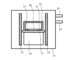
- FIG. 3 schematically shows a heating unit during nitriding in the present embodiment.
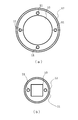
- FIG. 4 is a plan view showing the arrangement of the nitriding substrate and carbon in this embodiment.
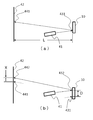
- FIG. 5 is a diagram schematically showing a method for measuring the radius of curvature of an alumina substrate in the present embodiment, where (a) shows a first measurement system as a reference, and (b) shows a state after the irradiation position is moved. An optical measurement system is shown.
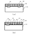
- FIGS. 6A and 6B are diagrams schematically showing a SEM observation of the backscattered electron image of the FIB processed cross section of the alumina substrate in the present embodiment.
- FIG. 6A is a cross section of the first embodiment, and FIG. Each of the cross sections is shown.
- the present invention is characterized in that a void and a rare earth-containing region are arranged in the AlN layer or at the interface between the AlN layer and the alumina substrate. The structure will be described with reference to FIG.
- the rare earth in this embodiment means each element of Y and lanthanide group. Since these elements have an ionic radius much larger than that of Al, they are highly effective as elements used in a region for concentrating stress.
- the rare earth element is characterized in that the structure of the present embodiment can be formed relatively easily, and since it is a high melting point material, it can withstand AlN crystal growth at a relatively high temperature.
- the rare earth element is not limited to one type, and a plurality of types of rare earth elements may be used simultaneously.
- FIG. 1 schematically shows a cross section of the alumina substrate of the present embodiment.
- FIG. 1A shows an example in which a void 31 and a rare earth-containing region 32 are formed inside the AlN layer 30 or at the interface between the alumina substrate 33 and the AlN layer 30.
- the individual voids 31 and the rare earth-containing region 32 may be arranged independently, or the adjacent voids 31 and the rare earth-containing region 32 may be in contact with each other.
- FIG. 1B shows an example in which the rare earth-containing region 32 is formed in layers, and the voids 31 are arranged so as to be in contact with or sandwiched between the layered rare earth-containing regions 32.
- the layered rare earth-containing region 32 is disposed inside the AlN layer 30 or at the interface between the alumina substrate 33 and the AlN layer 30.
- the stress caused by the lattice mismatch and the difference in thermal expansion coefficient between the alumina substrate 33 and the AlN layer 30 can be concentrated in the rare earth-containing region 32, and the rare earth is equivalent to the concentrated stress.
- the stress applied to the AlN layer 30 located closer to the surface than the containing region 32 can be reduced, and the warpage in the AlN layer 30 can be reduced. Further, since the stress is released even in the gap 31, the warp can be reduced. Furthermore, since cracks generated when excessive stress is applied during the growth of the AlN crystal are guided and propagated by the rare earth-containing region 32 and the voids 31, they can be separated from the alumina substrate without generating cracks or cracks in the grown crystal.
- the air gap 31 When the air gap 31 is arranged between the alumina substrate 33 and the AlN layer 30, the lattice mismatch between the alumina substrate 33 and the AlN layer 30 does not occur, so that warpage can be reduced. However, on the other hand, the strength of the entire alumina substrate 33 is reduced due to the formation of the air gap 31.
- an AlN crystal is grown using such a substrate, if the lattice mismatch stress generated as the crystal grows becomes excessive, cracks are generated and propagated through the gaps 31, and the grown crystal can be separated from the substrate. At the same time, however, too many voids 31 cause cracks and cracks even with a small stress such as handling, making them difficult to handle independently as a substrate. It was difficult to do.
- the inventors have found that by arranging the void and the rare earth-containing region in combination, the same effect as the void can be obtained and the substrate strength can be increased. Since the outermost surface layer of the alumina substrate of the present invention is the AlN layer 30, AlN crystals can be grown on the alumina substrate of the present invention with good consistency. In addition, when an excessive stress due to a lattice mismatch and a difference in thermal expansion coefficient occurs between the AlN crystal and the alumina substrate 33 as the AlN crystal grows, not only the voids formed in the alumina substrate of the present invention but also stress concentration. The rare earth-containing region 32 also causes cracks to propagate and propagate, and the grown crystal can be separated from the substrate without damaging the grown crystal.
- the rare earth-containing region 32 is lattice-bonded to the alumina substrate 33 and / or the AlN layer 30, it is possible to suppress a decrease in strength of the entire alumina substrate of the present invention. As a result, handling can be performed freely, and various processes can be performed as an independent substrate.
- the rare earth-containing region 32 and the voids 31 are desirably distributed along a plane substantially parallel to the alumina substrate surface 33s. This is because the generation and propagation of cracks that occur when an excessive stress is applied during AlN crystal growth is easily induced in a direction substantially parallel to the alumina substrate surface 33s, and it is easy to prevent cracks from entering the grown crystal. . Note that “substantially parallel” means that the difference in height that can suppress the propagation of cracks to the grown AlN crystal is an acceptable level of parallelism.
- the amount of rare earth element contained is 1 ppm or more and 10000 ppm or less, more preferably 1 ppm or more and 1000 ppm or less in terms of Al element ratio. Warpage can be remarkably reduced, and when an AlN crystal is grown on the alumina substrate of the present invention, cracks and cracks in the grown crystal can be prevented more remarkably.
- the layer thickness of the AlN layer 30 is 0.02 to 100 ⁇ m, preferably 0.05 to 10 ⁇ m, more preferably 0.2 to 1 ⁇ m. Warpage can be remarkably reduced, and when an AlN crystal is grown on the alumina substrate of the present invention, cracks and cracks in the grown crystal can be prevented more remarkably.
- the total length of the rare earth-containing regions 32 along the direction substantially parallel to the alumina substrate surface is preferably 10% or more and 100% or less with respect to the length in the direction substantially parallel to the alumina substrate surface.
- the total length of the gaps 31 along the direction substantially parallel to the alumina substrate surface is preferably 10% or more and 60% or less with respect to the length in the direction substantially parallel to the alumina substrate surface.
- the total length of the rare earth-containing region 32 and the gap 31 along the direction substantially parallel to the alumina substrate surface is preferably 50% or more and 100% or less with respect to the length in the direction substantially parallel to the alumina substrate surface.
- the thickness of the rare earth-containing region 32 and the void 31 in the direction perpendicular to the alumina substrate surface is preferably 50% or less with respect to the thickness of the AlN layer 30.
- the formed AlN layer 30 is mainly required to be a single crystal. Practically, it is desirable that 50% or more of the total area of the base substrate is single-crystallized. This can reduce the cost of manufacturing a device in which a semiconductor layer is stacked on a single crystal substrate such as a light emitting device or a power transistor.
- an alumina substrate having the same structure as that of this embodiment may be produced by another method.
- Fig. 2 illustrates the production flow.
- the main steps include a) a step of applying a rare earth-containing raw material to an alumina substrate, b) a drying step, c) a step of heat-treating the applied substrate in air, and d) a nitriding step. Further, this process may be repeated.
- a raw material containing the rare earth element is coated on an alumina substrate.
- the coating method is not particularly limited, and examples thereof include a vacuum method such as a sputtering method, a plating method, a spraying method, and a spin coating method.
- the coating was performed by spin coating. Since the spin coating method requires the use of a raw material solution, in this example, a rare earth nitrate ethanol solution and a rare earth MOD solution manufactured by High Purity Chemical Laboratory are used and spin coated at 1000 to 3000 rpm for 20 to 120 seconds to form a coating layer. Formed.
- the MOD solution is obtained by dissolving an organic salt of the rare earth element in a solution mainly composed of xylene.
- the heat treatment temperature is preferably 500 ° C. to 1400 ° C., more preferably 600 ° C. to 1000 ° C., although it depends on the type of rare earth-containing salt. In this temperature range, the smoothness of the substrate surface is maintained, and the coating solution can be completely thermally decomposed to be oxidized regardless of inorganic salt or organic salt.
- the substrate subjected to this treatment is used as the nitriding substrate 10.
- FIG. 3 schematically shows the heating part of the nitriding furnace.
- the heating furnace includes a carbon heater 22, a sample mounting table 20, and a chamber 23 that covers the whole.
- the chamber 23 is provided with a gas exhaust port 24 and a gas introduction port 25.
- the gas exhaust port 24 is connected to a rotary pump (not shown) and a diffusion pump (not shown), and has a structure that allows deaeration. It has become.
- nitrogen gas can be introduced through the gas inlet 25.
- An alumina plate 13 is placed on a sample mounting table, and a nitriding substrate 10 and carbon 11 are placed thereon.
- a substantially hermetic alumina pot 12 was placed on the alumina plate 13 so as to cover the entire nitriding substrate 10 and carbon 11.
- the substantially sealed shape means that the gas flow is not sufficiently sealed, but the gas tightness can be suppressed to some extent.
- the rare earth-containing raw material is disposed in the nitriding treatment, it is disposed so as to be covered with a substantially hermetic alumina sagger 12 like the carbon 11.
- the rare earth-containing raw material or carbon is adhered to the holding jig, it is applied to the inside of the alumina plate 13 or the substantially sealed alumina sagger 12.
- the heating temperature is about 1400-1800 ° C, although it depends on the type of rare earth element. If the temperature is lower than this, the formation of the AlN layer is not sufficient. On the other hand, if the temperature is too high, the alumina substrate as the processing substrate is deteriorated. At that time, carbon 11 is arranged in the vicinity of the substrate. The amount of carbon 11 varies depending on the processing size and processing conditions, and cannot be generally stated, but is 0.1 mg or more. If the amount is too small, the nitriding treatment cannot be performed sufficiently and AlN is not generated or becomes a very small amount. In addition, the crystallinity may be lowered.
- Carbon 11 was disposed around the nitriding substrate 10.
- This process forms the AlN layer 30 on the surface of the alumina substrate.
- the formed AlN layer 30 is formed by taking over the underlying substrate orientation. Since AlN is generated on the substrate surface even if Al is not included in the coating material, this AlN is not deposited on the surface of the alumina substrate, but oxygen in the alumina substrate in the vicinity of the surface is replaced with nitrogen to form AlN. It has been done. On the other hand, most of the rare earth applied to the substrate surface disappears by nitriding. It seems that nitrides or carbides are formed and gasified to disappear.
- the inventors have obtained a part of the rare earth element. We decided to leave it as an area and concentrate the lattice mismatch stress there. Therefore, we tried to leave some rare earths intentionally. As a result of trial and error, a part of the rare earth element can remain as a rare earth-containing region by adjusting the layer thickness and density of the rare earth-containing material to be applied, heat treatment temperature, nitriding treatment temperature, time and atmosphere control, and further the amount of carbon. Further, the inventors have found that a part of the gasified rare earth-containing material can be taken into the alumina substrate of this embodiment, and have completed the invention.
- the atmosphere is maintained in the closed heating furnace and the substantially sealed alumina sagger 12, but the present invention is not limited thereto. If the amount of carbon and the amount of rare earth elements can be controlled, it is possible to obtain an alumina substrate having the same structure as that of the present embodiment even with a gas flow or an open heating section.
- the warp can be evaluated by obtaining the radius of curvature by a method using surface reflected light. This will be described with reference to FIG.
- Light is irradiated from a visible LD or LED light source 41 to an arbitrary point 431 on the side where the AlN layer of the nitriding substrate 10 of this embodiment is formed, and the reflected light is imaged on the screen 42, and the result is The image position 441 is marked.
- FIG. 5A Subsequently, with the optical system fixed, the nitriding substrate 10 is moved by D in parallel with the screen, the irradiation position is changed to the position 432, and similarly the reflected light from the irradiation position 432 is reflected on the screen.
- the imaging position 442 that forms an image is marked.
- the distance between the two imaging positions 441 and 442 is defined as a displacement amount X. If the distance between the nitriding substrate 10 and the screen 42 is L and the curvature radius R of the warp of the nitriding substrate 10 is L and R are sufficiently larger than D and X, the curvature radius R is approximately expressed by the following equation. Can be sought.
- a MOD solution containing Y as a rare earth element with a concentration of 2 wt% was applied to a c-plane sapphire substrate having a size of 2 inches ⁇ by spin coating at 2000 rpm for 20 seconds. After coating, the film was dried on a hot plate at 150 ° C. for 10 minutes and then heat-treated in air at 600 ° C. for 2 hours. After heat treatment, it is placed on a 100 mm square alumina plate 13, and 20 mg of powdery carbon 11 is placed in four places around the substrate 10, and then the whole is placed in an alumina bowl 12 of 75 mm square and 70 mm height. After covering, the sample was placed on the sample setting table 20. This is shown in FIGS. 3 and 4 (a).
- the nitriding furnace is a resistance heating type electric furnace using carbon as a heater. Before heating, degassing was performed to 0.03 Pa using a rotary pump and a diffusion pump, and after flowing nitrogen gas to 100 kPa (atmospheric pressure), the flow of nitrogen gas was stopped.
- the nitriding treatment temperature was 1750 ° C.
- the treatment time was 12 hours
- the heating / cooling rate was 600 ° C./hour.
- the gas exhaust port 24 was appropriately opened and closed, and the pressure inside the chamber was adjusted to 250 kPa at the processing temperature. After cooling to room temperature, the treated substrate was taken out and evaluated.
- voids 31 were observed so as to be sandwiched between layered white areas 52 with respect to a 10 ⁇ m long visual field. All of the voids were substantially rectangular and each had a shape of 1.0 ⁇ m in length, 0.04 ⁇ m in thickness, 0.8 ⁇ m in length, and 0.04 ⁇ m in thickness.
- a direction parallel to the substrate surface is referred to as a length
- a direction perpendicular to the substrate surface is referred to as a thickness.
- the first crystal 50 was an AlN crystal, and the region 52 that glowed white contained an element having an atomic weight larger than that of the Al element from the properties of the reflected electron image.
- the element having an atomic weight larger than that of the Al element is considered to be Y, and it was confirmed by EPMA that it was Y.
- the first crystal 50 and the second crystal 53 were also subjected to elemental analysis by EPMA, and it was confirmed that the first crystal 50 was an AlN layer and the second crystal 53 was alumina.
- the rare earth-containing region 32 was 82%, the void 31 was 18%, and the total length of the rare earth-containing region 32 and the void 31 accounted for 100% with respect to the length direction of 10 ⁇ m. . Further, it was found that the rare earth-containing region 32 and the voids 31 were arranged substantially parallel to the substrate surface and had a thickness of 10% with respect to the thickness of the AlN layer 30. ⁇ Example 2>
- Example 1 In the 10 mm square sample cut out in Example 1, XRD measurement, SEM observation, and EPMA measurement were performed using a sample near the outer periphery.
- XRD measurement a diffraction line of AlN (002) was recognized as in Example 1, and the intensity ratio of the AlN (002) diffraction line to the sapphire (006) diffraction line was 55%.
- the polar measurement using the (112) plane six peaks corresponding to the six-fold axis appeared, and it was confirmed that it was a single crystal.
- the radius of curvature was 110 m, and X-ray fluorescence analysis detected 180 ppm of Y atoms relative to the number of Al atoms. Compared to Example 1, it can be seen that as the rare earth content increases, the radius of curvature increases, that is, the warp decreases.
- FIG. 6B schematically shows the result of SEM reflection electron image observation.
- a white shining region 52 and voids 31 were observed in the interface between the first crystal 50 and the second crystal 53 having a thickness of 0.5 ⁇ m and in the first crystal 50 in the vicinity of the interface.
- Three white shining regions 52 were not layered, and three regions were observed in an independent form for a 10 ⁇ m long field of view.
- the maximum length was 1 ⁇ m and the minimum was 0.4 ⁇ m. All the thicknesses were 0.02 ⁇ m.
- five voids 31 were observed.
- the length of the gap 31 was 1 ⁇ m at the maximum and 0.2 ⁇ m at the minimum.
- the thickness was 0.4 ⁇ m at the maximum and 0.1 ⁇ m at the minimum.
- the shape was substantially rectangular and substantially triangular.
- a direction parallel to the substrate surface is referred to as a length
- a direction perpendicular to the substrate surface is referred to as a thickness.
- the region 52 that glows white was found to be the rare earth-containing region 32 by the same estimation and confirmation as in Example 1. As a result of SEM observation, it was found that the rare earth-containing region 32 accounted for 28%, the voids 31 accounted for 25%, and the total of the rare earth-containing regions 32 and the voids 31 accounted for 53% with respect to the length direction of 10 ⁇ m. Further, it was found that the rare earth-containing region 32 and the voids 31 were arranged substantially parallel to the substrate surface and had a thickness of 8% at the maximum with respect to the thickness of the AlN layer 30.
- Example 3 One of 10 mm square samples cut out from the vicinity of the central portion as in Example 1 was used as a substrate, and an AlN single crystal was grown by a flux method.
- the flux method is under the following conditions. Materials (composition: Si 35.7 wt%, C 2.3 wt%, Al 62.0 wt% weight: 150 g) were put in a yttria-stabilized zirconia crucible and placed in a heating region of a high-frequency heating furnace. A stirring jig made of yttria-stabilized zirconia to which a nitrided sapphire substrate was fixed was disposed immediately above the material. After melting the material temperature up to 1600 ° C.
- the solution was saturated with nitrogen by holding the solution with a stirring blade for 5 hours while stirring. Thereafter, while the nitrided sapphire substrate was brought into contact with the solution surface and rotated at 100 rpm, the material temperature was gradually lowered to grow an AlN single crystal on the sapphire substrate over 20 hours. After crystal growth was completed, the sapphire substrate was removed from the solution and the material was cooled to room temperature. When the sample was taken out from the furnace after completion of cooling, the alumina substrate was peeled off in the lateral direction, and the AlN single crystal plate was separated from the sapphire substrate portion. It seems that the rare earth-containing region was naturally exfoliated as a result of concentrated stress due to lattice mismatch during the growth of the AlN crystal. The thickness of the AlN single crystal plate was 250 ⁇ m. ⁇ Example 4>
- Example 5 One of 10 mm square samples cut out from the vicinity of the outer periphery similar to Example 2 was used as a substrate, and AlN single crystal was grown by a flux method.
- the conditions of the flux method are the same as in Example 3.
- the sample was taken out from the furnace after completion of cooling, the alumina substrate was peeled off in the lateral direction, and the AlN single crystal plate was separated from the sapphire substrate portion. It seems that the rare earth-containing region was naturally exfoliated as a result of concentrated stress due to lattice mismatch during the growth of the AlN crystal.
- the thickness of the AlN single crystal plate was 250 ⁇ m.
- C-plane sapphire was cut into 10 mm square to prepare a substrate 10 for nitriding treatment.
- a surfactant was added to prepare a coating solution.
- Spin coating was performed at 3000 rpm for 20 seconds.
- heat treatment was performed in air at 600 ° C. for 2 hours. After the heat treatment, it was placed on a 100 mm square alumina plate 13, and 500 mg of block-like carbon 11 was further placed at two sides of the substrate 10.
- the layout is shown in FIG.
- a substantially sealed alumina bowl 12 a cylindrical alumina crucible having a diameter of 30 mm and a height of 30 mm is used, and the alumina crucible is inverted so as to cover the substrate 10 and the block-shaped carbon 11 to obtain a substantially sealed state. It was realized.
- the nitriding treatment was performed in the same manner as in Example 1.
- the first crystal 50 has a thickness of 0.15 ⁇ m, and a white shining region 52 having a thickness of about 0.02 ⁇ m was observed in layers.
- four voids having a length of about 0.5 ⁇ m and a thickness of about 0.02 ⁇ m were observed in a field of view of 10 ⁇ m so as to be sandwiched between the layered white glowing regions 52.
- Nd atoms were 100 ppm in terms of the number of Al atoms, and the radius of curvature was 77 m. From the results of XRD measurement, SEM observation and EPMA, it was confirmed that the first crystal 50 was an AlN layer, the second crystal 53 was alumina, and that the layered white glowing region 52 contained Nd.
- Example 1 A sapphire (006) diffraction line was obtained when the same treatment as in Example 5 was performed except that a cylindrical alumina crucible having a diameter of 60 mm and a height of 50 mm was used as the alumina mortar 12 and that the pressure in the chamber was 10 kPa.
- the intensity ratio of the AlN (002) diffraction line to 15% was 15%, and the thickness of the first crystal 50 was 0.12 ⁇ m. The thickness of was thin.
- the radius of curvature was 15 m, Nd was not detected, and no voids were observed. From the comparison between Example 5 and Comparative Example 1, it can be seen that the inclusion of rare earth and voids increases the radius of curvature of the alumina substrate of the present embodiment, that is, reduces warpage.
- C-plane sapphire was cut into 10 mm square to prepare a substrate 10 for nitriding treatment.
- a MOD solution containing Eu as a rare earth element having a concentration of 2 wt% was applied by spin coating at 2000 rpm for 20 seconds. After coating, the film was dried on a hot plate at 150 ° C. for 10 minutes and then heat-treated in air at 600 ° C. for 2 hours.
- the nitriding treatment was performed in the same manner as in Example 5. However, the processing temperature was 1600 ° C.
- the thickness of the first crystal 50 is 0.2 ⁇ m, and a white shining region 52 appears in a layer shape, the thickness is about 0.02 ⁇ m, and the layered white shining region 52. It was confirmed that two voids having a length of about 0.8 ⁇ m to 1.5 ⁇ m and a thickness of about 0.02 ⁇ m were observed in a 10 ⁇ m long visual field.
- the radius of curvature was 35 m, and Eu atoms were 50 ppm in terms of the number of Al atoms. From the results of XRD measurement, SEM observation, and EPMA, it was confirmed that the first crystal 50 was an AlN layer, the second crystal 53 was alumina, and that the white glowing region 52 contained Eu.
- the alumina substrate of the present invention can be used not only as a substrate for growing a single crystal such as AlN but also as a substrate for light emitting elements and semiconductor elements, or a product in a field using the high thermal conductivity of AlN. It is.
- the alumina substrate itself of the present invention can be used directly as long as it does not impair the industrial utility value. That is, as long as the amount of the rare earth contained is in an allowable range, it can be used as a high thermal conductivity substrate, a surface acoustic wave substrate, or a piezoelectric substrate.
Landscapes
- Chemical & Material Sciences (AREA)
- Engineering & Computer Science (AREA)
- Crystallography & Structural Chemistry (AREA)
- Materials Engineering (AREA)
- Metallurgy (AREA)
- Organic Chemistry (AREA)
- Inorganic Chemistry (AREA)
- Chemical Kinetics & Catalysis (AREA)
- General Chemical & Material Sciences (AREA)
- Dispersion Chemistry (AREA)
- Crystals, And After-Treatments Of Crystals (AREA)
Abstract
Description
なお照射位置431を起点とした照射位置432の変位ベクトルと結像位置441を起点とした結像位置442の変位ベクトルが平行であれば凸、反平行であれば凹となっている。
<実施例1>
<実施例2>
実施例1と同様の中心部付近から切り出した10mm角の試料の中の1つを基板とし、フラックス法にてAlN単結晶育成を行った。フラックス法は以下の条件である。イットリア安定化ジルコニア製ルツボに材料(組成:Si35.7wt%、C2.3wt%、Al62.0wt% 重量:150g)を入れて、高周波加熱炉の加熱領域に置いた。材料直上には窒化処理したサファイア基板を固定したイットリア安定化ジルコニア製の撹拌治具を配置した。窒素雰囲気中で材料温度を1600℃まで上げて溶融させた後、撹拌羽根で溶液を撹拌しながら5時間保持して溶液を窒素で飽和させた。その後窒化処理したサファイア基板を溶液表面に接触させて100rpmで回転させながら、材料温度を徐々に下げてサファイア基板上にAlN単結晶を20時間かけて成長させた。結晶成長が終了した後、サファイア基板を溶液から離し材料を室温まで冷やした。冷却終了後炉内から試料を取り出したところ、アルミナ基板が横方向に剥離し、AlN単結晶板がサファイア基板の部分から分離していた。AlN結晶の育成中に希土類含有領域が格子不整合による応力を集中して受けた結果、自然剥離したと思われる。AlN単結晶板の厚さは250μmであった。
<実施例4>
<実施例5>
直径60mm、高さ50mmの円筒状アルミナルツボをアルミナ匣鉢12として用いたこと、およびチャンバー内圧力を10kPaとしたこと以外は実施例5と同様な処理を行ったところ、サファイア(006)回折線に対するAlN(002)回折線の強度比は15%、第一の結晶50の厚さは0.12μmと実施例5と比較すると、AlN(002)回折線強度が減少し、また第一の結晶の厚さが薄くなっていた。一方、曲率半径は15m、またNdは検出されず、更に空隙も観察されなかった。実施例5と比較例1との比較から、希土類と空隙を含有することにより、本実施形態のアルミナ基板の曲率半径が大きくなる、即ちソリが小さくなっていることがわかる。
<実施例6>
11 カーボン
12 アルミナ匣鉢
13 アルミナ板
20 試料設置台
22 カーボンヒーター
23 チャンバー
24 ガス排気口
25 ガス導入口
30 AlN層
31 空隙
32 希土類含有領域
33 アルミナ基板
33s アルミナ基板表面
41 可視のLD、またはLED光源
42 スクリーン
431 本実施形態の窒化処理基板10のAlN層が形成されている側の任意の一点における光の照射位置
432 本実施形態の窒化処理基板10をスクリーン42と平行に移動した後の光の照射位置
441 光の照射位置431に対応してスクリーン上に結像した反射光の結像位置
442 光の照射位置432に対応してスクリーン上に結像した反射光の結像位置
50 第一の結晶
52 白く光る領域
53 第二の結晶
Claims (5)
- アルミナ基板であって、前記アルミナ基板表面にはAlN層が形成されており、かつ前記AlN層の内部または前記AlN層と前記アルミナ基板界面に希土類含有領域および空隙が形成されていることを特徴とするアルミナ基板。
- 希土類含有量がAl元素比で1~10000ppmであることを特徴とする請求項1記載のアルミナ基板。
- 前記AlN層の厚さが0.02μmから100μmであることを特徴とする請求項1または請求項2記載のアルミナ基板。
- 前記アルミナ基板はサファイアであることを特徴とする請求項1~請求項3のいずれか一項に記載のアルミナ基板。
- 前記AlN層は主として単結晶であることを特徴とする請求項4記載のアルミナ基板。
Priority Applications (3)
| Application Number | Priority Date | Filing Date | Title |
|---|---|---|---|
| KR1020177022339A KR102025617B1 (ko) | 2015-03-23 | 2016-03-02 | 알루미나 기판 |
| US15/554,109 US10458041B2 (en) | 2015-03-23 | 2016-03-02 | Alumina substrate |
| CN201680011843.9A CN107532330B (zh) | 2015-03-23 | 2016-03-02 | 氧化铝基板 |
Applications Claiming Priority (2)
| Application Number | Priority Date | Filing Date | Title |
|---|---|---|---|
| JP2015-059234 | 2015-03-23 | ||
| JP2015059234A JP6503819B2 (ja) | 2015-03-23 | 2015-03-23 | アルミナ基板 |
Publications (1)
| Publication Number | Publication Date |
|---|---|
| WO2016152422A1 true WO2016152422A1 (ja) | 2016-09-29 |
Family
ID=56977287
Family Applications (1)
| Application Number | Title | Priority Date | Filing Date |
|---|---|---|---|
| PCT/JP2016/056431 Ceased WO2016152422A1 (ja) | 2015-03-23 | 2016-03-02 | アルミナ基板 |
Country Status (5)
| Country | Link |
|---|---|
| US (1) | US10458041B2 (ja) |
| JP (1) | JP6503819B2 (ja) |
| KR (1) | KR102025617B1 (ja) |
| CN (1) | CN107532330B (ja) |
| WO (1) | WO2016152422A1 (ja) |
Families Citing this family (3)
| Publication number | Priority date | Publication date | Assignee | Title |
|---|---|---|---|---|
| KR102244833B1 (ko) | 2019-12-10 | 2021-04-27 | 주식회사 유텔 | 적층형 lcp 전자소자 |
| WO2021131967A1 (ja) * | 2019-12-23 | 2021-07-01 | 日本碍子株式会社 | AlN積層板 |
| WO2021182107A1 (ja) * | 2020-03-11 | 2021-09-16 | 昭和電工株式会社 | 耐食性部材 |
Citations (4)
| Publication number | Priority date | Publication date | Assignee | Title |
|---|---|---|---|---|
| WO2009031696A1 (ja) * | 2007-09-04 | 2009-03-12 | Ube Industries, Ltd. | 発光素子形成用複合基板及びその製造方法 |
| WO2009066663A1 (ja) * | 2007-11-22 | 2009-05-28 | Meijo University | 窒化アルミニウム単結晶多角柱状体及びそれを使用した板状の窒化アルミニウム単結晶の製造方法 |
| WO2011004601A1 (ja) * | 2009-07-07 | 2011-01-13 | 株式会社ユメックス | 蛍光体結晶薄膜とその作製方法 |
| WO2016024514A1 (ja) * | 2014-08-12 | 2016-02-18 | Tdk株式会社 | アルミナ基板 |
Family Cites Families (12)
| Publication number | Priority date | Publication date | Assignee | Title |
|---|---|---|---|---|
| JPS5324110A (en) | 1976-08-18 | 1978-03-06 | Hitachi Ltd | Automatic valve of reciprocating commpressor |
| US6627974B2 (en) * | 2000-06-19 | 2003-09-30 | Nichia Corporation | Nitride semiconductor substrate and method for manufacturing the same, and nitride semiconductor device using nitride semiconductor substrate |
| DE10393690T5 (de) * | 2002-11-29 | 2005-09-15 | Sumitomo Chemical Co., Ltd. | III-V Halbleiter und Verfahren zur seiner Herstellung |
| JP4457576B2 (ja) | 2003-05-08 | 2010-04-28 | 住友電気工業株式会社 | Iii−v族化合物結晶およびその製造方法 |
| KR100921789B1 (ko) * | 2007-10-24 | 2009-10-15 | 주식회사 실트론 | 화합물 반도체 기판 제조 방법 |
| JP5324110B2 (ja) * | 2008-01-16 | 2013-10-23 | 国立大学法人東京農工大学 | 積層体およびその製造方法 |
| JP5307671B2 (ja) * | 2008-10-23 | 2013-10-02 | 日本碍子株式会社 | 窒化アルミニウム基複合材料、その製造方法及び半導体製造装置用部材 |
| JP5277270B2 (ja) * | 2010-07-08 | 2013-08-28 | 学校法人立命館 | 結晶成長方法および半導体素子 |
| TWI617045B (zh) * | 2012-07-06 | 2018-03-01 | Epistar Corporation | 具有奈米柱之發光元件及其製造方法 |
| US9000415B2 (en) * | 2012-09-12 | 2015-04-07 | Lg Innotek Co., Ltd. | Light emitting device |
| JP5896470B2 (ja) * | 2012-11-16 | 2016-03-30 | 国立大学法人名古屋大学 | AlN単結晶の製造方法 |
| KR102232265B1 (ko) * | 2014-07-14 | 2021-03-25 | 주식회사 헥사솔루션 | 기판 구조, 그 형성방법, 및 이를 이용한 질화물 반도체 제조방법 |
-
2015
- 2015-03-23 JP JP2015059234A patent/JP6503819B2/ja not_active Expired - Fee Related
-
2016
- 2016-03-02 US US15/554,109 patent/US10458041B2/en active Active
- 2016-03-02 KR KR1020177022339A patent/KR102025617B1/ko not_active Expired - Fee Related
- 2016-03-02 WO PCT/JP2016/056431 patent/WO2016152422A1/ja not_active Ceased
- 2016-03-02 CN CN201680011843.9A patent/CN107532330B/zh not_active Expired - Fee Related
Patent Citations (4)
| Publication number | Priority date | Publication date | Assignee | Title |
|---|---|---|---|---|
| WO2009031696A1 (ja) * | 2007-09-04 | 2009-03-12 | Ube Industries, Ltd. | 発光素子形成用複合基板及びその製造方法 |
| WO2009066663A1 (ja) * | 2007-11-22 | 2009-05-28 | Meijo University | 窒化アルミニウム単結晶多角柱状体及びそれを使用した板状の窒化アルミニウム単結晶の製造方法 |
| WO2011004601A1 (ja) * | 2009-07-07 | 2011-01-13 | 株式会社ユメックス | 蛍光体結晶薄膜とその作製方法 |
| WO2016024514A1 (ja) * | 2014-08-12 | 2016-02-18 | Tdk株式会社 | アルミナ基板 |
Also Published As
| Publication number | Publication date |
|---|---|
| US20180038011A1 (en) | 2018-02-08 |
| KR102025617B1 (ko) | 2019-09-27 |
| CN107532330A (zh) | 2018-01-02 |
| JP2016175816A (ja) | 2016-10-06 |
| CN107532330B (zh) | 2020-08-07 |
| US10458041B2 (en) | 2019-10-29 |
| KR20170106375A (ko) | 2017-09-20 |
| JP6503819B2 (ja) | 2019-04-24 |
Similar Documents
| Publication | Publication Date | Title |
|---|---|---|
| JP6418343B2 (ja) | アルミナ基板の製造方法 | |
| Nahhas et al. | Epitaxial growth of ZnO films on Si substrates using an epitaxial GaN buffer | |
| US20130040442A1 (en) | METHOD OF MANUFACTURING GaN-BASED FILM | |
| CN103814160A (zh) | 复合基板、其制造方法、13族元素氮化物构成的功能层的制造方法以及功能元件 | |
| JP6503819B2 (ja) | アルミナ基板 | |
| US20150118830A1 (en) | Method of Manufacturing GaN-Based Film and Composite Substrate Used Therefor | |
| JP2021109805A (ja) | Iii族窒化物基板の製造方法及びiii族窒化物基板 | |
| JP2011246749A (ja) | アルミニウム系iii族窒化物製造装置、およびアルミニウム系iii族窒化物の製造方法 | |
| JP2019064870A (ja) | 複合基板 | |
| Shervin et al. | Flexible single-crystalline GaN substrate by direct deposition of III-N thin films on polycrystalline metal tape | |
| JP6394170B2 (ja) | アルミナ基板 | |
| CN114144864A (zh) | Iii族化合物基板的制造方法和利用该制造方法制造的基板 | |
| Sha et al. | Structure and optical properties of the SiC/ZnO five-layer multi-layer on Si (111) substrate with a SiC buffer layer | |
| US20220235489A1 (en) | Method for manufacturing group iii compound substrate, and group iii compound substrate | |
| CN109637925B (zh) | 氧化镁锌薄膜及其制备方法 | |
| TW202331794A (zh) | 氮化物半導體基板及氮化物半導體基板的製造方法 | |
| KR101195473B1 (ko) | 질화갈륨 성장방법 | |
| JP2020031175A (ja) | 積層体及び積層体の製造方法 |
Legal Events
| Date | Code | Title | Description |
|---|---|---|---|
| 121 | Ep: the epo has been informed by wipo that ep was designated in this application |
Ref document number: 16768325 Country of ref document: EP Kind code of ref document: A1 |
|
| ENP | Entry into the national phase |
Ref document number: 20177022339 Country of ref document: KR Kind code of ref document: A |
|
| WWE | Wipo information: entry into national phase |
Ref document number: 15554109 Country of ref document: US |
|
| NENP | Non-entry into the national phase |
Ref country code: DE |
|
| 122 | Ep: pct application non-entry in european phase |
Ref document number: 16768325 Country of ref document: EP Kind code of ref document: A1 |