WO2016151861A1 - 液晶表示装置 - Google Patents
液晶表示装置 Download PDFInfo
- Publication number
- WO2016151861A1 WO2016151861A1 PCT/JP2015/059489 JP2015059489W WO2016151861A1 WO 2016151861 A1 WO2016151861 A1 WO 2016151861A1 JP 2015059489 W JP2015059489 W JP 2015059489W WO 2016151861 A1 WO2016151861 A1 WO 2016151861A1
- Authority
- WO
- WIPO (PCT)
- Prior art keywords
- liquid crystal
- display device
- crystal display
- slits
- slit
- Prior art date
- Legal status (The legal status is an assumption and is not a legal conclusion. Google has not performed a legal analysis and makes no representation as to the accuracy of the status listed.)
- Ceased
Links
Images











Classifications
-
- G—PHYSICS
- G02—OPTICS
- G02F—OPTICAL DEVICES OR ARRANGEMENTS FOR THE CONTROL OF LIGHT BY MODIFICATION OF THE OPTICAL PROPERTIES OF THE MEDIA OF THE ELEMENTS INVOLVED THEREIN; NON-LINEAR OPTICS; FREQUENCY-CHANGING OF LIGHT; OPTICAL LOGIC ELEMENTS; OPTICAL ANALOGUE/DIGITAL CONVERTERS
- G02F1/00—Devices or arrangements for the control of the intensity, colour, phase, polarisation or direction of light arriving from an independent light source, e.g. switching, gating or modulating; Non-linear optics
- G02F1/01—Devices or arrangements for the control of the intensity, colour, phase, polarisation or direction of light arriving from an independent light source, e.g. switching, gating or modulating; Non-linear optics for the control of the intensity, phase, polarisation or colour
- G02F1/13—Devices or arrangements for the control of the intensity, colour, phase, polarisation or direction of light arriving from an independent light source, e.g. switching, gating or modulating; Non-linear optics for the control of the intensity, phase, polarisation or colour based on liquid crystals, e.g. single liquid crystal display cells
- G02F1/133—Constructional arrangements; Operation of liquid crystal cells; Circuit arrangements
- G02F1/1333—Constructional arrangements; Manufacturing methods
- G02F1/1337—Surface-induced orientation of the liquid crystal molecules, e.g. by alignment layers
-
- G—PHYSICS
- G02—OPTICS
- G02F—OPTICAL DEVICES OR ARRANGEMENTS FOR THE CONTROL OF LIGHT BY MODIFICATION OF THE OPTICAL PROPERTIES OF THE MEDIA OF THE ELEMENTS INVOLVED THEREIN; NON-LINEAR OPTICS; FREQUENCY-CHANGING OF LIGHT; OPTICAL LOGIC ELEMENTS; OPTICAL ANALOGUE/DIGITAL CONVERTERS
- G02F1/00—Devices or arrangements for the control of the intensity, colour, phase, polarisation or direction of light arriving from an independent light source, e.g. switching, gating or modulating; Non-linear optics
- G02F1/01—Devices or arrangements for the control of the intensity, colour, phase, polarisation or direction of light arriving from an independent light source, e.g. switching, gating or modulating; Non-linear optics for the control of the intensity, phase, polarisation or colour
- G02F1/13—Devices or arrangements for the control of the intensity, colour, phase, polarisation or direction of light arriving from an independent light source, e.g. switching, gating or modulating; Non-linear optics for the control of the intensity, phase, polarisation or colour based on liquid crystals, e.g. single liquid crystal display cells
- G02F1/133—Constructional arrangements; Operation of liquid crystal cells; Circuit arrangements
- G02F1/1333—Constructional arrangements; Manufacturing methods
- G02F1/1343—Electrodes
Definitions
- the present invention relates to a liquid crystal display device provided in a television receiver, a personal computer or the like.
- the liquid crystal display device is thin and has low power consumption.
- the display panel of the liquid crystal display device has a color filter (CF) substrate, a liquid crystal layer, an active matrix substrate (TFT substrate), and two polarizing plates.
- the CF substrate and the active matrix substrate are bonded to each other with a sealing material interposed therebetween, and a liquid crystal layer is formed with liquid crystal interposed therebetween.
- the active matrix substrate has a pixel electrode on the liquid crystal layer side, and the CF substrate has a common electrode on the liquid crystal layer side.
- the two polarizing plates are arranged on the surfaces of the CF substrate and the active matrix substrate opposite to the liquid crystal layer side.
- a liquid crystal display device using a vertical alignment material as a liquid crystal material is called a VA (Vertical Alignment) mode liquid crystal display device.
- VA Vertical Alignment
- an alignment division structure in which a plurality of liquid crystal domains are formed in one pixel is employed.
- MVA Multi-domain / Vertical / Alignment
- an alignment regulation structure is obtained by providing linear protrusions on the liquid crystal layer side of the substrate sandwiching the liquid crystal layer, or by providing openings (slits) in the pixel electrodes.
- Liquid crystal domains are formed (for example, Patent Document 1). By making the slits finer, the orientation of the liquid crystal molecules can be controlled more and the transmittance and response speed are improved.
- An alignment film such as a photo-alignment film is provided on the liquid crystal layer side of both substrates facing each other across the liquid crystal layer so that the pretilt direction (alignment processing direction) is orthogonal to each other, and the liquid crystal molecules are twisted when a voltage is applied.
- the VA mode configured as described above is called a VATN (Vertical / Alignment / Twisted / Nematic) mode (for example, Patent Document 2).
- a structure in which four liquid crystal domains divided into two rows and two columns are formed when a voltage is applied by defining the pretilt direction with two alignment films in one pixel region is called a 4D structure.
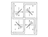
- FIG. 18 is a plan view showing a pixel region of a VATN mode liquid crystal display device having this 4D structure.
- the dotted arrow indicates the pretilt direction defined by the photoalignment film provided on the active matrix substrate
- the solid arrow indicates the pretilt direction defined by the photoalignment film provided on the CF substrate.
- the tilt direction (reference alignment direction) of each liquid crystal domain when a voltage is applied to the liquid crystal layer is indicated by the pin direction. It shows that the liquid crystal molecules are tilted so that the disk portion (head) of the pin is close to the viewer of the liquid crystal display device. That is, the reference orientation direction is oblique 45 °. No slit is formed in the pixel electrode of this liquid crystal display device.
- FIG. 19 is a plan view showing the light transmission state of the pixel region of FIG. 18, and FIG. 20 is an enlarged view of the upper right portion (liquid crystal domain B portion) of FIG. 19 and 20 show a state in which wirings and contact holes are arranged.
- the contact hole is formed at the center of the pixel region.
- the alignment of the liquid crystal molecules is indicated by pins. 19 and 20, it can be seen that a dark line having a wide width is generated on the outer side of the pixel region and the boundary of the liquid crystal domain.
- the liquid crystal molecules are tilted in an inward direction perpendicular to the outer side, and in the vicinity of the outer side of the pixel region, the liquid crystal molecules tilted in the outer side and the liquid crystal molecules aligned in the tilt direction
- the heads of the liquid crystal molecules face each other, the orientation of the liquid crystal molecules is disturbed, and the liquid crystal molecules are bent in a direction perpendicular or parallel to the polarization axis, so that a region where light is not transmitted is generated.
- the tilt angle differs by 90 ° on both sides of the boundary, so the liquid crystal molecules are bent and aligned in a direction perpendicular to the boundary (a direction perpendicular or parallel to the polarization axis), and a wide area where light is not transmitted. Occurs.
- the transmittance decreases due to the dark line. In particular, in a high-definition display with small pixels, the influence of a decrease in transmittance due to dark lines becomes large.
- FIG. 21 is a plan view showing pixel electrodes of the active matrix substrate in the pixel region of the liquid crystal display device of Patent Document 3.
- FIG. 21 In each liquid crystal domain of the pixel electrode, a plurality of slits extending in the direction perpendicular to the outer side of the pixel region are arranged in parallel.
- the slit group is provided corresponding to the dark line generated on the outer side of the pixel region, thereby controlling the orientation of liquid crystal molecules and increasing the transmittance.
- FIG. 22 is a plan view showing a light transmission state when wiring and contact holes are arranged in the pixel region of FIG. 21, and FIG. 23 is an enlarged view of a portion of the liquid crystal domain B of FIG. From FIG. 22, it can be seen that a dark line is generated at the inner end of the slit group surrounded by an ellipse. This is because, as shown in FIG. 23, the alignment of the liquid crystal molecules is disturbed at the slit break, and the liquid crystal molecules collide and bend in the direction in which the ends of the slit are aligned, that is, in the direction perpendicular or parallel to the polarization axis. This is because a region where light cannot be transmitted is generated.
- the present invention has been made in view of such circumstances, and provides a liquid crystal display device having a small area of dark lines generated when light is transmitted to a pixel region, good light transmittance, and good image quality.
- the purpose is to do.
- the liquid crystal display device includes an electrode and a photo-alignment film formed on one surface in order, and includes two substrates facing each other and a vertically-aligned liquid crystal material, and a liquid crystal interposed between both photo-alignment films A layer, a plurality of pixel regions formed in a matrix in the surface direction of the substrate on the substrate, and a reference alignment direction that is included in each pixel region and defined by both photo-alignment films is different, at least 2
- a liquid crystal display device having one liquid crystal domain and a plurality of openings formed in a region corresponding to each liquid crystal domain of one electrode and extending in parallel with each reference alignment direction, each opening in each liquid crystal domain One end of the opening is formed so as to be aligned in a direction crossing the reference orientation direction.
- the liquid crystal molecules are provided so as to be aligned along the direction in which the opening extends (reference alignment direction), and one end thereof is arranged in a direction crossing the reference alignment direction.
- the molecular orientation is not disturbed. Since the liquid crystal molecules are oriented in a plurality of directions at the opening cuts, when the ends are not aligned between the openings, the liquid crystal molecules in the adjacent openings interfere with each other on the end side and are bent to be perpendicular to the polarization axis or Oriented in parallel directions, dark lines occur. In the present embodiment, interference between adjacent liquid crystal molecules on the end side is suppressed.
- the area of the dark line generated when light is transmitted to the pixel region is small, the light transmittance is good, and the image quality is good.
- the openings are arranged in a direction perpendicular or parallel to the polarization axis as in the conventional liquid crystal display device of FIG. 21, even if the ends of the openings are aligned as shown in FIG. Since the molecules are aligned in the reference alignment direction, the liquid crystal molecules in the opening adjacent to each other on the end side interfere with each other, and the direction is bent in a direction perpendicular or parallel to the polarization axis.
- the liquid crystal display device according to the present invention is characterized in that the other end of each opening is also formed in a straight line.
- the other end of the opening is also arranged in a straight line, the alignment of liquid crystal molecules is not disturbed, and the generation of dark lines is further suppressed.
- the liquid crystal display device is characterized in that the opening has a linear portion extending in a direction perpendicular to the outer side of the pixel region.
- the width of the dark line generated on the outer side becomes narrow. This is because the liquid crystal molecules present in the gap between the end of the linear portion and the outer side are pushed and bent by the liquid crystal molecules arranged along the end and the outer side, in a direction parallel to the outer side, This is considered to be because they are arranged in a narrow area.
- the liquid crystal display device according to the present invention is characterized in that a length of the linear portion is 10 ⁇ m or more and less than 20 ⁇ m.
- an angle formed between a straight line connecting one end of each opening and the outer side is approximately 45 degrees, a portion extending in parallel with a reference alignment direction of each opening, and the line
- An angle formed by a straight line connecting a boundary portion with the shape portion and the outer side is approximately 22.5 degrees.
- the linear portion can be well connected to the portion extending in parallel with the reference orientation direction without changing the width.
- the liquid crystal display device is configured such that light is transmitted through the two substrates, and the opening is an end of the liquid crystal molecule on the light emission side at the center in the thickness direction of the liquid crystal layer. It is provided on the facing side.
- the openings are intensively provided in the portion where the dark line is generated when there is no opening, the generation of the dark line is suppressed satisfactorily. And since the portion where the opening is provided is limited, when the liquid crystal display device is configured as a touch panel, the recovery from the disorder of the alignment of the liquid crystal molecules due to finger pressing is accelerated, and unevenness is suppressed. Has been.
- each opening extending parallel to each reference alignment direction is formed so that one end thereof is aligned in a direction crossing each reference alignment direction.
- the direction parallel to the reference orientation direction is not disturbed, and the generation of dark lines is suppressed. Therefore, in the liquid crystal display device according to the present invention, the area of the dark line generated when light is transmitted to the pixel region is small, the light transmittance is good, and the image quality is good.
- FIG. 1 is an external perspective view of a liquid crystal display device according to Embodiment 1 of the present invention.
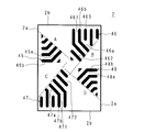
- FIG. 3 is a plan view showing pixel electrodes in one pixel region of the display panel of the liquid crystal display device according to Embodiment 1 of the present invention.
- FIG. 3 is a cross-sectional view of the display module taken along line III-III in FIG. It is a top view which shows the wiring of an active matrix substrate.
- FIG. 3 is a plan view showing a light transmission state in the pixel region of FIG. 2.
- FIG. 6 is an enlarged view showing an upper right part (part of liquid crystal domain B) of FIG. 5. It is a top view which shows the pixel electrode in one pixel area of the display panel which concerns on Embodiment 2 of this invention.
- FIG. 16 is a plan view showing a light transmission state in the pixel region of FIG. 15. It is a top view which shows the pixel electrode in one pixel area of the display panel which concerns on Embodiment 6 of this invention. It is a top view which shows the pixel area
- FIG. FIG. 20 is an enlarged view of a portion of the liquid crystal domain B in FIG. 19.
- FIG. 10 is a plan view showing pixel electrodes of an active matrix substrate in a pixel region of a liquid crystal display device of Patent Document 3.
- FIG. FIG. 22 is a plan view showing a light transmission state when wiring and contact holes are arranged in the pixel region of FIG. 21. It is an enlarged view of the part of the liquid crystal domain B of FIG.
- FIG. 1 is an external perspective view of a liquid crystal display device 100 according to Embodiment 1 of the present invention
- FIG. 2 is a plan view showing a pixel electrode 2 in one pixel region of a display panel 102 of the liquid crystal display device 100
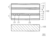
- FIG. FIG. 4 is a sectional view of the display module 101 taken along line III-III, and FIG.
- the liquid crystal display device 100 includes a display module 101 having a display panel 102 and a backlight unit 103, a synthetic resin front cabinet 104 and rear cabinet 105 that are accommodated so as to sandwich the display module 101, and a stand 106.
- the display module 101 has a horizontally long substantially rectangular parallelepiped shape as a whole, and is housed in the front cabinet 104 and the rear cabinet 105 in a vertical posture.
- the display panel 102 according to Embodiment 1 has a plurality of pixel regions arranged in a matrix in the surface direction.
- the display panel 102 is a multi-domain VATN mode display panel. As shown in FIG. 2, the four liquid crystal domains A, B, C, and D of the pixel electrode 2 of the active matrix substrate 1 have rounded rectangular shapes. None, a group of slits 21, slits 22, slits 23, and slits 24 extending corresponding to the 45 ° tilt direction of each liquid crystal domain are formed.
- the slit 21 is on the side of the liquid crystal domain A where the head of the liquid crystal molecules in FIG. 18 faces (the side where the end of the liquid crystal molecule 6 in the thickness direction of the liquid crystal layer 6 faces the CF substrate 7 side).
- the liquid crystal domain A is provided below the diagonal line in the direction crossing the tilt direction.
- each slit 21 is formed so that the inner side edge part of each slit 21 may line up in the direction which cross
- Each of the slits 21 is formed so as to be lined up with each end portion parallel to the vertical outer side 2a and the horizontal outer side 2b of the pixel region.
- the slits 21 at both ends in the direction crossing the tilt direction are triangular.
- the slits 22, 23, 24 are also provided on the side of the liquid crystal domains B, C, D facing the liquid crystal molecule head in FIG.
- the slits 22, 23, 24 are formed so that the inner ends of the slits 22, 23, 24 are aligned in the direction crossing each tilt direction, and the outer sides of the pixel regions of the respective slits 22, 23, 24 are formed. 2a and the outer edges 2b are formed so as to be arranged in parallel.
- a straight line connecting the inner ends of the slits forms an angle of about 45 ° with respect to the outer side 2a of the pixel region.
- the pixel electrode 2 is formed in a state having slits 21, 22, 23, and 24 by forming an ITO film by sputtering, for example, and then patterning.
- a contact hole (not shown) is formed in the center of the pixel region, and the pixel electrode 2 is also formed on the contact hole.
- the display panel 102 of the display module 101 includes an active matrix substrate 1, a CF substrate 7, a liquid crystal layer 6, and two polarizing plates 4 and 11.
- the CF substrate 7 and the active matrix substrate 1 are bonded to each other with a sealing material interposed therebetween, and a vertical alignment type liquid crystal material is injected therebetween to form a liquid crystal layer 6.
- the two polarizing plates 11 and 4 are arranged on the surfaces of the CF substrate 7 and the active matrix substrate 1 opposite to the liquid crystal layer 6 side.
- the substrate portion 3 of the active matrix substrate 1 includes, for example, a TFT (thin film transistor) 36 (see FIG. 4) described later on a glass insulating substrate, and a plurality of gate wirings (scanning wirings) 31 that supply scanning signals to the TFT 36.
- a plurality of source wirings (signal wirings) 33 for supplying video signals to the TFTs 36 are formed.
- the gate wiring 31 and the Cs wiring 32 extend in parallel to each other, and the source wiring 33 intersects the gate wiring 31 and the Cs wiring 32 and extends in parallel to each other.
- the Cs wiring 32 has a drain facing portion 321 having a rectangular shape at the center.
- a rectangular source electrode 331 is provided at the lower end of the left source line 33 in FIG. 4 so as to face the right source line 33.
- the drain electrode 35 includes a Cs facing portion 351 having a rectangular shape slightly smaller than the drain facing portion 321 and a source electrode facing portion 352 facing the source electrode 331 in the surface direction.
- the drain facing portion 321 of the Cs wiring 32 and the Cs facing portion 351 of the drain electrode 35 face each other with a gate insulating film (not shown) interposed therebetween, and an auxiliary capacitance (Cs) is formed in this region.
- a gate electrode is formed on the left side of the lower gate wiring 31, and the gate electrode, the source electrode 331, and the source electrode facing portion 352 constitute a TFT 36.
- the pixel electrode 2 having the above-described slits 21, 22, 23, and 24 is formed on the liquid crystal layer 6 side of the substrate unit 3, and the pixel electrode 2 is covered with the photo-alignment film 5.
- the drain electrode 35 is electrically connected to the pixel electrode 2 through the contact hole.
- the substrate portion 10 of the CF substrate 7 includes, for example, a black matrix (BM) and color filters (not shown) such as R (red), G (green), and B (blue) arranged on an insulating substrate made of glass. Do it.
- a common electrode 9 made of, for example, ITO is formed on the liquid crystal layer 6 side of the substrate unit 10.
- the common electrode 9 is covered with the photo-alignment film 8.
- the polarizing plates 4 and 11 are arranged so that their polarization axes are orthogonal to each other.
- the backlight unit 103 is disposed on the back side of the display panel 102.
- the backlight unit 103 may be either an edge light method (side light method, light guide plate method) or a direct type.
- the backlight unit 103 includes a light source such as an optical sheet, a light guide plate, and an LED substrate in a chassis.
- FIG. 5 is a plan view showing a light transmission state in the pixel region of FIG. 2 described above
- FIG. 6 is an enlarged view showing an upper right part (part of the liquid crystal domain B) of FIG.
- FIG. 5 shows a state in which wirings and contact holes are arranged.
- the alignment of liquid crystal molecules is shown by pins.
- the metal wiring (Cs wiring 32, gate wiring 31, drain electrode 35) of the active matrix substrate 1 is positioned on the dark line region generated at the liquid crystal domain boundary to suppress light transmission loss. is doing.
- the liquid crystal molecules are aligned along the direction (tilt direction) in which the slits 22 extend, and as described above, the inner end portions are arranged in a direction crossing the tilt direction. Therefore, the alignment of the liquid crystal molecules is not disturbed at the inner end portion, and is aligned. Since the liquid crystal molecules are oriented in multiple directions at slit slits, if the ends are not aligned between the slits, the liquid crystal molecules in the adjacent slits interfere with each other on the end side and bend to a direction perpendicular or parallel to the polarization axis It is considered that dark lines are generated.
- Table 1 shows the transmittance of the display panel 102 according to the present embodiment and the conventional display panels of FIGS. 19 and 22 described above.
- the transmittance ratio (transmittance ratio) of each display panel when the transmittance of the display panel of FIG. 19 is 1.00 is also shown.
- the display panel 102 of this embodiment has improved transmittance as compared with the conventional display panel. Therefore, the image quality of the liquid crystal display device 100 including the display panel 102 is good. And in this Embodiment, since the part in which the slit 22 is provided is limited, when the liquid crystal display device 100 is comprised as a touchscreen, from disorder of the orientation of the liquid crystal molecule by finger press Recovery is quicker and unevenness is suppressed.
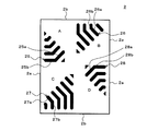
- FIG. FIG. 7 is a plan view showing the pixel electrode 2 in one pixel region of the display panel according to Embodiment 2 of the present invention.
- the pixel electrode 2 according to the present embodiment also has the liquid crystal molecule heads of the four liquid crystal domains A, B, C, and D of the pixel electrode 2 of the active matrix substrate 1.
- a group of slits 25, slits 26, slits 27, and slits 28 are formed on the side facing the.
- the slit 25 includes a tilt extension portion 25a extending in the tilt direction of the liquid crystal domain A and a linear portion 25b extending in a direction perpendicular to the outer side 2a of the pixel region.
- the angle formed by the straight line connecting the end portions of the tilt extension portions of each slit 25 and the outer side 2a is approximately 45 °, the straight line connecting the boundary portions between the respective tilt extension portions and the linear portions, and the outer side 2a
- the angle formed by is approximately 22.5 °.
- the slit 26 has a tilt extension portion 26a extending in the tilt direction of the liquid crystal domain B and a linear portion 26b extending in a direction perpendicular to the outer side 2b of the pixel region.
- the slit 27 has a tilt extension portion 27a extending in the tilt direction of the liquid crystal domain C and a linear portion 27b extending in a direction perpendicular to the outer side 2b of the pixel region. Some slits 27 do not have a linear portion 27b.
- the slit 28 has a tilt extension portion 28a extending in the tilt direction of the liquid crystal domain D and a linear portion 28b extending in a direction perpendicular to the outer side 2a of the pixel region.
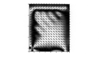
- FIG. 8 is a plan view showing a light transmission state in the pixel region of FIG. 7, and FIG. 9 is an enlarged view showing a portion of the liquid crystal domain B of FIG. FIG. 8 shows a state where wirings and contact holes are arranged, and in FIG. 9, the alignment of liquid crystal molecules is shown by pins.
- the liquid crystal molecules are aligned along the direction (tilt direction) in which the slits 26 extend, and as described above, the inner end portions are arranged in parallel to the direction crossing the tilt direction. Therefore, the alignment of the liquid crystal molecules is aligned without being disturbed.
- the slit 26 has the linear part 26b, the width
- the display panel 102 according to the present embodiment suppresses the generation of dark lines, and the slit has a linear portion. It can be seen that generation of dark lines is further suppressed as compared with the display panel 102 according to the first embodiment. From Table 1 above, it can be seen that the transmittance and the transmittance ratio are higher than those of the conventional display panel and the display panel 102 according to Embodiment 1.
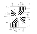
- FIG. 10 is a plan view showing the pixel electrode 2 in one pixel region of the display panel according to Embodiment 3 of the present invention.
- the pixel electrode 2 according to the present embodiment also includes liquid crystal molecules of four liquid crystal domains A, B, C, and D of the pixel electrode 2 of the active matrix substrate 1.
- a group of slits 41, slits 42, slits 43, and slits 44 are formed on the side facing the head.
- the slit 41 has a tilt extension portion 41a extending in the tilt direction of the liquid crystal domain A and a linear portion 41b extending in a direction perpendicular to the outer side 2a of the pixel region.
- the angle formed between the straight line connecting the ends of the tilt extension portions 41a of the slits 41 and the outer side 2a is approximately 45 °, the straight line connecting the boundary portions between the tilt extension portions 41a and the linear portions 41b, and the outer shape.
- the angle formed by the side 2a is approximately 22.5 °.
- the slit 42 includes a slit 421 having a tilt extension portion 42a extending in the tilt direction of the liquid crystal domain B, a linear portion 42b extending in a direction perpendicular to the outer side 2b of the pixel region, a slit 422 composed of a tilt extension portion, And a slit 423 made of a shaped portion.
- the slit 43 includes a slit 431 having a tilt extending portion 43a extending in the tilt direction of the liquid crystal domain C, a linear portion 43b extending in a direction perpendicular to the outer side 2b of the pixel region, a slit 432 including the tilt extending portion, And a slit 433 made of a shaped portion.
- the slit 44 has a tilt extension portion 44a extending in the tilt direction of the liquid crystal domain D and a linear portion 44b extending in a direction perpendicular to the outer side 2a of the pixel region, like the slit 41.
- the linear portion is not connected to the tilt extended portion and one of the tilt extended portion and the linear portion is included.
- the length of the linear portion can be controlled to 10 ⁇ m or more and 20 ⁇ m or less, and the dark line suppression effect can be maximized.
- FIG. 11 is a plan view showing a light transmission state in the pixel region of FIG. 10, and FIG. 12 is an enlarged view showing a portion of the liquid crystal domain B of FIG. FIG. 11 shows a state where wirings and contact holes are arranged, and in FIG. 12, the alignment of liquid crystal molecules is shown by pins.
- FIG. 12 shows that the generation of dark lines is further suppressed in the region where the slits 42 are formed. From Table 1 above, it can be seen that the transmittance and the transmittance ratio are higher than those of the conventional display panel and the display panel 102 according to the first and second embodiments.
- FIG. FIG. 13 is a plan view showing the pixel electrode 2 in one pixel region of the display panel according to Embodiment 4 of the present invention.
- the pixel electrode 2 according to the present embodiment also includes liquid crystal molecules of four liquid crystal domains A, B, C, and D of the pixel electrode 2 of the active matrix substrate 1.
- a group of slits 45, slits 46, slits 47, and slits 48 are formed on the side facing the head.
- the slit 45 has a tilt extending portion 45a extending in the tilt direction of the liquid crystal domain A and a linear portion 45b extending in a direction perpendicular to the outer side 2a of the pixel region, like the slit 41.
- the straight line connecting the inner end portions of the group of slits 45 is inclined counterclockwise by 5 ° with respect to the straight line connecting the inner end portions of the group of slits 41 according to the third embodiment.
- the angle formed is 50 °.
- the angle formed by the straight line connecting the boundary portions between the tilt extension portions 41a and the linear portions 41b and the outer side 2a is approximately 22.5 °.
- the slit 46 includes a slit extension 461 extending in the tilt direction of the liquid crystal domain B, a slit 461 having a linear part 46 b extending in a direction perpendicular to the outer side 2 b of the pixel region, a slit 462 including the tilt extension part, And a slit 463 formed of a shaped portion.
- the angle formed by the straight line connecting the inner ends of the group of slits 46 and the outer side 2a is 40 °.
- the slit 47 includes a slit 471 having a tilt extending portion 47a extending in the tilt direction of the liquid crystal domain C, a linear portion 47b extending in a direction perpendicular to the outer side 2b of the pixel region, a slit 472 including the tilt extending portion, And a slit 473 formed of a shaped portion.
- the angle formed by the straight line connecting the inner ends of the group of slits 47 and the outer side 2a is 40 °.
- the slit 48 has a tilt extension portion 48a extending in the tilt direction of the liquid crystal domain D and a linear portion 48b extending in a direction perpendicular to the lateral outline of the pixel region.
- the angle formed by the straight line connecting the inner ends of the group of slits 48 and the outer side 2a is 50 °.
- FIG. 14 is a plan view showing a light transmission state in the pixel region of FIG. FIG. 14 shows a state in which wiring and contact holes are arranged.
- FIG. 14 shows that the generation of dark lines is further suppressed, and from Table 1 above, the transmittance and the transmittance ratio are improved from those of the conventional display panel and the display panel 102 according to Embodiments 1 to 3. I understand that.
- FIG. FIG. 15 is a plan view showing the pixel electrode 2 in one pixel region of the display panel according to Embodiment 5 of the present invention.
- the pixel electrode 2 according to the present embodiment also includes liquid crystal molecules of the four liquid crystal domains A, B, C, and D of the pixel electrode 2 of the active matrix substrate 1.
- a group of slits 51, slits 52, slits 53, and slits 54 are formed on the side facing the head.
- the slit 51 is formed so that the inner end portion is aligned, similarly to the slit 21 of the display panel 102 according to Embodiment 1, but the angle formed by the straight line connecting the inner end portion and the outer side 2a of the pixel region. Is 50 °.
- the slits 52 are formed so that the inner end portions thereof are arranged in the same manner as the slits 22 of the display panel 102 according to the first embodiment, but the angle formed by the straight line connecting the inner end portions and the outer side 2a of the pixel region. Is 40 °.
- the slit 53 is formed so that the inner end portion is aligned like the slit 23 of the display panel 102 according to the first embodiment, but the angle formed by the straight line connecting the inner end portion and the outer side 2a of the pixel region. Is 40 °.
- the slits 54 are formed so that the inner end portions thereof are arranged in the same manner as the slit 24 of the display panel 102 according to the first embodiment, but the angle formed by the straight line connecting the inner end portions and the outer side 2a of the pixel region. Is 50 °.
- FIG. 16 is a plan view showing a light transmission state in the pixel region of FIG. FIG. 16 shows a state where wirings and contact holes are arranged. From FIG. 16, it can be seen that the generation of dark lines is suppressed as in FIG. 5. From Table 1, the transmittance and the transmittance ratio are the same as those of the display panel 102 according to the first embodiment. It can be seen that it is better than the panel.
- FIG. 17 is a plan view showing the pixel electrode 2 in one pixel region of the display panel according to Embodiment 6 of the present invention. In FIG. 17, contact holes and wirings are also shown. Similarly to the pixel electrode 2 according to the first to fifth embodiments, the pixel electrode 2 according to the present embodiment also includes liquid crystal molecules of four liquid crystal domains A, B, C, and D of the pixel electrode 2 of the active matrix substrate 1. A group of slits 55, slits 56, slits 57, and slits 58 are formed on the side facing the head.
- the slits 55, 56, 57, and 58 are also formed so that the inner end portions are aligned in the direction crossing each tilt direction. Yes.
- a slit extending in the tilt direction of each liquid crystal domain is also provided along the boundary of the liquid crystal domain.
- the display panel according to the present embodiment is formed such that the inner ends of the slits 55, 56, 57, and 58 are arranged in a direction crossing each tilt direction. Therefore, the generation of dark lines is suppressed well.
- the present invention is not limited to the contents of the first to sixth embodiments described above, and various modifications can be made within the scope of the claims. In other words, embodiments obtained by combining technical means appropriately modified within the scope of the claims are also included in the technical scope of the present invention.
- the angle formed by the straight line connecting one end of the slit and the outer side 2a may be in the range of 45 ° ⁇ 5 °.
- the tilt extension portion and the linear portion of the slit The angle formed by the straight line connecting the boundary portions and the outer side 2a may be in the range of 22.5 ⁇ 2.5 °.
- the shape of the slit is not limited to a rounded rectangular shape, and may be an elliptical shape or a rectangular shape.
Landscapes
- Physics & Mathematics (AREA)
- Nonlinear Science (AREA)
- Mathematical Physics (AREA)
- Chemical & Material Sciences (AREA)
- Crystallography & Structural Chemistry (AREA)
- General Physics & Mathematics (AREA)
- Optics & Photonics (AREA)
- Spectroscopy & Molecular Physics (AREA)
- Liquid Crystal (AREA)
Abstract
画素領域に光を透過した場合に生じる暗線の面積が小さく、光の透過率が良好であり、画質が良好である液晶表示装置を提供する。 液晶表示装置は、一面に電極及び光配向膜が順に形成され、一面同士が対向する2枚の基板と、垂直配向型の液晶材料を含み、両光配向膜間に介在する液晶層と、基板上に、該基板の面方向にマトリクス状に形成された複数の画素領域と、各画素領域に含まれ、両光配向膜により規定される基準配向方向が夫々異なる、少なくとも2つの液晶ドメインと、一方の電極の各液晶ドメインに対応する領域に形成され、各基準配向方向に平行に延びるスリット21、22、23、24とを有する。スリット21、22、23、24は、夫々の一端部が基準配向方向に交叉する方向に並ぶように形成されている。
Description
本発明は、テレビジョン受信機、パーソナルコンピュータ等に備えられる液晶表示装置に関する。
表示装置の中で、液晶表示装置は薄型であり、消費電力が低いという特徴を有する。 液晶表示装置の表示パネルは、カラーフィルタ(CF)基板と、液晶層と、アクティブマトリクス基板(TFT基板)と、2枚の偏光板とを有する。CF基板とアクティブマトリクス基板とはシール材を挟んで互いに貼り合わされており、その間に液晶が介在されて液晶層が形成されている。アクティブマトリクス基板は液晶層側に画素電極を有し、CF基板は液晶層側に共通電極を有する。2枚の偏光板は、CF基板及びアクティブマトリクス基板夫々の、液晶層側とは反対側の面上に配されている。
液晶材料として垂直配向型の材料を用いた液晶表示装置は、VA(Vertical Alignment)モードの液晶表示装置と呼ばれる。この液晶表示装置において透過率及び応答速度を向上させるために、1つの画素に複数の液晶ドメインを形成する配向分割構造が採用されている。この配向分割構造を形成する方法として、例えばMVA(Multi-domain Vertical Alignment )モードが挙げられる。MVAモードにおいては、液晶層を挟む基板の液晶層側に線状突起を設けたり、画素電極に開口部(スリット)を設けたりすることによって配向規制構造を得ており、この配向規制構造によって複数の液晶ドメインが形成されている(例えば特許文献1)。スリットを微細にすることにより、液晶分子の配向をより制御することができ、透過率及び応答速度の向上が図られている。
液晶層を挟んで対向する両基板の液晶層側に、プレチルト方向(配向処理方向)が互いに直交するように夫々、光配向膜等の配向膜を設け、電圧印加時に液晶分子がツイスト配向をとるように構成したVAモードはVATN(Vertical Alignment Twisted Nematic)モードと呼ばれる(例えば特許文献2)。このうち、一つの画素領域において、2つの配向膜でプレチルト方向を規定することにより、電圧印加時に、2行2列に分割された4つの液晶ドメインが形成される構造は4D構造と呼ばれる。
図18は、この4D構造を有するVATNモードの液晶表示装置の画素領域を示す平面図である。
図18中、点線矢印はアクティブマトリクス基板に設けられている光配向膜によって規定されるプレチルト方向を示し、実線矢印はCF基板に設けられている光配向膜によって規定されるプレチルト方向を示す。そして、液晶層に電圧を印加した場合の各液晶ドメインのチルト方向(基準配向方向)をピンの向きで示してある。ピンの円板部(頭部)が液晶表示装置を見る者に近くなるように、液晶分子がチルトしていることを示している。すなわち、基準配向方向は斜め45°である。
この液晶表示装置の画素電極にはスリットは形成されていない。
図18中、点線矢印はアクティブマトリクス基板に設けられている光配向膜によって規定されるプレチルト方向を示し、実線矢印はCF基板に設けられている光配向膜によって規定されるプレチルト方向を示す。そして、液晶層に電圧を印加した場合の各液晶ドメインのチルト方向(基準配向方向)をピンの向きで示してある。ピンの円板部(頭部)が液晶表示装置を見る者に近くなるように、液晶分子がチルトしていることを示している。すなわち、基準配向方向は斜め45°である。
この液晶表示装置の画素電極にはスリットは形成されていない。
図19は図18の画素領域の光透過状態を示す平面図、図20は図19の右上部分(液晶ドメインB部分)の拡大図である。図19及び図20においては、配線及びコンタクトホールが配された状態を示している。コンタクトホールは画素領域の中央部に形成されている。そして、図20においては、液晶分子の配向をピンで示してある。
図19及び図20より、画素領域の外形辺側及び液晶ドメインの境界において、広い幅を有する暗線が生じていることが分かる。画素領域の外形辺において、液晶分子は外形辺に対して垂直かつ内向きの方位に傾き、画素領域の外形辺の近傍では、外形辺で傾いた液晶分子と、チルト方向に配向した液晶分子との頭部が向き合っており、液晶分子の向きが乱れ、偏光軸に垂直又は平行な方向に液晶分子が曲げられて光が透過しない領域が生じる。液晶ドメインの境界においては、境界の両側でチルト角が90°異なるので、液晶分子が境界に垂直な方向(偏光軸に垂直又は平行な方向)に曲がって配向し、光が透過しない幅広の領域が生じる。
暗線により透過率が低下する。特に、画素が小さい高精細ディスプレイにおいては、暗線による透過率低下の影響が大きくなる。
図19及び図20より、画素領域の外形辺側及び液晶ドメインの境界において、広い幅を有する暗線が生じていることが分かる。画素領域の外形辺において、液晶分子は外形辺に対して垂直かつ内向きの方位に傾き、画素領域の外形辺の近傍では、外形辺で傾いた液晶分子と、チルト方向に配向した液晶分子との頭部が向き合っており、液晶分子の向きが乱れ、偏光軸に垂直又は平行な方向に液晶分子が曲げられて光が透過しない領域が生じる。液晶ドメインの境界においては、境界の両側でチルト角が90°異なるので、液晶分子が境界に垂直な方向(偏光軸に垂直又は平行な方向)に曲がって配向し、光が透過しない幅広の領域が生じる。
暗線により透過率が低下する。特に、画素が小さい高精細ディスプレイにおいては、暗線による透過率低下の影響が大きくなる。
4D構造を有するVATNモードに、上述のMVAモードを組み合わせることも行なわれている(例えば特許文献3等)。
図21は、特許文献3の液晶表示装置の画素領域におけるアクティブマトリクス基板の画素電極を示す平面図である。
画素電極の各液晶ドメインには、画素領域の外形辺に沿って、該外形辺に垂直な方向に延びる複数のスリットが並設されている。
この液晶表示装置においては、画素領域の外形辺側に生じていた暗線に対応して前記スリット群を設けることにより液晶分子の配向を制御し、透過率を上げることを図っている。
図21は、特許文献3の液晶表示装置の画素領域におけるアクティブマトリクス基板の画素電極を示す平面図である。
画素電極の各液晶ドメインには、画素領域の外形辺に沿って、該外形辺に垂直な方向に延びる複数のスリットが並設されている。
この液晶表示装置においては、画素領域の外形辺側に生じていた暗線に対応して前記スリット群を設けることにより液晶分子の配向を制御し、透過率を上げることを図っている。
図22は図21の画素領域に配線及びコンタクトホールが配された場合の光透過状態を示す平面図、図23は図22の液晶ドメインBの部分の拡大図である。
図22より、楕円で囲んだ、スリット群の内側の端部において暗線が生じていることが分かる。
これは、図23に示すように、スリットの切れ目の部分で液晶分子の配向が乱れ、液晶分子が衝突してスリットの端部が並ぶ方向に、即ち、偏光軸に垂直又は平行な方向に曲げられ、光が透過できない領域が生じるためである。
特に、高精細の液晶表示装置の場合、画素領域の大きさが小さいので、スリットが切れる部分における液晶分子の配向の乱れによる影響が大きく、透過率の低下量が大きくなる。
図22より、楕円で囲んだ、スリット群の内側の端部において暗線が生じていることが分かる。
これは、図23に示すように、スリットの切れ目の部分で液晶分子の配向が乱れ、液晶分子が衝突してスリットの端部が並ぶ方向に、即ち、偏光軸に垂直又は平行な方向に曲げられ、光が透過できない領域が生じるためである。
特に、高精細の液晶表示装置の場合、画素領域の大きさが小さいので、スリットが切れる部分における液晶分子の配向の乱れによる影響が大きく、透過率の低下量が大きくなる。
本発明は斯かる事情に鑑みてなされたものであり、画素領域に光を透過した場合に生じる暗線の面積が小さく、光の透過率が良好であり、画質が良好である液晶表示装置を提供することを目的とする。
本発明に係る液晶表示装置は、一面に電極及び光配向膜が順に形成され、一面同士が対向する2枚の基板と、垂直配向型の液晶材料を含み、両光配向膜間に介在する液晶層と、前記基板上に、該基板の面方向にマトリクス状に形成された複数の画素領域と、各画素領域に含まれ、両光配向膜により規定される基準配向方向が夫々異なる、少なくとも2つの液晶ドメインと、一方の電極の各液晶ドメインに対応する領域に形成され、各基準配向方向に平行に延びる複数の開口部とを有する液晶表示装置において、各液晶ドメインにおける各開口部は、各開口部の一端部が前記基準配向方向に交叉する方向に並ぶように形成されていることを特徴とする。
本発明においては、液晶分子は、開口部が延びる方向(基準配向方向)に沿って配向し、一端部が基準配向方向に交叉する方向に並ぶように設けられているので、該一端部において液晶分子の配向が乱れない。液晶分子は開口部の切れ目で複数の方向に向くので、開口部間で端部が揃っていない場合、隣り合う開口部の液晶分子が端部側で干渉し、曲げられて偏光軸に垂直又は平行な方向に配向し、暗線が生じる。本実施の形態においては、端部側で隣り合う液晶分子が干渉するのが抑制されている。
従って、本発明に係る液晶表示装置においては、画素領域に光を透過した場合に生じる暗線の面積が小さく、光の透過率が良好であり、画質が良好である。
図21の従来の液晶表示装置のように、開口部が偏光軸に垂直又は平行な方向に並設されている場合、図23に示すように、開口部の端部が並んでいても、液晶分子は基準配向方向に配向しているので、端部側で隣り合う開口部の液晶分子が干渉することになり、向きが偏光軸に垂直又は平行な方向に曲げられる。
従って、本発明に係る液晶表示装置においては、画素領域に光を透過した場合に生じる暗線の面積が小さく、光の透過率が良好であり、画質が良好である。
図21の従来の液晶表示装置のように、開口部が偏光軸に垂直又は平行な方向に並設されている場合、図23に示すように、開口部の端部が並んでいても、液晶分子は基準配向方向に配向しているので、端部側で隣り合う開口部の液晶分子が干渉することになり、向きが偏光軸に垂直又は平行な方向に曲げられる。
本発明に係る液晶表示装置は、各開口部の他端部も直線上に並ぶように形成されていることを特徴とする。
本発明においては、開口部の他端部も直線上に並ぶように形成されているので、液晶分子の配向が乱れず、暗線の発生がより抑制される。
本発明に係る液晶表示装置は、前記開口部は、前記画素領域の外形辺に垂直な方向に延びる線状部分を有することを特徴とする。
本発明においては、線状部分を有するので、外形辺側に生じる暗線の幅が狭くなる。これは、線状部分の端部と、前記外形辺との隙間に存在する液晶分子が、端部及び外形辺に沿って並ぶ液晶分子により押されて曲げられ、外形辺に平行な方向に、幅の狭い領域内で並ぶためであると考えられる。
本発明に係る液晶表示装置は、前記線状部分の長さが10μm以上、20μm未満であることを特徴とする。
本発明においては、暗線がより良好に抑制される。
本発明に係る液晶表示装置は、各開口部の一端部を繋ぐ直線と、前記外形辺とがなす角度は略45度であり、各開口部の基準配向方向に平行に延びる部分と、前記線状部分との境界部分を繋ぐ直線と、前記外形辺とがなす角度は略22.5度であることを特徴とする。
本発明においては、線状部分を、幅が変わることなく、基準配向方向に平行に延びる部分に良好に連設することができる。
本発明に係る液晶表示装置は、前記2枚の基板を光が透過するように構成されており、前記開口部は、前記液晶層の厚み方向の中央部における液晶分子の光出射側の端部向く側に設けられていることを特徴とする。
本発明においては、開口部がない場合に暗線が生じる部分に集中的に開口部を設けるので、暗線の発生が良好に抑制される。
そして、開口部が設けられている部分が限定されているので、液晶表示装置がタッチパネルとして構成されている場合に、指の押圧による液晶分子の配向の乱れからの復帰が早くなり、ムラが抑制されている。
そして、開口部が設けられている部分が限定されているので、液晶表示装置がタッチパネルとして構成されている場合に、指の押圧による液晶分子の配向の乱れからの復帰が早くなり、ムラが抑制されている。
本発明によれば、各基準配向方向に平行に延びる各開口部は、一端部が各基準配向方向に交叉する方向に並ぶように形成されているので、端部において、液晶分子の配向(各基準配向方向に平行な向き)が乱れず、暗線の発生が抑制されている。
従って、本発明に係る液晶表示装置においては、画素領域に光を透過した場合に生じる暗線の面積が小さく、光の透過率が良好であり、画質が良好である。
従って、本発明に係る液晶表示装置においては、画素領域に光を透過した場合に生じる暗線の面積が小さく、光の透過率が良好であり、画質が良好である。
以下、本発明をその実施の形態を示す図面に基づいて具体的に説明する。
実施の形態1.
図1は本発明の実施の形態1に係る液晶表示装置100の外観斜視図、図2は液晶表示装置100の表示パネル102の一画素領域における画素電極2を示す平面図、図3は図2のIII -III 線における表示モジュール101の断面図、図4はアクティブマトリクス基板1の配線を示す平面図である。
実施の形態1.
図1は本発明の実施の形態1に係る液晶表示装置100の外観斜視図、図2は液晶表示装置100の表示パネル102の一画素領域における画素電極2を示す平面図、図3は図2のIII -III 線における表示モジュール101の断面図、図4はアクティブマトリクス基板1の配線を示す平面図である。
液晶表示装置100は、表示パネル102及びバックライトユニット103を有する表示モジュール101と、該表示モジュール101を挟むようにして収容する合成樹脂製のフロントキャビネット104及びリアキャビネット105と、スタンド106とを備える。表示モジュール101は、全体として横長の略直方体状をなし、縦姿勢でフロントキャビネット104及びリアキャビネット105内に収容されている。
実施の形態1に係る表示パネル102は、面方向にマトリクス状に配された複数の画素領域を有する。
表示パネル102はマルチドメインのVATNモードの表示パネルであり、図2に示すように、アクティブマトリクス基板1の画素電極2の4つの液晶ドメインA、B、C、Dには、角丸長方形状をなし、各液晶ドメインの斜め45°のチルト方向に対応して延びる一群のスリット21、スリット22、スリット23、及びスリット24が形成されている。
表示パネル102はマルチドメインのVATNモードの表示パネルであり、図2に示すように、アクティブマトリクス基板1の画素電極2の4つの液晶ドメインA、B、C、Dには、角丸長方形状をなし、各液晶ドメインの斜め45°のチルト方向に対応して延びる一群のスリット21、スリット22、スリット23、及びスリット24が形成されている。
スリット21は、液晶ドメインAのうちの、図18における液晶分子の頭部が向く側(液晶層6の厚み方向の中央部における液晶分子のCF基板7側の端部が向く側)に、即ち、液晶ドメインAのチルト方向に交叉する方向の対角線より下側に設けられている。
そして、各スリット21は、各スリット21の内側端部が前記チルト方向に交叉する方向に並ぶように形成されている。即ち、内側端部を繋ぐ直線は画素領域の縦の外形辺2aに対し略45°の角度をなしている。各スリット21の、画素領域の縦の外形辺2a及び横の外形辺2bに平行である方の各端部も並ぶように形成されている。チルト方向に交叉する方向の両端側のスリット21は三角形状をなす。
そして、各スリット21は、各スリット21の内側端部が前記チルト方向に交叉する方向に並ぶように形成されている。即ち、内側端部を繋ぐ直線は画素領域の縦の外形辺2aに対し略45°の角度をなしている。各スリット21の、画素領域の縦の外形辺2a及び横の外形辺2bに平行である方の各端部も並ぶように形成されている。チルト方向に交叉する方向の両端側のスリット21は三角形状をなす。
スリット22、23、24もスリット21と同様に、液晶ドメインB、C、Dの、図18における液晶分子の頭部が向く側に設けられている。そして、スリット22、23、24は、スリット22、23、24の内側の端部が各チルト方向に交叉する方向に並ぶように形成され、各スリット22、23、24の、画素領域の外形辺2a及び外形辺2bに平行である方の各端部も並ぶように形成されている。各スリットの内側端部を繋ぐ直線は画素領域の外形辺2aに対し略45°の角度をなしている。
画素電極2は例えばスパッタリング法によりITO膜を形成した後、パターニングすることにより、スリット21、22、23、及び24を有した状態で形成される。画素領域の中央部にはコンタクトホール(不図示)が形成されており、コンタクトホール上にも画素電極2が形成されている。
図3に示すように、表示モジュール101の表示パネル102は、アクティブマトリクス基板1と、CF基板7と、液晶層6と、2枚の偏光板4,11とを有する。CF基板7とアクティブマトリクス基板1とはシール材を挟んで互いに貼り合わされており、その間に垂直配向型の液晶材料が注入され、液晶層6が形成されている。2枚の偏光板11,4は、CF基板7,アクティブマトリクス基板1夫々の、液晶層6側とは反対側の面上に配されている。
アクティブマトリクス基板1の基板部3は、例えばガラス製の絶縁性基板に、後述するTFT(薄膜トランジスタ)36(図4参照)と、TFT36に走査信号を与える、複数のゲート配線(走査配線)31と、TFT36に映像信号を与える複数のソース配線(信号配線)33とを形成してなる。
図4に示すように、ゲート配線31及びCs配線32は互いに平行に延び、ソース配線33は、ゲート配線31及びCs配線32に交叉し、かつ互いに平行に延びている。
Cs配線32は、中央部に、矩形状をなすドレイン対向部321を有する。
図4における左側のソース配線33の下端部には、右側のソース配線33に向かうように、矩形状をなすソース電極331が設けられている。
Cs配線32は、中央部に、矩形状をなすドレイン対向部321を有する。
図4における左側のソース配線33の下端部には、右側のソース配線33に向かうように、矩形状をなすソース電極331が設けられている。
ドレイン電極35は、ドレイン対向部321より少し小さい矩形状をなすCs対向部351と、ソース電極331と面方向で対向するソース電極対向部352とを有する。 Cs配線32のドレイン対向部321と、ドレイン電極35のCs対向部351とは、ゲート絶縁膜(不図示)が介在する状態で対向しており、この領域で補助容量(Cs)が形成される。
下側のゲート配線31の左寄りの部分にはゲート電極が形成され、該ゲート電極、ソース電極331、及びソース電極対向部352によりTFT36が構成される。
下側のゲート配線31の左寄りの部分にはゲート電極が形成され、該ゲート電極、ソース電極331、及びソース電極対向部352によりTFT36が構成される。
基板部3の液晶層6側に上述のスリット21、22、23、及び24を有する画素電極2が形成されており、画素電極2は光配向膜5に覆われている。コンタクトホールを介して、ドレイン電極35は画素電極2に電気的に接続されている。
CF基板7の基板部10は、例えばガラス製の絶縁性基板に、ブラックマトリックス(BM)、並びにR(赤)、G(緑)、及びB(青)等のカラーフィルタ(不図示)を配列してなる。
基板部10の液晶層6側には、例えばITO等からなる共通電極9が形成されている。共通電極9は光配向膜8により覆われている。
偏光板4及び11は、夫々偏光軸が互いに直交するように配置されている。
基板部10の液晶層6側には、例えばITO等からなる共通電極9が形成されている。共通電極9は光配向膜8により覆われている。
偏光板4及び11は、夫々偏光軸が互いに直交するように配置されている。
バックライトユニット103は、表示パネル102の背面側に配される。バックライトユニット103は、エッジライト方式(サイドライト方式、導光板方式)、及び直下型方式のいずれであってもよい。エッジライト方式の場合、バックライトユニット103は、光学シート、導光板、及びLED基板等の光源をシャーシに収納してなる。
図5は、上述の図2の画素領域における光透過状態を示す平面図、図6は図5の右上部分(液晶ドメインBの部分)を示す拡大図である。図5においては、配線及びコンタクトホールが配された状態を示しており、図6においては、液晶分子の配向をピンで示してある。
本実施の形態においては、液晶ドメイン境界に生じる暗線の領域上にアクティブマトリクス基板1のメタル配線(Cs配線32、ゲート配線31、ドレイン電極35)が位置するようにして、光の透過ロスを抑制している。
本実施の形態においては、液晶ドメイン境界に生じる暗線の領域上にアクティブマトリクス基板1のメタル配線(Cs配線32、ゲート配線31、ドレイン電極35)が位置するようにして、光の透過ロスを抑制している。
図6に示すように、液晶分子は、スリット22が延びる方向(チルト方向)に沿って配向しており、上述したように内側の端部がチルト方向に交叉する方向に並ぶように設けられているので、内側端部において液晶分子の配向が乱れず、揃っている。液晶分子はスリットの切れ目で複数の方向に向くので、スリット間で端部が揃っていない場合、隣り合うスリットの液晶分子が端部側で干渉し、曲げられて偏光軸に垂直又は平行な方向に配向し、暗線が生じると考えられる。
図5及び図6を、従来の表示パネルの画素領域における光透過状態を示した図19及び図22と比較することにより、本実施の形態に係る表示パネル102においては暗線の発生が良好に抑制されていることが分かる。
下記の表1に、本実施の形態に係る表示パネル102、上述の従来の図19及び図22の表示パネルの透過率を示す。併せて、図19の表示パネルの透過率を1.00とした場合の各表示パネルの透過率の比率(透過率比)も示す。
下記の表1に、本実施の形態に係る表示パネル102、上述の従来の図19及び図22の表示パネルの透過率を示す。併せて、図19の表示パネルの透過率を1.00とした場合の各表示パネルの透過率の比率(透過率比)も示す。

表1より、本実施の形態の表示パネル102は従来の表示パネルと比較して透過率が向上していることが分かる。
従って、表示パネル102を備える液晶表示装置100の画質は良好である。
そして、本実施の形態においては、スリット22が設けられている部分が限定されているので、液晶表示装置100がタッチパネルとして構成されている場合に、指の押圧による液晶分子の配向の乱れからの復帰が早くなり、ムラが抑制されている。
従って、表示パネル102を備える液晶表示装置100の画質は良好である。
そして、本実施の形態においては、スリット22が設けられている部分が限定されているので、液晶表示装置100がタッチパネルとして構成されている場合に、指の押圧による液晶分子の配向の乱れからの復帰が早くなり、ムラが抑制されている。
実施の形態2.
図7は、本発明の実施の形態2に係る表示パネルの一画素領域における画素電極2を示す平面図である。
本実施の形態に係る画素電極2も、実施の形態1に係る画素電極2と同様に、アクティブマトリクス基板1の画素電極2の4つの液晶ドメインA、B、C、Dの液晶分子の頭部が向く側に、一群のスリット25、スリット26、スリット27、及びスリット28が形成されている。
図7は、本発明の実施の形態2に係る表示パネルの一画素領域における画素電極2を示す平面図である。
本実施の形態に係る画素電極2も、実施の形態1に係る画素電極2と同様に、アクティブマトリクス基板1の画素電極2の4つの液晶ドメインA、B、C、Dの液晶分子の頭部が向く側に、一群のスリット25、スリット26、スリット27、及びスリット28が形成されている。
スリット25は、液晶ドメインAのチルト方向に延びるチルト伸長部分25aと、画素領域の外形辺2aに垂直な方向に延びる線状部分25bとを有する。各スリット25のチルト伸長部分の端部を繋ぐ直線と、外形辺2aとがなす角度は略45°であり、各チルト伸長部分と線状部分との境界部分を繋ぐ直線と、外形辺2aとがなす角度は略22.5°である。
スリット26も同様に、液晶ドメインBのチルト方向に延びるチルト伸長部分26aと、画素領域の外形辺2bに垂直な方向に延びる線状部分26bとを有する。スリット26の中には線状部分26bを有さないものもある。
スリット27も同様に、液晶ドメインCのチルト方向に延びるチルト伸長部分27aと、画素領域の外形辺2bに垂直な方向に延びる線状部分27bとを有する。スリット27の中には線状部分27bを有さないものもある。
スリット28も同様に、液晶ドメインDのチルト方向に延びるチルト伸長部分28aと、画素領域の外形辺2aに垂直な方向に延びる線状部分28bとを有する。
スリット26も同様に、液晶ドメインBのチルト方向に延びるチルト伸長部分26aと、画素領域の外形辺2bに垂直な方向に延びる線状部分26bとを有する。スリット26の中には線状部分26bを有さないものもある。
スリット27も同様に、液晶ドメインCのチルト方向に延びるチルト伸長部分27aと、画素領域の外形辺2bに垂直な方向に延びる線状部分27bとを有する。スリット27の中には線状部分27bを有さないものもある。
スリット28も同様に、液晶ドメインDのチルト方向に延びるチルト伸長部分28aと、画素領域の外形辺2aに垂直な方向に延びる線状部分28bとを有する。
図8は図7の画素領域における光透過状態を示す平面図、図9は図8の液晶ドメインBの部分を示す拡大図である。図8においては、配線及びコンタクトホールが配された状態を示しており、図9においては、液晶分子の配向をピンで示してある。
図9に示すように、液晶分子は、スリット26が延びる方向(チルト方向)に沿って配向し、上述したように内側の端部がチルト方向に交叉する方向に平行に並ぶように設けられているので、液晶分子の配向が乱れることなく、揃っている。
さらに、スリット26は線状部分26bを有するので、外形辺2b側に生じる暗線の幅が狭くなっている。これは、線状部分26bの端部と、外形辺2bとの隙間に存在する液晶分子が、端部及び外形辺2bに沿って並ぶ液晶分子により押されて曲げられ、横方向に幅の狭い領域内で並ぶためであると考えられる。
図9に示すように、液晶分子は、スリット26が延びる方向(チルト方向)に沿って配向し、上述したように内側の端部がチルト方向に交叉する方向に平行に並ぶように設けられているので、液晶分子の配向が乱れることなく、揃っている。
さらに、スリット26は線状部分26bを有するので、外形辺2b側に生じる暗線の幅が狭くなっている。これは、線状部分26bの端部と、外形辺2bとの隙間に存在する液晶分子が、端部及び外形辺2bに沿って並ぶ液晶分子により押されて曲げられ、横方向に幅の狭い領域内で並ぶためであると考えられる。
図8及び図9を、図19及び図22と比較することにより、本実施の形態に係る表示パネル102においては、暗線の発生が抑制されており、スリットが線状部分を有することで、実施の形態1に係る表示パネル102と比較して暗線の発生がより抑制されていることが分かる。
そして、上記表1より透過率、及び透過率比が、従来の表示パネル、及び実施の形態1に係る表示パネル102より向上していることが分かる。
そして、上記表1より透過率、及び透過率比が、従来の表示パネル、及び実施の形態1に係る表示パネル102より向上していることが分かる。
実施の形態3.
図10は、本発明の実施の形態3に係る表示パネルの一画素領域における画素電極2を示す平面図である。
本実施の形態に係る画素電極2も、実施の形態1及び2に係る画素電極2と同様に、アクティブマトリクス基板1の画素電極2の4つの液晶ドメインA、B、C、Dの液晶分子の頭部が向く側に、一群のスリット41、スリット42、スリット43、及びスリット44が形成されている。
図10は、本発明の実施の形態3に係る表示パネルの一画素領域における画素電極2を示す平面図である。
本実施の形態に係る画素電極2も、実施の形態1及び2に係る画素電極2と同様に、アクティブマトリクス基板1の画素電極2の4つの液晶ドメインA、B、C、Dの液晶分子の頭部が向く側に、一群のスリット41、スリット42、スリット43、及びスリット44が形成されている。
スリット41は、スリット25と同様に、液晶ドメインAのチルト方向に延びるチルト伸長部分41aと、画素領域の外形辺2aに垂直な方向に延びる線状部分41bとを有する。各スリット41のチルト伸長部分41aの端部を繋ぐ直線と、外形辺2aとがなす角度は略45°であり、各チルト伸長部分41aと線状部分41bとの境界部分を繋ぐ直線と、外形辺2aとがなす角度は略22.5°である。
スリット42は、液晶ドメインBのチルト方向に延びるチルト伸長部分42a、及び画素領域の外形辺2bに垂直な方向に延びる線状部分42bを有するスリット421と、チルト伸長部分からなるスリット422と、線状部分からなるスリット423とを含む。
スリット43は、液晶ドメインCのチルト方向に延びるチルト伸長部分43a、及び画素領域の外形辺2bに垂直な方向に延びる線状部分43bを有するスリット431と、チルト伸長部分からなるスリット432と、線状部分からなるスリット433とを備える。
スリット44はスリット41と同様に、液晶ドメインDのチルト方向に延びるチルト伸長部分44aと、画素領域の外形辺2aに垂直な方向に延びる線状部分44bとを有する。
本実施の形態においては、チルト伸長部分に線状部分が連設されずに、チルト伸長部分及び線状部分の一方を有する場合を含んでいる。
このように連結しない部分を作ることによって、線状部分の長さを10μm以上、20μm以下に制御することが可能となり、暗線の抑制効果を最大限に上げる事ができる。
このように連結しない部分を作ることによって、線状部分の長さを10μm以上、20μm以下に制御することが可能となり、暗線の抑制効果を最大限に上げる事ができる。
図11は図10の画素領域における光透過状態を示す平面図、図12は図11の液晶ドメインBの部分を示す拡大図である。図11においては、配線及びコンタクトホールが配された状態を示しており、図12においては、液晶分子の配向をピンで示してある。
図12より、スリット42が形成されている領域において、暗線の発生がさらに抑制されていることが分かる。
そして、上記表1より透過率、及び透過率比が、従来の表示パネル、及び実施の形態1及び2に係る表示パネル102より向上していることが分かる。
そして、上記表1より透過率、及び透過率比が、従来の表示パネル、及び実施の形態1及び2に係る表示パネル102より向上していることが分かる。
実施の形態4.
図13は、本発明の実施の形態4に係る表示パネルの一画素領域における画素電極2を示す平面図である。
本実施の形態に係る画素電極2も、実施の形態1~3に係る画素電極2と同様に、アクティブマトリクス基板1の画素電極2の4つの液晶ドメインA、B、C、Dの液晶分子の頭部が向く側に、一群のスリット45、スリット46、スリット47、及びスリット48が形成されている。
図13は、本発明の実施の形態4に係る表示パネルの一画素領域における画素電極2を示す平面図である。
本実施の形態に係る画素電極2も、実施の形態1~3に係る画素電極2と同様に、アクティブマトリクス基板1の画素電極2の4つの液晶ドメインA、B、C、Dの液晶分子の頭部が向く側に、一群のスリット45、スリット46、スリット47、及びスリット48が形成されている。
スリット45は、スリット41と同様に、液晶ドメインAのチルト方向に延びるチルト伸長部分45aと、画素領域の外形辺2aに垂直な方向に延びる線状部分45bとを有する。一群のスリット45の内側端部を繋ぐ直線は、実施の形態3に係る一群のスリット41の内側端部を繋ぐ直線に対して5°、反時計回りに傾いており、即ち、外形辺2aとなす角度が50°である。各チルト伸長部分41aと線状部分41bとの境界部分を繋ぐ直線と、外形辺2aとがなす角度は略22.5°である。
スリット46は、液晶ドメインBのチルト方向に延びるチルト伸長部分46a、及び画素領域の外形辺2bに垂直な方向に延びる線状部分46bを有するスリット461と、チルト伸長部分からなるスリット462と、線状部分からなるスリット463とを備える。一群のスリット46の内側端部を繋ぐ直線と外形辺2aとがなす角度は40°である。
スリット47は、液晶ドメインCのチルト方向に延びるチルト伸長部分47a、及び画素領域の外形辺2bに垂直な方向に延びる線状部分47bを有するスリット471と、チルト伸長部分からなるスリット472と、線状部分からなるスリット473とを備える。一群のスリット47の内側端部を繋ぐ直線と外形辺2aとがなす角度は40°である。
スリット48はスリット45と同様に、液晶ドメインDのチルト方向に延びるチルト伸長部分48aと、画素領域の横の外形辺に垂直な方向に延びる線状部分48bとを有する。一群のスリット48の内側端部を繋ぐ直線と外形辺2aとがなす角度は50°である。
図14は図13の画素領域における光透過状態を示す平面図である。図14においては、配線及びコンタクトホールが配された状態を示している。
図14より暗線の発生がさらに抑制されていることが分かり、上記表1より透過率、及び透過率比が、従来の表示パネル、及び実施の形態1~3に係る表示パネル102より向上していることが分かる。
図14より暗線の発生がさらに抑制されていることが分かり、上記表1より透過率、及び透過率比が、従来の表示パネル、及び実施の形態1~3に係る表示パネル102より向上していることが分かる。
実施の形態5.
図15は、本発明の実施の形態5に係る表示パネルの一画素領域における画素電極2を示す平面図である。
本実施の形態に係る画素電極2も、実施の形態1~4に係る画素電極2と同様に、アクティブマトリクス基板1の画素電極2の4つの液晶ドメインA、B、C、Dの液晶分子の頭部が向く側に、一群のスリット51、スリット52、スリット53、及びスリット54が形成されている。
図15は、本発明の実施の形態5に係る表示パネルの一画素領域における画素電極2を示す平面図である。
本実施の形態に係る画素電極2も、実施の形態1~4に係る画素電極2と同様に、アクティブマトリクス基板1の画素電極2の4つの液晶ドメインA、B、C、Dの液晶分子の頭部が向く側に、一群のスリット51、スリット52、スリット53、及びスリット54が形成されている。
スリット51は、実施の形態1に係る表示パネル102のスリット21と同様に、内側端部が並ぶように形成されているが、内側端部を繋ぐ直線と画素領域の外形辺2aとがなす角度は50°である。
スリット52は、実施の形態1に係る表示パネル102のスリット22と同様に、内側端部が並ぶように形成されているが、内側端部を繋ぐ直線と画素領域の外形辺2aとがなす角度は40°である。
スリット53は、実施の形態1に係る表示パネル102のスリット23と同様に、内側端部が並ぶように形成されているが、内側端部を繋ぐ直線と画素領域の外形辺2aとがなす角度は40°である。
スリット54は、実施の形態1に係る表示パネル102のスリット24と同様に、内側端部が並ぶように形成されているが、内側端部を繋ぐ直線と画素領域の外形辺2aとがなす角度は50°である。
スリット52は、実施の形態1に係る表示パネル102のスリット22と同様に、内側端部が並ぶように形成されているが、内側端部を繋ぐ直線と画素領域の外形辺2aとがなす角度は40°である。
スリット53は、実施の形態1に係る表示パネル102のスリット23と同様に、内側端部が並ぶように形成されているが、内側端部を繋ぐ直線と画素領域の外形辺2aとがなす角度は40°である。
スリット54は、実施の形態1に係る表示パネル102のスリット24と同様に、内側端部が並ぶように形成されているが、内側端部を繋ぐ直線と画素領域の外形辺2aとがなす角度は50°である。
図16は図15の画素領域における光透過状態を示す平面図である。図16においては、配線及びコンタクトホールが配された状態を示している。
図16より図5と同様に暗線の発生が抑制されていることが分かり、上記表1より透過率、及び透過率比が、実施の形態1に係る表示パネル102と同等であり、従来の表示パネルより向上していることが分かる。
図16より図5と同様に暗線の発生が抑制されていることが分かり、上記表1より透過率、及び透過率比が、実施の形態1に係る表示パネル102と同等であり、従来の表示パネルより向上していることが分かる。
実施の形態6.
図17は、本発明の実施の形態6に係る表示パネルの一画素領域における画素電極2を示す平面図である。図17においては、コンタクトホール及び配線も示してある。
本実施の形態に係る画素電極2も、実施の形態1~5に係る画素電極2と同様に、アクティブマトリクス基板1の画素電極2の4つの液晶ドメインA、B、C、Dの液晶分子の頭部が向く側に、一群のスリット55、スリット56、スリット57、及びスリット58が形成されている。
図17は、本発明の実施の形態6に係る表示パネルの一画素領域における画素電極2を示す平面図である。図17においては、コンタクトホール及び配線も示してある。
本実施の形態に係る画素電極2も、実施の形態1~5に係る画素電極2と同様に、アクティブマトリクス基板1の画素電極2の4つの液晶ドメインA、B、C、Dの液晶分子の頭部が向く側に、一群のスリット55、スリット56、スリット57、及びスリット58が形成されている。
スリット55、56、57、58も実施の形態1に係る表示パネル102のスリット21、22、23、24と同様に、内側の端部が各チルト方向に交叉する方向に並ぶように形成されている。
本実施の形態においては、さらに液晶ドメインの境界に沿って、各液晶ドメインのチルト方向に延びるスリットも設けられている。
本実施の形態においては、さらに液晶ドメインの境界に沿って、各液晶ドメインのチルト方向に延びるスリットも設けられている。
本実施の形態に係る表示パネルも実施の形態1~5に係る表示パネルと同様に、スリット55、56、57、58の内側の端部が各チルト方向に交叉する方向に並ぶように形成されているので、暗線の発生が良好に抑制されている。
なお、本発明は上述した実施の形態1~6の内容に限定されるものではなく、請求項に示した範囲で種々の変更が可能である。すなわち、請求項に示した範囲で適宜変更した技術的手段を組み合わせて得られる実施形態も本発明の技術的範囲に含まれる。
例えば、スリットの一端部を繋ぐ直線と、外形辺2aとがなす角度は45°±5°の範囲であればよく、スリットが線状部分を有する場合、スリットのチルト伸長部分と線状部分との境界部分を繋ぐ直線と、外形辺2aとがなす角度は22.5±2.5°の範囲であればよい。
スリットの形状も角丸長方形状である場合に限定されるものではなく、楕円状でもよく、長方形状でもよい。
例えば、スリットの一端部を繋ぐ直線と、外形辺2aとがなす角度は45°±5°の範囲であればよく、スリットが線状部分を有する場合、スリットのチルト伸長部分と線状部分との境界部分を繋ぐ直線と、外形辺2aとがなす角度は22.5±2.5°の範囲であればよい。
スリットの形状も角丸長方形状である場合に限定されるものではなく、楕円状でもよく、長方形状でもよい。
1 アクティブマトリクス基板
2 画素電極
21、22、23、24、25、26、27、28、41、42、43、44、45、46、47、48、51、52、53、54 スリット
25a、26a、27a、28a、41a、42a、43a、44a、45a、46a、47a、48a チルト伸長部分
25b、26b、27b、28b、41b、42b、43b、44b、45b、46b、47b、48b チルト伸長部分
3、10 基板部
31 ゲート配線
32 Cs配線
33 ソース配線
35 ドレイン電極
36 TFT
4、11 偏光板
5、8 光配向膜
6 液晶層
61 液晶分子
7 CF基板
9 共通電極
12 コンタクトホール
100 液晶表示装置
101 表示モジュール
102 表示パネル
103 バックライトユニット
2 画素電極
21、22、23、24、25、26、27、28、41、42、43、44、45、46、47、48、51、52、53、54 スリット
25a、26a、27a、28a、41a、42a、43a、44a、45a、46a、47a、48a チルト伸長部分
25b、26b、27b、28b、41b、42b、43b、44b、45b、46b、47b、48b チルト伸長部分
3、10 基板部
31 ゲート配線
32 Cs配線
33 ソース配線
35 ドレイン電極
36 TFT
4、11 偏光板
5、8 光配向膜
6 液晶層
61 液晶分子
7 CF基板
9 共通電極
12 コンタクトホール
100 液晶表示装置
101 表示モジュール
102 表示パネル
103 バックライトユニット
Claims (6)
- 一面に電極及び光配向膜が順に形成され、一面同士が対向する2枚の基板と、
垂直配向型の液晶材料を含み、両光配向膜間に介在する液晶層と、
前記基板上に、該基板の面方向にマトリクス状に形成された複数の画素領域と、
各画素領域に含まれ、両光配向膜により規定される基準配向方向が夫々異なる、少なくとも2つの液晶ドメインと、
一方の電極の各液晶ドメインに対応する領域に形成され、各基準配向方向に平行に延びる複数の開口部と
を有する液晶表示装置において、
各液晶ドメインにおける各開口部は、各開口部の一端部が前記基準配向方向に交叉する方向に並ぶように形成されていることを特徴とする液晶表示装置。 - 各開口部の他端部も直線上に並ぶように形成されていることを特徴とする請求項1に記載の液晶表示装置。
- 前記開口部は、前記画素領域の外形辺に垂直な方向に延びる線状部分を有することを特徴とする請求項2に記載の液晶表示装置。
- 前記線状部分の長さは、10μm以上、20μm未満であることを特徴とする請求項3に記載の液晶表示装置。
- 各開口部の一端部を繋ぐ直線と、前記外形辺とがなす角度は略45度であり、
各開口部の基準配向方向に平行に延びる部分と、前記線状部分との境界部分を繋ぐ直線と、前記外形辺とがなす角度は略22.5度であることを特徴とする請求項3又は4に記載の液晶表示装置。 - 前記2枚の基板を光が透過するように構成されており、
前記開口部は、前記液晶層の厚み方向の中央部における液晶分子の光出射側の端部が向く側に設けられていることを特徴とする請求項1から5までのいずれか1項に記載の液晶表示装置。
Priority Applications (1)
| Application Number | Priority Date | Filing Date | Title |
|---|---|---|---|
| PCT/JP2015/059489 WO2016151861A1 (ja) | 2015-03-26 | 2015-03-26 | 液晶表示装置 |
Applications Claiming Priority (1)
| Application Number | Priority Date | Filing Date | Title |
|---|---|---|---|
| PCT/JP2015/059489 WO2016151861A1 (ja) | 2015-03-26 | 2015-03-26 | 液晶表示装置 |
Publications (1)
| Publication Number | Publication Date |
|---|---|
| WO2016151861A1 true WO2016151861A1 (ja) | 2016-09-29 |
Family
ID=56977101
Family Applications (1)
| Application Number | Title | Priority Date | Filing Date |
|---|---|---|---|
| PCT/JP2015/059489 Ceased WO2016151861A1 (ja) | 2015-03-26 | 2015-03-26 | 液晶表示装置 |
Country Status (1)
| Country | Link |
|---|---|
| WO (1) | WO2016151861A1 (ja) |
Cited By (1)
| Publication number | Priority date | Publication date | Assignee | Title |
|---|---|---|---|---|
| CN110446971A (zh) * | 2017-01-27 | 2019-11-12 | 堺显示器制品株式会社 | 液晶显示装置 |
Citations (3)
| Publication number | Priority date | Publication date | Assignee | Title |
|---|---|---|---|---|
| WO2012099047A1 (ja) * | 2011-01-20 | 2012-07-26 | シャープ株式会社 | 液晶表示装置 |
| WO2012115032A1 (ja) * | 2011-02-25 | 2012-08-30 | シャープ株式会社 | 液晶表示装置 |
| WO2013054828A1 (ja) * | 2011-10-11 | 2013-04-18 | シャープ株式会社 | 液晶表示装置 |
-
2015
- 2015-03-26 WO PCT/JP2015/059489 patent/WO2016151861A1/ja not_active Ceased
Patent Citations (3)
| Publication number | Priority date | Publication date | Assignee | Title |
|---|---|---|---|---|
| WO2012099047A1 (ja) * | 2011-01-20 | 2012-07-26 | シャープ株式会社 | 液晶表示装置 |
| WO2012115032A1 (ja) * | 2011-02-25 | 2012-08-30 | シャープ株式会社 | 液晶表示装置 |
| WO2013054828A1 (ja) * | 2011-10-11 | 2013-04-18 | シャープ株式会社 | 液晶表示装置 |
Cited By (3)
| Publication number | Priority date | Publication date | Assignee | Title |
|---|---|---|---|---|
| CN110446971A (zh) * | 2017-01-27 | 2019-11-12 | 堺显示器制品株式会社 | 液晶显示装置 |
| US10969630B2 (en) | 2017-01-27 | 2021-04-06 | Sakai Display Products Corporation | Liquid crystal display device |
| CN110446971B (zh) * | 2017-01-27 | 2022-09-27 | 堺显示器制品株式会社 | 液晶显示装置 |
Similar Documents
| Publication | Publication Date | Title |
|---|---|---|
| JP3826217B2 (ja) | フリンジフィールドスイッチングモード液晶表示装置 | |
| JP5767186B2 (ja) | 表示装置及び電子機器 | |
| JP5844499B1 (ja) | 液晶表示装置 | |
| CN103091917B (zh) | 透明液晶显示面板的像素结构 | |
| US10274787B2 (en) | Liquid crystal display apparatus comprising a pixel electrode having a second opening part deflected from a central portion between two liquid crystal domains | |
| JP3793891B2 (ja) | 液晶表示装置 | |
| CN102395920B (zh) | 液晶显示装置 | |
| WO2010016209A1 (ja) | 液晶表示装置 | |
| JP5093714B2 (ja) | 液晶表示装置 | |
| CN110446971B (zh) | 液晶显示装置 | |
| US10416497B2 (en) | Liquid crystal display device | |
| JP2017151206A (ja) | 液晶表示装置 | |
| JP4909039B2 (ja) | 液晶表示装置 | |
| KR20070070907A (ko) | 액정표시소자의 구동방법 | |
| JP6609491B2 (ja) | 液晶表示装置 | |
| US7151584B2 (en) | Thin film transistor liquid crystal display device for reducing color shift | |
| JP4599867B2 (ja) | 液晶表示装置 | |
| US20120169576A1 (en) | Display panel | |
| US7405790B2 (en) | Liquid crystal display | |
| JP2011154101A (ja) | 液晶表示パネルおよび液晶表示装置 | |
| US7268847B2 (en) | In-plane switching mode thin film transistor liquid crystal display device with two domains | |
| WO2011129247A1 (ja) | 液晶表示装置 | |
| US8830431B2 (en) | Pixel electrode and LCD device | |
| KR100658073B1 (ko) | 액정표시장치 | |
| WO2019187158A1 (ja) | 液晶表示パネル |
Legal Events
| Date | Code | Title | Description |
|---|---|---|---|
| 121 | Ep: the epo has been informed by wipo that ep was designated in this application |
Ref document number: 15886413 Country of ref document: EP Kind code of ref document: A1 |
|
| NENP | Non-entry into the national phase |
Ref country code: DE |
|
| 122 | Ep: pct application non-entry in european phase |
Ref document number: 15886413 Country of ref document: EP Kind code of ref document: A1 |
|
| NENP | Non-entry into the national phase |
Ref country code: JP |