WO2016151670A1 - 光伝送モジュール、内視鏡、および前記光伝送モジュールの製造方法 - Google Patents
光伝送モジュール、内視鏡、および前記光伝送モジュールの製造方法 Download PDFInfo
- Publication number
- WO2016151670A1 WO2016151670A1 PCT/JP2015/058448 JP2015058448W WO2016151670A1 WO 2016151670 A1 WO2016151670 A1 WO 2016151670A1 JP 2015058448 W JP2015058448 W JP 2015058448W WO 2016151670 A1 WO2016151670 A1 WO 2016151670A1
- Authority
- WO
- WIPO (PCT)
- Prior art keywords
- optical
- transmission module
- substrate
- groove
- optical transmission
- Prior art date
- Legal status (The legal status is an assumption and is not a legal conclusion. Google has not performed a legal analysis and makes no representation as to the accuracy of the status listed.)
- Ceased
Links
Images








Classifications
-
- G—PHYSICS
- G02—OPTICS
- G02B—OPTICAL ELEMENTS, SYSTEMS OR APPARATUS
- G02B6/00—Light guides; Structural details of arrangements comprising light guides and other optical elements, e.g. couplings
- G02B6/24—Coupling light guides
- G02B6/42—Coupling light guides with opto-electronic elements
- G02B6/4201—Packages, e.g. shape, construction, internal or external details
- G02B6/4204—Packages, e.g. shape, construction, internal or external details the coupling comprising intermediate optical elements, e.g. lenses, holograms
- G02B6/4214—Packages, e.g. shape, construction, internal or external details the coupling comprising intermediate optical elements, e.g. lenses, holograms the intermediate optical element having redirecting reflective means, e.g. mirrors, prisms for deflecting the radiation from horizontal to down- or upward direction toward a device
-
- A—HUMAN NECESSITIES
- A61—MEDICAL OR VETERINARY SCIENCE; HYGIENE
- A61B—DIAGNOSIS; SURGERY; IDENTIFICATION
- A61B1/00—Instruments for performing medical examinations of the interior of cavities or tubes of the body by visual or photographical inspection, e.g. endoscopes; Illuminating arrangements therefor
- A61B1/00002—Operational features of endoscopes
- A61B1/00011—Operational features of endoscopes characterised by signal transmission
- A61B1/00013—Operational features of endoscopes characterised by signal transmission using optical means
-
- A—HUMAN NECESSITIES
- A61—MEDICAL OR VETERINARY SCIENCE; HYGIENE
- A61B—DIAGNOSIS; SURGERY; IDENTIFICATION
- A61B1/00—Instruments for performing medical examinations of the interior of cavities or tubes of the body by visual or photographical inspection, e.g. endoscopes; Illuminating arrangements therefor
- A61B1/04—Instruments for performing medical examinations of the interior of cavities or tubes of the body by visual or photographical inspection, e.g. endoscopes; Illuminating arrangements therefor combined with photographic or television appliances
- A61B1/045—Control thereof
-
- A—HUMAN NECESSITIES
- A61—MEDICAL OR VETERINARY SCIENCE; HYGIENE
- A61B—DIAGNOSIS; SURGERY; IDENTIFICATION
- A61B1/00—Instruments for performing medical examinations of the interior of cavities or tubes of the body by visual or photographical inspection, e.g. endoscopes; Illuminating arrangements therefor
- A61B1/04—Instruments for performing medical examinations of the interior of cavities or tubes of the body by visual or photographical inspection, e.g. endoscopes; Illuminating arrangements therefor combined with photographic or television appliances
- A61B1/05—Instruments for performing medical examinations of the interior of cavities or tubes of the body by visual or photographical inspection, e.g. endoscopes; Illuminating arrangements therefor combined with photographic or television appliances characterised by the image sensor, e.g. camera, being in the distal end portion
-
- A—HUMAN NECESSITIES
- A61—MEDICAL OR VETERINARY SCIENCE; HYGIENE
- A61B—DIAGNOSIS; SURGERY; IDENTIFICATION
- A61B1/00—Instruments for performing medical examinations of the interior of cavities or tubes of the body by visual or photographical inspection, e.g. endoscopes; Illuminating arrangements therefor
- A61B1/04—Instruments for performing medical examinations of the interior of cavities or tubes of the body by visual or photographical inspection, e.g. endoscopes; Illuminating arrangements therefor combined with photographic or television appliances
- A61B1/05—Instruments for performing medical examinations of the interior of cavities or tubes of the body by visual or photographical inspection, e.g. endoscopes; Illuminating arrangements therefor combined with photographic or television appliances characterised by the image sensor, e.g. camera, being in the distal end portion
- A61B1/051—Details of CCD assembly
-
- A—HUMAN NECESSITIES
- A61—MEDICAL OR VETERINARY SCIENCE; HYGIENE
- A61B—DIAGNOSIS; SURGERY; IDENTIFICATION
- A61B1/00—Instruments for performing medical examinations of the interior of cavities or tubes of the body by visual or photographical inspection, e.g. endoscopes; Illuminating arrangements therefor
- A61B1/06—Instruments for performing medical examinations of the interior of cavities or tubes of the body by visual or photographical inspection, e.g. endoscopes; Illuminating arrangements therefor with illuminating arrangements
-
- G—PHYSICS
- G02—OPTICS
- G02B—OPTICAL ELEMENTS, SYSTEMS OR APPARATUS
- G02B6/00—Light guides; Structural details of arrangements comprising light guides and other optical elements, e.g. couplings
- G02B6/10—Light guides; Structural details of arrangements comprising light guides and other optical elements, e.g. couplings of the optical waveguide type
- G02B6/12—Light guides; Structural details of arrangements comprising light guides and other optical elements, e.g. couplings of the optical waveguide type of the integrated circuit kind
-
- G—PHYSICS
- G02—OPTICS
- G02B—OPTICAL ELEMENTS, SYSTEMS OR APPARATUS
- G02B6/00—Light guides; Structural details of arrangements comprising light guides and other optical elements, e.g. couplings
- G02B6/24—Coupling light guides
- G02B6/42—Coupling light guides with opto-electronic elements
-
- G—PHYSICS
- G02—OPTICS
- G02B—OPTICAL ELEMENTS, SYSTEMS OR APPARATUS
- G02B6/00—Light guides; Structural details of arrangements comprising light guides and other optical elements, e.g. couplings
- G02B6/24—Coupling light guides
- G02B6/42—Coupling light guides with opto-electronic elements
- G02B6/4201—Packages, e.g. shape, construction, internal or external details
- G02B6/4246—Bidirectionally operating package structures
-
- H—ELECTRICITY
- H04—ELECTRIC COMMUNICATION TECHNIQUE
- H04N—PICTORIAL COMMUNICATION, e.g. TELEVISION
- H04N23/00—Cameras or camera modules comprising electronic image sensors; Control thereof
- H04N23/50—Constructional details
- H04N23/555—Constructional details for picking-up images in sites, inaccessible due to their dimensions or hazardous conditions, e.g. endoscopes or borescopes
-
- A—HUMAN NECESSITIES
- A61—MEDICAL OR VETERINARY SCIENCE; HYGIENE
- A61B—DIAGNOSIS; SURGERY; IDENTIFICATION
- A61B1/00—Instruments for performing medical examinations of the interior of cavities or tubes of the body by visual or photographical inspection, e.g. endoscopes; Illuminating arrangements therefor
- A61B1/00163—Optical arrangements
- A61B1/00165—Optical arrangements with light-conductive means, e.g. fibre optics
-
- G—PHYSICS
- G02—OPTICS
- G02B—OPTICAL ELEMENTS, SYSTEMS OR APPARATUS
- G02B6/00—Light guides; Structural details of arrangements comprising light guides and other optical elements, e.g. couplings
- G02B6/10—Light guides; Structural details of arrangements comprising light guides and other optical elements, e.g. couplings of the optical waveguide type
- G02B6/12—Light guides; Structural details of arrangements comprising light guides and other optical elements, e.g. couplings of the optical waveguide type of the integrated circuit kind
- G02B6/13—Integrated optical circuits characterised by the manufacturing method
- G02B6/138—Integrated optical circuits characterised by the manufacturing method by using polymerisation
-
- H—ELECTRICITY
- H04—ELECTRIC COMMUNICATION TECHNIQUE
- H04N—PICTORIAL COMMUNICATION, e.g. TELEVISION
- H04N7/00—Television systems
- H04N7/22—Adaptations for optical transmission
Definitions
- the present invention relates to an optical transmission module comprising: a wiring board on which a plurality of optical elements are mounted; and a polymer-type optical waveguide substrate to which the wiring board is bonded to a main surface.
- the present invention relates to a mirror and a method for manufacturing the optical transmission module.
- the electronic endoscope has an image sensor such as a CCD at the distal end of the elongated insertion portion.
- an imaging device having a high pixel number for an endoscope has been advanced.
- the amount of image data transmitted from the image sensor to the signal processing device (processor) increases, so a thin optical fiber is used instead of electrical signal transmission via metal wiring.
- Optical signal transmission via is preferred.
- the first optical signal generated by the light emitting element and the second optical signal received by the light receiving element are multiplexed / demultiplexed by the optical transmission module.
- Japanese Patent Laid-Open No. 2008-25007 discloses a polymer type optical waveguide substrate in which a wiring board on which an optical element is mounted is bonded to the upper surface.
- a mirror block having a mirror for optically coupling the optical path of the optical element and the optical path of the optical waveguide is bonded to a groove having an inclined surface of 45 degrees formed on the optical waveguide substrate using a dicing blade.
- Japanese Laid-Open Patent Publication No. 5-173045 discloses an optical semiconductor module in which an optical element, a prism and the like are arranged at predetermined positions on a silicon substrate and a groove serving as an optical path is formed.
- JP 2008-25007 A Japanese Patent Laid-Open No. 5-173045
- Embodiments of the present invention are intended to provide an optical transmission module having high optical coupling efficiency between an optical element and an optical fiber, an endoscope having the optical transmission module, and a method for manufacturing the optical transmission module.
- An optical transmission module includes a first optical element that transmits or receives a first optical signal, a second optical element that transmits or receives a second optical signal, and the first light.
- An optical fiber that guides a third optical signal obtained by combining the signal and the second optical signal, and an optical waveguide made of a first resin, and the optical waveguide is inclined at the first end surface.
- An optical waveguide substrate having a first reflection surface of 45 degrees and a second end surface optically coupled to the optical path of the optical fiber, and in the groove formed in the optical waveguide substrate,
- An optical fiber and a prism having a second reflecting surface with an inclination angle of 45 degrees through which the first optical signal is transmitted are disposed, and the optical path of the optical waveguide is orthogonal to the optical path of the optical waveguide.
- the optical path of the first optical element is optically coupled through the first reflective surface
- the optical path of the fiber and the optical path of the second optical element orthogonal to the optical path of the optical fiber are optically coupled via the second reflecting surface, and the first of the groove
- the second end surface of the optical waveguide is exposed on the wall surface of the groove, and one surface of the positioning member made of the first resin is exposed on the second wall surface of the groove, and the first side surface of the prism is exposed. Is in contact with the first wall surface of the groove, and the second side surface is in contact with the second wall surface of the groove.
- An endoscope includes a first optical element that transmits or receives a first optical signal, a second optical element that transmits or receives a second optical signal, and the first optical element.
- An optical fiber that guides a third optical signal obtained by combining the first optical signal and the second optical signal, and an optical waveguide made of a first resin, and the optical waveguide has a first end face.
- an optical waveguide substrate having a first reflection surface with an inclination angle of 45 degrees and a second end surface optically coupled to the optical path of the optical fiber, and a groove formed in the optical waveguide substrate
- a prism having a second reflecting surface with an inclination angle of 45 degrees through which the optical fiber and the first optical signal are transmitted.
- the optical path of the optical waveguide and the optical path of the optical waveguide And the optical path of the first optical element orthogonal to each other is optically coupled via the first reflecting surface, and the light
- the optical path of the fiber and the optical path of the second optical element orthogonal to the optical path of the optical fiber are optically coupled via the second reflecting surface, and the first of the groove
- the second end surface of the optical waveguide is exposed on the wall surface of the groove, and one surface of the positioning member made of the first resin is exposed on the second wall surface of the groove, and the first side surface of the prism is exposed.
- the optical transmission module is provided at the distal end portion of the insertion portion, which is in contact with the first wall surface of the groove and whose second side surface is in contact with the second wall surface of the groove. Endoscope.
- the method for manufacturing an optical transmission module includes a first optical element that transmits or receives a first optical signal and a second optical element that transmits or receives a second optical signal. And an optical fiber that guides a third optical signal obtained by combining the first optical signal and the second optical signal, and an optical waveguide made of a first resin, wherein the optical waveguide is An optical waveguide substrate having a first reflecting surface on the first end surface having an inclination angle of 45 degrees, and a second end surface optically coupled to the optical path of the optical fiber.
- a prism having a second reflecting surface with an inclination angle of 45 degrees through which the optical fiber and the first optical signal are transmitted is disposed in the formed groove, and the optical path of the optical waveguide and the optical waveguide
- the optical path of the first optical element orthogonal to the optical path passes through the first reflective surface.
- the optical path of the optical fiber and the optical path of the second optical element orthogonal to the optical path of the optical fiber are optically coupled via the second reflecting surface.
- the second end surface of the optical waveguide is exposed on the first wall surface of the groove, and one surface of the positioning member made of the first resin is exposed on the second wall surface of the groove.
- the first side surface of the prism is in contact with the first wall surface of the groove, and the second side surface is in contact with the second wall surface of the groove.
- the optical waveguide and the positioning member are simultaneously patterned by a photolithography method.
- an optical transmission module having high optical coupling efficiency between an optical element and an optical fiber, an endoscope having the optical transmission module, and a method for manufacturing the optical transmission module.
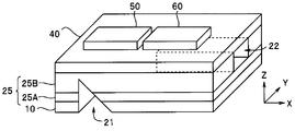
- FIGS. 1-3 ⁇ First Embodiment> ⁇ Configuration of optical transmission module 1>
- the optical transmission module 1 of 1st Embodiment is demonstrated using FIGS. 1-3.
- the drawings based on each embodiment are schematic, and the relationship between the thickness and width of each part, the thickness ratio of each part, and the like are different from the actual ones. It should be noted that the drawings may include portions having different dimensional relationships and ratios between the drawings. Further, illustration of some components (for example, an adhesive layer) is omitted.
- the Z-axis increasing direction in the drawing is referred to as an upward direction
- the Z-axis decreasing direction is referred to as a downward direction.
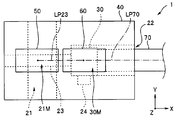
- the light transmission module 1 includes a light emitting element 50 that is a first optical element, a light receiving element 60 that is a second optical element, an optical waveguide substrate 20, a prism 30, and an optical fiber 70.
- a first substrate (hereinafter also referred to as “wiring board”) 40 on which the light emitting element 50 and the light receiving element 60 are mounted is disposed on the upper surface 20SA of the optical waveguide substrate 20, and a second substrate 10 is disposed on the lower surface 20SB.
- wiring board on which the light emitting element 50 and the light receiving element 60 are mounted is disposed on the upper surface 20SA of the optical waveguide substrate 20, and a second substrate 10 is disposed on the lower surface 20SB.
- the optical fiber 70 guides the third optical signal that is combined.
- the first wavelength ⁇ 1 is 850 nm
- the second wavelength ⁇ 2 is 1300 nm.
- the light emitting element 50 is a vertical cavity surface emitting laser (VCSEL: VerticalVerCavity Surface Emitting LASER), and in a direction perpendicular to the light emitting surface (XY plane) (Z-axis direction) according to an input drive electric signal.
- the light of the optical signal is emitted.
- an ultra-small light emitting element 50 having a size in plan view of 250 ⁇ m ⁇ 300 ⁇ m includes a light emitting unit 51 having a diameter of 20 ⁇ m and a connection terminal 52 that is electrically connected to the light emitting unit 51 and supplies an electric signal. On the light emitting surface.
- the light receiving element 60 is composed of a photodiode (PD) or the like, and converts an optical signal incident from a direction perpendicular to the light receiving surface (Z-axis direction) into an electric signal and outputs the electric signal.
- PD photodiode
- an ultra-small light receiving element 60 having a dimension in plan view of 350 ⁇ m ⁇ 300 ⁇ m includes a light receiving unit 61 having a diameter of 50 ⁇ m and a connection terminal 62 for outputting a received electrical signal electrically connected to the light receiving unit 61. Has on the light receiving surface.
- the optical waveguide substrate 20 is a polymer type optical waveguide substrate in which a clad 25 surrounds a core 23 that is an optical waveguide whose longitudinal direction is the X-axis direction for guiding an optical signal.
- the polymer type optical waveguide substrate 20 in which the core 23 and the clad 25 are made of resin is easier to process and more flexible than the optical waveguide substrate made of an inorganic material such as quartz.
- the optical transmission module 1 in which the flexible optical waveguide substrate 20 is sandwiched between the two flexible first substrates 40 and the second substrate 10 is flexible and can be disposed in a narrow space. Easy. That is, it is preferable that the first substrate 40 and the second substrate 10 have flexibility.
- the core 23 which is an optical waveguide is made of a first resin
- the clad 25 is made of a second resin having a refractive index smaller than that of the first resin.
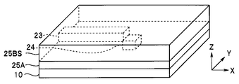
- the clad 25 includes a lower clad 25 ⁇ / b> A disposed under the core 23 and an upper clad 25 ⁇ / b> B surrounding the side surface and the upper surface of the core 23.
- the positioning member 24 made of the same first resin as the material of the core 23 is disposed in the same plane as the core 23. As will be described later, the core 23 and the positioning member 24 are simultaneously manufactured by patterning the core sheet 23S (see FIG. 5A).
- the light emitting element 50 and the light receiving element 60 are electrically connected to the electrode pads 43 and 44 of the wiring board 40, respectively.
- the wiring board 40 has a through hole 41 that becomes the optical path LP50 of the first optical signal and a through hole 42 that becomes the optical path LP60 of the second optical signal. Note that if the light transmittance of the wiring board 40 is high and the attenuation of the optical signal is within an allowable range, it is not necessary to form the through holes 41 and 42.
- the optical waveguide substrate 20 is provided with a groove 22 whose major axis direction is parallel to the major axis direction of the core 23 and whose section perpendicular to the major axis is rectangular.
- the groove 22 is an upper surface 25AS1 of the lower clad 25A with an opening on the top surface and a bottom surface on the bottom surface.
- the second end surface 23T2 of the core is exposed at the first wall surface 23S1 (see FIG. 3).
- the groove 22 becomes a hole having an opening on one side.
- a first reflecting surface 21M having an inclination angle of 45 degrees is formed on the first end surface 23T1 facing the second end surface 23T2 of the core 23.
- the first reflecting surface 21M is an inclined surface of the groove 21 formed from the lower surface side using a dicing blade.
- the first reflecting surface 21M reflects light incident on the core 23 from the vertical direction (Z-axis direction) by 90 degrees and guides it in the longitudinal direction (X-axis direction) of the core 23.
- the core 23 may be further extended from the first end face 23T1 at the time of manufacture.
- the outer side than the first reflecting surface 21M does not function as an optical waveguide, so the first reflecting surface 21M becomes an end surface of the core 23 that is an optical waveguide.
- a reflective film made of a metal such as gold may be formed on the wall surface of the groove 21, particularly the first reflective surface 21M, and the inside of the groove 21 is made of resin. It may be filled.
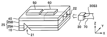
- the prism 30 and the optical fiber 70 are disposed in the groove 22.
- the prism 30 is a substantially rectangular parallelepiped having a rectangular shape in plan view, and has a second reflecting surface 30M having an inclination angle of 45 degrees.
- the second reflecting surface 30M transmits the first optical signal having the first wavelength, but reflects the optical path of the second optical signal having the second wavelength.
- the prism 30 is a dichroic right-angle prism having a reflecting surface 30M having a characteristic of transmitting light having a wavelength ⁇ 1 and reflecting light having a wavelength ⁇ 2.
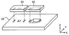
- a first substrate (wiring board) 40 on which a light emitting element 50 and a light receiving element 60 are mounted is disposed on the upper surface of the optical waveguide substrate 20.
- the first substrate 40 and the optical waveguide substrate 20 are positioned so that the light emitting element 50 and the light receiving element 60 are directly above the core 23.
- the first optical signal emitted (transmitted) by the light emitting element 50 in parallel with the Z axis is reflected by the first reflecting surface 21M in the X axis parallel direction and guided to the core 23.
- the first reflecting surface 21M optically couples the optical path LP50 of the light emitting element 50 orthogonal to the optical path LP23 of the core 23, which is a waveguide, with the optical path LP23.
- the first optical signal passes through the second reflecting surface 30M and enters the optical fiber 70.
- the second optical signal guided by the optical fiber 70 in the direction parallel to the X axis is reflected by the second reflecting surface 30M in the direction parallel to the Z axis, and enters the light receiving unit 61 of the light receiving element 60 and is received. Is done.
- the second reflecting surface 30M optically couples the optical path LP60 of the light receiving element 60 orthogonal to the optical path LP70 of the optical fiber 70 with the optical path LP70 of the optical fiber 70.
- the prism 30 disposed in the groove 22 has a second side surface (30S1, 30S2) that is perpendicular to the first wall surface 23S1 (see FIG. 3) or the first wall surface 23S1 of the groove 22, respectively.
- the position in the in-plane direction (XY direction) is defined by contacting the wall surface 24S1 (see FIG. 3).
- the prism 30 has a position in the vertical direction (Z direction) defined by the bottom surface 30SB contacting the top surface 25AS1 of the lower cladding 25A.
- the second wall surface 24S1 is one surface of the positioning member 24 made of the first resin. Since the positions of the two side surfaces (30S1, 30S2) and the bottom surface 30SB are defined, the prism 30 is accurately arranged at a predetermined position. For this reason, the light transmission module 1 has good light transmission efficiency.
- a lower clad sheet 25AS is laminated on the second substrate 10.
- the second substrate 10 an FPC substrate, a ceramic substrate, a glass epoxy substrate, a glass substrate, a silicon substrate, or the like is used, and a flexible substrate is preferable.
- the second substrate 10 is a support substrate for manufacturing the optical waveguide substrate 20 and is not an essential component of the optical transmission module 1.
- the second substrate 10 may be a wiring board having wiring or an electrode plate covered with a conductive film connected to a ground potential line.
- an adhesive layer may be provided therebetween.
- the lower clad sheet 25AS is a film made of a second resin that is the same material as the upper clad sheet 25BS (see FIG. 5C).
- the second resin is a resin having a lower refractive index than the first resin constituting the core 23.
- the second resin used also for the upper clad sheet 25BS to be patterned contains (A) a base polymer, (B) a photopolymerizable compound, and (C) a photopolymerization initiator. Is preferred.
- the lower clad 25 ⁇ / b> A and the upper clad 25 ⁇ / b> B do not necessarily have to be made of the same resin as long as each has a function as the clad 25.
- the lower clad sheet 25AS may not contain a photopolymerizable compound and a photopolymerization initiator.
- the base polymer is for ensuring the mechanical strength of the clad, and is made of a highly transparent resin such as a high-purity polyimide resin or polyether resin.
- the photopolymerizable compound is not particularly limited as long as it is polymerized by irradiation with light such as ultraviolet rays such as (meth) acrylate.
- light such as ultraviolet rays such as (meth) acrylate.
- photoinitiator For example, when a polymeric compound is an epoxy compound, it is an aryl diazonium salt.
- the present invention includes so-called additives such as an antioxidant, an anti-yellowing agent, an ultraviolet absorber, a visible light absorber, a colorant, a plasticizer, a stabilizer, and a filler. You may add in the ratio which does not have a bad influence on the effect of this.
- the lower clad sheet 25AS is produced by dissolving the above composition in a solvent, applying the solution to a support film, and removing the solvent.
- the lower cladding sheet 25AS and the upper cladding sheet 25BS preferably have a thickness of 5 ⁇ m or more and 500 ⁇ m or less.
- the thickness is 5 ⁇ m or more, the thickness of the clad necessary for light confinement can be secured, and when it is 500 ⁇ m or less, it is easy to make the thickness uniform.
- the lower clad sheet 25AS is cured by ultraviolet irradiation after lamination to become the lower clad 25A.
- the material of the lower clad sheet 25AS may be only a base polymer having no photosensitivity.
- the core sheet 23S made of the first resin to be the core 23 and the positioning member 24 is laminated on the lower clad 25A.
- the first resin has a refractive index higher than that of the second resin and can be patterned.
- the first resin has substantially the same composition as the second resin, and the refractive index is controlled by the molecular weight, the additive amount, and the like.
- the first resin and the second resin are made of the same polyimide, but the first resin has a refractive index of 1.555, and the second resin has a refractive index of 1.537.
- the thickness of the core sheet 23S is the height of the core 23 to be an optical waveguide. In order to ensure light guiding properties, the thickness of the core sheet 23S is preferably 5 ⁇ m or more and 100 ⁇ m or less.
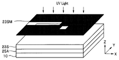
- FIG. 5A The core sheet 23S is irradiated (exposed) with ultraviolet rays through the negative photomask 23SM.
- the photomask 23SM is a negative mask in which areas corresponding to the shapes of the core 23 and the positioning member 24 are transparent. For this reason, ultraviolet rays are irradiated only to the region that becomes the core 23 and the positioning member 24, and the first resin in the region is polymerized.
- the core 23 and the positioning member 24 are simultaneously patterned by a photolithography method.
- the patterning step is not limited to the direct exposure method, but may be a selective polymerization method, a reactive ion etching (RIE) method, or a photobleaching method.
- RIE reactive ion etching
- the core 23 serving as an optical waveguide preferably has a width of 5 ⁇ m to 100 ⁇ m.
- the positioning member 24 has a side surface 24S1 orthogonal to the second end surface 23S1 of the core 23 at a predetermined position, the shape of the other portions is not particularly limited.
- the core sheet 23S made of a first resin made of polyethylene terephthalate or the like and arranged on a flexible and tough carrier film is patterned and then transferred onto the lower clad 25A to obtain the core 23 and the positioning member 24. May be provided.
- the upper clad sheet 25BS is laminated (laminated).
- the lower limit value of the thickness of the upper clad sheet 25BS needs to exceed (the value obtained by adding the thickness of the core sheet 23S and the thickness of the lower clad sheet 25AS).
- the thickness of the upper clad sheet 25BS is preferably (the lower limit value +10 ⁇ m or more and 100 ⁇ m) or less.
- the lower limit thickness of the upper clad sheet 25BS is 55 ⁇ m, preferably 65 ⁇ m or more and 155 ⁇ m or less.
- the upper clad sheet 25BS is patterned.
- the groove 22 is formed by a direct exposure method using a negative photomask.
- the light emitting element 50 and the light receiving element 60 are surface-mounted on the first substrate (first wiring board) 40. That is, the light emitting element 50 is flip-chip mounted on the first substrate 40 in a state where the light emitting unit 51 is disposed at a position facing the through hole 41 of the second substrate 40.
- the light receiving element 60 is flip-chip mounted on the first substrate 40 in a state where the light receiving portion 61 is disposed at a position facing the through hole 42 of the second substrate 40.
- an Au bump that is the connection terminal 52 of the light emitting element 50 is ultrasonically bonded to the electrode pad 43 of the second substrate 40.
- a sealing agent such as an underfill material or a sidefill material may be injected into the joint portion.
- a V-groove 21 is formed by using a dicing blade from the lower surface side (second substrate side) of the optical waveguide substrate 20 to which the second substrate 10 is bonded.
- the V groove 21 has a vertical surface and a first reflecting surface 21M having an inclination angle of 45 degrees.
- the V groove 21 has a depth that reaches the core 23.
- the core 23 is extended to the end surface of the optical waveguide substrate 20, and the groove 22 divides the core 23 to form the first reflecting surface 21M. For this reason, the core 23 and the clad 25 are also exposed on the vertical surface of the groove 22 in the same manner as the first reflecting surface 21M. However, the core 23 may be extended to the position of the first reflecting surface 21M of the V-groove 21, and all the vertical surfaces of the groove 22 may be exposed surfaces of the clad.
- the first substrate 40 is bonded to the main surface 20SA of the optical waveguide substrate 20. That is, the first substrate 40, which is a wiring board on which the light emitting element 50 and the light receiving element 60 are mounted, is disposed on the upper surface 20 SA of the optical waveguide substrate 20. The upper surface of the groove 22 is covered with the second substrate 40 to form a hole.
- a multimode optical fiber 70 having a diameter of 125 ⁇ m includes a core 71 having a diameter of 50 ⁇ m for transmitting light and a clad 72 covering the outer periphery of the core 71.
- the optical fiber 70 may be covered with an outer skin made of resin.
- the rectangular parallelepiped prism 30 has an upper surface 30SU, a lower surface 30SD, and four side surfaces 30S1 to 30S4. Then, the third side surface 30S3 of the prism 30 is bonded to the end surface of the optical fiber 70 with a light transmissive ultraviolet curable adhesive or the like.
- the second reflecting surface 30M having an inclination angle of 45 degrees of the prism 30 reflects the second light having the second wavelength in the upper surface direction. On the other hand, the second reflecting surface 30M transmits light of the first wavelength.
- Step S19> The prism 30 to which the optical fiber 70 is bonded is inserted from the opening on the side surface of the groove 22 and is fixed to the groove 22 by, for example, an ultraviolet curable transparent adhesive (not shown).
- the first side surface 30S1 of the prism 30 is in contact with the first wall surface 23S1 of the groove 22, and the second side surface 30S2 is orthogonal to the first wall surface 23S1. It arrange
- first resin of the core 23 and the positioning member 24 are exposed on the first wall surface 23S1 and the second wall surface 24S1 of the groove 22. It may not be easy to pattern the exposed surface of the first resin and the exposed surface of the second resin so that they completely form the same plane.
- the groove 22 is preferably patterned so that the core 23 and the positioning member 24 are convex.
- the first wall surface 23S1 of the groove 22 with which the side surface 30S1 of the prism 30 is in contact is a convex portion having a height D1 made of the core 23.
- the second wall surface 24S1 of the groove 22 with which the side surface 30S2 of the prism 30 abuts is a convex portion having a height D2 made of the positioning member 24. If the heights D1 and D2 of the recesses are 0.5 ⁇ m or more and 5 ⁇ m or less, the prism 30 can be accurately arranged.
- the position of the core 23 and the positioning member 24 is precisely defined by photolithography. For this reason, since the two side surfaces of the prism 30 are in contact with the second end surface 23S1 of the core 23 and the one surface 24S1 of the positioning member 24, the position in the horizontal direction (XY direction) can be easily and accurately defined.
- the optical transmission module 1 having good light transmission efficiency can be easily manufactured.
- the first optical element is the light emitting element 50
- the second optical element is the light receiving element 60.
- both the first optical element and the second optical element may be light receiving elements or light emitting elements.
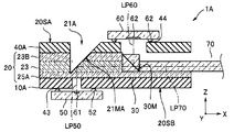
- optical transmission module 1A according to a modification of the first embodiment will be described. Since the optical transmission module 1A is similar to the optical transmission module 1, the same components are denoted by the same reference numerals and description thereof is omitted.
- the first substrate 40A on which the light receiving element 60 is mounted is disposed on the upper surface 20SA of the optical waveguide substrate 20, and the second substrate on which the light emitting element 50 is mounted.
- 10 ⁇ / b> A is disposed on the lower surface 20 ⁇ / b> SB of the optical waveguide substrate 20. That is, in the optical transmission module 1A, the second substrate 10A is a wiring board on which the electrode pads 43 are disposed.
- the first reflecting surface 21MA having an inclination angle of 45 degrees on the first end face of the core 23 is an inclined surface having an inclination angle of 45 degrees of the groove 21A formed from the upper surface side using a dicing blade.
- the first reflecting surface 21MA reflects light incident perpendicularly to the core 23 from below in the longitudinal direction of the core 23.
- the optical transmission module 1A has the same effect as the optical transmission module 1.
- the light transmission module in which the light emitting element 50 is mounted on the first substrate 40A and the light receiving element 60A is mounted on the second substrate 10A has the same effect as the light transmission module 1A.
- optical transmission module 1B of the second embodiment will be described. Since the optical transmission module 1B is similar to the optical transmission module 1, the same components are denoted by the same reference numerals and description thereof is omitted.
- the second reflecting surface 30MB of the prism 30B reflects the second optical signal guided by the optical fiber 70 in the in-plane orthogonal direction (Y direction).
- the elongated elongated positioning member has an optical waveguide function and constitutes the second core 24B.
- the end surface of the second core 24B has a third reflecting surface 29M having an oblique angle of 45 degrees.
- the third reflecting surface 29M is a wall surface of the V groove 21B2 having an inclined surface with an inclination angle of 45 degrees formed from the lower surface side (second substrate side) of the optical waveguide substrate 20B using a dicing blade. That is, the V groove 21 ⁇ / b> B ⁇ b> 2 is parallel to the groove 22 and orthogonal to the V groove 21.
- the light emitting element 50B is disposed immediately above the core 23, and the light receiving element 60B is disposed immediately above the second core 24B which is a positioning member extending in a direction orthogonal to the core 23.
- the second optical signal guided by the optical fiber 70 is reflected by the second reflecting surface 30MB of the prism 30B, guided to the second core 24B, and reflected by the third reflecting surface 29M to receive light.
- the light receiving element 60B is optically coupled to the optical fiber 70 via the third reflecting surface 29M, the second core 24B, and the second reflecting surface 30MB of the prism 30.
- the second core 24B which is a positioning member, is formed at a position facing the positioning member 24 of the optical transmission module 1.
- the prism 30B can easily arrange the positions of the two side surfaces and the bottom surface with high accuracy, and the optical transmission module 1A has the same effect as the optical transmission module 1, and moreover, The degree of freedom of arrangement of optical elements is higher than that of the transmission module 1, and miniaturization (especially shortening) is easy.
- both the first optical element and the second optical element may be light receiving elements or light emitting elements.
- the prism 30 is inserted and fixed from the opening formed in the first substrate 40B, and the fiber 70 is inserted and fixed from the groove 22, but the prism 30 and the fiber 70 are bonded and fixed. Later, it may be inserted and fixed from the groove 22. Further, an opening having the same shape as the groove 22 may be formed in the first substrate 40B, and the bonded prism 30 and the fiber 70 may be disposed and fixed from above the first substrate 40B.
- FIG. 10 shows the imaging module 2 including the light transmission module 1B.
- the imaging module 2 includes a cover glass (glass lid) 81, an imaging element 82, a T-shaped wiring board 83, an optical transmission module 1 ⁇ / b> B, and a cable 84.
- An image sensor 82 is mounted on a T-shaped wiring board 83, and a cable 84 is further connected.
- on the first substrate 40B of the optical transmission module 1B having the multiplexing / demultiplexing function not only the light emitting element 50B and the light receiving element 60B but also electronic components 86 such as a semiconductor IC (85) and a chip capacitor are surface-mounted. .
- a ball lens 87 that collects light is disposed on the end face of the optical fiber 70 of the optical transmission module 1B.
- the light transmission module 1B is disposed on a wiring board 83 that transmits and receives electrical signals to and from the image sensor 82.
- the first wiring board 40B of the optical transmission module 1B is connected to the wiring board 83 by a through wiring 28 that penetrates the optical waveguide substrate 20B and the second wiring board 10B.
- the light receiving element 60B receives the second optical signal guided through the optical fiber 70, converts it into an electrical signal, and transmits it to the imaging element 82.
- the imaging signal from the imaging element 82 is converted into a first optical signal by the light emitting element 50 ⁇ / b> B and guided through the optical fiber 70.
- the clock signal converted into the second optical signal having the wavelength ⁇ 2 enters the optical transmission module 1B including the multiplexer / demultiplexer from the optical fiber 70, and is received by the light receiving element 60B.
- the received second optical signal is photoelectrically converted into an electrical signal and input to the image sensor 82 as a clock signal.
- the imaging signal output from the imaging element 82 is converted into a first optical signal having a wavelength ⁇ 1 by the light emitting element 50B and guided to the optical fiber 70.
- the imaging module 2 can be easily reduced in size by converting the input / output signals of the imaging element 82 into light by the optical transmission module 1B having a small multiplexing / demultiplexing function and multiplexing the light.
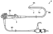
- the endoscope 9 includes an insertion portion 9B in which the imaging module 2 is disposed at the distal end portion 9A, an operation portion 9C disposed on the proximal end side of the insertion portion 9B, and an operation portion 9C. And a universal cord 9D extending from.
- the optical signal guided by the optical fiber 70 inserted through the insertion portion 9B is converted into an electrical signal by the imaging module 3 provided in the operation portion 9C.
- the distal end portion 9A has a small diameter.
Landscapes
- Health & Medical Sciences (AREA)
- Life Sciences & Earth Sciences (AREA)
- Physics & Mathematics (AREA)
- Surgery (AREA)
- Optics & Photonics (AREA)
- Engineering & Computer Science (AREA)
- Biomedical Technology (AREA)
- Veterinary Medicine (AREA)
- Biophysics (AREA)
- Pathology (AREA)
- Radiology & Medical Imaging (AREA)
- Nuclear Medicine, Radiotherapy & Molecular Imaging (AREA)
- Public Health (AREA)
- Heart & Thoracic Surgery (AREA)
- Medical Informatics (AREA)
- Molecular Biology (AREA)
- Animal Behavior & Ethology (AREA)
- General Health & Medical Sciences (AREA)
- General Physics & Mathematics (AREA)
- Microelectronics & Electronic Packaging (AREA)
- Multimedia (AREA)
- Signal Processing (AREA)
- Optical Couplings Of Light Guides (AREA)
- Optical Integrated Circuits (AREA)
- Endoscopes (AREA)
- Instruments For Viewing The Inside Of Hollow Bodies (AREA)
Abstract
Description
<光伝送モジュール1の構成>
図1から図3を用いて第1実施形態の光伝送モジュール1について説明する。なお、以下の説明において、各実施の形態に基づく図面は、模式的なものであり、各部分の厚みと幅との関係、夫々の部分の厚みの比率などは現実のものとは異なることに留意すべきであり、図面の相互間においても互いの寸法の関係や比率が異なる部分が含まれている場合がある。また一部の構成要素(例えば接着層)の図示を省略する。なお、以下、図面のZ軸増加方向を上方向、Z軸減少方向を下方向という。
次に、図4のフローチャートに沿って、光伝送モジュール1の製造方法を説明する。
第2基板10の上に、下部クラッドシート25ASがラミネートされる。第2基板10には、FPC基板、セラミック基板、ガラスエポキシ基板、ガラス基板、シリコン基板等が使用されるが、可撓性基板であることが好ましい。なお、第2基板10は光導波路基板20を製造するためのサポート基板であり、光伝送モジュール1の必須の構成要素ではない。また、第2基板10は、配線を有する配線板、または、接地電位線と接続された導電膜で覆われた電極板であってもよい。
ネガ型フォトマスク23SMを介してコアシート23Sに紫外線が照射(露光)される。
現像処理により、紫外線が照射されなかった領域の第1の樹脂が溶解し、コア23および位置決め部材24が同時に形成される。
上部クラッドシート25BSが積層(ラミネート)される。コア23を覆うために、上部クラッドシート25BSの厚さ下限値は、(コアシート23Sの厚さと下部クラッドシート25ASの厚さとを加算した値)超とする必要がある。上部クラッドシート25BSの厚さは、(前記下限値+10μm以上100μm)以下が好ましい。例えば、下部クラッドシート25ASの厚さが30μm、コアシート23Sの厚さが25μmの場合、上部クラッドシート25BSの下限厚さは55μmであるが、好ましくは65μm以上155μm以下である。
上部クラッド25Bに所定の溝22を形成するため、上部クラッドシート25BSのパターニングが行われる。例えば、ネガ型フォトマスクを用いた直接露光法により溝22が形成される。
一方、第2基板10が接着された光導波路基板20の下面側(第2基板側)から、ダイシングブレードを用いてV溝21が形成される。V溝21は、垂直面と、傾斜角度45度の第1の反射面21Mとを有する。そして、V溝21はコア23に到達する深さを有する。
第1基板40が光導波路基板20の主面20SAに接着される。すなわち、発光素子50および受光素子60が実装された配線板である第1基板40が、光導波路基板20の上面20SAに配設される。溝22は上面が第2基板40で覆われて穴となる。
プリズム30に光ファイバ70が接着される。例えば、径が125μmのマルチモード型の光ファイバ70は、光を伝送する径が50μmのコア71と、コア71の外周を覆うクラッド72とからなる。光ファイバ70は、樹脂からなる外皮に覆われていてもよい。
光ファイバ70が接着されたプリズム30が、溝22の側面の開口から挿入され、例えば紫外線硬化型の透明接着剤(不図示)により溝22に固定される。このとき、図6に示すように、プリズム30の第1の側面30S1が溝22の第1の壁面23S1と当接するように、かつ、第2の側面30S2が、第1の壁面23S1と直交する第2の壁面24S1と当接するように配置される。
次に第1実施形態の変形例の光伝送モジュール1Aについて説明する。光伝送モジュール1Aは、光伝送モジュール1と類似しているので、同じ構成要素には同じ符号を付し説明は省略する。
次に第2実施形態の光伝送モジュール1Bについて説明する。光伝送モジュール1Bは、光伝送モジュール1と類似しているので、同じ構成要素には同じ符号を付し説明は省略する。
次に、第3の実施の形態の内視鏡9について説明する。
2・・・撮像モジュール
9・・・内視鏡
10・・・第2基板
20・・・光導波路基板
21・・・V溝
22・・・溝
23・・・コア(光導波路)
24・・・位置決め部材
25・・・クラッド
30・・・プリズム
40・・・配線板(第1基板)
50・・・発光素子
60・・・受光素子
70・・・光ファイバ
Claims (12)
- 第1の光信号を送信または受信する第1の光素子と、
第2の光信号を送信または受信する第2の光素子と、
前記第1の光信号と前記第2の光信号とが合波された第3の光信号を導光する光ファイバと、
第1の樹脂からなる光導波路を有し、前記光導波路が第1の端面に傾斜角45度の第1の反射面を有し、第2の端面が前記光ファイバの光路と光結合している、光導波路基板と、を具備する光伝送モジュールであって、
前記光導波路基板に形成された溝に、前記光ファイバおよび前記第1の光信号が透過する傾斜角45度の第2の反射面を有するプリズムが配設されており、
前記光導波路の光路と、前記光導波路の前記光路に対して直交している前記第1の光素子の光路とが、前記第1の反射面を介して光結合しており、
前記光ファイバの前記光路と、前記光ファイバの前記光路に対して直交している前記第2の光素子の光路とが、前記第2の反射面を介して光結合しており、
前記溝の第1の壁面に前記光導波路の前記第2の端面が露出しており、前記溝の第2の壁面に前記第1の樹脂からなる位置決め部材の一面が露出しており、
前記プリズムの第1の側面が、前記溝の第1の壁面と当接しており、第2の側面が前記溝の第2の壁面と当接していることを特徴とする光伝送モジュール。 - 前記第1の側面が前記光導波路の凸部と当接しており、前記第2の側面が前記位置決め部材の凸部と当接していることを特徴とする請求項1に記載の光伝送モジュール。
- 前記第1の光素子および前記第2の光素子が実装された第1基板が、前記光導波路基板の上面に配設されていることを特徴とする請求項2に記載の光伝送モジュール。
- 前記第1の光素子が実装された第1基板が、前記光導波路基板の上面に配設されており、
前記第2の光素子が実装された第2基板が、前記導波路基板の下面に配設されていることを特徴とする請求項2に記載の光伝送モジュール。 - 前記第1の光素子および前記第2の光素子が、それぞれ前記光導波路の直上または直下に配設されていることを特徴とする請求項1から請求項4のいずれか1項に記載の光伝送モジュール。
- 前記第1の光素子が前記光導波路の直上または直下に配設されており、
前記位置決め部材が、直交する方向に延設され、端面に傾斜角45度の第3の反射面がる第2の光導波路を構成しており、
前記第2の光導波路の直上に配設されている前記第2の光素子が、前記第3の反射面、前記第2の光導波路、および前記プリズムを介して前記光ファイバと光結合していることを特徴とする請求項1から請求項4のいずれか1項に記載の光伝送モジュール。 - 前記第1の光素子が発光素子で、
前記第2の光素子が受光素子であることを特徴とする請求項1から請求項6のいずれか1項に記載の光伝送モジュール。 - 前記第1の光素子および前記第2の光素子が発光素子で、あることを特徴とする請求項1から請求項6のいずれか1項に記載の光伝送モジュール。
- 前記第1の光素子および前記第2の光素子が受光素子で、あることを特徴とする請求項1から請求項6のいずれか1項に記載の光伝送モジュール。
- 請求項1から請求項9のいずれか1項に記載の光伝送モジュールを挿入部の先端部に具備することを特徴とする内視鏡。
- 請求項1から請求項9のいずれか1項に記載の光伝送モジュールの製造方法であって、
前記光導波路と前記位置決め部材とが、フォトリソグラフィ法により同時にパターニングされる工程を具備することを特徴とする光伝送モジュールの製造方法。 - 前記プリズムに前記光ファイバを接着する工程のあとに、前記光ファイバが接着された前記プリズムを前記溝の所定位置に配設する工程が行われることを特徴とする請求項11に記載の光伝送モジュールの製造方法。
Priority Applications (5)
| Application Number | Priority Date | Filing Date | Title |
|---|---|---|---|
| CN201580077993.5A CN107407782A (zh) | 2015-03-20 | 2015-03-20 | 光传送模块、内窥镜以及所述光传送模块的制造方法 |
| PCT/JP2015/058448 WO2016151670A1 (ja) | 2015-03-20 | 2015-03-20 | 光伝送モジュール、内視鏡、および前記光伝送モジュールの製造方法 |
| JP2017507139A JP6445138B2 (ja) | 2015-03-20 | 2015-03-20 | 光伝送モジュール、内視鏡、および前記光伝送モジュールの製造方法 |
| DE112015006339.0T DE112015006339T5 (de) | 2015-03-20 | 2015-03-20 | Optisches Übertragungsmodul, Endoskop und Verfahren zur Herstellung eines optischen Übertragungsmoduls |
| US15/710,134 US9952391B2 (en) | 2015-03-20 | 2017-09-20 | Optical transmission module, endoscope, and method for manufacturing optical transmission module |
Applications Claiming Priority (1)
| Application Number | Priority Date | Filing Date | Title |
|---|---|---|---|
| PCT/JP2015/058448 WO2016151670A1 (ja) | 2015-03-20 | 2015-03-20 | 光伝送モジュール、内視鏡、および前記光伝送モジュールの製造方法 |
Related Child Applications (1)
| Application Number | Title | Priority Date | Filing Date |
|---|---|---|---|
| US15/710,134 Continuation US9952391B2 (en) | 2015-03-20 | 2017-09-20 | Optical transmission module, endoscope, and method for manufacturing optical transmission module |
Publications (1)
| Publication Number | Publication Date |
|---|---|
| WO2016151670A1 true WO2016151670A1 (ja) | 2016-09-29 |
Family
ID=56977228
Family Applications (1)
| Application Number | Title | Priority Date | Filing Date |
|---|---|---|---|
| PCT/JP2015/058448 Ceased WO2016151670A1 (ja) | 2015-03-20 | 2015-03-20 | 光伝送モジュール、内視鏡、および前記光伝送モジュールの製造方法 |
Country Status (5)
| Country | Link |
|---|---|
| US (1) | US9952391B2 (ja) |
| JP (1) | JP6445138B2 (ja) |
| CN (1) | CN107407782A (ja) |
| DE (1) | DE112015006339T5 (ja) |
| WO (1) | WO2016151670A1 (ja) |
Cited By (4)
| Publication number | Priority date | Publication date | Assignee | Title |
|---|---|---|---|---|
| WO2019207650A1 (ja) * | 2018-04-24 | 2019-10-31 | オリンパス株式会社 | 内視鏡用撮像装置、内視鏡、および内視鏡用撮像装置の製造方法 |
| JP2019197081A (ja) * | 2018-05-07 | 2019-11-14 | ファナック株式会社 | レーザ発振器 |
| WO2021176596A1 (ja) * | 2020-03-04 | 2021-09-10 | オリンパス株式会社 | 内視鏡用撮像装置、および、内視鏡 |
| WO2024143134A1 (ja) * | 2022-12-28 | 2024-07-04 | 京セラ株式会社 | 光回路基板、光学部品実装構造体および光回路基板の製造方法 |
Families Citing this family (13)
| Publication number | Priority date | Publication date | Assignee | Title |
|---|---|---|---|---|
| US10168494B2 (en) | 2016-11-30 | 2019-01-01 | International Business Machines Corporation | Off-axis micro-mirror arrays for optical coupling in polymer waveguides |
| JP2018105907A (ja) * | 2016-12-22 | 2018-07-05 | オリンパス株式会社 | 光モジュールおよび内視鏡 |
| WO2018173261A1 (ja) * | 2017-03-24 | 2018-09-27 | オリンパス株式会社 | 内視鏡および光電複合モジュール |
| WO2018198247A1 (ja) * | 2017-04-26 | 2018-11-01 | オリンパス株式会社 | 内視鏡、撮像モジュール、および、撮像モジュールの製造方法 |
| WO2019077643A1 (ja) * | 2017-10-16 | 2019-04-25 | オリンパス株式会社 | 内視鏡および内視鏡システム |
| WO2020010585A1 (zh) * | 2018-07-12 | 2020-01-16 | 华为技术有限公司 | 光耦合装置及其封装方法、光模块及通讯设备 |
| CN109387910A (zh) * | 2018-11-09 | 2019-02-26 | 中国电子科技集团公司第三十研究所 | 一种并行光收发引擎组件 |
| TWM576855U (zh) * | 2018-12-12 | 2019-04-21 | 榮晶生物科技股份有限公司 | Endoscope device and its cable assembly |
| WO2021158500A1 (en) * | 2020-02-03 | 2021-08-12 | Lightmatter, Inc. | Photonic wafer communication systems and related packages |
| TW202132835A (zh) * | 2020-02-21 | 2021-09-01 | 合聖科技股份有限公司 | 單向傳輸裝置及信號單向傳輸方法 |
| CN114520217A (zh) * | 2020-11-18 | 2022-05-20 | 芯巧科技股份有限公司 | 具光耦特性的电子元件的改良结构 |
| JP7687926B2 (ja) * | 2021-10-01 | 2025-06-03 | Hoya株式会社 | 光送信モジュールおよび内視鏡 |
| CN115390201B (zh) * | 2022-09-22 | 2024-02-23 | 希烽光电科技(南京)有限公司 | 低变形高可靠性光发射组件 |
Citations (4)
| Publication number | Priority date | Publication date | Assignee | Title |
|---|---|---|---|---|
| JPH0262502A (ja) * | 1988-08-30 | 1990-03-02 | Asahi Chem Ind Co Ltd | 新規なる光デバイス |
| JPH06151903A (ja) * | 1992-11-13 | 1994-05-31 | Fujitsu Ltd | 光/電変換素子・光ファイバ結合モジュール |
| JP2009162882A (ja) * | 2007-12-28 | 2009-07-23 | Hitachi Cable Ltd | 光伝送アセンブリ |
| JP2012113031A (ja) * | 2010-11-22 | 2012-06-14 | Hitachi Chem Co Ltd | 光ファイバコネクタ及びその製造方法 |
Family Cites Families (6)
| Publication number | Priority date | Publication date | Assignee | Title |
|---|---|---|---|---|
| JP2956332B2 (ja) * | 1991-12-24 | 1999-10-04 | 日本電気株式会社 | 光半導体モジュール |
| KR100211985B1 (ko) * | 1996-12-11 | 1999-08-02 | 이계철 | 하이브리드 광집적회로용 마이크로 거울, 그의 제조방법, 마이크로 거울-광검출기 어셈블리 및 광수신용 하이브리드 광집적회로 어셈블리 |
| JP4012785B2 (ja) * | 2002-08-27 | 2007-11-21 | 日本板硝子株式会社 | 光接続装置 |
| TWI246612B (en) * | 2004-10-12 | 2006-01-01 | Phoenix Prec Technology Corp | Structure having embedded optical electronic components |
| JP2008250007A (ja) | 2007-03-30 | 2008-10-16 | Fuji Xerox Co Ltd | 光電子回路基板 |
| CN102753082B (zh) * | 2010-10-26 | 2016-10-12 | 奥林巴斯株式会社 | 内窥镜 |
-
2015
- 2015-03-20 JP JP2017507139A patent/JP6445138B2/ja active Active
- 2015-03-20 CN CN201580077993.5A patent/CN107407782A/zh active Pending
- 2015-03-20 WO PCT/JP2015/058448 patent/WO2016151670A1/ja not_active Ceased
- 2015-03-20 DE DE112015006339.0T patent/DE112015006339T5/de not_active Withdrawn
-
2017
- 2017-09-20 US US15/710,134 patent/US9952391B2/en active Active
Patent Citations (4)
| Publication number | Priority date | Publication date | Assignee | Title |
|---|---|---|---|---|
| JPH0262502A (ja) * | 1988-08-30 | 1990-03-02 | Asahi Chem Ind Co Ltd | 新規なる光デバイス |
| JPH06151903A (ja) * | 1992-11-13 | 1994-05-31 | Fujitsu Ltd | 光/電変換素子・光ファイバ結合モジュール |
| JP2009162882A (ja) * | 2007-12-28 | 2009-07-23 | Hitachi Cable Ltd | 光伝送アセンブリ |
| JP2012113031A (ja) * | 2010-11-22 | 2012-06-14 | Hitachi Chem Co Ltd | 光ファイバコネクタ及びその製造方法 |
Cited By (6)
| Publication number | Priority date | Publication date | Assignee | Title |
|---|---|---|---|---|
| WO2019207650A1 (ja) * | 2018-04-24 | 2019-10-31 | オリンパス株式会社 | 内視鏡用撮像装置、内視鏡、および内視鏡用撮像装置の製造方法 |
| US11435570B2 (en) | 2018-04-24 | 2022-09-06 | Olympus Corporation | Image pickup apparatus for endoscope, endoscope, and manufacturing method of image pickup apparatus for endoscope |
| JP2019197081A (ja) * | 2018-05-07 | 2019-11-14 | ファナック株式会社 | レーザ発振器 |
| US10734783B2 (en) | 2018-05-07 | 2020-08-04 | Fanuc Corporation | Laser oscillator |
| WO2021176596A1 (ja) * | 2020-03-04 | 2021-09-10 | オリンパス株式会社 | 内視鏡用撮像装置、および、内視鏡 |
| WO2024143134A1 (ja) * | 2022-12-28 | 2024-07-04 | 京セラ株式会社 | 光回路基板、光学部品実装構造体および光回路基板の製造方法 |
Also Published As
| Publication number | Publication date |
|---|---|
| US9952391B2 (en) | 2018-04-24 |
| US20180008132A1 (en) | 2018-01-11 |
| CN107407782A (zh) | 2017-11-28 |
| JPWO2016151670A1 (ja) | 2018-01-11 |
| JP6445138B2 (ja) | 2018-12-26 |
| DE112015006339T5 (de) | 2017-11-30 |
Similar Documents
| Publication | Publication Date | Title |
|---|---|---|
| JP6445138B2 (ja) | 光伝送モジュール、内視鏡、および前記光伝送モジュールの製造方法 | |
| JP6461786B2 (ja) | 光電気混載デバイス及びその製造方法 | |
| US7590315B2 (en) | Optical waveguide and optical module using the same | |
| US8311375B2 (en) | Optoelectronic wiring board, optical communication device, and method of manufacturing the optical communication device | |
| JP4845333B2 (ja) | 光電変換素子パッケージ、その作製方法及び光コネクタ | |
| JP6659826B2 (ja) | 光伝送モジュール及び内視鏡 | |
| US20180011263A1 (en) | Optical transmission module and endoscope | |
| JP5395042B2 (ja) | 光路変換デバイスの製造方法 | |
| JP5849220B2 (ja) | 光モジュール | |
| KR101256814B1 (ko) | 완전 수동정렬 패키징된 광모듈 및 그 제조방법 | |
| JP5737199B2 (ja) | 光モジュール及びその製造方法 | |
| JP2005338704A (ja) | 光結合機能付配線基板及びその製造方法と光結合システム | |
| JP5144357B2 (ja) | 複合光伝送基板および光モジュール | |
| JP2012088634A (ja) | 光導波路デバイス及びその製造方法 | |
| JP4607063B2 (ja) | 光路変換コネクタの製造方法 | |
| JP6551808B2 (ja) | 内視鏡、光伝送モジュールおよび光伝送モジュールの製造方法 | |
| JP6137971B2 (ja) | 光導波路付きフレキシブルプリント配線板、およびその製造方法 | |
| JP4800409B2 (ja) | 光路変換コネクタの製造方法 | |
| WO2017115413A1 (ja) | 光伝送モジュールおよび内視鏡 | |
| JP5047591B2 (ja) | フレキシブル光導波路および光導波路モジュール | |
| WO2017179149A1 (ja) | 内視鏡用光伝送モジュールの製造方法および内視鏡 | |
| JP2020056894A (ja) | 光路変換部品、光路変換部品付き光導波路、光モジュールおよび電子機器 | |
| JP5279931B2 (ja) | 複合光伝送基板および光モジュール | |
| JP2024060736A (ja) | 光接続構造、光モジュール | |
| WO2017115412A1 (ja) | 光伝送モジュールおよび内視鏡 |
Legal Events
| Date | Code | Title | Description |
|---|---|---|---|
| 121 | Ep: the epo has been informed by wipo that ep was designated in this application |
Ref document number: 15886227 Country of ref document: EP Kind code of ref document: A1 |
|
| ENP | Entry into the national phase |
Ref document number: 2017507139 Country of ref document: JP Kind code of ref document: A |
|
| WWE | Wipo information: entry into national phase |
Ref document number: 112015006339 Country of ref document: DE |
|
| 122 | Ep: pct application non-entry in european phase |
Ref document number: 15886227 Country of ref document: EP Kind code of ref document: A1 |