WO2016148110A1 - 半導体ウェハ加工用粘着テープ - Google Patents
半導体ウェハ加工用粘着テープ Download PDFInfo
- Publication number
- WO2016148110A1 WO2016148110A1 PCT/JP2016/058005 JP2016058005W WO2016148110A1 WO 2016148110 A1 WO2016148110 A1 WO 2016148110A1 JP 2016058005 W JP2016058005 W JP 2016058005W WO 2016148110 A1 WO2016148110 A1 WO 2016148110A1
- Authority
- WO
- WIPO (PCT)
- Prior art keywords
- adhesive tape
- semiconductor wafer
- parts
- pressure
- sensitive adhesive
- Prior art date
- Legal status (The legal status is an assumption and is not a legal conclusion. Google has not performed a legal analysis and makes no representation as to the accuracy of the status listed.)
- Ceased
Links
Images


Classifications
-
- C—CHEMISTRY; METALLURGY
- C09—DYES; PAINTS; POLISHES; NATURAL RESINS; ADHESIVES; COMPOSITIONS NOT OTHERWISE PROVIDED FOR; APPLICATIONS OF MATERIALS NOT OTHERWISE PROVIDED FOR
- C09J—ADHESIVES; NON-MECHANICAL ASPECTS OF ADHESIVE PROCESSES IN GENERAL; ADHESIVE PROCESSES NOT PROVIDED FOR ELSEWHERE; USE OF MATERIALS AS ADHESIVES
- C09J7/00—Adhesives in the form of films or foils
- C09J7/20—Adhesives in the form of films or foils characterised by their carriers
- C09J7/29—Laminated material
-
- C—CHEMISTRY; METALLURGY
- C09—DYES; PAINTS; POLISHES; NATURAL RESINS; ADHESIVES; COMPOSITIONS NOT OTHERWISE PROVIDED FOR; APPLICATIONS OF MATERIALS NOT OTHERWISE PROVIDED FOR
- C09J—ADHESIVES; NON-MECHANICAL ASPECTS OF ADHESIVE PROCESSES IN GENERAL; ADHESIVE PROCESSES NOT PROVIDED FOR ELSEWHERE; USE OF MATERIALS AS ADHESIVES
- C09J201/00—Adhesives based on unspecified macromolecular compounds
-
- C—CHEMISTRY; METALLURGY
- C09—DYES; PAINTS; POLISHES; NATURAL RESINS; ADHESIVES; COMPOSITIONS NOT OTHERWISE PROVIDED FOR; APPLICATIONS OF MATERIALS NOT OTHERWISE PROVIDED FOR
- C09J—ADHESIVES; NON-MECHANICAL ASPECTS OF ADHESIVE PROCESSES IN GENERAL; ADHESIVE PROCESSES NOT PROVIDED FOR ELSEWHERE; USE OF MATERIALS AS ADHESIVES
- C09J4/00—Adhesives based on organic non-macromolecular compounds having at least one polymerisable carbon-to-carbon unsaturated bond ; adhesives, based on monomers of macromolecular compounds of groups C09J183/00 - C09J183/16
-
- C—CHEMISTRY; METALLURGY
- C09—DYES; PAINTS; POLISHES; NATURAL RESINS; ADHESIVES; COMPOSITIONS NOT OTHERWISE PROVIDED FOR; APPLICATIONS OF MATERIALS NOT OTHERWISE PROVIDED FOR
- C09J—ADHESIVES; NON-MECHANICAL ASPECTS OF ADHESIVE PROCESSES IN GENERAL; ADHESIVE PROCESSES NOT PROVIDED FOR ELSEWHERE; USE OF MATERIALS AS ADHESIVES
- C09J5/00—Adhesive processes in general; Adhesive processes not provided for elsewhere, e.g. relating to primers
-
- C—CHEMISTRY; METALLURGY
- C09—DYES; PAINTS; POLISHES; NATURAL RESINS; ADHESIVES; COMPOSITIONS NOT OTHERWISE PROVIDED FOR; APPLICATIONS OF MATERIALS NOT OTHERWISE PROVIDED FOR
- C09J—ADHESIVES; NON-MECHANICAL ASPECTS OF ADHESIVE PROCESSES IN GENERAL; ADHESIVE PROCESSES NOT PROVIDED FOR ELSEWHERE; USE OF MATERIALS AS ADHESIVES
- C09J7/00—Adhesives in the form of films or foils
- C09J7/20—Adhesives in the form of films or foils characterised by their carriers
-
- C—CHEMISTRY; METALLURGY
- C09—DYES; PAINTS; POLISHES; NATURAL RESINS; ADHESIVES; COMPOSITIONS NOT OTHERWISE PROVIDED FOR; APPLICATIONS OF MATERIALS NOT OTHERWISE PROVIDED FOR
- C09J—ADHESIVES; NON-MECHANICAL ASPECTS OF ADHESIVE PROCESSES IN GENERAL; ADHESIVE PROCESSES NOT PROVIDED FOR ELSEWHERE; USE OF MATERIALS AS ADHESIVES
- C09J7/00—Adhesives in the form of films or foils
- C09J7/30—Adhesives in the form of films or foils characterised by the adhesive composition
-
- H—ELECTRICITY
- H10—SEMICONDUCTOR DEVICES; ELECTRIC SOLID-STATE DEVICES NOT OTHERWISE PROVIDED FOR
- H10P—GENERIC PROCESSES OR APPARATUS FOR THE MANUFACTURE OR TREATMENT OF DEVICES COVERED BY CLASS H10
- H10P52/00—Grinding, lapping or polishing of wafers, substrates or parts of devices
-
- H—ELECTRICITY
- H10—SEMICONDUCTOR DEVICES; ELECTRIC SOLID-STATE DEVICES NOT OTHERWISE PROVIDED FOR
- H10P—GENERIC PROCESSES OR APPARATUS FOR THE MANUFACTURE OR TREATMENT OF DEVICES COVERED BY CLASS H10
- H10P72/00—Handling or holding of wafers, substrates or devices during manufacture or treatment thereof
- H10P72/04—Apparatus for manufacture or treatment
- H10P72/0442—Apparatus for placing on an insulating substrate, e.g. tape
-
- H—ELECTRICITY
- H10—SEMICONDUCTOR DEVICES; ELECTRIC SOLID-STATE DEVICES NOT OTHERWISE PROVIDED FOR
- H10P—GENERIC PROCESSES OR APPARATUS FOR THE MANUFACTURE OR TREATMENT OF DEVICES COVERED BY CLASS H10
- H10P72/00—Handling or holding of wafers, substrates or devices during manufacture or treatment thereof
- H10P72/70—Handling or holding of wafers, substrates or devices during manufacture or treatment thereof for supporting or gripping
- H10P72/74—Handling or holding of wafers, substrates or devices during manufacture or treatment thereof for supporting or gripping using temporarily an auxiliary support
- H10P72/7402—Wafer tapes, e.g. grinding or dicing support tapes
-
- C—CHEMISTRY; METALLURGY
- C09—DYES; PAINTS; POLISHES; NATURAL RESINS; ADHESIVES; COMPOSITIONS NOT OTHERWISE PROVIDED FOR; APPLICATIONS OF MATERIALS NOT OTHERWISE PROVIDED FOR
- C09J—ADHESIVES; NON-MECHANICAL ASPECTS OF ADHESIVE PROCESSES IN GENERAL; ADHESIVE PROCESSES NOT PROVIDED FOR ELSEWHERE; USE OF MATERIALS AS ADHESIVES
- C09J2203/00—Applications of adhesives in processes or use of adhesives in the form of films or foils
- C09J2203/326—Applications of adhesives in processes or use of adhesives in the form of films or foils for bonding electronic components such as wafers, chips or semiconductors
Definitions
- the present invention relates to an adhesive tape used for processing a semiconductor device, and more particularly to a surface protective adhesive tape for semiconductor processing suitable for use when grinding a back surface of a semiconductor wafer.
- a surface protective adhesive tape is bonded to the wafer surface, and the wafer back surface is ground in that state.
- a pressure-sensitive adhesive layer mainly composed of an acrylic polymer is provided on a plastic film such as polyolefin has been proposed (for example, see Patent Document 1).
- the pressure-sensitive adhesive constituting the pressure-sensitive adhesive layer an energy ray-curable pressure-sensitive adhesive that reduces the adhesive force by irradiation with energy rays and facilitates tape peeling from the wafer is used.
- the energy ray curable pressure-sensitive adhesive has an energy ray curable double bond as its component.
- This double bond may exist in the molecule of the acrylic polymer or may exist as a molecule different from the polymer, for example, an oligomer having a double bond.
- the curing by energy ray irradiation may not be completed even if the tackiness of the adhesive (hereinafter referred to as tack force) disappears.
- tack force tackiness of the adhesive
- adhesive residue an adhesive residue (hereinafter referred to as adhesive residue) is generated on the wafer surface due to poor curing.
- the present invention solves the above-mentioned problems, and in semiconductor wafer processing, particularly in a back grinding process of a silicon wafer or the like, a semiconductor that does not generate adhesive residue when the semiconductor processing adhesive tape is peeled off from the wafer surface after back polishing.
- An object is to provide an adhesive tape for processing.
- the present inventor has found that the adhesive layer is effective in reducing adhesive residue when there is a change in physical properties due to energy ray irradiation.
- the present invention has been made based on this finding.
- an adhesive tape for processing a semiconductor wafer has a base film and an energy ray-curable adhesive layer provided on one side of the base film.
- the adhesive strength before irradiation is A (N / 25 mm)
- the tack force is T (KPa)
- the elongation is E (mm)
- the adhesive strength after irradiation with energy rays is A UV (N / 25 mm)
- the tack force is When T UV (KPa) and elongation are E UV (mm), A UV /A ⁇ 0.3, T UV /T ⁇ 0.05, and E UV /E ⁇ 0.3 It is characterized by being.
- the base film includes a plurality of resin layers made of at least one resin selected from polyethylene and an ethylene copolymer, and the resin layer in contact with the pressure-sensitive adhesive layer has a vinyl acetate content of 5 to 20% by mass.
- the outermost resin layer opposite to the pressure-sensitive adhesive layer is made of an ethylene vinyl acetate copolymer, and is characterized by being made of polyethylene or an ethylene vinyl acetate copolymer having a vinyl acetate content of 10% by mass or less.
- the pressure-sensitive adhesive layer preferably has a thickness of 20 to 40 ⁇ m and contains an energy ray reactive release agent.
- the pressure-sensitive adhesive tape for processing a semiconductor wafer according to the present invention is preferably used for back grinding of a semiconductor wafer having a circuit formed on the surface.
- a semiconductor processing pressure-sensitive adhesive tape that does not generate adhesive residue when the semiconductor processing pressure-sensitive adhesive tape is peeled off from the wafer surface after back surface polishing in the processing of semiconductor wafers, particularly in the back surface grinding process of silicon wafers and the like. Can do.
- the semiconductor wafer processing pressure-sensitive adhesive tape has a pressure-sensitive adhesive layer made of at least one energy ray-curable pressure-sensitive adhesive on one side of the base film.
- FIG. 1 is a schematic sectional view showing a preferred embodiment of the adhesive tape 1 for protecting a semiconductor surface of the present invention.
- the semiconductor surface protecting adhesive tape 1 has a base film 2, and an adhesive layer 3 is formed on the base film 2.
- the semiconductor surface protecting adhesive tape 1 further includes a release film 4 on the adhesive layer 3 for protecting the adhesive layer 3.
- the semiconductor surface protecting pressure-sensitive adhesive tape 1 may be obtained by winding a laminate of the base film 2, the pressure-sensitive adhesive layer 3 and the release film 4 in a roll shape.
- the resin used for the base film 2 of the semiconductor wafer surface protective pressure-sensitive adhesive tape 1 of the present embodiment is not particularly limited, and any conventionally known resin can be used.
- (LDPE), ethylene-vinyl acetate copolymer (EVA), ethylene- (meth) acrylic acid copolymer, and metal cross-linked body (ionomer) of ethylene- (meth) acrylic acid copolymer can be preferably used.
- EVA ethylene-vinyl acetate copolymer
- ethylene- (meth) acrylic acid copolymer ethylene- (meth) acrylic acid copolymer
- metal cross-linked body (ionomer) of ethylene- (meth) acrylic acid copolymer can be preferably used.
- These resins are flexible, they have good cushioning properties during wafer grinding.
- Each resin may be used alone as a single-layer base material, or may be composed of a plurality of resin layers composed of different resins by blending in combination.
- polyethylene terephthalate (PET), polyethylene naphthalate (PEN), and polystyrene (PS) can be used in combination with high-rigidity resins.
- PET polyethylene terephthalate
- PEN polyethylene naphthalate
- PS polystyrene
- PP, and EVA are preferably 50% or more of the substrate thickness. From the viewpoint of wafer warpage and flexibility after grinding, a film using EVA as a main component is preferable.
- EVA greatly changes the physical properties of the resin depending on the vinyl acetate content (hereinafter referred to as VA content).
- VA content has a VA content of 30% by mass or less, particularly preferably 20% by mass or less.
- EVA constituting the resin layer formed on the surface in contact with the pressure-sensitive adhesive layer has a VA content of 5% by mass to 20% by mass from the viewpoint of followability to the adherend and adhesion to the pressure-sensitive adhesive layer. It is desirable to be.
- additives such as coloring agents and antistatic agents can be added as necessary so long as the physical properties are not affected.
- the VA content is desirably 10% by mass or less from the viewpoint of heat resistance.
- the VA content is 10% by mass or more, the VA content may be melted at the time of, for example, heat during grinding or heat bonding of the dicing die bonding film. Further, better heat resistance can be obtained by making the outermost layer on the back side a resin layer made of LDPE or HDPE.
- EVA since EVA alone has low rigidity, it may have a multilayer structure with a highly rigid resin such as HDPE or LDPE.
- the thickness of the base film 2 of the present embodiment is not particularly limited, but is preferably 50 to 200 ⁇ m, particularly preferably 80 to 180 ⁇ m.
- the surface of the base film 2 on which the pressure-sensitive adhesive layer 3 is provided may be appropriately subjected to a treatment such as a corona treatment or a primer layer in order to improve the adhesion with the pressure-sensitive adhesive layer 3.
- the method for producing the base film 2 is not particularly limited. Conventional methods such as extrusion, inflation and casting can be used. Moreover, the film formed independently and another film can also be bonded together with an adhesive agent etc., and it can also be set as a base film.
- the pressure-sensitive adhesive composition constituting the pressure-sensitive adhesive layer 3 is not particularly limited, and materials such as acrylic, rubber, and silicone can be used. In particular, acrylic is preferably used in terms of weather resistance, price, and the like. It is done.
- the acrylic pressure-sensitive adhesive examples include a copolymer having (meth) acrylic acid ester as a constituent component.
- the (meth) acrylic monomer includes both an acrylic monomer and a methacrylic monomer.
- the monomer component constituting a polymer containing an acrylate ester as a component include, for example, methyl, ethyl, n-propyl, isopropyl, n-butyl, t-butyl, isobutyl, amyl, isoamyl, hexyl, heptyl, Cyclohexyl, 2-ethylhexyl, octyl, isooctyl, nonyl, isononyl, decyl, isodecyl, undecyl, lauryl, tridecyl, tetradecyl, stearyl, octadecyl, dodecyl and the like, preferably
- carboxyl group-containing monomers such as acrylic acid, methacrylic acid, carboxyethyl (meth) acrylate, carboxypentyl (meth) acrylate, itaconic acid, maleic acid, fumaric acid, and crotonic acid, maleic anhydride, itaconic anhydride, etc.
- Acid anhydride monomer 2-hydroxyethyl (meth) acrylate, 2-hydroxypropyl (meth) acrylate, 4-hydroxybutyl (meth) acrylate, 6-hydroxyhexyl (meth) acrylate, (meth) acrylic acid Hydroxyl group-containing monomers such as 8-hydroxyoctyl, 10-hydroxydecyl (meth) acrylate, 12-hydroxylauryl (meth) acrylate and (4-hydroxymethylcyclohexyl) methyl (meth) acrylate, styrene sulfonic acid, allyl Sulfonic acid group-containing monomers such as sulfonic acid, 2- (meth) acrylamide-2-methylpropanesulfonic acid, (meth) acrylamidepropanesulfonic acid, sulfopropyl (meth) acrylate and (meth) acryloyloxynaphthalenesulfonic acid, 2- Phosphoric acid group-containing monomers such as hydroxy
- the following polyfunctional monomers can be included as a structural component.
- examples include hexanediol di (meth) acrylate, (poly) ethylene glycol di (meth) acrylate, (poly) propylene glycol di (meth) acrylate, neopentyl glycol di (meth) acrylate, pentaerythritol di (meth).
- Acrylate trimethylolpropane tri (meth) acrylate, tetramethylolmethanetetra (meth) acrylate, pentaerythritol tri (meth) acrylate, pentaerythritol tetra (meth) acrylate, dipentaerythritol monohydroxypenta (meth) acrylate, dipentaerythritol Examples include hexa (meth) acrylate, epoxy (meth) acrylate, polyester (meth) acrylate, and urethane (meth) acrylate. These polyfunctional monomers may be used alone or in combination of two or more.
- acrylate ester examples include ethyl acrylate, butyl acrylate, 2-ethylhexyl acrylate, glycidyl acrylate, 2-hydroxyethyl acrylate, and the like.
- curing agents such as what replaced said acrylic ester with methacrylic ester, can be used.
- a curing agent described in JP 2007-146104 A can be used.
- Epoxy compounds having two or more epoxy groups in the molecule such as benzene, N, N, N, N′-tetraglycidyl-m-xylenediamine, 2,4-tolylene diisocyanate, 2,6-tolylene diisocyanate , 1,3-xylylene diisocyanate, 1,4-xylene diisocyanate, diphenylmethane-4,4′-diisocyanate, etc.
- an isocyanate compound having two or more isocyanate groups in the molecule tetramethylol-tri- ⁇ -aziridini Lupropionat
- the pressure-sensitive adhesive can be cured by being irradiated with ultraviolet rays, and the pressure-sensitive adhesive can reduce the adhesive strength.
- a photopolymerizable compound include a photopolymerizable carbon in a molecule that can be three-dimensionally reticulated by light irradiation as disclosed in, for example, JP-A-60-196956 and JP-A-60-223139. -Low molecular weight compounds having at least two carbon double bonds and oligomers obtained by polymerizing them are widely used.
- trimethylolpropane triacrylate pentaerythritol triacrylate, pentaerythritol tetraacrylate, dipentaerythritol monohydroxypentaacrylate, dipentaerythritol hexaacrylate, 1,4-butylene glycol diacrylate, 1,6-hexanediol Diacrylate, polyethylene glycol diacrylate, and these compounds are used.
- the acrylic equivalent of the acrylate is 1500 (g / eq) or less, preferably 1000 (g / eq) or less, and more preferably 500 (g / eq) or less. If it is larger than this, even if the acrylate reacts, sufficient curing cannot be obtained. Although a minimum in particular is not restrict
- the blending amount of these acrylates is 50 to 200 parts by weight or more, more preferably 75 to 150 parts by weight with respect to 100 parts by weight of the acrylic copolymer.
- the amount is less than 50 parts by weight, sufficient curing by energy rays may not be obtained.
- the amount is 200 parts by weight or more, the elastic modulus becomes very small, and thus the structure as an adhesive cannot be maintained before curing with energy rays.
- photopolymerization initiator a photopolymerization initiator described in JP2007-146104A or JP2004-186429A can be used.
- Isopropyl benzoin ether, isobutyl benzoin ether, benzophenone, Michler's ketone, chlorothioxanthone, benzyl methyl ketal, ⁇ -hydroxycyclohexyl phenyl ketone, 2-hydroxymethylphenyl propane and the like can be used in combination.
- (meth) acrylic acid ester in addition to the combination of a copolymer having (meth) acrylic acid ester as a constituent component and a low molecular weight compound having at least two energy beam polymerizable carbon-carbon double bonds in the molecule, (meth) acrylic acid ester
- a photo-curable pressure-sensitive adhesive can also be obtained by using a (meth) acrylic copolymer having an energy ray-curable carbon-carbon double bond with respect to a repeating unit of a main chain of a copolymer having a component as a constituent component. I can do it.
- any (meth) acrylic polymer having an energy ray-curable carbon-carbon double bond-containing group with respect to the repeating unit of the main chain may be used.
- the polymer has a functional group.
- examples thereof include those obtained by reacting a (meth) acrylic copolymer with an energy ray-curable double bond-containing compound having a functional group capable of reacting with the functional group.
- Examples of the (meth) acrylic copolymer monomer include the same materials as those described in paragraphs [0029] to [0032].
- Examples of the functional group possessed by the energy ray-curable double bond-containing compound having a functional group capable of reacting with the functional group include a carboxyl group, a hydroxyl group, an amino group, a cyclic acid anhydride group, an epoxy group, and an isocyanate group. Can do.
- Specific materials include, for example, acrylic acid, methacrylic acid, cinnamic acid, itaconic acid, fumaric acid, phthalic acid, 2-hydroxyalkyl acrylates, 2-hydroxyalkyl methacrylates, glycol monoacrylates, glycol monomethacrylate , N-methylolacrylamide, N-methylolmethacrylamide, allyl alcohol, N-alkylaminoethyl acrylates, N-alkylaminoethyl methacrylates, acrylamides, methacrylamides, maleic anhydride, itaconic anhydride, fumaric anhydride Phthalic anhydride, glycidyl acrylate, glycidyl methacrylate, allyl glycidyl ether, hydroxyl group or carboxyl group and radiation curing of some isocyanate groups of polyisocyanate compounds It is possible to enumerate such as those urethanization with a monomer having a carbon double bond
- examples of the corresponding functional group that the (meth) acrylic copolymer has include a hydroxyl group, an epoxy group, and an isocyanate group. be able to.
- examples of the corresponding functional group include a cyclic acid anhydride group and an isocyanate group.
- examples of the corresponding functional group include an epoxy group and an isocyanate group.
- examples of the corresponding functional group include a carboxyl group, a cyclic acid anhydride group, and an amino group.
- an acid value or a hydroxyl value Etc. are preferably set appropriately within the range as described below.
- the (meth) acrylic copolymer having a radiation-curable carbon-carbon double bond-containing group with respect to the main chain can be obtained by solution polymerization in various solvents.
- the organic solvent in the case of solution polymerization a ketone, ester, alcohol, or aromatic solvent can be used. In general, it is preferable to use a good solvent for an acrylic polymer and a solvent having a boiling point of 60 to 120 ° C.
- toluene, ethyl acetate, isopropyl alcohol, benzene, methyl cellosolve, ethyl cellosolve, acetone, methyl ethyl ketone, and the like can be used.
- radical generators such as azobis compounds such as ⁇ , ⁇ ′-azobisisobutylnitrile and organic peroxide compounds such as benzoyl peroxide can be used.
- a catalyst and a polymerization inhibitor can be used in combination, and a copolymer having a desired molecular weight can be obtained by adjusting the polymerization temperature and the polymerization time.
- the synthesis method is not limited to solution polymerization, and other methods such as bulk polymerization and suspension polymerization may be used.
- the pressure-sensitive adhesive composition constituting the pressure-sensitive adhesive layer 3 preferably contains an energy ray-reactive release agent.
- an energy ray-reactive release agent By including an energy ray-reactive release agent, the polymer and the release agent are bonded during the reaction to prevent the release agent from transferring (bleeding) to the wafer surface, and light peeling while suppressing wafer surface contamination. Can be realized.
- the pressure-sensitive adhesive composition constituting the pressure-sensitive adhesive layer 3 can be blended with a tackifier, a pressure-adjusting agent, a surfactant, or other modifiers as necessary.
- the pressure-sensitive adhesive layer 3 can be formed by applying the pressure-sensitive adhesive composition onto the release film 4, drying it, and transferring it to the base film 2.
- the thickness of the pressure-sensitive adhesive layer 3 is 20 to 130 ⁇ m, preferably 20 to 40 ⁇ m. If it exceeds 130 ⁇ m, the semiconductor wafer 5 (see FIG. 2) is excessively adhered to the surface and embedded in the irregularities 51 (see FIG. 2) on the surface of the semiconductor wafer 5, so that the semiconductor wafer processing adhesive tape 1 is peeled off. 5 The possibility of occurrence of adhesive residue on the surface increases. By setting it to 40 ⁇ m or less, excessive adhesion of the pressure-sensitive adhesive after the energy beam reaction can be suppressed.
- the acrylic adhesive curing shrinkage occurs as a result of the energy ray reaction. If the thickness exceeds 40 ⁇ m, the amount and force of curing shrinkage increase, and the wafer surface will be strongly bitten by the irregularities on the wafer surface, leading to poor peeling. If the thickness is less than 20 ⁇ m, the surface of the semiconductor wafer 5 cannot follow the irregularities 51, and grinding water containing silicon grinding waste enters from the gap between the semiconductor wafer processing adhesive tape 1 and the semiconductor wafer 5, and the circuit surface of the semiconductor wafer 5 is blocked. There is a possibility that it may become a factor of contamination, so-called seapage.
- the release film 4 is also called a separator, a release layer, or a release liner, for the purpose of protecting the energy ray curable pressure sensitive adhesive layer 3 and for the purpose of smoothing the energy ray curable pressure sensitive adhesive 3.
- the constituent material of the release film 4 include synthetic resin films such as polyethylene, polypropylene, and polyethylene terephthalate, and paper.
- the surface of the release film 4 may be subjected to release treatment such as silicone treatment, long-chain alkyl treatment, fluorine treatment, etc. as necessary in order to enhance the peelability from the pressure-sensitive adhesive layer 3.
- the ultraviolet-ray prevention process may be performed so that the adhesive layer 3 may not react with environmental ultraviolet rays as needed.
- the thickness of the release film 4 is usually about 10 to 100 ⁇ m, preferably about 25 to 50 ⁇ m.
- the adhesive tape 1 for semiconductor wafer processing has an adhesive strength before irradiation with energy rays of A (N / 25 mm) and an adhesive strength after irradiation with energy rays of A UV (N / 25 mm).
- the ratio of adhesive strength (A UV / A) is 0.3 or less, preferably 0.25 or less, more preferably 0.2 or less. If the ratio of the adhesive strength exceeds 0.3, the adhesive strength is not sufficiently lowered, so that the wafer is cracked or cracked when the tape is peeled off. Moreover, although there is no lower limit to the ratio, it is usually a value of 0 or more.
- the adhesive tape 1 for semiconductor wafer processing has a ratio (T UV before and after energy beam irradiation) where T (KPa) is the tack force before energy beam irradiation and T UV (KPa) is the tack force after energy beam irradiation. / T) is 0.05 or less.
- the lower limit is not particularly limited, but is 0 or more. If it exceeds 0.05, the curing of the pressure-sensitive adhesive is incomplete, and it cannot be peeled well or even if it can be peeled off, there is a high risk of adhesive residue.
- the adhesive tape 1 for processing a semiconductor wafer has a ratio (E UV / E) before and after energy beam irradiation, where E (mm) is the elongation before energy beam irradiation and E UV (mm) is the elongation after energy beam irradiation. ) Is 0.3 or less.
- the lower limit is not particularly limited, but is 0 or more. If it exceeds 0.3, the tackiness of the adhesive is incomplete as well as tack, and even if it cannot be peeled off satisfactorily, there is a high risk of adhesive residue.
- the semiconductor wafer processing pressure-sensitive adhesive tape 1 according to the present invention is irradiated with an arbitrary energy ray, whereby A UV /A ⁇ 0.3, T UV /T ⁇ 0.05, and E UV / E ⁇ 0. . 3 is a pressure-sensitive adhesive tape 1 for processing a semiconductor wafer that can be in a state of 3.
- the illuminance is usually set within the range of 20 to 500 mW / cm 2 and the irradiation time within the range of 0.1 to 150 seconds.
- various conditions can be set in accordance with the above-described ultraviolet irradiation. In addition, it can also heat supplementarily in the above energy beam irradiation.
- reaction to a side chain as shown in [0036] This can be achieved by blending 2 to 5 parts by mass of the photopolymerization initiator shown in paragraph [0035] with respect to 100 parts by mass of the (meth) acrylic polymer having an ionic double bond. Moreover, you may mix
- the pressure-sensitive adhesive tape 1 for processing a semiconductor wafer according to the present invention is applied to the semiconductor wafer 5 having a maximum difference in height between the bottom and top of the unevenness 51 existing on the surface on the bonding surface side of the semiconductor wafer 5 to be bonded is 10 to 250 ⁇ m. It is preferably used, and more preferably used for the semiconductor wafer 5 having a maximum height difference of 80 to 200 ⁇ m.
- the release film 4 of the adhesive tape 1 for processing a semiconductor wafer is peeled off from the adhesive layer 3, and as shown in FIG.
- the pressure-sensitive adhesive tape 1 for semiconductor wafer processing is bonded to the circuit pattern surface (front surface) so that the pressure-sensitive adhesive layer 3 becomes a bonding surface.
- the semiconductor wafer processing adhesive tape 1 sufficiently follows the unevenness 51 on the surface of the semiconductor wafer 5.
- the back surface of the semiconductor wafer 5, that is, the surface without the circuit pattern, is polished by a polishing machine 7 until the thickness of the semiconductor wafer 5 reaches a predetermined thickness, for example, 10 to 200 ⁇ m. To do.
- a force from the polishing machine 7 is uniformly applied to the back surface of the semiconductor wafer 5. Polishes well.
- the adhesive tape 1 for semiconductor wafer processing is irradiated with energy rays to reduce the adhesive force, and the adhesive tape 1 for semiconductor wafer processing is peeled from the semiconductor wafer 5.
- the adhesive layer 3 can be sufficiently cured, the adhesive tape 1 for processing a semiconductor wafer can be peeled from the semiconductor wafer 5 without causing adhesive residue on the surface of the semiconductor wafer 5.
- a dicing die bonding film (not shown) may be bonded to the ground surface of the semiconductor wafer 5 having no circuit pattern before the semiconductor wafer processing adhesive tape 1 is peeled off after irradiation with energy rays. Good.
- the adhesive tape 1 for semiconductor wafer processing is in the dicing process which cut
- Example 1 Energy in the molecule compared to an acrylic copolymer comprising 80 parts by weight of 2-ethylhexyl acrylate as an acrylate monomer, 20 parts by weight of 2-hydroxyethyl acrylate as an acrylate monomer having a functional group, and 1 part by weight of methyl methacrylate as constituent components
- a (meth) acrylic copolymer having an energy ray-curable carbon-carbon double bond was obtained by reacting a linear reactive double bond and 2-isocyanatoethyl methacrylate having an isocyanate group that reacts with a hydroxyl group.
- the thickness after drying the pressure-sensitive adhesive composition is 20 ⁇ m on the EVA of a multi-layer substrate film having a total thickness of 110 ⁇ m of 20 ⁇ m LDPE produced by extrusion and 20 ⁇ m EVA having a VA content of 10% by mass.
- the adhesive tape for semiconductor processing according to Example 1 was obtained.
- Acrylic copolymer comprising 39 parts by weight of methyl methacrylate as an acrylate monomer, 52 parts by weight of 2-ethylhexyl acrylate, 3 parts by weight of 2-hydroxyethyl acrylate as an acrylate monomer having a functional group, and 6 parts by weight of methyl acrylate 150 parts by weight of acrylate oligomer (functional group number: 6, molecular weight: 800) having an acrylic equivalent of 133 (g / eq) with respect to 100 parts by weight, an isocyanate compound (manufactured by Nippon Polyurethane Industry Co., Ltd .: Coronate L) 4 .2 parts by mass, 5.0 parts by mass of a photopolymerization initiator (manufactured by BASF: Irgacure 184) and 0.5 parts by mass of silicon acrylate (manufactured by Daicel Cytec: Ebecryl 360) are mixed to form an energy ray-curable pressure-sensitive
- the pressure-sensitive adhesive composition after drying is 30 ⁇ m on the EVA of a multilayer substrate film having a total thickness of 100 ⁇ m with HDPE of 30 ⁇ m and EVA with 10% by mass of VA content of 70 ⁇ m. And dried to obtain an adhesive tape for semiconductor processing according to Example 2.
- Example 3 65 parts by weight of an acrylate oligomer (functional group number: 6, molecular weight: 1100) having an acrylic equivalent of 183 (g / eq) and 100 parts by weight of an acrylic copolymer similar to Example 2, and an acrylic equivalent of 867 (g / eq) eq) acrylate oligomer (functional group number: 3, molecular weight: 2600), 35 parts by weight of isocyanate compound (manufactured by Nippon Polyurethane Industry Co., Ltd .: Coronate L) as a crosslinking agent, and photopolymerization initiator (BASF) Manufactured: Irgacure 184) 2.5 parts by mass and 0.5 parts by mass of silicon acrylate (manufactured by Daicel Cytec: Ebecryl 360) were mixed to obtain an energy ray curable pressure-sensitive adhesive composition.
- isocyanate compound manufactured by Nippon Polyurethane Industry Co., Ltd .: Coronate L
- BASF photo
- the thickness after drying the pressure-sensitive adhesive composition is 30 ⁇ m on EVA of a multi-layer substrate film having a total thickness of 100 ⁇ m, HDPE produced by an extrusion method is 30 ⁇ m, EVA having a VA content of 10% by mass is 70 ⁇ m It was coated and dried as described above to obtain an adhesive tape for semiconductor processing according to Example 3.
- Example 4 100 parts by weight of an acrylate oligomer (functional group number: 5, molecular weight: 1505) having an acrylic equivalent of 301 (g / eq) with respect to 100 parts by weight of the same acrylic copolymer as in Example 2, and an acrylic equivalent of 767 (g / eq) eq) acrylate oligomer (functional group number: 3, molecular weight: 2300) 10 parts by weight, acrylic equivalent 2500 (g / eq) acrylate oligomer (functional group number: 2, molecular weight: 5000) 30 parts by weight, as a crosslinking agent 4.2 parts by mass of an isocyanate compound (manufactured by Nippon Polyurethane Industry Co., Ltd .: Coronate L), 5 parts by mass of a photopolymerization initiator (manufactured by BASF: Irgacure 184), 0.5 parts by mass of silicon acrylate (manufactured by Daicel Cytec: Ebec
- the pressure-sensitive adhesive composition after drying is 30 ⁇ m on EVA of a multilayer substrate film having a total thickness of 100 ⁇ m, HDPE produced by an extrusion method is 30 ⁇ m, EVA having a VA content of 10% by mass is 70 ⁇ m And dried to obtain an adhesive tape for semiconductor processing according to Example 4.
- Example 5 100 parts by weight of the same acrylic polymer as in Example 2, 100 parts by weight of an acrylate oligomer (functional group number: 6, molecular weight: 800) having an acrylic equivalent of 133 (g / eq), and an acrylic equivalent of 767 (g / eq) Acrylate oligomer (number of functional groups: 3, molecular weight: 2300), 50 parts by weight of isocyanate compound (manufactured by Nippon Polyurethane Industry Co., Ltd .: Coronate L) as a crosslinking agent, and photopolymerization initiator (manufactured by BASF: 5 parts by mass of Irgacure 184) and 0.5 parts by mass of silicon acrylate (manufactured by Daicel Cytec: Ebecryl 360) were mixed to obtain an energy ray-curable pressure-sensitive adhesive composition.
- isocyanate compound manufactured by Nippon Polyurethane Industry Co., Ltd .: Coronate L
- the thickness after drying the pressure-sensitive adhesive composition is 30 ⁇ m on EVA of a multi-layer substrate film having a total thickness of 100 ⁇ m, HDPE produced by an extrusion method is 30 ⁇ m, EVA having a VA content of 10% by mass is 70 ⁇ m
- the adhesive tape for semiconductor processing according to Example 5 was obtained.
- Example 6 80 parts by weight of an acrylate oligomer (functional group number: 6, molecular weight: 800) having an acrylic equivalent of 133 (g / eq) and an acrylic equivalent of 767 (g / eq) with respect to 100 parts by weight of the same acrylic polymer as in Example 2.
- Acrylate oligomer (number of functional groups: 3, molecular weight: 2300), 50 parts by weight of isocyanate compound (manufactured by Nippon Polyurethane Industry Co., Ltd .: Coronate L) as a crosslinking agent, and photopolymerization initiator (manufactured by BASF: 5 parts by mass of Irgacure 184) and 0.5 parts by mass of silicon acrylate (manufactured by Daicel Cytec: Ebecryl 360) were mixed to obtain an energy ray-curable pressure-sensitive adhesive composition.
- isocyanate compound manufactured by Nippon Polyurethane Industry Co., Ltd .: Coronate L
- photopolymerization initiator manufactured by BASF: 5 parts by mass of Irgacure 184
- silicon acrylate manufactured by Daicel Cytec: Ebecryl 360
- the thickness of the adhesive composition after drying is 30 ⁇ m on EVA of 70 ⁇ m EVA having a VA content of 20% by mass produced by an extrusion method and a multi-layer substrate film having a total thickness of 165 ⁇ m with an LDPE of 30 ⁇ m. Coating and drying were performed to obtain an adhesive tape for semiconductor processing according to Example 6.
- Example 7 The energy ray-curable pressure-sensitive adhesive composition of Example 1 was produced by an extrusion method.
- the EVA was 70 ⁇ m with a VA content of 20% by mass, and the multilayer substrate with a total thickness of 100 ⁇ m was 30 ⁇ m EVA with a VA content of 10% by mass.
- the pressure-sensitive adhesive composition was applied so as to have a thickness after drying of 30 ⁇ m and dried to obtain a pressure-sensitive adhesive tape for semiconductor processing according to Example 7.
- Example 8 Energy in the molecule compared to an acrylic copolymer comprising 80 parts by weight of 2-ethylhexyl acrylate as an acrylate monomer, 20 parts by weight of 2-hydroxyethyl acrylate as an acrylate monomer having a functional group, and 1 part by weight of methyl methacrylate as constituent components
- a (meth) acrylic copolymer having an energy ray-curable carbon-carbon double bond was obtained by reacting a linear reactive double bond and 2-isocyanatoethyl methacrylate having an isocyanate group that reacts with a hydroxyl group.
- this copolymer With respect to 100 parts by weight of this copolymer, 0.25 parts by mass of an isocyanate compound (manufactured by Nippon Polyurethane Industry Co., Ltd .: Coronate L) and 2.5 parts by mass of a photopolymerization initiator (manufactured by BASF: Irgacure 184) are used. Were mixed to obtain an energy ray-curable pressure-sensitive adhesive composition. The pressure-sensitive adhesive composition is coated on an ionomer single layer 150 ⁇ m film produced by an extrusion method so that the thickness after drying is 20 ⁇ m and dried to obtain a pressure-sensitive adhesive tape for semiconductor processing according to Example 6. It was.
- an isocyanate compound manufactured by Nippon Polyurethane Industry Co., Ltd .: Coronate L
- a photopolymerization initiator manufactured by BASF: Irgacure 184
- Example 9> Compared to an acrylic copolymer containing 10 parts by weight of methyl methacrylate as the acrylate monomer, 70 parts by weight of 2-ethylhexyl acrylate, and 20 parts by weight of 2-hydroxyethyl acrylate as the acrylate monomer having a functional group, energy in the molecule A (meth) acrylic copolymer having an energy ray-curable carbon-carbon double bond was obtained by reacting a linear reactive double bond and 2-isocyanatoethyl methacrylate having an isocyanate group that reacts with a hydroxyl group.
- An adhesive tape for semiconductor processing according to Example 7 is obtained by coating the adhesive composition on an LDPE single layer 150 ⁇ m film produced by an extrusion method so that the thickness after drying is 20 ⁇ m and drying. It was.
- Example 10 Energy in the molecule compared to an acrylic copolymer comprising 80 parts by weight of 2-ethylhexyl acrylate as an acrylate monomer, 20 parts by weight of 2-hydroxyethyl acrylate as an acrylate monomer having a functional group, and 1 part by weight of methyl methacrylate as constituent components
- a (meth) acrylic copolymer having an energy ray-curable carbon-carbon double bond was obtained by reacting a linear reactive double bond and 2-isocyanatoethyl methacrylate having an isocyanate group that reacts with a hydroxyl group.
- Acrylic copolymer comprising 41 parts by weight of methyl methacrylate as an acrylate monomer, 43 parts by weight of 2-ethylhexyl acrylate, 10 parts by weight of 2-hydroxyethyl acrylate as an acrylate monomer having a functional group, and 6 parts by weight of methyl acrylate 15 parts by weight of an acrylate oligomer (functional group number: 6, molecular weight: 800) with an acrylic equivalent of 133 (g / eq) and 100 parts by weight of an acrylate oligomer (functional group number: 3) with an acrylic equivalent of 392 (g / eq) Acrylate oligomer having a molecular weight of 1176) and an acrylate oligomer having an acrylic equivalent of 4584 (g / eq) (functional group number: 10, molecular weight: 45840) having an acrylic equivalent of 6250 (g / eq).
- ⁇ Comparative example 2 10 parts by mass of 1,1-bis (acryloyloxymethyl) ethyl isocyanate is reacted with 100 parts by mass of an acrylic copolymer consisting of 85 parts by mass of butyl acrylate and 15 parts by mass of 2-hydroxyethyl acrylate, A curable copolymer (weight average molecular weight: 700,000) was obtained.
- An adhesive tape for semiconductor processing according to Comparative Example 2 is obtained by coating and drying the pressure-sensitive adhesive composition on a 150 ⁇ m-thick base film made of acrylic resin so that the thickness after drying becomes 30 ⁇ m. It was.
- ⁇ Comparative Example 3 15 parts by weight of an acrylate oligomer with an acrylic equivalent of 133 (g / eq) (functional group number: 6, molecular weight: 800) and an acrylate oligomer with a acrylic equivalent of 392 (g / eq) (functional group number: 3, molecular weight: 1176) 15 parts by weight, 10 parts by weight of acrylate oligomer (functional group number: 10, molecular weight: 45840) with an acrylic equivalent of 4584 (g / eq), acrylate oligomer (functional group number: 4, molecular weight) with an acrylic equivalent of 6250 (g / eq) : 25000) was changed to 40 parts by weight, and a pressure-sensitive adhesive tape for semiconductor processing according to Comparative Example 3 was obtained in the same manner as in Comparative Example 1.
- an isocyanate compound manufactured by Nippon Polyurethane Industry Co., Ltd .: Coronate L
- a photopolymerization initiator manufactured by BASF: Irgacure 184
- the thickness after drying the pressure-sensitive adhesive composition is 40 ⁇ m on EVA of a multi-layer substrate film having a total thickness of 165 ⁇ m of 65 ⁇ m HDPE produced by extrusion method and 100 ⁇ m EVA having 10% by mass of VA content.
- the adhesive tape for semiconductor processing which concerns on the comparative example 6 was obtained.
- Adhesion A UV after irradiation with energy rays After sticking the adhesive tape for semiconductor wafer processing on the SUS304 steel plate in the same way as the adhesive strength T before energy beam irradiation, irradiate the energy beam with a predetermined irradiation amount, leave it for 1 hour, and comply with JIS Z 0237 Then, the adhesive strength was measured under the conditions of a peeling angle of 90 ° and a peeling speed of 50 mm / min. The measurement temperature was 23 ° C. and the measurement humidity was 50%.
- the adhesive tape for semiconductor wafer processing which concerns on each Example and a comparative example was produced based on the dumbbell shape 1 described in JISK6251. At this time, the longitudinal direction of the dumbbell shape was made to coincide with the MD of the adhesive tape for semiconductor wafer processing. Using a tensile tester (trade name: Strograph, manufactured by Toyo Seiki Kogyo Co., Ltd.), a tensile test was performed at 300 mm / min. From the original marked line (40 mm) when the adhesive tape for semiconductor wafer processing was broken The amount of elongation was recorded.
- Examples 1 to 5 A UV /A ⁇ 0.3 defined and A UV /A ⁇ 0.29 to claim 1, and a T UV /T ⁇ 0.042 a claim T UV /T ⁇ 0.05 defined in 1, since it is E UV /E ⁇ 0.3 defined and E UV /E ⁇ 0.29 to claim 1, grinding of the back surface the semiconductor wafer Later, it could be easily peeled without any adhesive residue.
- Comparative Examples 1 to 5 A UV / A is larger than 0.3, T UV / T is larger than 0.05, and E UV / E is larger than 0.3. And / or the result was inferior to the peelability. Further, Comparative Example 6 in which T UV / T was larger than 0.05 and Comparative Example 7 in which A UV / A was larger than 0.3 also resulted in inferior adhesive residue and / or peelability.
Landscapes
- Chemical & Material Sciences (AREA)
- Organic Chemistry (AREA)
- Adhesive Tapes (AREA)
- Mechanical Treatment Of Semiconductor (AREA)
- Adhesives Or Adhesive Processes (AREA)
Abstract
本発明は、特にシリコンウェハ等の裏面研削工程において、裏面研磨後にウェハ表面から半導体加工用粘着テープを剥離する時に糊残りを発生させない半導体加工用粘着テープを提供する。 本発明の半導体ウェハ加工用粘着テープ1は、基材フィルム2と、前記基材 フィルム2の片面側に設けられたエネルギー線硬化型の粘着剤層3とを有し、エネルギー線照射前の粘着力をA(N/25mm)、タック力をT(KPa)、伸びをE(mm)とし、エネルギー線を照射した後の粘着力をAUV(N/25mm)、タック力をTUV(KPa)、伸びをEUV(mm)としたとき、AUV/A≦0.3であり、かつTUV/T≦0.05であり、かつEUV/E≦0.3であることを特徴とする。
Description
本発明は、半導体デバイスの加工に用いられる粘着テープに関し、更に詳しくは半導体ウェハの裏面研削時に用いるのに好適な半導体加工用表面保護粘着テープに関する。
半導体ウェハ(以下、ウェハと記載)の加工工程において、ウェハ表面にパターンを形成した後、ウェハ裏面を所定厚さまで研削・研磨するいわゆる裏面研削・研磨が行なわれる。その際、ウェハ表面を保護する目的で、ウェハ表面に表面保護粘着テープを貼り合わせ、その状態でウェハ裏面が研削される。表面保護粘着テープとしては、ポリオレフィンなどのプラスチックフィルム上に、アクリルポリマーを主成分とした粘着剤層が設けられたものが提案されている(例えば、特許文献1参照)。
加工後のウェハは薄く破損しやすいため、取り扱いに注意を要する。このため、粘着剤層を構成する粘着剤として、エネルギー線の照射により粘着力を低下させウェハからのテープ剥離を容易したエネルギー線硬化型粘着剤が用いられている。
エネルギー線硬化型粘着剤は、その成分としてエネルギー線硬化性の二重結合を持つ。この二重結合は、アクリルポリマーの分子中に存在する場合や、ポリマーとは別の分子、例えば二重結合を持ったオリゴマーとして存在していることもある。
上記半導体加工用表面保護粘着テープでは、エネルギー線照射による硬化は、見かけ上粘着剤のべたつき(以下、タック力と呼称)が無くなっても完了していない場合がある。この時、硬化不良によりウェハ表面に粘着剤残渣(以下、糊残りという)が発生する。
糊残りが例えば半導体に形成された電極に発生すれば、その後の工程において電気的接続不良や、樹脂封止時の接着不良など様々な問題を起こすことが指摘されている。
そこで、本発明は、上記の問題点を解決し、半導体ウェハの加工、特にシリコンウェハ等の裏面研削工程において、裏面研磨後にウェハ表面から半導体加工用粘着テープを剥離する時に糊残りを発生させない半導体加工用粘着テープを提供することを目的とする。
本発明者は、上記課題について鋭意検討した結果、粘着剤層のエネルギー線照射による物性の変化がある範囲の時に糊残りの低減に有効であることを見出した。本発明はこの知見に基づきなされたものである。
上記課題を解決するために、本願発明による半導体ウェハ加工用粘着テープは、基材フィルムと、前記基材フィルムの片面側に設けられたエネルギー線硬化型の粘着剤層とを有し、エネルギー線照射前の粘着力をA(N/25mm)、タック力をT(KPa)、伸びをE(mm)とし、エネルギー線を照射した後の粘着力をAUV(N/25mm)、タック力をTUV(KPa)、伸びをEUV(mm)としたとき、AUV/A≦0.3であり、かつTUV/T≦0.05であり、かつEUV/E≦0.3であることを特徴とする。
前記基材フィルムは、ポリエチレン及びエチレン共重合体から選ばれる少なくとも一つの樹脂からなる複数の樹脂層を含み、前記粘着剤層と接する前記樹脂層は、酢酸ビニル含有量が5~20質量%のエチレン酢酸ビニル共重合体からなり、前記粘着剤層と反対側の最も外側の樹脂層は、ポリエチレンまたは酢酸ビニル含有量が10質量%以下のエチレン酢酸ビニル共重合体からなることを特徴とする。
前記粘着剤層は、厚さが20~40μmであり、エネルギー線反応性の離型剤を含むことが好ましい。
本願発明による半導体ウェハ加工用粘着テープは、表面に回路が形成された半導体ウェハの、裏面研削用であることが好ましい。
本発明によれば、半導体ウェハの加工、特にシリコンウェハ等の裏面研削工程において、裏面研磨後にウェハ表面から半導体加工用粘着テープを剥離する時に糊残りを発生させない半導体加工用粘着テープを提供することができる。
以下に、本発明の実施の形態について詳細に説明する。
本発明の実施形態に係る半導体ウェハ加工用粘着テープは、基材フィルムの片面側に、少なくとも1種類のエネルギー線硬化型粘着剤からなる粘着剤層を有している。
図1は、本発明の半導体表面保護用粘着テープ1の好ましい実施態様を示す概略断面図である。図1に示すように、半導体表面保護用粘着テープ1は、基材フィルム2を有しており、基材フィルム2上には粘着剤層3が形成されている。また、半導体表面保護用粘着テープ1は、粘着剤層3上に、粘着剤層3を保護するための剥離フィルム4をさらに備えている。半導体表面保護用粘着テープ1は、基材フィルム2、粘着剤層3および剥離フィルム4の積層体をロール状に巻いても良い。
以下、本実施形態の半導体ウェハ加工用粘着テープ1の各構成要素について詳細に説明する。
(基材フィルム2)
本実施の形態の半導体ウェハ表面保護粘着テープ1の基材フィルム2に用いる樹脂は特に制限するものではなく、従来公知のものを用いることができるが、特に高密度ポリエチレン(HDPE)、低密度ポリエチレン(LDPE)、エチレン-酢酸ビニル共重合体(EVA)、エチレン‐(メタ)アクリル酸共重合体、エチレン‐(メタ)アクリル酸共重合体の金属架橋体(アイオノマー)を好ましく使用することができる。これらの樹脂は柔軟なため、ウェハ研削時のクッション性が良好である。各々の樹脂は、単独で単層基材として使用してもよく、樹脂を組み合わせてブレンドしたり、異なる樹脂からなる複数の樹脂層で構成してもよい。また、上記以外の樹脂、例えばポリエチレンテレフタレート(PET)やポリエチレンナフタレート(PEN)、ポリスチレン(PS)など高剛性樹脂とも併用することが出来るが、柔軟性や追従性を確保するためにHDPE、LDPE、PP、EVAが基材厚みの50%以上にすることが望ましい。研削後のウェハ反りや柔軟性の観点からは、EVAを主成分として用いたフィルムが好ましい
EVAは、酢酸ビニルの含有量(以下、VA含有量)によって樹脂の物性が大きく変化する。本発明に適用されるEVAは、VA含有量が30質量%以下、特に好ましくは20質量%以下であることが望ましい。特に、粘着剤層と接する面に形成される樹脂層を構成するEVAは、被着体に対する追従性及び粘着剤層との密着性の観点から、VA含有量が5質量%~20質量%であることが望ましい。また、着色料や帯電防止剤など必要に応じて物性に影響が出ない範囲で添加物を加えることが出来る。
一方、粘着剤層と反対側に形成される最も外側の樹脂層をEVAで構成する場合は、耐熱性の観点からVA含有量は10質量%以下であることが望ましい。VA含有量が10質量%以上では、例えば研削加工中の熱やダイシングダイボンディングフィルムの加熱貼合時に溶融してしまうことがある。また、背面側の最外層をLDPEやHDPEからなる樹脂層にすることでより良好な耐熱性を得ることができる。
また、EVAのみでは剛性が小さいため、HDPEやLDPEといった剛性の高い樹脂と複層構成としてもよい。
本実施形態の基材フィルム2の厚さは、特に限定されるものではないが、50~200μm、特に好ましくは80~180μmが望ましい。
基材フィルム2の粘着剤層3が設けられる側の表面には、粘着剤層3との密着性を向上させるために、コロナ処理やプライマー層を設ける等の処理を適宜施してもよい。
上記基材フィルム2の製造方法は特に限定されない。押出・インフレーション・キャストなど従来の方法を用いることができる。また、独立に製膜したフィルムと他のフィルムを接着剤等で貼り合わせて基材フィルムとすることもできる。
(粘着剤層3)
粘着剤層3を構成する粘着剤組成物は、特に制限するものではなく、アクリル、ゴム、シリコーンといった材料を使用することができるが、特に、耐候性や価格等の面からアクリルが好適に用いられる。
粘着剤層3を構成する粘着剤組成物は、特に制限するものではなく、アクリル、ゴム、シリコーンといった材料を使用することができるが、特に、耐候性や価格等の面からアクリルが好適に用いられる。
アクリル粘着剤としては、(メタ)アクリル酸エステルを構成成分として有する共重合体を挙げることができる。また、本発明においては(メタ)アクリル系単量体は、アクリル系単量体とメタクリル系単量体の両者を含むものとする。アクリル酸エステルを構成成分として含む重合体を構成する単量体成分としては、例えば、メチル、エチル、n-プルピル、イソプルピル、n-ブチル、t-ブチル、イソブチル、アミル、イソアミル、ヘキシル、ヘプチル、シクロヘキシル、2-エチルヘキシル、オクチル、イソオクチル、ノニル、イソノニル、デシル、イソデシル、ウンデシル、ラウリル、トリデシル、テトラデシル、ステアリル、オクタデシル、及びドデシルなどの炭素数30以下、好ましくは炭素数4~18の直鎖又は分岐のアルキル基を有するアルキルアクリレート又はアルキルメタクリレートが挙げられる。これらアルキル(メタ)アクリレートは単独で用いてもよく、2種以上を併用してもよい。
上記以外のアクリル樹脂中の構成成分としては、以下の単量体を含むことができる。例えば、アクリル酸、メタクリル酸、カルボキシエチル(メタ)アクリレート、カルボキシペンチル(メタ)アクリレート、イタコン酸、マレイン酸、フマル酸、及びクロトン酸などのカルボキシル基含有モノマー、無水マレイン酸や無水イタコン酸などの酸無水物モノマー、(メタ)アクリル酸2-ヒドロキシエチル、(メタ)アクリル酸2-ヒドロキシプロピル、(メタ)アクリル酸4-ヒドロキシブチル、(メタ)アクリル酸6-ヒドロキシヘキシル、(メタ)アクリル酸8-ヒドロキシオクチル、(メタ)アクリル酸10-ヒドロキシデシル、(メタ)アクリル酸12-ヒドロキシラウリル及び(4-ヒドロキシメチルシクロヘキシル)メチル(メタ)アクリレートなどのヒドロキシル基含有モノマー、スチレンスルホン酸、アリルスルホン酸、2-(メタ)アクリルアミド-2-メチルプロパンスルホン酸、(メタ)アクリルアミドプロパンスルホン酸、スルホプロピル(メタ)アクリレート及び(メタ)アクリロイルオキシナフタレンスルホン酸などのスルホン酸基含有モノマー、2-ヒドロキシエチルアクリロイルホスフェートなどのリン酸基含有モノマー、(メタ)アクリルアミド、(メタ)アクリル酸N-ヒドロキシメチルアミド、(メタ)アクリル酸アルキルアミノアルキルエステル(例えば、ジメチルアミノエチルメタクリレート、t-ブチルアミノエチルメタクリレート等)、N-ビニルピロリドン、アクリロイルモルフオリン、酢酸ビニル、スチレン、アクリロニトリル等が挙げられる。これらモノマー成分は単独で用いてもよく、2種以上を併用してもよい。
また、アクリル樹脂としては、構成成分として、以下の多官能性単量体を含むことができる。その例としては、ヘキサンジオールジ(メタ)アクリレート、(ポリ)エチレングリコールジ(メタ)アクリレート、(ポリ)プロピレングリコールジ(メタ)アクリレート、ネオペンチルグリコールジ(メタ)アクリレート、ペンタエリスリトールジ(メタ)アクリレート、トリメチロールプロパントリ(メタ)アクリレート、テトラメチロールメタンテトラ(メタ)アクリレート、ペンタエリスリトールトリ(メタ)アクリレート、ペンタエリスリトールテトラ(メタ)アクリレート、ジペンタエリスリトールモノヒドロキ
シペンタ(メタ)アクリレート、ジペンタエリスリトールヘキサ(メタ)アクリレート、エポキシ(メタ)アクリレート、ポリエステル(メタ)アクリレート、及びウレタン(メタ)アクリレートなどが挙げられる。これら多官能性単量体は単独で用いてもよく、2種以上を併用してもよい。
シペンタ(メタ)アクリレート、ジペンタエリスリトールヘキサ(メタ)アクリレート、エポキシ(メタ)アクリレート、ポリエステル(メタ)アクリレート、及びウレタン(メタ)アクリレートなどが挙げられる。これら多官能性単量体は単独で用いてもよく、2種以上を併用してもよい。
アクリル酸エステルとしては、アクリル酸エチル、アクリル酸ブチル、アクリル酸2-エチルヘキシル、アクリル酸グリシジル、アクリル酸2-ヒドロキシエチルなどを挙げることができる。また上記のアクリル酸エステルをたとえばメタクリル酸エステルに代えたものなどのアクリル系ポリマーと硬化剤を用いてなるものを使用することができる。
硬化剤としては、特開2007-146104号公報に記載の硬化剤を使用することができる。例えば、1,3-ビス(N,N-ジグリシジルアミノメチル)シクロヘキサン、1,3-ビス(N,N-ジグリシジルアミノメチル)トルエン、1,3-ビス(N,N-ジグリシジルアミノメチル)ベンゼン、N,N,N,N'-テトラグリシジル-m-キシレンジアミンなどの分子中に2個以上のエポキシ基を有するエポキシ化合物、2,4-トリレンジイソシアネート、2,6-トリレンジイソシアネート、1,3-キシリレンジイソシアネート、1,4-キシレンジイソシアネート、ジフェニルメタン-4,4'-ジイ
ソシアネートなどの分子中に2個以上のイソシアネート基を有するイソシアネート系化合物、テトラメチロール-トリ-β-アジリジニルプロピオネート、トリメチロール-トリ-β-アジリジニルプロピオネート、トリメチロールプロパン-トリ-β-アジリジニルプロピオネート、トリメチロールプロパン-トリ-β-(2-メチルアジリジン)プロピオネートなどの分子中に2個以上のアジリジニル基を有するアジリジン系化合物等が挙げられる。硬化剤の含有量は、所望の粘着力に応じて調整すれば良く、上記重合体100質量部に対して、0.01~10質量部が好ましく、さらに好ましくは、0.1~5質量部である。
ソシアネートなどの分子中に2個以上のイソシアネート基を有するイソシアネート系化合物、テトラメチロール-トリ-β-アジリジニルプロピオネート、トリメチロール-トリ-β-アジリジニルプロピオネート、トリメチロールプロパン-トリ-β-アジリジニルプロピオネート、トリメチロールプロパン-トリ-β-(2-メチルアジリジン)プロピオネートなどの分子中に2個以上のアジリジニル基を有するアジリジン系化合物等が挙げられる。硬化剤の含有量は、所望の粘着力に応じて調整すれば良く、上記重合体100質量部に対して、0.01~10質量部が好ましく、さらに好ましくは、0.1~5質量部である。
上記のような粘着剤中に光重合性化合物及び光重合開始剤を含ませることによって、紫外線を照射することにより硬化し、粘着剤は粘着力を低下させることが出来る。このような光重合性化合物としては、たとえば特開昭60-196956号公報および特開昭60-223139号公報に開示されているような光照射によって三次元網状化しうる分子内に光重合性炭素-炭素二重結合を少なくとも2個以上有する低分子量化合物やそれらを重合したオリゴマーが広く用いられる。
具体的には、トリメチロールプロパントリアクリレート、ペンタエリスリトールトリアクリレート、ペンタエリスリトールテトラアクリレート、ジペンタエリスリトールモノヒドロキシペンタアクリレート、ジペンタエリスリトールヘキサアクリレートあるいは1,4-ブチレングリコールジアクリレート、1,6-ヘキサンジオールジアクリレート、ポリエチレングリコールジアクリレートやこれらの化合物などが用いられる。
上記アクリレートのアクリル当量は1500(g/eq)以下であり、好ましくは1000(g/eq)以下、更に好ましくは500(g/eq)以下である。これより大きいとアクリレートが反応しても十分な硬化がえられない。下限は特に制限されないが、製造上の問題から、通常は50(g/eq)以上である。
これらのアクリレート配合量は、アクリル共重合体100重量部に対して50~200重量部以上、より好ましくは75~150重量部である。50重量部より少ない場合、エネルギー線による十分な硬化が得られないことがある。また、200重量部以上では、弾性率が非常に小さくなるため、エネルギー線硬化前に粘着剤としての構造を保てなくなってしまう。
光重合開始剤としては、特開2007-146104又は特開2004-186429号公報に記載の光重合開始剤を使用することができる。イソプロピルベンゾインエーテル、イソブチルベンゾインエーテル、ベンゾフェノン、ミヒラーズケトン、クロロチオキサントン、ベンジルメチルケタール、α-ヒドロキシシクロヘキシルフェニルケトン、2-ヒドロキシメチルフェニルプロパン等を併用することができる。
(メタ)アクリル酸エステルを構成成分として有する共重合体と分子内にエネルギー線重合性炭素-炭素二重結合を少なくとも2個以上有する低分子量化合物の組み合わせの他にも、(メタ)アクリル酸エステルを構成成分として有する共重合体主鎖の繰り返し単位に対してエネルギー線硬化性炭素-炭素二重結合を有する(メタ)アクリル系共重合体を用いることでも、光硬化性の粘着剤を得ることが出来る。
前記の主鎖の繰り返し単位に対してエネルギー線硬化性炭素-炭素二重結合含有基を有する(メタ)アクリル系重合体はどのようなものでも良いが、例えば、前記重合体として官能基を有する(メタ)アクリル系共重合体と、該官能基と反応し得る官能基を持ったエネルギー線硬化性二重結合含有化合物とを反応させて得たものを挙げることができる。
前記の(メタ)アクリル系共重合体単量体としては、例えば、段落番号[0029]~[0032]に記載のものと同様の材料を挙げることができる。
該官能基と反応し得る官能基を持ったエネルギー線硬化性二重結合含有化合物が有する官能基としては、カルボキシル基、水酸基、アミノ基、環状酸無水基、エポキシ基、イソシアネート基などを挙げることができる。具体的な物質としては、例えば、アクリル酸、メタクリル酸、けい皮酸、イタコン酸、フマル酸、フタル酸、2-ヒドロキシアルキルアクリレート類、2-ヒドロキシアルキルメタクリレート類、グリコールモノアクリレート類、グリコールモノメタクリレート類、N-メチロールアクリルアミド、N-メチロールメタクリルアミド、アリルアルコール、N-アルキルアミノエチルアクリレート類、N-アルキルアミノエチルメタクリレート類、アクリルアミド類、メタクリルアミド類、無水マレイン酸、無水イタコン酸、無水フマル酸、無水フタル酸、グリシジルアクリレート、グリシジルメタクリレート、アリルグリシジルエーテル、ポリイソシアネート化合物のイソシアネート基の一部を水酸基またはカルボキシル基および放射線硬化性炭素-炭素二重結合を有する単量体でウレタン化したものなどを列挙することができる。
前記段落番号[0040]の官能基がカルボキシル基や環状酸無水基の場合は、(メタ)アクリル系共重合体が有する対応する官能基としては、例えば、水酸基、エポキシ基、イソシアネート基などを挙げることができる。また官能基が水酸基の場合は、対応官能基として環状酸無水基、イソシアネート基などを挙げることができる。官能基がアミノ基の場合は、対応官能基としては、エポキシ基、イソシアネート基などを挙げることができる。官能基がエポキシ基である場合には、対応官能基としては、例えば、カルボキシル基、環状酸無水基、アミノ基などを挙げることができる。具体例としては、段落番号[0042]で列挙したものと同様のものを列挙することができる。
(メタ)アクリル系共重合体と、該官能基と反応し得る官能基を持ったエネルギー線硬化性二重結合含有化合物の反応において、未反応の官能基を残すことにより、酸価または水酸基価などを好ましくは、後述の通りの範囲に適宜設定することができる。
主鎖に対して放射線硬化性炭素-炭素二重結合含有基を有する(メタ)アクリル系共重合体は、各種の溶剤中で溶液重合することにより得ることができる。溶液重合で行う場合の有機溶剤としては、ケトン系、エステル系、アルコール系、芳香族系のものを使用することができる。一般にアクリル系重合体の良溶媒で、沸点60~120℃の溶剤を使用することが好ましい。例えば、トルエン、酢酸エチル、イソプロピルアルコール、ベンゼン、メチルセロソルブ、エチルセロソルブ、アセトン、メチルエチルケトンなどを使用することができる。重合開始剤としては、α,α'-アゾビスイソブチルニトリルなどのアゾビス系、ベンゾイルペルオキシドなどの有機過酸化物系などのラジカル発生剤を用いることができる。この際、必要に応じて触媒、重合禁止剤を併用することができ、重合温度および重合時間を調節することにより、所望の分子量の共重合体を得ることができる。なお、合成方法は、溶液重合に限定されるものではなく、塊状重合、懸濁重合など別の方法でもさしつかえない。
主鎖に対して放射線硬化性炭素-炭素二重結合含有基を有する(メタ)アクリル系共重合体は、各種の溶剤中で溶液重合することにより得ることができる。溶液重合で行う場合の有機溶剤としては、ケトン系、エステル系、アルコール系、芳香族系のものを使用することができる。一般にアクリル系重合体の良溶媒で、沸点60~120℃の溶剤を使用することが好ましい。例えば、トルエン、酢酸エチル、イソプロピルアルコール、ベンゼン、メチルセロソルブ、エチルセロソルブ、アセトン、メチルエチルケトンなどを使用することができる。重合開始剤としては、α,α'-アゾビスイソブチルニトリルなどのアゾビス系、ベンゾイルペルオキシドなどの有機過酸化物系などのラジカル発生剤を用いることができる。この際、必要に応じて触媒、重合禁止剤を併用することができ、重合温度および重合時間を調節することにより、所望の分子量の共重合体を得ることができる。なお、合成方法は、溶液重合に限定されるものではなく、塊状重合、懸濁重合など別の方法でもさしつかえない。
また、粘着剤層3を構成する粘着剤組成物には、エネルギー線反応性の離型剤を含むことが好ましい。エネルギー線反応性の離型剤を含むことにより、反応時にポリマーと離型剤が結合してウェハ表面への離型剤の移行(ブリード)を防ぎ、ウェハの表面汚染を抑制しながら軽剥離を実現することが出来る。
その他、粘着剤層3を構成する粘着剤組成物には、必要に応じて粘着付与剤、粘着調整剤、界面活性剤等、あるいはその他の改質剤等を配合することができる。また、無機化合物フィラーを適宜加えてもよい。
粘着剤層3は、粘着剤組成物を剥離フィルム4上に塗布、乾燥させて基材フィルム2に転写することで形成することができる。本発明において粘着剤層3の厚さは、20~130μm、好ましくは20~40μmである。130μmを超えると、半導体ウェハ5(図2参照)表面への過度な密着、半導体ウェハ5表面の凹凸51(図2参照)への埋め込みによって、半導体ウェハ加工用粘着テープ1の剥離後に、半導体ウェハ5表面への糊残りが発生する可能性が高まる。40μm以下とすることにより、エネルギー線反応後の粘着剤の過剰な密着を抑制できる。また、アクリル系粘着剤ではエネルギー線反応の結果、硬化収縮が発生する。40μmを超える厚さでは硬化収縮の量及び力が増大し、ウェハ表面の凹凸に強く噛み込んでしまうため剥離不良に繋がる。20μmを下回ると、半導体ウェハ5表面の凹凸51に追従できず、シリコンの研削屑を含んだ研削水が半導体ウェハ加工用粘着テープ1と半導体ウェハ5との隙間から入り込んで半導体ウェハ5回路面を汚染する、いわゆるシーページなどの要因となる可能性がある。
(剥離フィルム4)
剥離フィルム4は、セパレータや剥離層、剥離ライナーとも呼ばれ、エネルギー線硬化型の粘着剤層3を保護する目的のため、またエネルギー線硬化型の粘着剤3を平滑にする目的のために、必要に応じて設けられる。剥離フィルム4の構成材料としては、ポリエチレン、ポリプロピレン、ポリエチレンテレフタレート等の合成樹脂フィルムや紙などが挙げられる。剥離フィルム4の表面には粘着剤層3からの剥離性を高めるため、必要に応じてシリコーン処理、長鎖アルキル処理、フッ素処理等の剥離処理が施されていても良い。また、必要に応じて、粘着剤層3が環境紫外線によって反応してしまわないように、紫外線防止処理が施されていてもよい。剥離フィルム4の厚みは、通常10~100μm、好ましくは25~50μm程度である。
剥離フィルム4は、セパレータや剥離層、剥離ライナーとも呼ばれ、エネルギー線硬化型の粘着剤層3を保護する目的のため、またエネルギー線硬化型の粘着剤3を平滑にする目的のために、必要に応じて設けられる。剥離フィルム4の構成材料としては、ポリエチレン、ポリプロピレン、ポリエチレンテレフタレート等の合成樹脂フィルムや紙などが挙げられる。剥離フィルム4の表面には粘着剤層3からの剥離性を高めるため、必要に応じてシリコーン処理、長鎖アルキル処理、フッ素処理等の剥離処理が施されていても良い。また、必要に応じて、粘着剤層3が環境紫外線によって反応してしまわないように、紫外線防止処理が施されていてもよい。剥離フィルム4の厚みは、通常10~100μm、好ましくは25~50μm程度である。
半導体ウェハ加工用粘着テープ1は、エネルギー線照射前の粘着力をA(N/25mm)、エネルギー線を照射した後の粘着力をAUV(N/25mm)としたとき、エネルギー線照射前後の粘着力の比率(AUV/A)は、0.3以下であり、好ましくは0.25以下、更に好ましくは0.2以下である。粘着力の比が0.3を超えると、粘着力が十分に低下していないためテープ剥離時にウェハの割れやクラックが発生する。また、比率に下限は無いが、通常0以上の値となる。
また、半導体ウェハ加工用粘着テープ1は、エネルギー線照射前におけるタック力をT(KPa)、エネルギー線照射後におけるタック力をTUV(KPa)としたとき、エネルギー線照射前後の比(TUV/T)が0.05以下である。下限は特に制限されないが、0以上である。0.05を超えると粘着剤の硬化は不完全であり、良好に剥離できないか、剥離できたとしても糊残りのリスクが高い。
また、半導体ウェハ加工用粘着テープ1は、エネルギー線照射前における伸びをE(mm)、エネルギー線照射後における伸びをEUV(mm)としたとき、エネルギー線照射前後の比(EUV/E)が0.3以下である。下限は特に制限されないが、0以上である。0.3を超えるとタック同様粘着剤の硬化は不完全であり、良好に剥離できないか、剥離できたとしても糊残りのリスクが高い。
ここで、本明細書においてエネルギー線を照射した後とは、ウェハの裏面を研削した後にウェハから半導体ウェハ加工用粘着テープ1を剥離するために好適なエネルギー線を照射した後という意味である。エネルギー線の照射量は限定されるものではなく、任意に設定可能であるが、200mJ/cm2~1000mJ/cm2、更に好ましくは400mJ/cm2~750mJ/cm2あることが好ましい。すなわち、本発明による半導体ウェハ加工用粘着テープ1は、任意のエネルギー線を照射することにより、AUV/A≦0.3、かつTUV/T≦0.05、かつEUV/E≦0.3の状態とすることができる半導体ウェハ加工用粘着テープ1である。
本発明において使用することができるエネルギー線としては、紫外線(中心波長=約365nm)および電子線等が挙げられる。エネルギー線として紫外線を使用する場合、通常、照度は20~500mW/cm2、さらに照射時間は0.1~150秒の範囲内に設定される。また、たとえば電子線を照射する場合にも、上記の紫外線照射の場合に準じて諸条件を設定することができる。なお、上記のようなエネルギー線照射の際に補助的に加熱することもできる。
AUV/A≦0.3、TUV/T≦0.05、かつEUV/E≦0.1となるようにするためには、例えば、[0036]に示されるような側鎖に反応性二重結合をもつ(メタ)アクリルポリマー100質量部に対して、段落番号[0035]に示す光重合開始剤を2~5質量部配合することで達成できる。また、段落番号[0042]に示されるエネルギー線反応性の離型剤を1.0質量部配合してもよい。また、段落番号[0026]のような(メタ)アクリル共重合体に対して、段落番号[0039]に示した反応性の二重結合を持った多官能のアクリルオリゴマーを配合してもよい。この場合、アクリルオリゴマーはアクリル当量が500(g/eq)のものを、アクリル共重合体100質量部に対して50質量部以上は配合するのが好ましい。
本発明の半導体ウェハ加工用粘着テープ1は、貼合する半導体ウェハ5の貼合面側の表面に存在する凹凸51の底部と頂部の高さの最大差が10~250μmである半導体ウェハ5に使用するのが好ましく、高さの最大差が80~200μmである半導体ウェハ5に使用することが更に好ましい。
<使用方法>
次に、本発明の半導体ウェハ加工用粘着テープ1の使用方法、すなわち半導体ウェハ5の加工方法について、説明する。
次に、本発明の半導体ウェハ加工用粘着テープ1の使用方法、すなわち半導体ウェハ5の加工方法について、説明する。
具体的には、まず、図2(A)に示すように、半導体ウェハ加工用粘着テープ1の剥離フィルム4を粘着剤層3から剥離し、図2(B)に示すように、半導体ウェハ5の回路パターン面(表面)に、粘着剤層3が貼合面となるように、半導体ウェハ加工用粘着テープ1を貼合する。このとき、半導体ウェハ加工用粘着テープ1は、半導体ウェハ5表面の凹凸51に十分に追従している。
その後、図2(C)に示すように、半導体ウェハ5の裏面すなわち回路パターンのない面側を半導体ウェハ5の厚さが所定の厚さ、例えば10~200μmになるまで、研磨機7により研磨する。このとき、半導体ウェハ加工用粘着テープ1は、半導体ウェハ5表面の凹凸51に十分に追従しているため、半導体ウェハ5の裏面には研磨機7からの力が均一にかかり、半導体ウェハ5が良好に研磨される。
その後、半導体ウェハ加工用粘着テープ1に、エネルギー線を照射して粘着力を低下させ、半導体ウェハ5から半導体ウェハ加工用粘着テープ1を剥離する。このとき、粘着剤層3を十分に硬化させることができるため、半導体ウェハ5の表面に糊残りが生じさせることなく、半導体ウェハ5から半導体ウェハ加工用粘着テープ1を剥離することができる。なお、エネルギー線を照射した後半導体ウェハ加工用粘着テープ1を剥離する前に、半導体ウェハ5の回路パターンのない研削した面側に、ダイシング・ダイボンディングフィルム(図示しない)を貼合してもよい。
なお、上記では半導体ウェハ加工用粘着テープ1を半導体ウェハ表面保護用粘着テープとして使用する例について説明したが、半導体ウェハ加工用粘着テープ1は、半導体ウェハを個片のチップに切断するダイシング工程においてウェハを固定するダイシングテープとして使用することもできる。
<実施例>
以下、本発明を実施例に基づきさらに詳細に説明するが、本発明はこれら実施例に限定されるものではない。
以下、本発明を実施例に基づきさらに詳細に説明するが、本発明はこれら実施例に限定されるものではない。
<実施例1>
アクリレートモノマーとして2-エチルヘキシルアクリレートを80重量部、官能基を持つアクリレートモノマーとして2-ヒドロキシエチルアクリレートを20重量部、メチルメタクリレート1重量部を構成成分とするアクリル共重合体に対し、分子中にエネルギー線反応型二重結合と水酸基に反応するイソシアネート基を持った2-イソシアナトエチルメタクリレートを反応させ、エネルギー線硬化性炭素-炭素二重結合を有する(メタ)アクリル系共重合体を得た。この共重合体100重量部に対し、架橋剤としてイソシアネート化合物(日本ポリウレタン工業株式会社製:コロネートL)2質量部と、光重合開始剤(BASF社製:イルガキュア184)5.0質量部、シリコンアクリレート(ダイセルサイテック製:Ebecryl360)0.3質量部とを混合し、エネルギー線硬化型の粘着剤組成物を得た。
押出し法にて作製したLDPEが20μm、VA含有量10質量%のEVAが80μmの総厚110μmの複層の基材フィルムのEVA上に、前記粘着組成物を乾燥後の厚さが20μmとなるように塗工し乾燥させて、実施例1に係る半導体加工用粘着テープを得た。
アクリレートモノマーとして2-エチルヘキシルアクリレートを80重量部、官能基を持つアクリレートモノマーとして2-ヒドロキシエチルアクリレートを20重量部、メチルメタクリレート1重量部を構成成分とするアクリル共重合体に対し、分子中にエネルギー線反応型二重結合と水酸基に反応するイソシアネート基を持った2-イソシアナトエチルメタクリレートを反応させ、エネルギー線硬化性炭素-炭素二重結合を有する(メタ)アクリル系共重合体を得た。この共重合体100重量部に対し、架橋剤としてイソシアネート化合物(日本ポリウレタン工業株式会社製:コロネートL)2質量部と、光重合開始剤(BASF社製:イルガキュア184)5.0質量部、シリコンアクリレート(ダイセルサイテック製:Ebecryl360)0.3質量部とを混合し、エネルギー線硬化型の粘着剤組成物を得た。
押出し法にて作製したLDPEが20μm、VA含有量10質量%のEVAが80μmの総厚110μmの複層の基材フィルムのEVA上に、前記粘着組成物を乾燥後の厚さが20μmとなるように塗工し乾燥させて、実施例1に係る半導体加工用粘着テープを得た。
<実施例2>
アクリレートモノマーとしてメチルメタクリレートを39重量部、2-エチルヘキシルアクリレートを52重量部、官能基を持つアクリレートモノマーとして2-ヒドロキシエチルアクリレートを3重量部、メチルアクリレート6重量部を構成成分とするアクリル共重合体100重量部に対し、アクリル当量が133(g/eq)のアクリレートオリゴマー(官能基数:6、分子量:800)を150重量部、架橋剤としてイソシアネート化合物(日本ポリウレタン工業株式会社製:コロネートL)4.2質量部と、光重合開始剤(BASF社製:イルガキュア184)5.0質量部、シリコンアクリレート(ダイセルサイテック製:Ebecryl360)0.5質量部を混合し、エネルギー線硬化型の粘着剤組成物を得た。
押出し法にて作成したHDPEが30μm、VA含有量10質量%のEVAが70μmの総厚100μmの複層基材フィルムのEVA上に、前記粘着組成物を乾燥後の厚さが30μmとなるように塗工し乾燥させて、実施例2に係る半導体加工用粘着テープを得た。
アクリレートモノマーとしてメチルメタクリレートを39重量部、2-エチルヘキシルアクリレートを52重量部、官能基を持つアクリレートモノマーとして2-ヒドロキシエチルアクリレートを3重量部、メチルアクリレート6重量部を構成成分とするアクリル共重合体100重量部に対し、アクリル当量が133(g/eq)のアクリレートオリゴマー(官能基数:6、分子量:800)を150重量部、架橋剤としてイソシアネート化合物(日本ポリウレタン工業株式会社製:コロネートL)4.2質量部と、光重合開始剤(BASF社製:イルガキュア184)5.0質量部、シリコンアクリレート(ダイセルサイテック製:Ebecryl360)0.5質量部を混合し、エネルギー線硬化型の粘着剤組成物を得た。
押出し法にて作成したHDPEが30μm、VA含有量10質量%のEVAが70μmの総厚100μmの複層基材フィルムのEVA上に、前記粘着組成物を乾燥後の厚さが30μmとなるように塗工し乾燥させて、実施例2に係る半導体加工用粘着テープを得た。
<実施例3>
実施例2と同様のアクリル共重合体100質量部に対し、アクリル当量が183(g/eq)のアクリレートオリゴマー(官能基数:6、分子量:1100)を65重量部、アクリル当量が867(g/eq)のアクリレートオリゴマー(官能基数:3、分子量:2600)を35重量部、架橋剤としてイソシアネート化合物(日本ポリウレタン工業株式会社製:コロネートL)4.2質量部と、光重合開始剤(BASF社製:イルガキュア184)2.5質量部、シリコンアクリレート(ダイセルサイテック製:Ebecryl360)0.5質量部を混合し、エネルギー線硬化型の粘着剤組成物を得た。
押出し法にて作製したHDPEが30μm、VA含有量10質量%のEVAが70μmの総厚100μmの複層の基材フィルムのEVA上に、前記粘着組成物を乾燥後の厚さが30μmとなるように塗工し乾燥させて、実施例3に係る半導体加工用粘着テープを得た。
実施例2と同様のアクリル共重合体100質量部に対し、アクリル当量が183(g/eq)のアクリレートオリゴマー(官能基数:6、分子量:1100)を65重量部、アクリル当量が867(g/eq)のアクリレートオリゴマー(官能基数:3、分子量:2600)を35重量部、架橋剤としてイソシアネート化合物(日本ポリウレタン工業株式会社製:コロネートL)4.2質量部と、光重合開始剤(BASF社製:イルガキュア184)2.5質量部、シリコンアクリレート(ダイセルサイテック製:Ebecryl360)0.5質量部を混合し、エネルギー線硬化型の粘着剤組成物を得た。
押出し法にて作製したHDPEが30μm、VA含有量10質量%のEVAが70μmの総厚100μmの複層の基材フィルムのEVA上に、前記粘着組成物を乾燥後の厚さが30μmとなるように塗工し乾燥させて、実施例3に係る半導体加工用粘着テープを得た。
<実施例4>
実施例2と同様のアクリル共重合体100質量部に対し、アクリル当量が301(g/eq)のアクリレートオリゴマー(官能基数:5、分子量:1505)を100重量部、アクリル当量が767(g/eq)のアクリレートオリゴマー(官能基数:3、分子量:2300)を10重量部、アクリル当量が2500(g/eq)のアクリレートオリゴマー(官能基数:2、分子量:5000)を30重量部、架橋剤としてイソシアネート化合物(日本ポリウレタン工業株式会社製:コロネートL)4.2質量部と、光重合開始剤(BASF社製:イルガキュア184)5質量部、シリコンアクリレート(ダイセルサイテック製:Ebecryl360)0.5質量部を混合し、エネルギー線硬化型の粘着剤組成物を得た。
押出し法にて作製したHDPEが30μm、VA含有量10質量%のEVAが70μmの総厚100μmの複層基材フィルムのEVA上に、前記粘着組成物を乾燥後の厚さが30μmとなるように塗工し乾燥させて、実施例4に係る半導体加工用粘着テープを得た。
実施例2と同様のアクリル共重合体100質量部に対し、アクリル当量が301(g/eq)のアクリレートオリゴマー(官能基数:5、分子量:1505)を100重量部、アクリル当量が767(g/eq)のアクリレートオリゴマー(官能基数:3、分子量:2300)を10重量部、アクリル当量が2500(g/eq)のアクリレートオリゴマー(官能基数:2、分子量:5000)を30重量部、架橋剤としてイソシアネート化合物(日本ポリウレタン工業株式会社製:コロネートL)4.2質量部と、光重合開始剤(BASF社製:イルガキュア184)5質量部、シリコンアクリレート(ダイセルサイテック製:Ebecryl360)0.5質量部を混合し、エネルギー線硬化型の粘着剤組成物を得た。
押出し法にて作製したHDPEが30μm、VA含有量10質量%のEVAが70μmの総厚100μmの複層基材フィルムのEVA上に、前記粘着組成物を乾燥後の厚さが30μmとなるように塗工し乾燥させて、実施例4に係る半導体加工用粘着テープを得た。
<実施例5>
実施例2と同様のアクリルポリマー100質量部に対し、アクリル当量が133(g/eq)のアクリレートオリゴマー(官能基数:6、分子量:800)を100重量部、アクリル当量が767(g/eq)のアクリレートオリゴマー(官能基数:3、分子量:2300)を50重量部、架橋剤としてイソシアネート化合物(日本ポリウレタン工業株式会社製:コロネートL)4.2質量部と、光重合開始剤(BASF社製:イルガキュア184)5質量部、シリコンアクリレート(ダイセルサイテック製:Ebecryl360)0.5質量部を混合し、エネルギー線硬化型の粘着剤組成物を得た。
押出し法にて作製したHDPEが30μm、VA含有量10質量%のEVAが70μmの総厚100μmの複層の基材フィルムのEVA上に、前記粘着組成物を乾燥後の厚さが30μmとなるように塗工し乾燥させて、実施例5に係る半導体加工用粘着テープを得た。
実施例2と同様のアクリルポリマー100質量部に対し、アクリル当量が133(g/eq)のアクリレートオリゴマー(官能基数:6、分子量:800)を100重量部、アクリル当量が767(g/eq)のアクリレートオリゴマー(官能基数:3、分子量:2300)を50重量部、架橋剤としてイソシアネート化合物(日本ポリウレタン工業株式会社製:コロネートL)4.2質量部と、光重合開始剤(BASF社製:イルガキュア184)5質量部、シリコンアクリレート(ダイセルサイテック製:Ebecryl360)0.5質量部を混合し、エネルギー線硬化型の粘着剤組成物を得た。
押出し法にて作製したHDPEが30μm、VA含有量10質量%のEVAが70μmの総厚100μmの複層の基材フィルムのEVA上に、前記粘着組成物を乾燥後の厚さが30μmとなるように塗工し乾燥させて、実施例5に係る半導体加工用粘着テープを得た。
<実施例6>
実施例2と同様のアクリルポリマー100質量部に対し、アクリル当量が133(g/eq)のアクリレートオリゴマー(官能基数:6、分子量:800)を80重量部、アクリル当量が767(g/eq)のアクリレートオリゴマー(官能基数:3、分子量:2300)を50重量部、架橋剤としてイソシアネート化合物(日本ポリウレタン工業株式会社製:コロネートL)4.2質量部と、光重合開始剤(BASF社製:イルガキュア184)5質量部、シリコンアクリレート(ダイセルサイテック製:Ebecryl360)0.5質量部を混合し、エネルギー線硬化型の粘着剤組成物を得た。
押出し法にて作製したVA含有量20質量%のEVA70μmとLDPEが30μmの総厚165μmの複層の基材フィルムのEVA上に、前記粘着組成物を乾燥後の厚さが30μmとなるように塗工し乾燥させて、実施例6に係る半導体加工用粘着テープを得た。
実施例2と同様のアクリルポリマー100質量部に対し、アクリル当量が133(g/eq)のアクリレートオリゴマー(官能基数:6、分子量:800)を80重量部、アクリル当量が767(g/eq)のアクリレートオリゴマー(官能基数:3、分子量:2300)を50重量部、架橋剤としてイソシアネート化合物(日本ポリウレタン工業株式会社製:コロネートL)4.2質量部と、光重合開始剤(BASF社製:イルガキュア184)5質量部、シリコンアクリレート(ダイセルサイテック製:Ebecryl360)0.5質量部を混合し、エネルギー線硬化型の粘着剤組成物を得た。
押出し法にて作製したVA含有量20質量%のEVA70μmとLDPEが30μmの総厚165μmの複層の基材フィルムのEVA上に、前記粘着組成物を乾燥後の厚さが30μmとなるように塗工し乾燥させて、実施例6に係る半導体加工用粘着テープを得た。
<実施例7>
実施例1のエネルギー線硬化型の粘着剤組成物を、押出し法にて作製したVA含有量20質量%のEVA70μmとVA含有量10質量%のEVAが30μmの総厚100μmの複層の基材フィルムのEVA上に、前記粘着組成物を乾燥後の厚さが30μmとなるように塗工し乾燥させて、実施例7に係る半導体加工用粘着テープを得た。
実施例1のエネルギー線硬化型の粘着剤組成物を、押出し法にて作製したVA含有量20質量%のEVA70μmとVA含有量10質量%のEVAが30μmの総厚100μmの複層の基材フィルムのEVA上に、前記粘着組成物を乾燥後の厚さが30μmとなるように塗工し乾燥させて、実施例7に係る半導体加工用粘着テープを得た。
<実施例8>
アクリレートモノマーとして2-エチルヘキシルアクリレートを80重量部、官能基を持つアクリレートモノマーとして2-ヒドロキシエチルアクリレートを20重量部、メチルメタクリレート1重量部を構成成分とするアクリル共重合体に対し、分子中にエネルギー線反応型二重結合と水酸基に反応するイソシアネート基を持った2-イソシアナトエチルメタクリレートを反応させ、エネルギー線硬化性炭素-炭素二重結合を有する(メタ)アクリル系共重合体を得た。この共重合体100重量部に対し、架橋剤としてイソシアネート化合物(日本ポリウレタン工業株式会社製:コロネートL)0.25質量部と、光重合開始剤(BASF社製:イルガキュア184)2.5質量部を混合し、エネルギー線硬化型の粘着剤組成物を得た。
押出し法にて作製したアイオノマー単層150μmのフィルム上に、前記粘着組成物を乾燥後の厚さが20μmとなるように塗工し乾燥させて、実施例6に係る半導体加工用粘着テープを得た。
アクリレートモノマーとして2-エチルヘキシルアクリレートを80重量部、官能基を持つアクリレートモノマーとして2-ヒドロキシエチルアクリレートを20重量部、メチルメタクリレート1重量部を構成成分とするアクリル共重合体に対し、分子中にエネルギー線反応型二重結合と水酸基に反応するイソシアネート基を持った2-イソシアナトエチルメタクリレートを反応させ、エネルギー線硬化性炭素-炭素二重結合を有する(メタ)アクリル系共重合体を得た。この共重合体100重量部に対し、架橋剤としてイソシアネート化合物(日本ポリウレタン工業株式会社製:コロネートL)0.25質量部と、光重合開始剤(BASF社製:イルガキュア184)2.5質量部を混合し、エネルギー線硬化型の粘着剤組成物を得た。
押出し法にて作製したアイオノマー単層150μmのフィルム上に、前記粘着組成物を乾燥後の厚さが20μmとなるように塗工し乾燥させて、実施例6に係る半導体加工用粘着テープを得た。
<実施例9>
アクリレートモノマーとしてメチルメタクリレート10質量部、2-エチルヘキシルアクリレートを70重量部、官能基を持つアクリレートモノマーとして2-ヒドロキシエチルアクリレートを20重量部を構成成分とするアクリル共重合体に対し、分子中にエネルギー線反応型二重結合と水酸基に反応するイソシアネート基を持った2-イソシアナトエチルメタクリレートを反応させ、エネルギー線硬化性炭素-炭素二重結合を有する(メタ)アクリル系共重合体を得た。この共重合体100重量部に対し、架橋剤としてイソシアネート化合物(日本ポリウレタン工業株式会社製:コロネートL)0.35質量部と、光重合開始剤(BASF社製:イルガキュア184)2.5質量部とを混合し、エネルギー線硬化型の粘着剤組成物を得た。
押出し法にて作製したLDPE単層150μmのフィルム上に、前記粘着組成物を乾燥後の厚さが20μmとなるように塗工し乾燥させて、実施例7に係る半導体加工用粘着テープを得た。
アクリレートモノマーとしてメチルメタクリレート10質量部、2-エチルヘキシルアクリレートを70重量部、官能基を持つアクリレートモノマーとして2-ヒドロキシエチルアクリレートを20重量部を構成成分とするアクリル共重合体に対し、分子中にエネルギー線反応型二重結合と水酸基に反応するイソシアネート基を持った2-イソシアナトエチルメタクリレートを反応させ、エネルギー線硬化性炭素-炭素二重結合を有する(メタ)アクリル系共重合体を得た。この共重合体100重量部に対し、架橋剤としてイソシアネート化合物(日本ポリウレタン工業株式会社製:コロネートL)0.35質量部と、光重合開始剤(BASF社製:イルガキュア184)2.5質量部とを混合し、エネルギー線硬化型の粘着剤組成物を得た。
押出し法にて作製したLDPE単層150μmのフィルム上に、前記粘着組成物を乾燥後の厚さが20μmとなるように塗工し乾燥させて、実施例7に係る半導体加工用粘着テープを得た。
<実施例10>
アクリレートモノマーとして2-エチルヘキシルアクリレートを80重量部、官能基を持つアクリレートモノマーとして2-ヒドロキシエチルアクリレートを20重量部、メチルメタクリレート1重量部を構成成分とするアクリル共重合体に対し、分子中にエネルギー線反応型二重結合と水酸基に反応するイソシアネート基を持った2-イソシアナトエチルメタクリレートを反応させ、エネルギー線硬化性炭素-炭素二重結合を有する(メタ)アクリル系共重合体を得た。この共重合体100重量部に対し、架橋剤としてイソシアネート化合物(日本ポリウレタン工業株式会社製:コロネートL)2質量部と、光重合開始剤(BASF社製:イルガキュア184)5.0質量部、シリコンアクリレート(ダイセルサイテック製:Ebecryl360)0.1質量部とを混合し、エネルギー線硬化型の粘着剤組成物を得た。
押出し法にて作製したアイオノマー単層150μmのフィルム上に、前記粘着組成物を乾燥後の厚さが20μmとなるように塗工し乾燥させて、実施例8に係る半導体加工用粘着テープを得た。
アクリレートモノマーとして2-エチルヘキシルアクリレートを80重量部、官能基を持つアクリレートモノマーとして2-ヒドロキシエチルアクリレートを20重量部、メチルメタクリレート1重量部を構成成分とするアクリル共重合体に対し、分子中にエネルギー線反応型二重結合と水酸基に反応するイソシアネート基を持った2-イソシアナトエチルメタクリレートを反応させ、エネルギー線硬化性炭素-炭素二重結合を有する(メタ)アクリル系共重合体を得た。この共重合体100重量部に対し、架橋剤としてイソシアネート化合物(日本ポリウレタン工業株式会社製:コロネートL)2質量部と、光重合開始剤(BASF社製:イルガキュア184)5.0質量部、シリコンアクリレート(ダイセルサイテック製:Ebecryl360)0.1質量部とを混合し、エネルギー線硬化型の粘着剤組成物を得た。
押出し法にて作製したアイオノマー単層150μmのフィルム上に、前記粘着組成物を乾燥後の厚さが20μmとなるように塗工し乾燥させて、実施例8に係る半導体加工用粘着テープを得た。
<比較例1>
アクリレートモノマーとしてメチルメタクリレートを41重量部、2-エチルヘキシルアクリレートを43重量部、官能基を持つアクリレートモノマーとして2-ヒドロキシエチルアクリレートを10重量部、メチルアクリレート6重量部を構成成分とするアクリル共重合体100重量部に対し、アクリル当量が133(g/eq)のアクリレートオリゴマー(官能基数:6、分子量:800)を15重量部、アクリル当量が392(g/eq)のアクリレートオリゴマー(官能基数:3、分子量:1176)を15重量部、アクリル当量が4584(g/eq)のアクリレートオリゴマー(官能基数:10、分子量:45840)を50重量部、アクリル当量が6250(g/eq)のアクリレートオリゴマー(官能基数:4、分子量:25000)を50重量部、架橋剤としてイソシアネート化合物(日本ポリウレタン工業株式会社製:コロネートL)2.0質量部と、光重合開始剤(BASF社製:イルガキュア184)3.0質量部、シリコンアクリレート(ダイセルサイテック製:Ebecryl360)0.3質量部を混合し、エネルギー線硬化型の粘着剤組成物を得た。
押出し法にて作製したVA含有量5質量%のEVA100μmの基材フィルムのEVA上に、前記粘着組成物を乾燥後の厚さが30μmとなるように塗工し乾燥させて、比較例1に係る半導体加工用粘着テープを得た。
アクリレートモノマーとしてメチルメタクリレートを41重量部、2-エチルヘキシルアクリレートを43重量部、官能基を持つアクリレートモノマーとして2-ヒドロキシエチルアクリレートを10重量部、メチルアクリレート6重量部を構成成分とするアクリル共重合体100重量部に対し、アクリル当量が133(g/eq)のアクリレートオリゴマー(官能基数:6、分子量:800)を15重量部、アクリル当量が392(g/eq)のアクリレートオリゴマー(官能基数:3、分子量:1176)を15重量部、アクリル当量が4584(g/eq)のアクリレートオリゴマー(官能基数:10、分子量:45840)を50重量部、アクリル当量が6250(g/eq)のアクリレートオリゴマー(官能基数:4、分子量:25000)を50重量部、架橋剤としてイソシアネート化合物(日本ポリウレタン工業株式会社製:コロネートL)2.0質量部と、光重合開始剤(BASF社製:イルガキュア184)3.0質量部、シリコンアクリレート(ダイセルサイテック製:Ebecryl360)0.3質量部を混合し、エネルギー線硬化型の粘着剤組成物を得た。
押出し法にて作製したVA含有量5質量%のEVA100μmの基材フィルムのEVA上に、前記粘着組成物を乾燥後の厚さが30μmとなるように塗工し乾燥させて、比較例1に係る半導体加工用粘着テープを得た。
<比較例2>
ブチルアクリレート85質量部と、2-ヒドロキシエチルアクリレート15質量部からなるアクリル系共重合体100質量部に対して、1,1-ビス(アクリロイルオキシメチル)エチルイソシアネートを10質量部反応させ、エネルギー線硬化型共重合体(重量平均分子量:70万)を得た。上記エネルギー線硬化型共重合体100質量部に対し、架橋剤としてイソシアネート化合物(日本ポリウレタン工業株式会社製:コロネートL)0.15質量部と、光重合開始剤(BASF社製:イルガキュア184)0.75質量部とを混合し、エネルギー線硬化型の粘着剤組成物を得た。
アクリル樹脂からなる厚さ150μmの基材フィルム上に、上記粘着剤組成物を乾燥後の厚さが30μmとなるように塗工し乾燥させて、比較例2に係る半導体加工用粘着テープを得た。
ブチルアクリレート85質量部と、2-ヒドロキシエチルアクリレート15質量部からなるアクリル系共重合体100質量部に対して、1,1-ビス(アクリロイルオキシメチル)エチルイソシアネートを10質量部反応させ、エネルギー線硬化型共重合体(重量平均分子量:70万)を得た。上記エネルギー線硬化型共重合体100質量部に対し、架橋剤としてイソシアネート化合物(日本ポリウレタン工業株式会社製:コロネートL)0.15質量部と、光重合開始剤(BASF社製:イルガキュア184)0.75質量部とを混合し、エネルギー線硬化型の粘着剤組成物を得た。
アクリル樹脂からなる厚さ150μmの基材フィルム上に、上記粘着剤組成物を乾燥後の厚さが30μmとなるように塗工し乾燥させて、比較例2に係る半導体加工用粘着テープを得た。
<比較例3>
アクリル当量が133(g/eq)のアクリレートオリゴマー(官能基数:6、分子量:800)を15重量部、アクリル当量が392(g/eq)のアクリレートオリゴマー(官能基数:3、分子量:1176)を15重量部、アクリル当量が4584(g/eq)のアクリレートオリゴマー(官能基数:10、分子量:45840)を10重量部、アクリル当量が6250(g/eq)のアクリレートオリゴマー(官能基数:4、分子量:25000)を40重量部とした以外は比較例1と同様の方法で、比較例3に係る半導体加工用粘着テープを得た。
アクリル当量が133(g/eq)のアクリレートオリゴマー(官能基数:6、分子量:800)を15重量部、アクリル当量が392(g/eq)のアクリレートオリゴマー(官能基数:3、分子量:1176)を15重量部、アクリル当量が4584(g/eq)のアクリレートオリゴマー(官能基数:10、分子量:45840)を10重量部、アクリル当量が6250(g/eq)のアクリレートオリゴマー(官能基数:4、分子量:25000)を40重量部とした以外は比較例1と同様の方法で、比較例3に係る半導体加工用粘着テープを得た。
<比較例4>
アクリレートモノマーとしてメチルメタクリレートを6重量部、2-エチルヘキシルアクリレートを88重量部、官能基を持つアクリレートモノマーとしてメチルアクリレート6重量部を構成成分とするアクリル共重合体100重量部に対し架橋剤としてイソシアネート化合物(日本ポリウレタン工業株式会社製:コロネートL)0.5質量部と、エポキシ化合物(三菱ガス化学製:Tetrad-X)0.6質量部を配合して粘着組成物を得た。本組成はエネルギー硬化型ではない。
押出し法にて製作したVA含有量10質量%のEVAからなる厚さ165μmの基材フィルム上に、上記粘着剤組成物を乾燥後の厚さが40μmとなるように塗工し乾燥させて、比較例4に係る半導体加工用粘着テープを得た。
アクリレートモノマーとしてメチルメタクリレートを6重量部、2-エチルヘキシルアクリレートを88重量部、官能基を持つアクリレートモノマーとしてメチルアクリレート6重量部を構成成分とするアクリル共重合体100重量部に対し架橋剤としてイソシアネート化合物(日本ポリウレタン工業株式会社製:コロネートL)0.5質量部と、エポキシ化合物(三菱ガス化学製:Tetrad-X)0.6質量部を配合して粘着組成物を得た。本組成はエネルギー硬化型ではない。
押出し法にて製作したVA含有量10質量%のEVAからなる厚さ165μmの基材フィルム上に、上記粘着剤組成物を乾燥後の厚さが40μmとなるように塗工し乾燥させて、比較例4に係る半導体加工用粘着テープを得た。
<比較例5>
アクリレートモノマーとしてブチルアクリレートを88重量部、官能基を持つアクリレートモノマーとして2-ヒドロキシエチルアクリレート12重量部を構成成分とするアクリル共重合体100重量部に対し架橋剤としてイソシアネート化合物(日本ポリウレタン工業株式会社製:コロネートL)1.5質量部を配合して粘着組成物を得た。本組成はエネルギー硬化型ではない。
押出し法にて製作したVA含有量10質量%のEVAとHDPEからなる厚さ100μmの基材フィルム上に、上記粘着剤組成物を乾燥後の厚さが30μmとなるように塗工し乾燥させて、比較例5に係る半導体加工用粘着テープを得た。
アクリレートモノマーとしてブチルアクリレートを88重量部、官能基を持つアクリレートモノマーとして2-ヒドロキシエチルアクリレート12重量部を構成成分とするアクリル共重合体100重量部に対し架橋剤としてイソシアネート化合物(日本ポリウレタン工業株式会社製:コロネートL)1.5質量部を配合して粘着組成物を得た。本組成はエネルギー硬化型ではない。
押出し法にて製作したVA含有量10質量%のEVAとHDPEからなる厚さ100μmの基材フィルム上に、上記粘着剤組成物を乾燥後の厚さが30μmとなるように塗工し乾燥させて、比較例5に係る半導体加工用粘着テープを得た。
<比較例6>
アクリレートモノマーとして2-エチルヘキシルアクリレートを80重量部、官能基を持つアクリレートモノマーとして2-ヒドロキシエチルアクリレートを20重量部、メチルメタクリレート1重量部を構成成分とするアクリル共重合体に対し、分子中にエネルギー線反応型二重結合と水酸基に反応するイソシアネート基を持った2-イソシアナトエチルメタクリレートを反応させ、エネルギー線硬化性炭素-炭素二重結合を有する(メタ)アクリル系共重合体を得た。この共重合体100重量部に対し、架橋剤としてイソシアネート化合物(日本ポリウレタン工業株式会社製:コロネートL)2質量部と、光重合開始剤(BASF社製:イルガキュア184)0.5質量部を混合し、エネルギー線硬化型の粘着剤組成物を得た。
押出し法にて作製したHDPEが65μm、VA含有量10質量%のEVAが100μmの総厚165μmの複層の基材フィルムのEVA上に、前記粘着組成物を乾燥後の厚さが40μmとなるように塗工し乾燥させて、比較例6に係る半導体加工用粘着テープを得た。
アクリレートモノマーとして2-エチルヘキシルアクリレートを80重量部、官能基を持つアクリレートモノマーとして2-ヒドロキシエチルアクリレートを20重量部、メチルメタクリレート1重量部を構成成分とするアクリル共重合体に対し、分子中にエネルギー線反応型二重結合と水酸基に反応するイソシアネート基を持った2-イソシアナトエチルメタクリレートを反応させ、エネルギー線硬化性炭素-炭素二重結合を有する(メタ)アクリル系共重合体を得た。この共重合体100重量部に対し、架橋剤としてイソシアネート化合物(日本ポリウレタン工業株式会社製:コロネートL)2質量部と、光重合開始剤(BASF社製:イルガキュア184)0.5質量部を混合し、エネルギー線硬化型の粘着剤組成物を得た。
押出し法にて作製したHDPEが65μm、VA含有量10質量%のEVAが100μmの総厚165μmの複層の基材フィルムのEVA上に、前記粘着組成物を乾燥後の厚さが40μmとなるように塗工し乾燥させて、比較例6に係る半導体加工用粘着テープを得た。
<比較例7>
アクリレートモノマーとして2-エチルヘキシルアクリレートを80重量部、官能基を持つアクリレートモノマーとして2-ヒドロキシエチルアクリレートを20重量部、メチルメタクリレート1重量部を構成成分とするアクリル共重合体に対し、分子中にエネルギー線反応型二重結合と水酸基に反応するイソシアネート基を持った2-イソシアナトエチルメタクリレートを反応させ、エネルギー線硬化性炭素-炭素二重結合を有する(メタ)アクリル系共重合体を得た。この共重合体100重量部に対し、架橋剤としてイソシアネート化合物(日本ポリウレタン工業株式会社製:コロネートL)2質量部と、光重合開始剤(BASF社製:イルガキュア184)3.0質量部を混合し、エネルギー線硬化型の粘着剤組成物を得た。
押出し法にて作製したLDPEが20μm、EVAが80μmの総厚110μmの複層の基材フィルム上に、前記粘着組成物を乾燥後の厚さが20μmとなるように塗工し乾燥させて、比較例7に係る半導体加工用粘着テープを得た。
アクリレートモノマーとして2-エチルヘキシルアクリレートを80重量部、官能基を持つアクリレートモノマーとして2-ヒドロキシエチルアクリレートを20重量部、メチルメタクリレート1重量部を構成成分とするアクリル共重合体に対し、分子中にエネルギー線反応型二重結合と水酸基に反応するイソシアネート基を持った2-イソシアナトエチルメタクリレートを反応させ、エネルギー線硬化性炭素-炭素二重結合を有する(メタ)アクリル系共重合体を得た。この共重合体100重量部に対し、架橋剤としてイソシアネート化合物(日本ポリウレタン工業株式会社製:コロネートL)2質量部と、光重合開始剤(BASF社製:イルガキュア184)3.0質量部を混合し、エネルギー線硬化型の粘着剤組成物を得た。
押出し法にて作製したLDPEが20μm、EVAが80μmの総厚110μmの複層の基材フィルム上に、前記粘着組成物を乾燥後の厚さが20μmとなるように塗工し乾燥させて、比較例7に係る半導体加工用粘着テープを得た。
(エネルギー線照射前の粘着力A)
各実施例、比較例に係る半導体ウェハ加工用粘着テープから幅25mm×長さ300mmの試験片を3点採取し、それらをJIS R 6253に規定する280番の耐水研磨紙で仕上げたJIS G 4305に規定する厚さ1.5mm~2.0mmのSUS304鋼板上に貼着した後、2kgのゴムローラを3往復かけて圧着し、1時間放置後、JIS Z 0237に準拠し、剥離角度90°、剥離速度50mm/minの条件で粘着力を測定した。測定温度は23℃、測定湿度は50%であった。
各実施例、比較例に係る半導体ウェハ加工用粘着テープから幅25mm×長さ300mmの試験片を3点採取し、それらをJIS R 6253に規定する280番の耐水研磨紙で仕上げたJIS G 4305に規定する厚さ1.5mm~2.0mmのSUS304鋼板上に貼着した後、2kgのゴムローラを3往復かけて圧着し、1時間放置後、JIS Z 0237に準拠し、剥離角度90°、剥離速度50mm/minの条件で粘着力を測定した。測定温度は23℃、測定湿度は50%であった。
(エネルギー線照射後の粘着力AUV)
エネルギー線照射前の粘着力Tと同様の方法で半導体ウェハ加工用粘着テープをSUS304鋼板上に貼合した後、所定の照射量のエネルギー線を照射し、1時間放置後、JIS Z 0237に準拠し、剥離角度90°、剥離速度50mm/minの条件で粘着力を測定した。測定温度は23℃、測定湿度は50%であった。
エネルギー線照射前の粘着力Tと同様の方法で半導体ウェハ加工用粘着テープをSUS304鋼板上に貼合した後、所定の照射量のエネルギー線を照射し、1時間放置後、JIS Z 0237に準拠し、剥離角度90°、剥離速度50mm/minの条件で粘着力を測定した。測定温度は23℃、測定湿度は50%であった。
(エネルギー線照射前のタック力T)
タッキング試験機(商品名:TACII、レスカ製)を用いて、各実施例、比較例に係る半導体ウェハ加工用粘着テープの粘着剤側に、3mmφの円柱状プローブを30mm/minの速度で押し込み、停止荷重100gで1sec保持後に600mm/minの速度で引き上げる際の荷重を測定した。
タッキング試験機(商品名:TACII、レスカ製)を用いて、各実施例、比較例に係る半導体ウェハ加工用粘着テープの粘着剤側に、3mmφの円柱状プローブを30mm/minの速度で押し込み、停止荷重100gで1sec保持後に600mm/minの速度で引き上げる際の荷重を測定した。
(エネルギー線照射後のタック力TUV)
各実施例、比較例に係る半導体ウェハ加工用粘着テープに所定の照射量のエネルギー線を照射し、1時間放置後、上記エネルギー線照射前のタック力Tと同様にして測定した。
各実施例、比較例に係る半導体ウェハ加工用粘着テープに所定の照射量のエネルギー線を照射し、1時間放置後、上記エネルギー線照射前のタック力Tと同様にして測定した。
(エネルギー線照射前の引っ張り伸びE)
各実施例、比較例に係る半導体ウェハ加工用粘着テープを、JISK6251に記載のダンベル形状1号に準拠して作製した。この時、ダンベル形状の長尺方向が半導体ウェハ加工用粘着テープのMDと一致するようにした。引っ張り試験機(商品名:ストログラフ、東洋精機工業株式会社製)を用いて、300mm/minで引っ張り試験を行い、半導体ウェハ加工用粘着テープが破断した際の、元の標線(40mm)から伸び量を記録した。
各実施例、比較例に係る半導体ウェハ加工用粘着テープを、JISK6251に記載のダンベル形状1号に準拠して作製した。この時、ダンベル形状の長尺方向が半導体ウェハ加工用粘着テープのMDと一致するようにした。引っ張り試験機(商品名:ストログラフ、東洋精機工業株式会社製)を用いて、300mm/minで引っ張り試験を行い、半導体ウェハ加工用粘着テープが破断した際の、元の標線(40mm)から伸び量を記録した。
(エネルギー線照射後の引っ張り伸びEUV)
各実施例、比較例に係る半導体ウェハ加工用粘着テープに所定の照射量のエネルギー線を照射し、1時間放置後、上記エネルギー線照射前の伸びEと同様にして測定した。
各実施例、比較例に係る半導体ウェハ加工用粘着テープに所定の照射量のエネルギー線を照射し、1時間放置後、上記エネルギー線照射前の伸びEと同様にして測定した。
[特性評価試験]
実施例、比較例に係る半導体ウェハ加工用粘着テープについて、特性評価試験を下記のように行った。その結果を表1,2に示す。
実施例、比較例に係る半導体ウェハ加工用粘着テープについて、特性評価試験を下記のように行った。その結果を表1,2に示す。
(剥離性評価_バックグラインド)
8インチのダミーウェハに実施例、比較例に係る半導体ウェハ加工用粘着テープの各テープを貼合し、ディスコ製グラインダーDGP8760を用いて100μmまで研削を行った。ウェハの研削後、エネルギー線として紫外線を500mJ/cm2照射した。照射後1時間放置したのち、タカトリ製ラミネータATM-1100Gを用いて、半導体ウェハ加工用粘着テープを剥離した。剥離時に、問題無く剥れたものを良品として○、剥れない、もしくは2回目以降の試行で剥離できたものを不良品として×で評価した。
8インチのダミーウェハに実施例、比較例に係る半導体ウェハ加工用粘着テープの各テープを貼合し、ディスコ製グラインダーDGP8760を用いて100μmまで研削を行った。ウェハの研削後、エネルギー線として紫外線を500mJ/cm2照射した。照射後1時間放置したのち、タカトリ製ラミネータATM-1100Gを用いて、半導体ウェハ加工用粘着テープを剥離した。剥離時に、問題無く剥れたものを良品として○、剥れない、もしくは2回目以降の試行で剥離できたものを不良品として×で評価した。
(糊残り評価_バックグラインド)
ダミーウェハに実施例、比較例に係る半導体ウェハ加工用粘着テープを貼合し、貼合後1時間放置したのち、エネルギー線として紫外線を500mJ/cm2照射した。照射後1時間放置したのち、タカトリ製ラミネータATM-1100Gを用いて、半導体ウェハ加工用粘着テープを剥離し、ウェハ表面の糊残りを目視にて観察した。糊残りの無かったもの良品として○、あったものを不良品として×で評価した。
ダミーウェハに実施例、比較例に係る半導体ウェハ加工用粘着テープを貼合し、貼合後1時間放置したのち、エネルギー線として紫外線を500mJ/cm2照射した。照射後1時間放置したのち、タカトリ製ラミネータATM-1100Gを用いて、半導体ウェハ加工用粘着テープを剥離し、ウェハ表面の糊残りを目視にて観察した。糊残りの無かったもの良品として○、あったものを不良品として×で評価した。

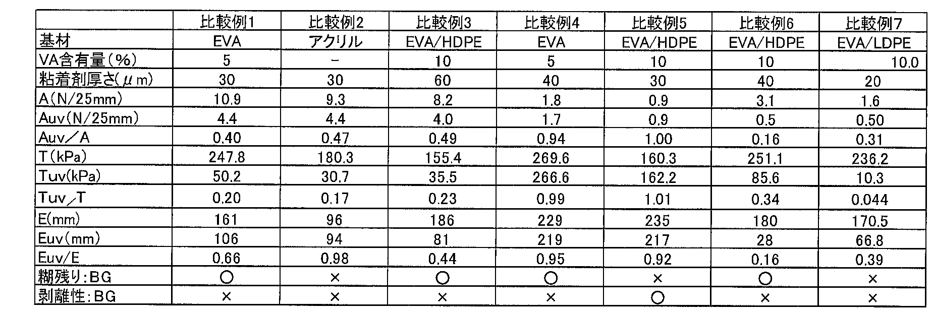
表1に示すように、実施例1~5は、AUV/A≦0.29と請求項1に規定のAUV/A≦0.3であり、かつTUV/T≦0.042と請求項1に規定のTUV/T≦0.05であり、EUV/E≦0.29と請求項1に規定のEUV/E≦0.3であるため、半導体ウェハ裏面の研削加工後に、糊残りなく容易に剥離することができた。
これに対して、比較例1~5は、AUV/Aが0.3より大きく、かつTUV/Tが0.05より大きく、かつEUV/Eが0.3より大きいため、糊残り及び/又は剥離性に劣る結果となった。また、TUV/Tが0.05より大きい比較例6、AUV/Aが0.3より大きい比較例7についても、糊残り及び/又は剥離性に劣る結果となった。
1:半導体ウェハ加工用粘着テープ
2:基材フィルム
3:粘着剤層
4:剥離フィルム
5:半導体ウェハ
7:研磨機
51:凹凸
2:基材フィルム
3:粘着剤層
4:剥離フィルム
5:半導体ウェハ
7:研磨機
51:凹凸
Claims (4)
- 基材フィルムと、前記基材フィルムの片面側に設けられたエネルギー線硬化型の粘着剤層とを有し、 エネルギー線照射前の粘着力をA(N/25mm)、タック力をT(KPa)、伸びをE(mm)とし、エネルギー線を照射した後の粘着力をAUV(N/25mm)、タック力をTUV(KPa)、伸びをEUV(mm)としたとき、AUV/A≦0.3であり、かつTUV/T≦0.05であり、かつEUV/E≦0.3であることを特徴とする半導体ウェハ加工用粘着テープ。
- 前記基材フィルムは、ポリエチレン及びエチレン共重合体から選ばれる少なくとも一つの樹脂からなる複数の樹脂層を含み、前記粘着剤層と接する前記樹脂層は、酢酸ビニル含有量が5~20質量%のエチレン酢酸ビニル共重合体からなり、前記粘着剤層と反対側の最も外側の樹脂層は、ポリエチレンまたは酢酸ビニル含有量が10質量%以下のエチレン酢酸ビニル共重合体からなることを特徴とする請求項1に記載の半導体ウェハ加工用粘着テープ。
- 前記粘着剤層は、厚さが20~40μmであり、エネルギー線反応性の離型剤を含むことを特徴とする請求項1または請求項2に記載の半導体ウェハ加工用粘着テープ。
- 表面に回路が形成された半導体ウェハの、裏面研削用であることを特徴とする請求項1から請求項3のいずれか一項に記載の半導体ウェハ加工用粘着テープ。
Priority Applications (2)
| Application Number | Priority Date | Filing Date | Title |
|---|---|---|---|
| CN201680005517.7A CN107112230A (zh) | 2015-03-16 | 2016-03-14 | 半导体晶圆加工用粘合带 |
| KR1020177019175A KR20170128210A (ko) | 2015-03-16 | 2016-03-14 | 반도체 웨이퍼 가공용 점착 테이프 |
Applications Claiming Priority (2)
| Application Number | Priority Date | Filing Date | Title |
|---|---|---|---|
| JP2015-051832 | 2015-03-16 | ||
| JP2015051832 | 2015-03-16 |
Publications (1)
| Publication Number | Publication Date |
|---|---|
| WO2016148110A1 true WO2016148110A1 (ja) | 2016-09-22 |
Family
ID=56919100
Family Applications (1)
| Application Number | Title | Priority Date | Filing Date |
|---|---|---|---|
| PCT/JP2016/058005 Ceased WO2016148110A1 (ja) | 2015-03-16 | 2016-03-14 | 半導体ウェハ加工用粘着テープ |
Country Status (3)
| Country | Link |
|---|---|
| KR (1) | KR20170128210A (ja) |
| CN (1) | CN107112230A (ja) |
| WO (1) | WO2016148110A1 (ja) |
Cited By (4)
| Publication number | Priority date | Publication date | Assignee | Title |
|---|---|---|---|---|
| CN109976384A (zh) * | 2019-03-13 | 2019-07-05 | 厦门理工学院 | 一种自治水下机器人及路径跟随控制方法、装置 |
| JPWO2021251422A1 (ja) * | 2020-06-10 | 2021-12-16 | ||
| JPWO2021251420A1 (ja) * | 2020-06-10 | 2021-12-16 | ||
| US11466184B2 (en) | 2018-06-20 | 2022-10-11 | Lg Chem, Ltd. | Adhesive composition |
Families Citing this family (1)
| Publication number | Priority date | Publication date | Assignee | Title |
|---|---|---|---|---|
| KR102677755B1 (ko) * | 2021-08-12 | 2024-06-24 | (주)이녹스첨단소재 | 웨이퍼 이면 연삭용 점착 필름 |
Citations (4)
| Publication number | Priority date | Publication date | Assignee | Title |
|---|---|---|---|---|
| JP2004186429A (ja) * | 2002-12-03 | 2004-07-02 | Furukawa Electric Co Ltd:The | 粘接着テープ |
| JP2006156754A (ja) * | 2004-11-30 | 2006-06-15 | Furukawa Electric Co Ltd:The | ダイシングダイボンドテープ |
| JP2007012670A (ja) * | 2005-06-28 | 2007-01-18 | Furukawa Electric Co Ltd:The | 粘接着テープ |
| JP2014015521A (ja) * | 2012-07-06 | 2014-01-30 | Furukawa Electric Co Ltd:The | 半導体ウェハ表面保護用粘着テープおよびそれを用いた半導体ウェハの製造方法 |
-
2016
- 2016-03-14 CN CN201680005517.7A patent/CN107112230A/zh active Pending
- 2016-03-14 KR KR1020177019175A patent/KR20170128210A/ko not_active Withdrawn
- 2016-03-14 WO PCT/JP2016/058005 patent/WO2016148110A1/ja not_active Ceased
Patent Citations (4)
| Publication number | Priority date | Publication date | Assignee | Title |
|---|---|---|---|---|
| JP2004186429A (ja) * | 2002-12-03 | 2004-07-02 | Furukawa Electric Co Ltd:The | 粘接着テープ |
| JP2006156754A (ja) * | 2004-11-30 | 2006-06-15 | Furukawa Electric Co Ltd:The | ダイシングダイボンドテープ |
| JP2007012670A (ja) * | 2005-06-28 | 2007-01-18 | Furukawa Electric Co Ltd:The | 粘接着テープ |
| JP2014015521A (ja) * | 2012-07-06 | 2014-01-30 | Furukawa Electric Co Ltd:The | 半導体ウェハ表面保護用粘着テープおよびそれを用いた半導体ウェハの製造方法 |
Cited By (7)
| Publication number | Priority date | Publication date | Assignee | Title |
|---|---|---|---|---|
| US11466184B2 (en) | 2018-06-20 | 2022-10-11 | Lg Chem, Ltd. | Adhesive composition |
| CN109976384A (zh) * | 2019-03-13 | 2019-07-05 | 厦门理工学院 | 一种自治水下机器人及路径跟随控制方法、装置 |
| CN109976384B (zh) * | 2019-03-13 | 2022-02-08 | 厦门理工学院 | 一种自治水下机器人及路径跟随控制方法、装置 |
| JPWO2021251422A1 (ja) * | 2020-06-10 | 2021-12-16 | ||
| JPWO2021251420A1 (ja) * | 2020-06-10 | 2021-12-16 | ||
| JP7440633B2 (ja) | 2020-06-10 | 2024-02-28 | 三井化学東セロ株式会社 | 電子装置の製造方法 |
| JP7440632B2 (ja) | 2020-06-10 | 2024-02-28 | 三井化学東セロ株式会社 | 電子装置の製造方法 |
Also Published As
| Publication number | Publication date |
|---|---|
| KR20170128210A (ko) | 2017-11-22 |
| CN107112230A (zh) | 2017-08-29 |
Similar Documents
| Publication | Publication Date | Title |
|---|---|---|
| JP5823591B1 (ja) | 半導体ウエハ表面保護用粘着テープおよび半導体ウエハの加工方法 | |
| JP7326270B2 (ja) | 半導体加工用粘着テープおよび半導体装置の製造方法 | |
| JP3383227B2 (ja) | 半導体ウエハの裏面研削方法 | |
| JP4851613B2 (ja) | 半導体ウエハ表面保護用粘着テープ | |
| JP5242830B1 (ja) | 半導体ウェハ表面保護用粘着テープおよび半導体ウェハの製造方法 | |
| JP6169067B2 (ja) | 電子部品加工用粘着テープ | |
| JP6306362B2 (ja) | 伸長可能シートおよび積層チップの製造方法 | |
| WO2017072901A1 (ja) | 半導体ウエハ表面保護用粘着テープおよび半導体ウエハの加工方法 | |
| CN107924864B (zh) | 半导体晶片半切割后的背面研削加工用紫外线硬化型粘合片 | |
| JP7339941B2 (ja) | 粘着テープおよび半導体装置の製造方法 | |
| JP6412873B2 (ja) | 粘着シート | |
| JP7353268B2 (ja) | 粘着テープおよび半導体装置の製造方法 | |
| JP5697061B1 (ja) | 半導体ウェハ加工用粘着テープおよび半導体ウェハの加工方法 | |
| WO2016148110A1 (ja) | 半導体ウェハ加工用粘着テープ | |
| JP2014192464A (ja) | 半導体ウェハ表面保護用粘着テープ | |
| WO2019181730A1 (ja) | 粘着テープおよび半導体装置の製造方法 | |
| KR20200024591A (ko) | 백 그라인딩 테이프 | |
| WO2011125683A1 (ja) | 半導体ウエハ加工用粘着シート | |
| JP2002203822A (ja) | 脆性部材の加工方法および両面粘着シート | |
| WO2018164175A1 (ja) | 半導体加工用粘着テープ | |
| TW202108392A (zh) | 電子零件用膠帶及電子零件之加工方法 | |
| JP4364368B2 (ja) | 半導体チップの製造方法 | |
| JP2009035717A (ja) | Uv硬化型粘着剤組成物及び半導体ウエハ加工用粘着テープ | |
| JP7069116B2 (ja) | バックグラインドテープ用基材 | |
| JP6800062B2 (ja) | 粘着テープ |
Legal Events
| Date | Code | Title | Description |
|---|---|---|---|
| 121 | Ep: the epo has been informed by wipo that ep was designated in this application |
Ref document number: 16764940 Country of ref document: EP Kind code of ref document: A1 |
|
| ENP | Entry into the national phase |
Ref document number: 20177019175 Country of ref document: KR Kind code of ref document: A |
|
| NENP | Non-entry into the national phase |
Ref country code: DE |
|
| 122 | Ep: pct application non-entry in european phase |
Ref document number: 16764940 Country of ref document: EP Kind code of ref document: A1 |