WO2016147951A1 - ナノファイバ製造装置、及び、ナノファイバ製造方法 - Google Patents
ナノファイバ製造装置、及び、ナノファイバ製造方法 Download PDFInfo
- Publication number
- WO2016147951A1 WO2016147951A1 PCT/JP2016/057149 JP2016057149W WO2016147951A1 WO 2016147951 A1 WO2016147951 A1 WO 2016147951A1 JP 2016057149 W JP2016057149 W JP 2016057149W WO 2016147951 A1 WO2016147951 A1 WO 2016147951A1
- Authority
- WO
- WIPO (PCT)
- Prior art keywords
- unit
- rotating body
- nanofibers
- deposited
- nanofiber manufacturing
- Prior art date
- Legal status (The legal status is an assumption and is not a legal conclusion. Google has not performed a legal analysis and makes no representation as to the accuracy of the status listed.)
- Ceased
Links
Images



Classifications
-
- D—TEXTILES; PAPER
- D01—NATURAL OR MAN-MADE THREADS OR FIBRES; SPINNING
- D01D—MECHANICAL METHODS OR APPARATUS IN THE MANUFACTURE OF ARTIFICIAL FILAMENTS, THREADS, FIBRES, BRISTLES OR RIBBONS
- D01D5/00—Formation of filaments, threads, or the like
- D01D5/04—Dry spinning methods
-
- D—TEXTILES; PAPER
- D01—NATURAL OR MAN-MADE THREADS OR FIBRES; SPINNING
- D01D—MECHANICAL METHODS OR APPARATUS IN THE MANUFACTURE OF ARTIFICIAL FILAMENTS, THREADS, FIBRES, BRISTLES OR RIBBONS
- D01D7/00—Collecting the newly-spun products
-
- D—TEXTILES; PAPER
- D04—BRAIDING; LACE-MAKING; KNITTING; TRIMMINGS; NON-WOVEN FABRICS
- D04H—MAKING TEXTILE FABRICS, e.g. FROM FIBRES OR FILAMENTARY MATERIAL; FABRICS MADE BY SUCH PROCESSES OR APPARATUS, e.g. FELTS, NON-WOVEN FABRICS; COTTON-WOOL; WADDING ; NON-WOVEN FABRICS FROM STAPLE FIBRES, FILAMENTS OR YARNS, BONDED WITH AT LEAST ONE WEB-LIKE MATERIAL DURING THEIR CONSOLIDATION
- D04H1/00—Non-woven fabrics formed wholly or mainly of staple fibres or like relatively short fibres
- D04H1/70—Non-woven fabrics formed wholly or mainly of staple fibres or like relatively short fibres characterised by the method of forming fleeces or layers, e.g. reorientation of fibres
- D04H1/72—Non-woven fabrics formed wholly or mainly of staple fibres or like relatively short fibres characterised by the method of forming fleeces or layers, e.g. reorientation of fibres the fibres being randomly arranged
- D04H1/728—Non-woven fabrics formed wholly or mainly of staple fibres or like relatively short fibres characterised by the method of forming fleeces or layers, e.g. reorientation of fibres the fibres being randomly arranged by electro-spinning
Definitions
- Embodiments described herein relate generally to a nanofiber manufacturing apparatus and a nanofiber manufacturing method.
- a nanofiber manufacturing device As a device for manufacturing a fiber material having a nano-unit diameter, a nanofiber manufacturing device is used in a wide field such as the medical field. Electrospinning technology is used in nanofiber manufacturing equipment.
- Electrospinning technology is a technology in which a raw material liquid in which a polymer substance or the like is dissolved and a work are charged, and the raw material liquid is discharged toward the work by a potential difference between the raw material liquid and the work. Nanofibers are manufactured by electrically stretching the raw material liquid. In such a nanofiber manufacturing apparatus, it is desired to improve productivity.
- Embodiments of the present invention provide a nanofiber manufacturing apparatus and a nanofiber manufacturing method with improved productivity.
- a nanofiber manufacturing apparatus including a collection unit, a discharge unit, a power supply unit, and a charge removal unit.
- the collection unit feeds the material to be deposited from one end and collects it at the other end.
- the material to be deposited has a first surface and a second surface opposite to the first surface.
- the discharge unit discharges a raw material liquid to deposit nanofibers on the first surface.
- the power supply unit generates a potential difference between the ejection unit and the first surface.
- the neutralization unit neutralizes charges charged in the deposited nanofibers.
- the material to be deposited is disposed between the discharge unit and the charge removal unit.
- the collection unit has at least a pair of first rotating bodies. The first rotating body causes the first surface to alternately face the discharge unit and the charge removal unit. A first direction in which the collecting unit sends the material to be deposited from one end is inclined with respect to a second direction from one side of the first rotating body to the other.
- FIG. 6A and FIG. 6B are schematic views showing a part of another nanofiber manufacturing apparatus according to this embodiment. It is a flowchart which shows the nanofiber manufacturing method which concerns on this embodiment.
- provided on includes not only the case of being provided in direct contact but also the case of being provided with another layer or film interposed therebetween.
- provided so as to face includes not only the case of being provided in direct contact with or above or below, but also the case of being provided with another layer or film interposed therebetween.
- FIG. 1 is a schematic diagram showing a nanofiber manufacturing apparatus according to this embodiment.
- FIG. 2 is a schematic diagram showing a part of the nanofiber manufacturing apparatus according to the present embodiment.
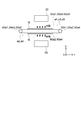
- FIG. 3 is a diagram for explaining film formation and charge removal by the nanofiber manufacturing apparatus according to the present embodiment.
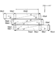
- FIG. 4 is a schematic view showing a part of another nanofiber manufacturing apparatus according to this embodiment.
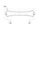
- FIG. 5 is a schematic diagram showing a part of the nanofiber manufacturing apparatus according to the present embodiment.
- FIG. 6A and FIG. 6B are schematic views showing a part of another nanofiber manufacturing apparatus according to this embodiment.
- FIG. 1 is a perspective view of the nanofiber manufacturing apparatus 100.
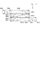
- 2 and 4 are front views of the collection unit 50 as viewed from the ejection direction of the ejection unit 30.
- FIG. FIG. 3 is a side view of the nanofiber manufacturing apparatus 100. 5, 6 (a), and 6 (b) show a part of the collection unit 50.
- the nanofiber manufacturing apparatus 100 includes a power supply unit 10, a control unit 20, a discharge unit 30, a charge removal unit 40, and a collection unit 50.
- the collecting unit 50 is provided with a base material 60 on which the nanofibers N are deposited.
- the direction of arrow A1 in FIG. 1 indicates the direction in which the discharge unit 30 discharges the raw material liquid.
- the directions of the plurality of arrows A2 indicate directions (conveyance directions) in which the base material 60 is moved and conveyed by the movement of the collecting unit 50.
- the substrate 60 has a first surface 60a and a second surface 60b.
- the second surface 60b is a surface opposite to the first surface 60a.
- a direction perpendicular to the first surface 60a is taken as a Z-axis direction.
- One direction perpendicular to the Z-axis direction is taken as an X-axis direction.
- a direction perpendicular to the Z-axis direction and the X-axis direction is taken as a Y-axis direction.
- the first surface 60a is parallel to the XY plane.
- the raw material liquid remaining at the tip of the discharge unit 30 due to surface tension is positive (or negative). Is charged. Further, the raw material liquid is attracted by the electrostatic force acting along the lines of electric force directed to the collecting unit 50 that is charged (or grounded) to a different polarity. Note that the voltage applied between the ejection unit 30 and the collection unit 50 is about 10 to 100 kV.
- the raw material liquid is discharged from the tip portion of the discharge unit 30.
- the raw material liquid discharged from the tip portion is discharged toward the first surface 60 a of the base material 60 provided in the collecting unit 50.
- the solvent contained in the raw material liquid is volatilized, and the polymer fibrous body reaches the first surface 60 a of the substrate 60.
- the nanofibers N are deposited on the first surface 60a of the substrate 60.
- the nanofiber N represented by the hatched portion is deposited on the first surface 60 a of the substrate 60.
- the nanofiber manufacturing apparatus 100 of this embodiment forms the nanofiber N using an electrospinning method.
- the nanofiber N having a shape such as a smooth surface, a porous surface, a bead shape, a core-sheath shape, a hollow shape, or an ultrafine fiber is deposited on the first surface 60 a of the base material 60 by the nanofiber manufacturing apparatus 100.
- the power supply unit 10 is a power supply device that applies a high voltage between the discharge unit 30 and the collection unit 50.
- the power supply unit 10 is a power supply device using a DC power supply, for example.
- one terminal of the power supply unit 10 is electrically connected to the discharge unit 30, and the other terminal of the power supply unit 10 is grounded.
- One end of the collecting unit 50 is grounded. Such a connection can generate a potential difference between the ejection unit 30 and the collection unit 50.
- the control unit 20 is, for example, a computer including a CPU (Central Processing Unit) and a memory.
- the control unit 20 controls operations of the power supply unit 10 and the discharge unit 30.
- the control unit 20 is electrically connected to the power supply unit 10 and the discharge unit 30.
- the control unit 20 controls the power supply unit 10 so as to determine the voltage value applied to the ejection unit 30.
- the control unit 20 controls the discharge unit 30 so as to determine the amount of discharge liquid.
- the control unit 20 determines the voltage value of the power supply unit 10 and the discharge amount of the discharge unit 30, and then determines the position of the discharge unit 30 relative to the base material 60. For example, the control unit 20 drives a driving device or the like to move the discharge unit 30 in the X-axis direction, the Y-axis direction, and the Z-axis direction. Thereby, the position (discharge position) with respect to the base material 60 of the discharge part 30 is determined. After determining the position of the discharge unit 30 with respect to the base material 60, the control unit 20 controls the power supply unit 10 and the discharge unit 30 to determine the voltage value of the power supply unit 10 and the discharge amount of the discharge unit 30, respectively. May be.
- control unit 20 can be electrically connected to the static elimination unit 40 and the collection unit 50 to control the operations of the static elimination unit 40 and the collection unit 50.
- control unit 20 is electrically connected to the charge removal unit 40 and the collection unit 50, and controls the charge removal operation of the charge removal unit 40 and the drive (for example, rotational drive) of the collection unit 50.
- the discharge part 30 is provided facing the base material 60, for example.
- the discharge unit 30 is, for example, a nozzle that discharges a raw material liquid that is a material for forming the nanofibers N.
- the raw material liquid is stored in a tank or the like provided separately from the discharge unit 30 and supplied from the tank to the discharge unit 30 via a pipe.
- the raw material liquid stored in the discharge unit 30 is discharged from the tip portion.
- the discharge unit 30 performs discharge processing from the first surface 60a side of the substrate 60 to deposit the nanofibers N on the first surface 60a.
- the raw material liquid is a liquid in which a solute that is a material of the nanofiber N is dispersed or dissolved in a solvent.
- the raw material liquid is a liquid that is appropriately adjusted depending on the material of the nanofiber N, the nature of the nanofiber N, and the like.
- a resin is a solute that is dispersed or dissolved in a raw material liquid.
- a solvent used for the raw material liquid there is a volatile organic solvent.
- An inorganic solid material may be added to the raw material liquid.
- the static eliminating unit 40 is, for example, an electrostatic removal device (ionizer) such as an ion generator.
- ionizer electrostatic removal device
- the nanofibers N deposited on the substrate 60 have a positive charge.
- the positively charged nanofibers N repel each other, it is difficult to continuously deposit the nanofibers N. Therefore, by using a negative ion generator in the static elimination unit 40, the nanofibers N can be continuously deposited on the substrate 60 by eliminating (neutralizing) the positive charges of the nanofibers N that have already been deposited. it can.
- the static elimination part 40 is provided substantially perpendicularly with respect to the longitudinal direction of the base material 60, for example.
- the static elimination part 40 is provided substantially perpendicularly with respect to the conveyance direction of the base material 60, for example.
- the static eliminator 40 is provided substantially perpendicular to the conveyance direction of the base material 60, when the base material 60 is conveyed by driving the collection unit 50, the static eliminator 40 is applied to the nanofibers N deposited on the base material 60. Thus, it is possible to carry out static elimination processing continuously.
- the static elimination part 40 is provided facing the base material 60 on the opposite side to the side where the base material 60 opposes the discharge part 30, for example. That is, the base material 60 is disposed between the discharge unit 30 and the charge removal unit 40.
- the nanofiber N deposited on the first surface 60a is moved by driving the collecting unit 50, the charge of the nanofiber N deposited on the first surface 60a can be removed.
- the nanofibers N deposited on the first surface 60 a move again by driving the collection unit 50.
- the nanofibers N are deposited again on the first surface 60 a by the discharge unit 30.
- the charge removal unit 40 performs the charge removal process on the nanofibers N deposited on the first surface 60 a by the discharge unit 30.
- the collecting unit 50 has a plurality of rotating bodies 50A.
- the rotating body 50A is a rotating roller.
- the rotating body 50A is provided with a rotating shaft, and the rotating shaft is rotated by the control of the control unit 20, for example. By such rotational driving of the rotating body 50A, the collecting unit 50 is driven and the substrate 60 is conveyed.
- the plurality of rotating bodies 50A can be configured by the first rotating body 50a, the second rotating body 50b, and the third rotating body 50c. Since the base member 60 is transported by the first rotating body 50a, the discharging process (deposition of the nanofibers N) by the discharging unit 30 and the discharging process by the discharging unit 40 can be alternately repeated.
- the first rotating body 50a is provided between the second rotating bodies 50b and between the third rotating bodies 50c in the conveyance direction of the base material 60 (the direction of the plurality of arrows A2 in FIG. 1).
- the base member 60 can be transported in the transport direction by the second rotating body 50b.
- the second rotating body 50b is provided between the third rotating bodies 50c in the conveyance direction of the base material 60.
- the third rotating body 50c is a rotating body that feeds the substrate 60 from one end of the collecting unit 50 and collects it at the other end.
- the third rotating body 50 c is, for example, a rotating body for unwinding the base material 60 or a rotating body for winding the base material 60.
- the base member 60 is unwound by the third rotating body 50c, and the discharge process (deposition of the nanofibers N) by the discharge unit 30 and the discharge process by the charge removal unit 40 are alternately repeated to deposit the nanofibers N.
- the base material 60 thus wound is wound up.
- the base material 60 is, for example, a sheet-like member.
- the rotating body 50A is a rotating roller and the substrate 60 is a sheet-like member, a part of the sheet-like member is wound around the rotating roller.
- the rotating roller rotates under the control of the control unit 20 and conveys the sheet-like member in the conveying direction.
- the collection unit 50 includes four first rotating bodies 50a1 to 50a4, two second rotating bodies 50b1 and 50b2, and two third rotating bodies 50c1 and 50c2.
- Surfaces 60 a 1, 60 a 3, and 60 a 5 that are the first surface 60 a of the base material 60 and are subjected to ejection processing (deposition of nanofibers N) by the ejection unit 30 are represented by solid line portions.
- surfaces 60a2 and 60a4 that are the first surface 60a of the base member 60 and are subjected to the charge removal process by the charge removal unit 40 are represented by broken line portions. That is, all of the surfaces 60a1 to 60a6 correspond to surfaces on which the first surface 60a of the substrate 60 is conveyed.
- the directions of arrows a1 to a6 (hereinafter sometimes referred to as directions d1 to d6) correspond to the directions of the plurality of arrows A2 in FIG.
- the base material 60 is unwound from the third rotating body 50c1 and conveyed to the surface 60a1.
- the conveyance direction of the base material 60 is the direction d1.
- the base material 60 is conveyed to the surface 60a1 by the rotational driving of the second rotating body 50b1 and the third rotating body 50c1.
- the nanofibers N are deposited on the surface 60a1 by the discharge process of the discharge unit 30 at the processing time t2.
- the nanofibers N deposited at the processing time t2 are conveyed to the surface 60a2.
- the conveyance direction of the base material 60 is the direction d2.
- the nanofibers N deposited at the processing time t2 are conveyed from the surface 60a1 to the surface 60a2 by the rotational driving of the first rotating body 50a1.
- the charge of the nanofibers N transferred to the surface 60 a 2 by the charge removal process of the charge removal unit 40 is discharged at the processing time t ⁇ b> 4.
- the nanofiber N that has been neutralized at the processing time t4 is conveyed to the surface 60a3.
- the conveyance direction of the base material 60 is the direction d3.
- the nanofiber N that has been neutralized at the processing time t4 is conveyed from the surface 60a2 to the surface 60a3 by the rotational drive of the first rotating body 50a2.
- the nanofibers N are deposited again on the surface 60a3 by the discharge process of the discharge unit 30.
- the nanofibers N deposited again at the processing time t6 are transported to the surface 60a4.
- the conveyance direction of the base material 60 is the direction d4.
- the nanofibers N deposited again at the processing time t6 are transported from the surface 60a3 to the surface 60a4 by the rotational driving of the first rotating body 50a3.
- the charge of the nanofiber N transferred to the surface 60 a 4 by the charge removal process of the charge removal unit 40 is discharged at the processing time t ⁇ b> 8.
- the nanofiber N that has been neutralized at the processing time t8 is conveyed to the surface 60a5.
- the conveyance direction of the base material 60 is the direction d5.
- the nanofiber N that has been neutralized at the processing time t8 is conveyed from the surface 60a4 to the surface 60a5 by the rotational drive of the first rotating body 50a4.
- the nanofibers N are deposited again on the surface 60a5 by the discharge process of the discharge unit 30 at the processing time t10.
- the substrate 60 is conveyed from the surface 60a5 and wound around the third rotating body 50c2.
- the conveyance direction of the base material 60 is the direction d6.
- the base material 60 is wound around the third rotating body 50c2 by the rotational driving of the second rotating body 50b2 and the third rotating body 50c2.
- the deposition of the nanofibers N by the discharge unit 30 and the charge removal of the deposited nanofibers N by the discharging unit 40 are alternately performed from the processing time t2 to the processing time t10. .
- the nanofiber N can be deposited efficiently.
- a thick nanofiber N can be continuously deposited.
- the rotating body 50A includes four first rotating bodies 50a1 to 50a4, two second rotating bodies 50b1 and 50b2, and two third rotating bodies 50c1 and 50c2.
- the rotating body 50A may be configured by two first rotating bodies 50a, two second rotating bodies 50b, and two third rotating bodies 50c.
- the rotating body 50A may be configured by six first rotating bodies 50a, two second rotating bodies 50b, and two third rotating bodies 50c. That is, at least a pair of first rotating bodies 50 a can be provided in the collecting unit 50.
- the number and arrangement of the second rotating bodies 50b are arbitrary, and the second rotating body 50b may not be provided as long as the substrate 60 can be conveyed to the first rotating body 50a.
- first rotating body 50a and the second rotating body 50b are arranged in parallel in the X-axis direction.
- the X-axis direction corresponds to the third direction.
- the arrangement direction of the first rotating body 50a and the second rotating body 50b is not limited to this.
- the number of the first rotating bodies 50a When the number of the first rotating bodies 50a is increased, the number of times of reciprocating the substrate 60 can be increased. For example, if the number of times of reciprocating the base material 60 is increased, the film thickness of the nanofibers N deposited on the base material 60 can be increased. Based on the number of first rotating bodies 50a, the film thickness of the nanofibers N deposited on the substrate 60 can be controlled. The film thickness of the nanofibers N deposited on the substrate 60 can also be controlled by the speed at which the substrate 60 is conveyed.
- the surface 60a2 is provided with an angle ⁇ inclined with respect to the surfaces 60a1 and 60a3, and the surface 60a4 is provided with an angle ⁇ inclined with respect to the surfaces 60a3 and 60a5. That is, the first rotating bodies 50a1 to 50a4 are provided with an angle ⁇ inclined with respect to the second rotating bodies 50b1 and 50b2. For example, when the second rotating bodies 50b1 and 50b2 are provided in parallel with the X-axis direction, the first rotating bodies 50a1 to 50a4 are provided with an angle ⁇ inclined with respect to the X-axis direction.
- the direction d2 is a direction inclined by a predetermined angle ⁇ with respect to the directions d1 and d3, and the direction d4 is a direction inclined by a predetermined angle ⁇ with respect to the directions d3 and d5.
- the directions d1, d3, and d5 are ⁇ Y axis directions
- the directions d2 and d4 are directions inclined by a predetermined angle ⁇ with respect to the ⁇ Y axis direction.
- the directions d1, d3, and d5 are set as the first direction
- the direction d2 is the second direction, and the first rotating body 50a1 to the first rotating body 50a2 in the pair of first rotating bodies 50a1 and 50a2 facing each other.
- the direction d4 is the second direction, and is a direction from the first rotating body 50a3 toward the first rotating body 50a4 in the pair of first rotating bodies 50a3 and 50a4 facing each other. With such an angle ⁇ , the substrate 60 can be transported in a spiral shape.
- the angle ⁇ is an arbitrary value.
- the first rotating bodies 50a1 to 50a4 are provided at an angle ⁇ with respect to the second rotating bodies 50b1 and 50b2, and the first rotating bodies 50a1 to 50a4 and the first rotating bodies 50a1 to 50a4 and the length of the base member 60 in the discharge process are changed.
- the second rotating bodies 50b1 and 50b2 can be arranged. For example, as shown in FIG. 4, by providing the base material 60 having the lengths L1 and L2, the area of the surface 60a3 can be made larger than the areas of the surfaces 60a1 and 60a1 to be discharged.
- the shape of the rotating body 50A is an arbitrary shape.
- the rotating body 50A has a shape as shown in FIG. 5, when the rotating body 50A is driven to rotate, a force that is pulled to an end portion having a large roll diameter works. That is, force is applied to the rotating body 50A in the directions of the arrows A3 and A4.
- the rotating body 50A has a shape in which the roll diameter at one end is larger than the roll diameter at the other end as shown in FIGS. 6 (a) and 6 (b)
- the rotating body 50A is moved from one end to the other end. It has a shape in which the cross-sectional dimension increases as it goes.
- a force acts in the direction of arrow A5 depending on the angle ⁇ , and at the end portion with a large roll diameter, a force acts in the direction of arrow A6 due to a peripheral speed difference generated from the difference in roll diameter.
- the surface 60a2 is provided at an angle ⁇ with respect to the surfaces 60a1 and 60a3, and the surface 60a4 is provided at an angle ⁇ with respect to the surfaces 60a3 and 60a5.
- the rotating body 50A has a shape as shown in FIG. 6A, the base material 60 can be stably conveyed while suppressing the sagging of the base material 60.
- the deposited nanofibers are positively charged and the nanofibers repel each other.
- the discharge process and the charge removal process are alternately installed on the production line, the production line becomes long.
- the manufacturing cost increases.
- a collection unit 50 having at least a pair of first rotating bodies 50a is provided.
- the first rotating body 50a is provided with a predetermined angle inclination, and the first surface 60a of the base 60 is moved from one of the discharge unit 30 and the charge removing unit 40 to the other by the rotation of the first rotating body 50a. opposite.
- the discharge process (deposition of nanofibers N) by the discharge unit 30 and the charge removal process by the charge removal unit 40 can be alternately repeated. Thereby, the space of discharge processing and static elimination processing can be reduced.
- the discharge process and the charge removal process can be performed with a small number of discharge apparatuses and charge removal apparatuses, the manufacturing cost can be reduced.
- the processing time can be shortened.
- a nanofiber manufacturing apparatus with improved productivity can be provided.
- FIG. 7 is a flowchart showing the nanofiber manufacturing method according to this embodiment.
- the base material 60 is unwound, and the first surface 60a of the base material 60 is opposed to the discharge unit 30 (step S110).
- the base 60 is unwound from the third rotating body 50c, and the first surface 60a is opposed to the discharge unit 30 by driving the discharge unit 30 in the X-axis direction, the Y-axis direction, and the Z-axis direction.
- the nanofiber N is deposited on the 1st surface 60a by the discharge process of the discharge part 30 (step S120).
- the first surface 60a on which the nanofibers N are deposited is conveyed, and the first surface 60a is opposed to the charge removal unit 40 (step S130).
- the first surface 60a on which the nanofibers N are deposited is opposed to the charge removal unit 40 by the rotational drive of the first rotating body 50a.
- step S140 The charge of the nanofiber N deposited on the first surface 60a by the charge removal process of the charge removal unit 40 is removed.
- the first surface 60a provided with the removed nanofibers N is conveyed, and the first surface 60a is again opposed to the ejection unit 30 (step S150).
- the first surface 60a on which the removed nanofibers N are provided is opposed to the ejection unit 30 again by the rotational driving of the first rotating body 50a.
- the nanofibers N are deposited again on the first surface 60a provided with the nanofibers N by the discharge process of the discharge unit 30 (step S160).
- steps S130 to S160 are repeated until the nanofiber N has a desired film thickness.
- steps S130 to S160 are repeated until the set number of times.
- Steps S130 to S160 are repeated up to the determined number. Steps S130 to S160 are repeated until such conditions (desired film thickness, number of ejection processes, etc.) are satisfied.
- a nanofiber manufacturing method with improved productivity can be provided.
- a program (for example, a program for executing the processing of FIG. 7) that operates the configuration of the above-described embodiment so as to realize the function of the above-described embodiment is stored in a storage medium, and the program stored in the storage medium is used as a code Processing methods that are read out and executed in a computer are also included in the category of the above-described embodiment.
- a computer-readable recording medium is included in the scope of the present embodiment.
- the storage medium storing the above-described computer program is also included in the above-described embodiment.
- a floppy (registered trademark) disk for example, a hard disk, an optical disk, a magneto-optical disk, a CD-ROM, a magnetic tape, a nonvolatile memory card, a ROM, or the like can be used.
- a nanofiber manufacturing apparatus and a nanofiber manufacturing method with improved productivity are provided.
Landscapes
- Engineering & Computer Science (AREA)
- Textile Engineering (AREA)
- Mechanical Engineering (AREA)
- Spinning Methods And Devices For Manufacturing Artificial Fibers (AREA)
- Nonwoven Fabrics (AREA)
Abstract
収集部(50)と、吐出部(30)と、電源部(10)と、除電部(40)と、を備えたナノファイバ製造装置(100)が提供される。前記収集部(50)は、被堆積材(60)を一端から送り出して他端で収集する。前記被堆積材(60)は、第1面(60a)と、前記第1面(60a)と反対の第2面(60b)と、を有する。前記吐出部(30)は、原料液を吐出して前記第1面(60a)にナノファイバ(N)を堆積させる。前記電源部(10)は、前記吐出部(30)と、前記第1面(60a)と、の間に電位差を発生させる。前記除電部(40)は、堆積した前記ナノファイバ(N)に帯電した電荷を除電する。前記被堆積材(60)は、前記吐出部(30)と、前記除電部(40)と、の間に配置される。前記収集部(50)は、少なくとも一対の第1回転体を有する。前記第1回転体は、前記第1面(60a)を前記吐出部(30)及び前記除電部(40)に交互に対向させる。前記収集部(50)が前記被堆積材(60)を一端から送り出す第1方向は、前記第1回転体の一方から他方に向かう第2方向に対して傾斜している。
Description
本発明の実施形態は、ナノファイバ製造装置、及び、ナノファイバ製造方法に関する。
ナノ単位の直径を有する繊維物質を製造する装置として、ナノファイバ製造装置が医療分野等の広い分野に用いられている。ナノファイバ製造装置において、エレクトロスピニング技術が用いられている。
エレクトロスピニング技術とは、高分子物質等が溶解した原料液と、ワークと、を帯電させ、原料液及びワークの電位差によって原料液をワークに向かって吐出させる技術である。原料液が電気的に延伸することでナノファイバが製造される。このようなナノファイバ製造装置において、生産性を向上させることが望まれる。
本発明の実施形態は、より生産性が向上したナノファイバ製造装置及びナノファイバ製造方法を提供する。
本発明の実施形態によれば、収集部と、吐出部と、電源部と、除電部と、備えたナノファイバ製造装置が提供される。前記収集部は、被堆積材を一端から送り出して他端で収集する。前記被堆積材は、第1面と、前記第1面と反対の第2面と、を有する。前記吐出部は、原料液を吐出して前記第1面にナノファイバを堆積させる。前記電源部は、前記吐出部と、前記第1面と、の間に電位差を発生させる。前記除電部は、堆積した前記ナノファイバに帯電した電荷を除電する。前記被堆積材は、前記吐出部と、前記除電部と、の間に配置される。前記収集部は、少なくとも一対の第1回転体を有する。前記第1回転体は、前記第1面を前記吐出部及び前記除電部に交互に対向させる。前記収集部が前記被堆積材を一端から送り出す第1方向は、前記第1回転体の一方から他方に向かう第2方向に対して傾斜している。
以下に、本発明の各実施の形態について図面を参照しつつ説明する。
なお、図面は模式的または概念的なものであり、各部分の厚みと幅との関係、部分間の大きさの比率などは、必ずしも現実のものと同一とは限らない。また、同じ部分を表す場合であっても、図面により互いの寸法や比率が異なって表される場合もある。
なお、本願明細書と各図において、既出の図に関して前述したものと同様の要素には同一の符号を付して詳細な説明は適宜省略する。
なお、図面は模式的または概念的なものであり、各部分の厚みと幅との関係、部分間の大きさの比率などは、必ずしも現実のものと同一とは限らない。また、同じ部分を表す場合であっても、図面により互いの寸法や比率が異なって表される場合もある。
なお、本願明細書と各図において、既出の図に関して前述したものと同様の要素には同一の符号を付して詳細な説明は適宜省略する。
本願明細書において、「上に設けられる」とは、直接接して設けられる場合の他に、間に他の層又は膜が挿入されて設けられる場合も含む。また、「対向して設けられる」とは、上または下に直接接してもしくは離間して設けられる場合の他に、間に他の層又は膜が挿入されて設けられる場合も含む。
(本実施形態)
図1は、本実施形態に係るナノファイバ製造装置を示す模式図である。
図2は、本実施形態に係るナノファイバ製造装置の一部を示す模式図である。
図3は、本実施形態に係るナノファイバ製造装置による成膜及び除電を説明する図である。
図4は、本実施形態に係る別のナノファイバ製造装置の一部を示す模式図である。
図5は、本実施形態に係るナノファイバ製造装置の一部を示す模式図である。
図6(a)及び図6(b)は、本実施形態に係る別のナノファイバ製造装置の一部を示す模式図である。
図1は、本実施形態に係るナノファイバ製造装置を示す模式図である。
図2は、本実施形態に係るナノファイバ製造装置の一部を示す模式図である。
図3は、本実施形態に係るナノファイバ製造装置による成膜及び除電を説明する図である。
図4は、本実施形態に係る別のナノファイバ製造装置の一部を示す模式図である。
図5は、本実施形態に係るナノファイバ製造装置の一部を示す模式図である。
図6(a)及び図6(b)は、本実施形態に係る別のナノファイバ製造装置の一部を示す模式図である。
図1は、ナノファイバ製造装置100の斜視図である。図2及び図4は、吐出部30の吐出方向から見た収集部50の正面図である。図3は、ナノファイバ製造装置100の側面図である。図5、図6(a)及び図6(b)は、収集部50の一部を示している。
図1に表すように、ナノファイバ製造装置100は、電源部10と、制御部20と、吐出部30と、除電部40と、収集部50と、を備える。収集部50には、ナノファイバNを堆積させる基材60が設けられている。図1の矢印A1の方向は、吐出部30が原料液を吐出する方向を示している。また、複数の矢印A2の方向は、収集部50の可動によって基材60が可動して搬送される方向(搬送方向)を示している。
基材60は、第1面60a及び第2面60bを有する。第2面60bは、第1面60aに反対側の面である。また、第1面60aに対して垂直な方向をZ軸方向とする。Z軸方向に対して垂直な1つの方向をX軸方向とする。Z軸方向とX軸方向とに対して垂直な方向をY軸方向とする。第1面60aは、X-Y平面に対して平行である。
本実施形態のナノファイバ製造装置100において、吐出部30と、収集部50と、の間に電圧を印加すると、表面張力によって吐出部30の先端部分に留まっている原料液は正(または負)に帯電する。また、原料液は、異極に帯電(またはアース)している収集部50に向かう電気力線に沿って作用する静電力によって吸引される。なお、吐出部30と、収集部50と、の間に印加する電圧は、10~100kV程度である。
静電力が表面張力より大きくなると、原料液が吐出部30の先端部分から吐出される。先端部分から吐出された原料液は、収集部50に設けられた基材60の第1面60aに向かって吐出される。このとき、原料液に含まれる溶媒は揮発し、ポリマーの繊維体が基材60の第1面60aに到達する。これにより、ナノファイバNが基材60の第1面60aに堆積される。例えば、斜線部分で表されたナノファイバNが基材60の第1面60aに堆積される。本実施形態のナノファイバ製造装置100は、エレクトロスピニング法を用いてナノファイバNを形成する。
ナノファイバ製造装置100によって、平滑表面、多孔表面、ビーズ状、芯鞘状、中空状、極細ファイバー等の形状を有するナノファイバNが基材60の第1面60aに堆積される。
電源部10は、吐出部30と、収集部50と、の間に高電圧を印加する電源装置である。電源部10は、例えば、直流電源を用いた電源装置である。例えば、電源部10の一方の端子は、吐出部30に電気的に接続され、電源部10の他方の端子は、接地されている。また、収集部50の一端は、接地されている。このような接続によって、吐出部30と、収集部50と、の間に電位差を発生させることができる。
制御部20は、例えば、CPU(Central Processing Unit)及びメモリー等を備えたコンピュータである。制御部20は、電源部10及び吐出部30の動作を制御する。制御部20は、電源部10及び吐出部30に電気的に接続されている。制御部20は、吐出部30に印加される電圧値を決定するように電源部10を制御する。制御部20は、吐出液の量を決定するように吐出部30を制御する。
制御部20は、電源部10の電圧値、及び、吐出部30の吐出量を決定した後、吐出部30の基材60に対する位置を決定する。制御部20は、例えば、駆動装置等を駆動させて吐出部30をX軸方向、Y軸方向及びZ軸方向に移動させる。これにより、吐出部30の基材60に対する位置(吐出位置)を決定する。制御部20は、吐出部30の基材60に対する位置を決定した後、電源部10の電圧値、及び、吐出部30の吐出量を決定するように電源部10及び吐出部30をそれぞれ制御しても良い。
また、制御部20は、除電部40及び収集部50に電気的に接続して除電部40及び収集部50の動作を制御することができる。このような場合、例えば、制御部20は、除電部40及び収集部50に電気的に接続され、除電部40の除電動作、及び、収集部50の駆動(例えば、回転駆動)を制御する。
吐出部30は、例えば、基材60に対向して設けられている。吐出部30は、例えば、ナノファイバNを形成する材料である原料液を吐出するノズルである。例えば、原料液は、吐出部30とは別に設けられたタンク等に蓄えられ、タンクからパイプを介して吐出部30に供給される。吐出部30に蓄えられた原料液は、先端部分から吐出される。吐出部30は、基材60の第1面60a側から吐出処理を行って第1面60aにナノファイバNを堆積させる。
原料液は、ナノファイバNの材料となる溶質を溶媒中に分散または溶解させた液体である。また、原料液は、ナノファイバNの材質やナノファイバNの性質等により適宜調整される液体である。例えば、原料液に分散または溶解する溶質として樹脂がある。また、原料液に使用される溶媒としては、揮発性のある有機溶剤がある。原料液に無機質固体材料を添加しても良い。
除電部40は、例えば、イオン発生器等の静電除去装置(イオナイザ)である。例えば、吐出部30の先端部分が正に帯電している場合、基材60の上に堆積されたナノファイバNは正電荷を有する。このような場合、正に帯電したナノファイバN同士は反発するのでナノファイバNを連続して堆積し難い。したがって、除電部40にマイナスイオン発生器を用いて、既に堆積したナノファイバNの正電荷を除電(中和)することにより、基材60の上にナノファイバNを連続して堆積することができる。
除電部40は、例えば、基材60の長手方向に対して略垂直に設けられている。除電部40は、例えば、基材60の搬送方向に対して略垂直に設けられている。基材60の搬送方向に対して略垂直に除電部40を設けると、基材60が収集部50の駆動によって搬送される場合、除電部40は、基材60に堆積したナノファイバNに対して連続的に除電処理を行うことができる。
除電部40は、例えば、基材60が吐出部30に対向する側と反対側において、基材60に対向して設けられている。つまり、基材60は、吐出部30と、除電部40と、の間に配置されている。これにより、第1面60aに堆積されたナノファイバNが収集部50の駆動によって移動した場合、第1面60aに堆積されたナノファイバNの電荷を除電することができる。除電部40による除電処理後、第1面60aに堆積されたナノファイバNは、収集部50の駆動によって再度移動する。そして、吐出部30によって第1面60aにナノファイバNを再度堆積させる。このように、除電部40は、吐出部30によって第1面60aに堆積されたナノファイバNに除電処理を行う。
収集部50は、複数の回転体50Aを有する。例えば、回転体50Aは、回転ローラである。回転体50Aには回転軸が設けられ、例えば、制御部20の制御によって回転軸が回転する。このような回転体50Aの回転駆動によって、収集部50の駆動が行われて基材60が搬送される。
また、複数の回転体50Aは、第1回転体50aと、第2回転体50bと、第3回転体50cと、によって構成することができる。
第1回転体50aによって基材60が搬送されるので、吐出部30による吐出処理(ナノファイバNの堆積)と、除電部40による除電処理と、を交互に繰り返すことができる。第1回転体50aは、例えば、基材60の搬送方向(図1の複数の矢印A2の方向)において、第2回転体50b間、及び、第3回転体50c間に設けられている。
第1回転体50aによって基材60が搬送されるので、吐出部30による吐出処理(ナノファイバNの堆積)と、除電部40による除電処理と、を交互に繰り返すことができる。第1回転体50aは、例えば、基材60の搬送方向(図1の複数の矢印A2の方向)において、第2回転体50b間、及び、第3回転体50c間に設けられている。
第2回転体50bによって、基材60を搬送方向に搬送することができる。第2回転体50bは、例えば、基材60の搬送方向において、第3回転体50c間に設けられている。
第3回転体50cは、基材60を収集部50の一端から送り出して他端で収集する回転体である。第3回転体50cは、例えば、基材60を巻き出すための回転体、又は、基材60を巻き取るための回転体である。第3回転体50cによって、基材60が巻き出されて、吐出部30による吐出処理(ナノファイバNの堆積)と、除電部40による除電処理と、を交互に繰り返されてナノファイバNが堆積した基材60が巻き取られる。
基材60は、例えば、シート状の部材である。回転体50Aが回転ローラであって、基材60がシート状の部材である場合、シート状の部材の一部が回転ローラに巻き付いている。回転ローラは、制御部20の制御によって回転してシート状の部材を搬送方向に搬送する。
以下、処理時間t1から処理時間t11に、基材60にナノファイバNを堆積させ、収集部50によって基材60を搬送する処理を説明する。
説明の便宜上、収集部50は、4つの第1回転体50a1~50a4と、2つの第2回転体50b1、50b2と、2つの第3回転体50c1、50c2と、を有するものとする。基材60の第1面60aであって、吐出部30によって吐出処理(ナノファイバNの堆積)される面60a1、60a3、60a5は、実線部分で表すものとする。また、基材60の第1面60aであって、除電部40によって除電処理される面60a2、60a4は、破線部分で表すものとする。つまり、面60a1~面60a6のいずれも、基材60の第1面60aが搬送される面に相当する。また、矢印a1~a6の方向(以下、方向d1~d6と呼ぶ場合がある。)は、図1の複数の矢印A2の方向に対応し、搬送方向を示すものとする。
説明の便宜上、収集部50は、4つの第1回転体50a1~50a4と、2つの第2回転体50b1、50b2と、2つの第3回転体50c1、50c2と、を有するものとする。基材60の第1面60aであって、吐出部30によって吐出処理(ナノファイバNの堆積)される面60a1、60a3、60a5は、実線部分で表すものとする。また、基材60の第1面60aであって、除電部40によって除電処理される面60a2、60a4は、破線部分で表すものとする。つまり、面60a1~面60a6のいずれも、基材60の第1面60aが搬送される面に相当する。また、矢印a1~a6の方向(以下、方向d1~d6と呼ぶ場合がある。)は、図1の複数の矢印A2の方向に対応し、搬送方向を示すものとする。
図2に表すように、処理時間t1に、基材60が第3回転体50c1から巻き出されて面60a1に搬送される。基材60の搬送方向は、方向d1である。基材60は、第2回転体50b1及び第3回転体50c1の回転駆動によって面60a1に搬送される。そして、図3に表すように、処理時間t2に、吐出部30の吐出処理によって面60a1にナノファイバNを堆積させる。
図2に表すように、処理時間t3に、処理時間t2に堆積したナノファイバNを面60a2に搬送させる。基材60の搬送方向は、方向d2である。処理時間t2に堆積したナノファイバNは、第1回転体50a1の回転駆動によって面60a1から面60a2に搬送される。そして、図3に表すように、処理時間t4に、除電部40の除電処理によって面60a2に搬送されたナノファイバNの電荷を除電する。
図2に表すように、処理時間t5に、処理時間t4に除電したナノファイバNを面60a3に搬送させる。基材60の搬送方向は、方向d3である。処理時間t4に除電したナノファイバNは、第1回転体50a2の回転駆動によって面60a2から面60a3に搬送される。そして、図3に表すように、処理時間t6に、吐出部30の吐出処理によって面60a3にナノファイバNを再度堆積させる。
図2に表すように、処理時間t7に、処理時間t6に再度堆積したナノファイバNを面60a4に搬送させる。基材60の搬送方向は、方向d4である。処理時間t6に再度堆積したナノファイバNは、第1回転体50a3の回転駆動によって面60a3から面60a4に搬送される。そして、図3に表すように、処理時間t8に、除電部40の除電処理によって面60a4に搬送されたナノファイバNの電荷を除電する。
図2に表すように、処理時間t9に、処理時間t8に除電したナノファイバNを面60a5に搬送させる。基材60の搬送方向は、方向d5である。処理時間t8に除電したナノファイバNは、第1回転体50a4の回転駆動によって面60a4から面60a5に搬送される。そして、図3に表すように、処理時間t10に、吐出部30の吐出処理によって面60a5にナノファイバNを再度堆積させる。
図2に表すように、処理時間t11に、基材60が面60a5から搬送されて第3回転体50c2に巻き取られる。基材60の搬送方向は、方向d6である。基材60は、第2回転体50b2及び第3回転体50c2の回転駆動によって第3回転体50c2に巻き取られる。
図2及び図3に表すように、処理時間t2から処理時間t10までに、吐出部30によるナノファイバNの堆積と、除電部40による堆積したナノファイバNの電荷の除電と、を交互に行う。これにより、効率良くナノファイバNを堆積させることができる。例えば、膜厚が厚いナノファイバNを連続的に堆積することができる。
以下、回転体50Aの形態について説明する。
本実施形態では、回転体50Aは、4つの第1回転体50a1~50a4と、2つの第2回転体50b1、50b2と、2つの第3回転体50c1、50c2と、によって構成されている。しかし、これに限定するものではない。例えば、回転体50Aは、2つの第1回転体50aと、2つの第2回転体50bと、2つの第3回転体50cと、によって構成されても良い。例えば、回転体50Aは、6つの第1回転体50aと、2つの第2回転体50bと、2つの第3回転体50cと、によって構成されても良い。つまり、収集部50に、少なくとも一対の第1回転体50aを設けることができる。
第2回転体50bの個数及び配置は、任意であり、第1回転体50aに基材60を搬送できるのであれば、第2回転体50bを設けなくても良い。
本実施形態では、回転体50Aは、4つの第1回転体50a1~50a4と、2つの第2回転体50b1、50b2と、2つの第3回転体50c1、50c2と、によって構成されている。しかし、これに限定するものではない。例えば、回転体50Aは、2つの第1回転体50aと、2つの第2回転体50bと、2つの第3回転体50cと、によって構成されても良い。例えば、回転体50Aは、6つの第1回転体50aと、2つの第2回転体50bと、2つの第3回転体50cと、によって構成されても良い。つまり、収集部50に、少なくとも一対の第1回転体50aを設けることができる。
第2回転体50bの個数及び配置は、任意であり、第1回転体50aに基材60を搬送できるのであれば、第2回転体50bを設けなくても良い。
また、第1回転体50aと、第2回転体50bと、が、X軸方向に並列して配置されている。この場合、X軸方向が第3方向に相当する。しかし、第1回転体50a及び第2回転体50bの配置方向もこれに限定するものではない。
第1回転体50aの個数を増加させると、基材60を往復させる回数を増やすことができる。例えば、基材60を往復させる回数を増やすと、基材60に堆積するナノファイバNの膜厚を厚くすることができる。第1回転体50aの個数に基づいて、基材60に堆積するナノファイバNの膜厚を制御できる。基材60を搬送する速度によって基材60に堆積するナノファイバNの膜厚を制御することもできる。
また、面60a2が面60a1、60a3に対して角度θ傾斜して設けられており、面60a4が面60a3、60a5に対して角度θ傾斜して設けられている。つまり、第1回転体50a1~50a4は、第2回転体50b1、50b2に対して角度θ傾斜して設けられている。例えば、第2回転体50b1、50b2がX軸方向に平行に設けられている場合、第1回転体50a1~50a4は、X軸方向に対して角度θ傾斜して設けられている。
これは、方向d2が、方向d1、d3に対して所定の角度θ傾斜した方向であり、方向d4が、方向d3、d5に対して所定の角度θ傾斜した方向であることを意味する。例えば、方向d1、d3、d5を-Y軸方向とすると、方向d2、d4は、-Y軸方向に対して所定の角度θ傾斜した方向である。方向d1、d3、d5を第1方向とした場合、方向d2は、第2方向であって、対向する一対の第1回転体50a1、50a2において、第1回転体50a1から第1回転体50a2に向かう方向である。また、方向d4は、第2方向であって、対向する一対の第1回転体50a3、50a4において、第1回転体50a3から第1回転体50a4に向かう方向である。
このような角度θによって、基材60を螺旋状に搬送することができる。
このような角度θによって、基材60を螺旋状に搬送することができる。
角度θは、任意の値であって、例えば、基材60の幅(X軸方向)と、吐出処理における基材60の長さ(Y軸方向)と、吐出処理における基材60間の距離(X軸方向)と、に基づいて決定することができる。また、第1回転体50a1~50a4は、第2回転体50b1、50b2に対して角度θ傾斜して設けられ、吐出処理における基材60の長さを変えるように第1回転体50a1~50a4及び第2回転体50b1、50b2を配置することができる。例えば、図4に表すように、長さL1及びL2を有する基材60を設けることで、吐出処理される面60a1、60a1の面積より面60a3の面積を大きくすることができる。
また、回転体50Aの形状は、任意の形状である。例えば、回転体50Aが、図5に表すような形状を有する場合、回転体50Aが回転駆動すると、ロール径の大きい端部に引っ張られる力が働く。つまり、矢印A3及び矢印A4の方向に回転体50Aに力が加わる。一方、回転体50Aが、図6(a)及び図6(b)に表すような、一端のロール径が他端のロール径より大きい形状を有する場合、回転体50Aは、一端から他端に向かうにつれて断面寸法が大きくなる形状を有する。ロール径の小さい端部では、角度θによって矢印A5の方向に力が働き、ロール径の大きい端部では、ロール径の差から発生する周速差によって矢印A6の方向に力が働く。
前述したように、面60a2が面60a1、60a3に対して角度θ傾斜して設けられており、面60a4が面60a3、60a5に対して角度θ傾斜して設けられている。このような場合、回転体50Aが図6(a)のような形状を有すると、基材60のたるみを抑制して基材60を安定して搬送することができる。
ここで、エレクトロスピニングを用いてナノファイバを形成する場合、堆積したナノファイバは正に帯電し、ナノファイバ同士が反発する。これにより、膜厚を厚くするためには吐出処理間に除電処理を行う必要がある。一方、吐出処理と除電処理とを製造ライン上に交互に設置すると、製造ラインが長くなってしまう。また、吐出処理毎及び除電処理毎に吐出装置及び除電装置が必要となるので、製造コストが増加する。
本実施形態のナノファイバ製造装置100には、少なくとも一対の第1回転体50aを有する収集部50が設けられている。また、第1回転体50aは、所定の角度傾斜して設けられており、第1回転体50aの回転によって、基材60の第1面60aが吐出部30及び除電部40の一方から他方に対向する。このような収集部50を設けると、吐出部30による吐出処理(ナノファイバNの堆積)と、除電部40による除電処理と、を交互に繰り返すことができる。これにより、吐出処理及び除電処理のスペースを削減することができる。また、少ない数の吐出装置及び除電装置によって吐出処理及び除電処理を行うことができるので、製造コストを減少させることができる。また、処理時間を短縮することが可能となる。
本実施形態によれば、より生産性が向上したナノファイバ製造装置が提供できる。
図7は、本実施形態に係るナノファイバ製造方法を示すフローチャートである。
図7に表したように、基材60を巻き出して、基材60の第1面60aを吐出部30に対向させる(ステップS110)。例えば、基材60が第3回転体50cから巻き出され、X軸方向、Y軸方向及びZ軸方向に吐出部30を駆動させることで、第1面60aを吐出部30に対向させる。
図7に表したように、基材60を巻き出して、基材60の第1面60aを吐出部30に対向させる(ステップS110)。例えば、基材60が第3回転体50cから巻き出され、X軸方向、Y軸方向及びZ軸方向に吐出部30を駆動させることで、第1面60aを吐出部30に対向させる。
吐出部30の吐出処理によって第1面60aにナノファイバNを堆積させる(ステップS120)。
ナノファイバNが堆積した第1面60aを搬送して、第1面60aを除電部40に対向させる(ステップS130)。例えば、第1回転体50aの回転駆動によって、ナノファイバNが堆積した第1面60aを除電部40に対向させる。
除電部40の除電処理によって第1面60aに堆積したナノファイバNの電荷を除電する(ステップS140)。
除電したナノファイバNが設けられた第1面60aを搬送して、第1面60aを吐出部30に再度対向させる(ステップS150)。例えば、第1回転体50aの回転駆動によって、除電したナノファイバNが設けられた第1面60aを吐出部30に再度対向させる。
吐出部30の吐出処理によって、ナノファイバNが設けられた第1面60aにナノファイバNを再度堆積させる(ステップS160)。
以後、例えば、ナノファイバNが所望の膜厚になるまでステップS130からステップS160を繰り返す。また、例えば、吐出部30の吐出処理の回数が予め設定されている場合、設定回数までステップS130からステップS160を繰り返す。また、例えば、第1回転体50aの数が固定され、吐出部30の吐出処理の回数が決められている場合、決められた回数までステップS130からステップS160を繰り返す。このような条件(所望の膜厚、吐出処理の回数等)を満たすまでステップS130からステップS160を繰り返す。
本実施形態によれば、より生産性が向上したナノファイバ製造方法が提供できる。
前述した実施形態の機能を実現するように前述した実施形態の構成を動作させるプログラム(例えば、図7の処理を実行するプログラム)を記憶媒体に記憶させ、記憶媒体に記憶されたプログラムをコードとして読み出し、コンピュータにおいて実行する処理方法も上述の実施形態の範疇に含まれる。コンピュータ読み取り記録媒体は、本実施形態の範囲に含まれる。前述のコンピュータプログラムが記憶された記憶媒体は、そのコンピュータプログラム自体も上述の実施形態に含まれる。
記録媒体として、例えば、フロッピー(登録商標)ディスク、ハードディスク、光ディスク、光磁気ディスク、CD-ROM、磁気テープ、不揮発性メモリカード、ROM等を用いることができる。
前述の記録媒体に記憶されたプログラム単体で処理を実行しているものに限らず、他のソフトウェア、拡張ボードの機能と共同して、OS上で動作し前述の実施形態の動作を実行するものも前述した実施形態の範疇に含まれる。
本実施形態によれば、より生産性が向上したナノファイバ製造装置及びナノファイバ製造方法を提供する。
本発明のいくつかの実施形態を説明したが、これらの実施形態は、例として提示したものであり、発明の範囲を限定することは意図していない。これら新規な実施形態は、その他の様々な形態で実施されることが可能であり、発明の要旨を逸脱しない範囲で、種々の省略、置き換え、変更を行うことができる。これら実施形態やその変形は、発明の範囲や要旨に含まれるとともに、特許請求の範囲に記載された発明とその均等の範囲に含まれる。
Claims (8)
- 第1面と、前記第1面と反対の第2面と、を有する被堆積材を一端から送り出して他端で収集する収集部と、
原料液を吐出して前記第1面にナノファイバを堆積させる吐出部と、
前記吐出部と、前記第1面と、の間に電位差を発生させる電源部と、
堆積した前記ナノファイバに帯電した電荷を除電する除電部と、
を備え、
前記被堆積材は、前記吐出部と、前記除電部と、の間に配置され、
前記収集部は、前記第1面を前記吐出部及び前記除電部に交互に対向させる少なくとも一対の第1回転体を有し、
前記収集部が前記被堆積材を一端から送り出す第1方向は、前記第1回転体の一方から他方に向かう第2方向に対して傾斜しているナノファイバ製造装置。 - 前記収集部は、前記一端及び前記他端と、前記第1回転体との間に設けられた一対の第2回転体を有し、
前記第1回転体及び前記第2回転体は、前記第1方向に垂直な第3方向に並んで設けられている請求項1記載のナノファイバ製造装置。 - 前記被堆積材は、シート状の部材であり、
前記収集部は、前記一端から前記被堆積材を巻き出し、前記他端から前記被堆積材を巻き取る第3回転体を有する請求項1記載のナノファイバ製造装置。 - 前記第1回転体は、一端から他端に向かうにつれて断面寸法が大きくなる形状を有する請求項1記載のナノファイバ製造装置。
- 第1面と、前記第1面と反対の第2面と、を有する被堆積材を一端から送り出して他端で収集する収集部と、原料液を吐出して前記第1面にナノファイバを堆積させる吐出部と、前記吐出部と、前記第1面と、の間に電位差を発生させる電源部と、堆積した前記ナノファイバに帯電した電荷を除電する除電部と、を備え、前記被堆積材は、前記吐出部と、前記除電部と、の間に配置され、前記収集部は、前記第1面を前記吐出部及び前記除電部に交互に対向させる少なくとも一対の第1回転体を有し、前記収集部が前記被堆積材を一端から送り出す第1方向は、前記第1回転体の一方から他方に向かう第2方向に対して傾斜しているナノファイバ製造装置を用いたナノファイバ製造方法であって、
前記吐出部から前記原料液を吐出して前記第1面に前記ナノファイバを堆積させる工程と、
前記第1回転体の回転によって、前記除電部に、前記ナノファイバが堆積した前記第1面を対向させる工程と、
前記除電部によって、堆積した前記ナノファイバに帯電した電荷を除電する工程と、
前記第1回転体の回転によって、前記吐出部に、除電した前記ナノファイバが設けられた前記第1面を対向させる工程と、
前記吐出部から前記原料液を吐出して前記第1面に前記ナノファイバを再度堆積させる工程と、
を備えたナノファイバ製造方法。 - 前記収集部は、前記一端及び前記他端と、前記第1回転体との間に設けられた一対の第2回転体を有し、
前記第1回転体及び前記第2回転体は、前記第1方向に垂直な第3方向に並んで設けられている請求項5記載のナノファイバ製造方法。 - 前記被堆積材は、シート状の部材であり、
前記収集部は、前記一端から前記被堆積材を巻き出し、前記他端から前記被堆積材を巻き取る第3回転体を有する請求項5記載のナノファイバ製造方法。 - 前記第1回転体は、一端から他端に向かうにつれて断面寸法が大きくなる形状を有する請求項5記載のナノファイバ製造方法。
Applications Claiming Priority (2)
| Application Number | Priority Date | Filing Date | Title |
|---|---|---|---|
| JP2015055447A JP6010164B2 (ja) | 2015-03-18 | 2015-03-18 | ナノファイバ製造装置、及び、ナノファイバ製造方法 |
| JP2015-055447 | 2015-03-18 |
Publications (1)
| Publication Number | Publication Date |
|---|---|
| WO2016147951A1 true WO2016147951A1 (ja) | 2016-09-22 |
Family
ID=56918915
Family Applications (1)
| Application Number | Title | Priority Date | Filing Date |
|---|---|---|---|
| PCT/JP2016/057149 Ceased WO2016147951A1 (ja) | 2015-03-18 | 2016-03-08 | ナノファイバ製造装置、及び、ナノファイバ製造方法 |
Country Status (2)
| Country | Link |
|---|---|
| JP (1) | JP6010164B2 (ja) |
| WO (1) | WO2016147951A1 (ja) |
Cited By (3)
| Publication number | Priority date | Publication date | Assignee | Title |
|---|---|---|---|---|
| CN107541798A (zh) * | 2017-10-17 | 2018-01-05 | 北京化工大学 | 一种用于电纺直写可消除静电影响的装置 |
| WO2019078720A1 (en) | 2017-10-19 | 2019-04-25 | Innovative Mechanical Engineering Technologies B.V. | DEVICE AND METHOD FOR ELECTROSTATIC WIRING |
| CN113597482A (zh) * | 2019-03-19 | 2021-11-02 | 富士胶片株式会社 | 无纺布制造方法 |
Citations (2)
| Publication number | Priority date | Publication date | Assignee | Title |
|---|---|---|---|---|
| JP2008223187A (ja) * | 2007-03-14 | 2008-09-25 | Mecc Co Ltd | ナノ・ファイバ製造方法および装置 |
| JP2009052163A (ja) * | 2007-08-24 | 2009-03-12 | Panasonic Corp | 高分子ウエブの製造方法と装置 |
-
2015
- 2015-03-18 JP JP2015055447A patent/JP6010164B2/ja active Active
-
2016
- 2016-03-08 WO PCT/JP2016/057149 patent/WO2016147951A1/ja not_active Ceased
Patent Citations (2)
| Publication number | Priority date | Publication date | Assignee | Title |
|---|---|---|---|---|
| JP2008223187A (ja) * | 2007-03-14 | 2008-09-25 | Mecc Co Ltd | ナノ・ファイバ製造方法および装置 |
| JP2009052163A (ja) * | 2007-08-24 | 2009-03-12 | Panasonic Corp | 高分子ウエブの製造方法と装置 |
Cited By (4)
| Publication number | Priority date | Publication date | Assignee | Title |
|---|---|---|---|---|
| CN107541798A (zh) * | 2017-10-17 | 2018-01-05 | 北京化工大学 | 一种用于电纺直写可消除静电影响的装置 |
| CN107541798B (zh) * | 2017-10-17 | 2023-05-26 | 北京化工大学 | 一种用于电纺直写可消除静电影响的装置 |
| WO2019078720A1 (en) | 2017-10-19 | 2019-04-25 | Innovative Mechanical Engineering Technologies B.V. | DEVICE AND METHOD FOR ELECTROSTATIC WIRING |
| CN113597482A (zh) * | 2019-03-19 | 2021-11-02 | 富士胶片株式会社 | 无纺布制造方法 |
Also Published As
| Publication number | Publication date |
|---|---|
| JP6010164B2 (ja) | 2016-10-19 |
| JP2016176151A (ja) | 2016-10-06 |
Similar Documents
| Publication | Publication Date | Title |
|---|---|---|
| JP5021109B2 (ja) | ナノファイバー製造システムおよびナノファイバー製造方法 | |
| JP6010164B2 (ja) | ナノファイバ製造装置、及び、ナノファイバ製造方法 | |
| JP6166703B2 (ja) | ナノファイバ製造装置、及び、ナノファイバ製造方法 | |
| JP6612715B2 (ja) | 電界紡糸装置 | |
| CN110387587A (zh) | 电场纺丝头以及电场纺丝装置 | |
| JP6117263B2 (ja) | ナノファイバ製造装置用ノズルヘッド、及び、これを備えたナノファイバ製造装置 | |
| CN107532334B (zh) | 电场纺丝装置及堆积体的制造方法 | |
| JP4848970B2 (ja) | 高分子ウェブの製造方法及び装置 | |
| US9724710B2 (en) | Film coating apparatus | |
| JP6117174B2 (ja) | ナノファイバ製造装置、及び、ナノファイバ製造方法 | |
| US20140092518A1 (en) | Method For Suppressing Electrical Discharges Between A Web Exiting An Unwinding Roll And A First Conveyance Roller | |
| JP2015214161A (ja) | 一体型積層シート製造システムおよび一体型積層シート製造方法 | |
| CN111247281A (zh) | 电纺装置及方法 | |
| JP6089054B2 (ja) | ナノファイバ製造装置 | |
| US20140078637A1 (en) | Apparatus and Method for Neutralizing Static Charge on Both Sides of a Web Exiting an Unwinding Roll | |
| JP2017137604A (ja) | 電界紡糸装置 | |
| CN111212936A (zh) | 电场纺丝装置 | |
| JP5320367B2 (ja) | ナノファイバー製造システムおよびナノファイバー製造方法 | |
| JP6393793B2 (ja) | ナノファイバ製造装置用ノズルヘッド、及び、これを備えたナノファイバ製造装置 | |
| JP6322688B1 (ja) | ノズルヘッド、および電界紡糸装置 | |
| JP2017193816A (ja) | ナノファイバ製造装置、及び、ナノファイバ製造方法 | |
| WO2017158882A1 (ja) | ノズルヘッド、および電界紡糸装置 | |
| JP2025163793A (ja) | 電極体の製造方法 | |
| KR101466370B1 (ko) | 전기 방사를 이용한 3차원 나노 원형벽 형성 장치 및 그 방법 | |
| JP2018051968A (ja) | チューブの製造方法 |
Legal Events
| Date | Code | Title | Description |
|---|---|---|---|
| 121 | Ep: the epo has been informed by wipo that ep was designated in this application |
Ref document number: 16764781 Country of ref document: EP Kind code of ref document: A1 |
|
| NENP | Non-entry into the national phase |
Ref country code: DE |
|
| 122 | Ep: pct application non-entry in european phase |
Ref document number: 16764781 Country of ref document: EP Kind code of ref document: A1 |