WO2016147285A1 - 発光装置 - Google Patents
発光装置 Download PDFInfo
- Publication number
- WO2016147285A1 WO2016147285A1 PCT/JP2015/057633 JP2015057633W WO2016147285A1 WO 2016147285 A1 WO2016147285 A1 WO 2016147285A1 JP 2015057633 W JP2015057633 W JP 2015057633W WO 2016147285 A1 WO2016147285 A1 WO 2016147285A1
- Authority
- WO
- WIPO (PCT)
- Prior art keywords
- layer
- light emitting
- electrode
- emitting device
- charge generation
- Prior art date
- Legal status (The legal status is an assumption and is not a legal conclusion. Google has not performed a legal analysis and makes no representation as to the accuracy of the status listed.)
- Ceased
Links
Images





Classifications
-
- H—ELECTRICITY
- H10—SEMICONDUCTOR DEVICES; ELECTRIC SOLID-STATE DEVICES NOT OTHERWISE PROVIDED FOR
- H10K—ORGANIC ELECTRIC SOLID-STATE DEVICES
- H10K50/00—Organic light-emitting devices
- H10K50/10—OLEDs or polymer light-emitting diodes [PLED]
- H10K50/11—OLEDs or polymer light-emitting diodes [PLED] characterised by the electroluminescent [EL] layers
- H10K50/125—OLEDs or polymer light-emitting diodes [PLED] characterised by the electroluminescent [EL] layers specially adapted for multicolour light emission, e.g. for emitting white light
- H10K50/13—OLEDs or polymer light-emitting diodes [PLED] characterised by the electroluminescent [EL] layers specially adapted for multicolour light emission, e.g. for emitting white light comprising stacked EL layers within one EL unit
- H10K50/131—OLEDs or polymer light-emitting diodes [PLED] characterised by the electroluminescent [EL] layers specially adapted for multicolour light emission, e.g. for emitting white light comprising stacked EL layers within one EL unit with spacer layers between the electroluminescent layers
-
- H—ELECTRICITY
- H10—SEMICONDUCTOR DEVICES; ELECTRIC SOLID-STATE DEVICES NOT OTHERWISE PROVIDED FOR
- H10K—ORGANIC ELECTRIC SOLID-STATE DEVICES
- H10K50/00—Organic light-emitting devices
-
- H—ELECTRICITY
- H10—SEMICONDUCTOR DEVICES; ELECTRIC SOLID-STATE DEVICES NOT OTHERWISE PROVIDED FOR
- H10K—ORGANIC ELECTRIC SOLID-STATE DEVICES
- H10K50/00—Organic light-emitting devices
- H10K50/10—OLEDs or polymer light-emitting diodes [PLED]
- H10K50/11—OLEDs or polymer light-emitting diodes [PLED] characterised by the electroluminescent [EL] layers
- H10K50/125—OLEDs or polymer light-emitting diodes [PLED] characterised by the electroluminescent [EL] layers specially adapted for multicolour light emission, e.g. for emitting white light
- H10K50/13—OLEDs or polymer light-emitting diodes [PLED] characterised by the electroluminescent [EL] layers specially adapted for multicolour light emission, e.g. for emitting white light comprising stacked EL layers within one EL unit
-
- H—ELECTRICITY
- H10—SEMICONDUCTOR DEVICES; ELECTRIC SOLID-STATE DEVICES NOT OTHERWISE PROVIDED FOR
- H10K—ORGANIC ELECTRIC SOLID-STATE DEVICES
- H10K50/00—Organic light-emitting devices
- H10K50/10—OLEDs or polymer light-emitting diodes [PLED]
- H10K50/14—Carrier transporting layers
- H10K50/16—Electron transporting layers
-
- H—ELECTRICITY
- H10—SEMICONDUCTOR DEVICES; ELECTRIC SOLID-STATE DEVICES NOT OTHERWISE PROVIDED FOR
- H10K—ORGANIC ELECTRIC SOLID-STATE DEVICES
- H10K50/00—Organic light-emitting devices
- H10K50/10—OLEDs or polymer light-emitting diodes [PLED]
- H10K50/17—Carrier injection layers
- H10K50/171—Electron injection layers
-
- H—ELECTRICITY
- H10—SEMICONDUCTOR DEVICES; ELECTRIC SOLID-STATE DEVICES NOT OTHERWISE PROVIDED FOR
- H10K—ORGANIC ELECTRIC SOLID-STATE DEVICES
- H10K71/00—Manufacture or treatment specially adapted for the organic devices covered by this subclass
-
- H—ELECTRICITY
- H10—SEMICONDUCTOR DEVICES; ELECTRIC SOLID-STATE DEVICES NOT OTHERWISE PROVIDED FOR
- H10K—ORGANIC ELECTRIC SOLID-STATE DEVICES
- H10K71/00—Manufacture or treatment specially adapted for the organic devices covered by this subclass
- H10K71/10—Deposition of organic active material
- H10K71/16—Deposition of organic active material using physical vapour deposition [PVD], e.g. vacuum deposition or sputtering
- H10K71/164—Deposition of organic active material using physical vapour deposition [PVD], e.g. vacuum deposition or sputtering using vacuum deposition
-
- H—ELECTRICITY
- H10—SEMICONDUCTOR DEVICES; ELECTRIC SOLID-STATE DEVICES NOT OTHERWISE PROVIDED FOR
- H10K—ORGANIC ELECTRIC SOLID-STATE DEVICES
- H10K2102/00—Constructional details relating to the organic devices covered by this subclass
- H10K2102/301—Details of OLEDs
- H10K2102/351—Thickness
-
- H—ELECTRICITY
- H10—SEMICONDUCTOR DEVICES; ELECTRIC SOLID-STATE DEVICES NOT OTHERWISE PROVIDED FOR
- H10K—ORGANIC ELECTRIC SOLID-STATE DEVICES
- H10K50/00—Organic light-emitting devices
- H10K50/10—OLEDs or polymer light-emitting diodes [PLED]
- H10K50/17—Carrier injection layers
-
- H—ELECTRICITY
- H10—SEMICONDUCTOR DEVICES; ELECTRIC SOLID-STATE DEVICES NOT OTHERWISE PROVIDED FOR
- H10K—ORGANIC ELECTRIC SOLID-STATE DEVICES
- H10K85/00—Organic materials used in the body or electrodes of devices covered by this subclass
- H10K85/30—Coordination compounds
-
- H—ELECTRICITY
- H10—SEMICONDUCTOR DEVICES; ELECTRIC SOLID-STATE DEVICES NOT OTHERWISE PROVIDED FOR
- H10K—ORGANIC ELECTRIC SOLID-STATE DEVICES
- H10K85/00—Organic materials used in the body or electrodes of devices covered by this subclass
- H10K85/30—Coordination compounds
- H10K85/321—Metal complexes comprising a group IIIA element, e.g. Tris (8-hydroxyquinoline) gallium [Gaq3]
- H10K85/324—Metal complexes comprising a group IIIA element, e.g. Tris (8-hydroxyquinoline) gallium [Gaq3] comprising aluminium, e.g. Alq3
-
- H—ELECTRICITY
- H10—SEMICONDUCTOR DEVICES; ELECTRIC SOLID-STATE DEVICES NOT OTHERWISE PROVIDED FOR
- H10K—ORGANIC ELECTRIC SOLID-STATE DEVICES
- H10K85/00—Organic materials used in the body or electrodes of devices covered by this subclass
- H10K85/60—Organic compounds having low molecular weight
- H10K85/649—Aromatic compounds comprising a hetero atom
- H10K85/653—Aromatic compounds comprising a hetero atom comprising only oxygen as heteroatom
-
- H—ELECTRICITY
- H10—SEMICONDUCTOR DEVICES; ELECTRIC SOLID-STATE DEVICES NOT OTHERWISE PROVIDED FOR
- H10K—ORGANIC ELECTRIC SOLID-STATE DEVICES
- H10K85/00—Organic materials used in the body or electrodes of devices covered by this subclass
- H10K85/60—Organic compounds having low molecular weight
- H10K85/649—Aromatic compounds comprising a hetero atom
- H10K85/656—Aromatic compounds comprising a hetero atom comprising two or more different heteroatoms per ring
- H10K85/6565—Oxadiazole compounds
-
- H—ELECTRICITY
- H10—SEMICONDUCTOR DEVICES; ELECTRIC SOLID-STATE DEVICES NOT OTHERWISE PROVIDED FOR
- H10K—ORGANIC ELECTRIC SOLID-STATE DEVICES
- H10K85/00—Organic materials used in the body or electrodes of devices covered by this subclass
- H10K85/60—Organic compounds having low molecular weight
- H10K85/649—Aromatic compounds comprising a hetero atom
- H10K85/657—Polycyclic condensed heteroaromatic hydrocarbons
- H10K85/6572—Polycyclic condensed heteroaromatic hydrocarbons comprising only nitrogen in the heteroaromatic polycondensed ring system, e.g. phenanthroline or carbazole
Definitions
- the present invention relates to a light emitting device.
- the organic EL element has a configuration in which an organic layer is sandwiched between a first electrode and a second electrode.
- the organic layer generally has a configuration in which a light emitting layer is sandwiched between a hole injection layer and an electron injection layer.
- Patent Document 1 describes using a structure in which an n-doped organic layer, a metal compound layer, and a p-doped organic layer are stacked in this order as the charge generation layer.
- Patent Document 1 as the metal compound layer, titanium, zirconium, hafnium, niobium, tantalum, molybdenum, tungsten, manganese, iron, ruthenium, rhodium, iridium, nickel, palladium, platinum, copper, zinc, silicon, germanium, or It is described that it can be carried out from these combinations of stoichiometric oxides or non-stoichiometric oxides.
- Patent Document 2 describes that LiF, Al, and 1,4,5,8,9,12-hexaazatriphenylenehexacarbonitrile (HATCN) are stacked as a charge generation layer.
- HTCN 1,4,5,8,9,12-hexaazatriphenylenehexacarbonitrile
- the charge generation efficiency in the charge generation layer directly affects the luminance of the light emitting device. For this reason, it is desired to improve the charge generation efficiency of the charge generation layer.
- An example of a problem to be solved by the present invention is to improve the charge generation efficiency of a charge generation layer in a light emitting device in which a charge generation layer is sandwiched between a plurality of organic layers.
- the invention according to claim 1 is a first electrode; A second electrode; A plurality of organic layers located between the first electrode and the second electrode, each including a light emitting layer; A charge generation layer located between two adjacent organic layers; With The charge generation layer includes A first layer comprising an electron transporting material; A second layer comprising a metal and a hole injection material; A third layer comprising a hole injection material; Have The charge generation layer includes an electron injection material between the second layer and the first layer or in the first layer, In the third layer, the metal content is a light emitting device lower than the metal content in the second layer.
- FIG. 1 is a plan view illustrating a configuration of a light emitting device according to Example 1.
- FIG. It is the figure which removed the 2nd electrode from FIG.
- FIG. 7 is a cross-sectional view taken along the line AA in FIG. 6.
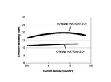
- 4 is data showing current density and light emission efficiency in a light emitting device in which the charge generation layer has the structure shown in FIG.
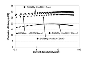
- FIG. 5 is data showing current density and light emission efficiency in a light emitting device in which the charge generation layer has the structure shown in FIG. 4.
- FIG. 1 is a cross-sectional view illustrating a configuration of a light emitting device 10 according to the embodiment.
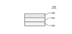
- 2 is a cross-sectional view showing the configuration of the organic layer 120 shown in FIG. 1
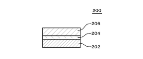
- FIG. 3 is a cross-sectional view showing the configuration of the charge generation layer 200 shown in FIG.
- the light emitting device 10 includes a first electrode 110, a second electrode 130, a plurality of organic layers 120, and a charge generation layer 200.
- the plurality of organic layers 120 are located between the first electrode 110 and the second electrode 130, and each has a light emitting layer 124 as shown in FIG. 2.
- the charge generation layer 200 is located between the adjacent organic layers 120.
- the charge generation layer 200 includes a first layer 202 and a second layer 204.
- the first layer 202 includes an electron transport material
- the second layer 204 includes a metal and a hole injection material.
- the charge generation layer 200 includes an electron injection material that improves the electron injection property of the first layer 202 closer to the first layer 202 than the second layer 204.
- the electron injection material is included in the first layer 202. Details will be described below.
- the light emitting device 10 is formed using a substrate 100.
- the substrate 100 is formed of a light transmissive material such as glass or a light transmissive resin.
- the substrate 100 may be formed of a material that does not have translucency.
- the substrate 100 is, for example, a polygon such as a rectangle.
- the substrate 100 may have flexibility.
- the thickness of the substrate 100 is, for example, not less than 10 ⁇ m and not more than 1000 ⁇ m.
- the thickness of the substrate 100 is, for example, 200 ⁇ m or less.
- the substrate 100 is a resin
- the substrate 100 is formed using, for example, PEN (polyethylene naphthalate), PES (polyethersulfone), PET (polyethylene terephthalate), or polyimide.
- an inorganic barrier film such as SiN x or SiON is formed on at least the light emitting surface side (preferably both surfaces) of the substrate 100 in order to suppress moisture from passing through the substrate 100. ing.
- a light emitting unit 140 is formed on the substrate 100.
- the light emitting unit 140 has an organic EL element.
- the organic EL element has a configuration in which a first electrode 110, a plurality of organic layers 120, and a second electrode 130 are laminated in this order.
- a charge generation layer 200 is provided between the plurality of organic layers 120.
- the light emitting device 10 has two organic layers 120.
- the charge generation layer 200 connects these two organic layers 120. If the organic layer 120 has a multi-photon structure, three (so-called tridem structure) or more may be formed. In this case, the charge generation layer 200 is provided at two locations between the organic layers 120.
- the first electrode 110 is a transparent electrode having optical transparency.
- the transparent conductive material constituting the transparent electrode is a metal-containing material, for example, a metal oxide such as ITO (Indium Tin Oxide), IZO (Indium Zinc Oxide), IWZO (Indium Tungsten Zinc Oxide), ZnO (Zinc Oxide), and the like. is there.
- the thickness of the first electrode 110 is, for example, not less than 10 nm and not more than 500 nm.
- the first electrode 110 is formed using, for example, a sputtering method or a vapor deposition method.
- the first electrode 110 may be a carbon nanotube or a conductive organic material such as PEDOT / PSS.
- the second electrode 130 is made of, for example, a metal selected from the first group consisting of Al, Au, Ag, Pt, Mg, Sn, Zn, and In or an alloy of a metal selected from the first group. Contains a metal layer. In this case, the second electrode 130 has a light shielding property.
- the thickness of the second electrode 130 is, for example, not less than 10 nm and not more than 500 nm. However, the second electrode 130 may be formed using the material exemplified as the material of the first electrode 110.
- the second electrode 130 is formed using, for example, a sputtering method or a vapor deposition method.
- the materials of the first electrode 110 and the second electrode 130 described above are examples in which light is transmitted through the substrate 100, that is, light emission from the light emitting device 10 is performed through the substrate 100 (bottom emission type). It is. In other cases, light may pass through the side opposite to the substrate 100. That is, the light emission from the light emitting device 10 is performed without passing through the substrate 100 (top emission type).
- the top emission type includes two types of laminated structures: a reverse product type and a forward product type. In the reverse product type, the material of the first electrode 110 and the material of the second electrode 130 are opposite to those of the bottom emission type. That is, the material of the second electrode 130 is used as the material of the first electrode 110, and the material of the first electrode 110 is used as the material of the second electrode 130.
- the material of the first electrode 110 is formed on the material of the second electrode 130 described above, the organic layer is further formed thereon, and the second electrode 130 is formed on the organic layer.
- the light is extracted from the side opposite to the substrate 100.
- the light emitting device 10 according to the present embodiment may be of any structure of a bottom emission type and the above two types of top emission types.
- the organic layer 120 has a light emitting layer 124.
- the organic layer 120 has a configuration in which a hole injection layer 122, a light emitting layer 124, and an electron injection layer 126 are stacked.
- a hole transport layer may be formed between the hole injection layer 122 and the light emitting layer 124.
- An electron transport layer may be formed between the light emitting layer 124 and the electron injection layer 126.
- the organic layer 120 may be formed by a vacuum deposition method.
- at least one layer of the organic layer 120 for example, a layer in contact with the first electrode 110 (the hole injection layer 122 in the example shown in FIG. 2) is applied by an application method such as an inkjet method, a printing method, or a spray method. May be formed.
- the remaining layers of the organic layer 120 may be formed by a vacuum evaporation method or may be formed by a coating method.
- the first electrode 110 side is formed by a coating method
- the second electrode 130 side through the charge generation layer 200 is formed by a vacuum evaporation method. 120 may be formed by different methods.
- the charge generation layer 200 has a first layer 202 and a second layer 204.
- the first layer 202 and the second layer 204 are formed using, for example, a vacuum evaporation method.
- the first layer 202 includes an electron transport material.
- This electron transporting material is, for example, Bphen (4,7-Diphenyl-1,10-phenanthroline).
- other electron transporting materials may be used for the first layer 202.
- Examples of other organic compounds having an electron transporting property include metal complexes having at least one 8-quinolinolato or a derivative thereof such as Alq 3 [tris (8-quinolinolato) aluminum] as a ligand, TAZ [3- ( Triazole compounds such as 4-biphenyl) -5- (4-t-butylphenyl) -4-phenyl-1,2,4-triazole], PBD [2- (4-biphenyl) -5- (4-t Oxadiazole compounds such as (butyl) -1,3,4-oxadiazole] can be used.
- the first layer 202 includes an electron injection material that enhances the electron injection property of the electron transport material in addition to the electron transport material described above.
- this electron injection material for example, Liq (8-Hydroxyquinolinolato-lithium) can be used.
- the electron injection material is not limited to this.
- Electron injection materials further include oxides and fluorides of alkaline metals and alkaline earth metals such as LiF, Li 2 O, and Li 2 CO 3 , carbonates, alkali metals such as lithium, sodium, calcium, and cesium, Alkaline earth metals can be used.
- the thickness of the first layer 202 is, for example, not less than 5 nm and not more than 150 nm, preferably not less than 10 nm and not more than 50 nm.
- the second layer 204 contains a metal and a hole injection material.
- a hole injection material for example, a compound containing a hexaazatriphenylene derivative such as HATCN (1,4,5,8,9,12-hexaazatriphenylenehexacarbonitrile) can be used.
- HATCN hexaazatriphenylene derivative
- the chemical formula of HATCN is represented by the following chemical formula (1).
- the metal contained in the second layer 204 is preferably a second group metal, for example, Mg or Ca.
- the metal and the hole injection material may be heated and deposited on the substrate 100 in the same vacuum deposition apparatus.
- a heat source for depositing the hole injection material a resistance heating type heat source can be used.
- Mg is used as the metal contained in the second layer 204
- a resistance heating type heating source can be used as a heating source when the metal is deposited.
- the metal contained in the second layer 204 is Mg, when the organic layer 120 is formed by a resistance heating type vacuum vapor deposition method, it is not necessary to invest new equipment, and the manufacturing cost of the light emitting device 10 is reduced. Can be lowered.
- FIG. 10 shows data indicating current density and light emission efficiency in the light emitting device 10.
- the lower data in the graph is data of a light emitting element in which the second layer 204 is formed on the first layer 202 without containing metal, in other words, the second layer 204 is formed only of the hole injection material. (HATCN layer).
- the upper data in the graph is the same as the lower data in the graph for the first layer 202, and the second layer 204 contains a metal material (specifically, Mg) in a volume ratio of 10%.
- Mg metal material
- the light-emitting element to which the metal material is added has higher light emission efficiency than the light-emitting element in which the metal material is not added to the second layer 204. That is, it can be seen that when a metal material is added to the second layer 204, the merit (increase in luminance) of the tandem structure is increased.
- the thickness of the second layer 204 is, for example, not less than 20 nm and not more than 50 nm, but may be thinner than this.
- the thickness of the second layer 204 may be 1 nm or more and 10 nm or less.
- the volume content of the metal (for example, Mg) contained in the second layer 204 is preferably 10% or more, and more preferably 50% or more.
- the volume content is, for example, 90% or less.
- SIMS secondary ion mass spectrometry
- XRF X-ray fluorescence analysis
- the first electrode 110 is formed on the substrate 100.
- the organic layer 120, the charge generation layer 200, and the organic layer 120 are formed in this order. Note that the charge generation layer 200 and the organic layer 120 may be further formed at least once on the upper organic layer 120.
- the second electrode 130 is formed on the uppermost organic layer 120.
- the charge generation layer 200 includes the first layer 202 and the second layer 204.
- the first layer 202 includes an electron transport material
- the second layer 204 includes a metal and a hole injection material.
- FIG. 4 is a cross-sectional view illustrating a configuration of the charge generation layer 200 included in the light emitting device 10 according to the second embodiment.
- FIG. 4 corresponds to FIG. 3 of the first embodiment.
- the light emitting device 10 according to the present embodiment has the same configuration as that of the light emitting device 10 according to the first embodiment except for the configuration of the charge generation layer 200.
- the charge generation layer 200 has a configuration in which a first layer 202, a second layer 204, and a third layer 206 are stacked.
- the configuration of the first layer 202 and the configuration of the second layer 204 are the same as those in the first embodiment.
- the thickness of the second layer 204 may be thinner than that of the first embodiment, and is, for example, 1 nm to 30 nm, and more preferably 1 nm to 10 nm.
- the third layer 206 is formed using a hole injection material.
- This hole injection material is, for example, the same as the hole injection material included in the second layer 204, but may be another material.
- the third layer 206 is formed using, for example, a vacuum evaporation method.
- the thickness of the third layer 206 is, for example, not less than 1 nm and not more than 100 nm.
- the third layer 206 does not contain the metal contained in the second layer 204. However, the above-described metal may diffuse from the second layer 204 to the third layer 206. Even in this case, the metal content of the third layer 206 is lower than the metal content of the second layer 204.
- the metal concentration in the third layer 206 decreases as the distance from the second layer 204 increases.
- the second layer 204 and the third layer 206 are continuously formed using the same vapor deposition apparatus. Can be formed. Specifically, the second layer 204 is formed by depositing a metal while depositing a hole injection material. Then, when the thickness of the formed film reaches a necessary thickness as the second layer 204, the vapor deposition of the metal is finished while continuing the vapor deposition of the hole injection material. When such a method is used, it may be difficult to confirm the interface between the second layer 204 and the third layer 206.
- the charge generation layer 200 since the charge generation layer 200 includes the second layer 204, the charge generation efficiency in the charge generation layer 200 is increased as in the first embodiment. Therefore, the luminance of the light emitting unit 140 can be increased.
- the third layer 206 is formed on the second layer 204, the second layer 204 (that is, a layer containing a metal) can be made thinner than in the first embodiment. By reducing the thickness of the second layer 204, the light transmittance of the charge generation layer 200 can be increased. Therefore, not only the light emission from the organic layer 120 on the second electrode 130 side of the opaque electrode on the bottom emission side described above, but also the light emission from the organic layer 120 on the first electrode 110 side reflects the opaque electrode. Since the light is extracted outside, the light extraction efficiency of the light emitting device 10 is improved.
- FIG. 11 is a graph showing the relationship between the light emission efficiency and the current density of the light emitting device 10 according to this embodiment.
- the thickness of the second layer 204 was changed between 2 nm and 20 nm, and the volume ratio of Mg was changed between 10%, 50%, and 80%. From this graph, it can be seen that the luminous efficiency of the light emitting device 10 increases when the thickness of the second layer 204 is changed from 5 nm to 2 nm.
- FIG. 5 is a cross-sectional view illustrating a configuration of the charge generation layer 200 included in the light emitting device 10 according to the modification.
- FIG. 5 corresponds to FIG. 4 of the second embodiment.
- the light emitting device 10 according to this embodiment has the same configuration as that of the light emitting device 10 according to the first embodiment or the second embodiment, except for the configuration of the charge generation layer 200. This figure shows a case similar to that of the second embodiment.
- the first layer 202 does not contain an electron injection material.
- the charge generation layer 200 includes an electron injection layer 208 below the second layer 204 (for example, between the first layer 202 and the second layer 204).
- the electron injection layer 208 is formed using, for example, Liq.
- the electron injection layer 208 is formed using another electron injection material such as an alkali metal or alkaline earth metal oxide or fluoride such as Li 2 O, LiF, or Li 2 CO 3 , or a carbonate alkali metal compound. May be.
- the charge generation layer 200 includes the second layer 204, so that the charge generation efficiency in the charge generation layer 200 is increased as in the first embodiment. Therefore, the luminance of the light emitting unit 140 can be increased.
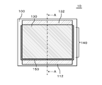
- FIG. 6 is a plan view illustrating the configuration of the light emitting device 10 according to the first embodiment.
- FIG. 7 is a view in which the second electrode 130 is removed from FIG. 6.
- FIG. 8 is a diagram in which the organic layer 120, the charge generation layer 200, and the insulating layer 150 are removed from FIG.
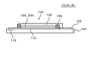
- FIG. 9 is a cross-sectional view taken along the line AA in FIG.
- the light emitting device 10 is a lighting device, and includes a substrate 100 and a light emitting unit 140.
- substrate 100 and the light emission part 140 is as the embodiment. Therefore, a plurality of organic layers 120 and a charge generation layer 200 are formed between the first electrode 110 and the second electrode 130.
- the edge of the first electrode 110 is covered with an insulating layer 150.
- the insulating layer 150 is made of, for example, a photosensitive resin material such as polyimide, and surrounds a portion of the first electrode 110 that becomes a light emitting region of the light emitting unit 140. By providing the insulating layer 150, it is possible to suppress a short circuit between the first electrode 110 and the second electrode 130 at the edge of the first electrode 110.
- the insulating layer 150 is formed, for example, by applying a resin material to be the insulating layer 150 and then exposing and developing the resin material.
- the light emitting device 10 has a first terminal 112 and a second terminal 132.
- the first terminal 112 is connected to the first electrode 110
- the second terminal 132 is connected to the second electrode 130.
- the first terminal 112 and the second terminal 132 include a layer formed of the same material as that of the first electrode 110.
- a lead wiring may be provided between the first terminal 112 and the first electrode 110.
- a lead wiring may be provided between the second terminal 132 and the second electrode 130.
- the first electrode 110 is formed on the substrate 100.
- the first terminal 112 and the second terminal 132 are also formed.
- the insulating layer 150, the organic layer 120, the charge generation layer 200, and the second electrode 130 are formed in this order.
- the charge generation layer 200 since the charge generation layer 200 includes the second layer 204, the charge generation efficiency in the charge generation layer 200 is increased as in the first embodiment. Therefore, the luminance of the light emitting unit 140 can be increased.
Landscapes
- Physics & Mathematics (AREA)
- Optics & Photonics (AREA)
- Engineering & Computer Science (AREA)
- Manufacturing & Machinery (AREA)
- Electroluminescent Light Sources (AREA)
Abstract
Description
第2電極と、
前記第1電極と前記第2電極の間に位置し、それぞれが発光層を含む複数の有機層と、
隣り合う2つの前記有機層の間に位置する電荷発生層と、
を備え、
前記電荷発生層は、
電子輸送性材料を含む第1層と、
金属及び正孔注入材料を含む第2層と、
正孔注入材料を含む第3層と、
を有し、
前記電荷発生層は、前記第2層及び前記第1層の間または前記第1層に、電子注入材料を含み、
前記第3層において前記金属の含有率は、前記第2層における前記金属の含有率よりも低い発光装置である。
図1は、実施形態に係る発光装置10の構成を示す断面図である。図2は、図1に示した有機層120の構成を示す断面図であり、図3は、図1に示した電荷発生層200の構成を示す断面図である。図1に示すように、発光装置10は、第1電極110、第2電極130、複数の有機層120、及び電荷発生層200を備えている。複数の有機層120は第1電極110と第2電極130の間に位置しており、図2に示すように、それぞれが発光層124を有している。電荷発生層200は隣り合う有機層120の間に位置している。言い換えると、複数の有機層120は互いに積層されているが、これら複数の有機層120の間には電荷発生層200が設けられている。また、有機層120のことを発光ユニットと表現することもできる。発光装置10は電荷発生層200を介して発光色の異なる複数の発光ユニットを有することもできる。電荷発生層200は、図3に示すように、第1層202及び第2層204を有している。第1層202は電子輸送性材料を含んでおり、第2層204は金属及び正孔注入材料を含んでいる。また、電荷発生層200は、第2層204より第1層202側に、第1層202の電子注入性を高める電子注入材料を含んでいる。図3に示す例では、電子注入材料は第1層202に含まれている。以下、詳細に説明する。

図4は、第2の実施形態に係る発光装置10が有する電荷発生層200の構成を示す断面図である。図4は、第1の実施形態の図3に対応している。本実施形態に係る発光装置10は、電荷発生層200の構成を除いて第1の実施形態に係る発光装置10と同様の構成である。
図5は、変形例に係る発光装置10が有する電荷発生層200の構成を示す断面図である。図5は、第2の実施形態の図4に対応している。本実施形態に係る発光装置10は、電荷発生層200の構成を除いて、第1の実施形態又は第2の実施形態に係る発光装置10と同様の構成である。本図は、第2の実施形態と同様の場合を示している。
図6は、実施例1に係る発光装置10の構成を示す平面図である。図7は、図6から第2電極130を取り除いた図である。図8は図7から有機層120、電荷発生層200、及び絶縁層150を取り除いた図である。図9は図6のA-A断面図である。
Claims (7)
- 第1電極と、
第2電極と、
前記第1電極と前記第2電極の間に位置し、それぞれが発光層を含む複数の有機層と、
隣り合う2つの前記有機層の間に位置する電荷発生層と、
を備え、
前記電荷発生層は、
電子輸送性材料を含む第1層と、
金属及び正孔注入材料を含む第2層と、
正孔注入材料を含む第3層と、
を有し、
前記電荷発生層は、前記第2層及び前記第1層の間または前記第1層に、電子注入材料を含み、
前記第3層において前記金属の含有率は、前記第2層における前記金属の含有率よりも低い発光装置。 - 請求項1に記載の発光装置において、
前記金属は第2属の金属である発光装置。 - 請求項2に記載の発光装置において、
前記金属はMgである発光装置。 - 請求項3に記載の発光装置において、
前記第2層におけるMgの体積含有率は10%以上である発光装置。 - 請求項1~4のいずれか一項に記載の発光装置において、
前記第2層の厚さは1nm以上10nm以下である発光装置。 - 請求項1~5のいずれか一項に記載の発光装置において、
前記電子注入材料は前記第1層に含まれる発光装置。 - 請求項1~6のいずれか一項に記載の発光装置において、
前記第2層と前記有機層の間に、前記電子注入材料を含む電子注入層を有する発光装置。
Priority Applications (3)
| Application Number | Priority Date | Filing Date | Title |
|---|---|---|---|
| JP2017505896A JP6419940B2 (ja) | 2015-03-16 | 2015-03-16 | 発光装置 |
| PCT/JP2015/057633 WO2016147285A1 (ja) | 2015-03-16 | 2015-03-16 | 発光装置 |
| US15/558,173 US9991461B2 (en) | 2015-03-16 | 2015-03-16 | Light emitting device |
Applications Claiming Priority (1)
| Application Number | Priority Date | Filing Date | Title |
|---|---|---|---|
| PCT/JP2015/057633 WO2016147285A1 (ja) | 2015-03-16 | 2015-03-16 | 発光装置 |
Publications (1)
| Publication Number | Publication Date |
|---|---|
| WO2016147285A1 true WO2016147285A1 (ja) | 2016-09-22 |
Family
ID=56918800
Family Applications (1)
| Application Number | Title | Priority Date | Filing Date |
|---|---|---|---|
| PCT/JP2015/057633 Ceased WO2016147285A1 (ja) | 2015-03-16 | 2015-03-16 | 発光装置 |
Country Status (3)
| Country | Link |
|---|---|
| US (1) | US9991461B2 (ja) |
| JP (1) | JP6419940B2 (ja) |
| WO (1) | WO2016147285A1 (ja) |
Families Citing this family (1)
| Publication number | Priority date | Publication date | Assignee | Title |
|---|---|---|---|---|
| KR20220092736A (ko) * | 2020-12-24 | 2022-07-04 | 삼성디스플레이 주식회사 | 유기발광다이오드 및 이를 포함하는 디스플레이 장치 |
Citations (4)
| Publication number | Priority date | Publication date | Assignee | Title |
|---|---|---|---|---|
| WO2011010696A1 (ja) * | 2009-07-23 | 2011-01-27 | 株式会社カネカ | 有機エレクトロルミネッセント素子 |
| JP2012195054A (ja) * | 2011-03-14 | 2012-10-11 | Idemitsu Kosan Co Ltd | 有機エレクトロルミネッセンス素子 |
| JP2014110421A (ja) * | 2013-10-18 | 2014-06-12 | Panasonic Corp | 有機エレクトロルミネッセンス素子 |
| JP2014225470A (ja) * | 2009-05-29 | 2014-12-04 | 株式会社半導体エネルギー研究所 | 発光素子、発光装置、電子機器及び照明装置 |
Family Cites Families (10)
| Publication number | Priority date | Publication date | Assignee | Title |
|---|---|---|---|---|
| US6869699B2 (en) * | 2003-03-18 | 2005-03-22 | Eastman Kodak Company | P-type materials and mixtures for electronic devices |
| US7273663B2 (en) | 2004-08-20 | 2007-09-25 | Eastman Kodak Company | White OLED having multiple white electroluminescence units |
| KR101316752B1 (ko) * | 2007-05-31 | 2013-10-08 | 삼성디스플레이 주식회사 | 백색 유기발광소자 |
| JP2010192719A (ja) | 2009-02-19 | 2010-09-02 | Yamagata Promotional Organization For Industrial Technology | 有機エレクトロルミネッセンス素子 |
| US8987726B2 (en) | 2009-07-23 | 2015-03-24 | Kaneka Corporation | Organic electroluminescent element |
| JP2013545249A (ja) * | 2010-12-09 | 2013-12-19 | ▲海▼洋王照明科技股▲ふん▼有限公司 | 両面発光有機エレクトロルミネッセンスデバイス及びその製造方法 |
| JP2012199231A (ja) * | 2011-03-04 | 2012-10-18 | Semiconductor Energy Lab Co Ltd | 表示装置 |
| DE102012211869A1 (de) * | 2012-07-06 | 2014-01-09 | Osram Opto Semiconductors Gmbh | Organisches Licht emittierendes Bauelement |
| KR102135929B1 (ko) * | 2013-12-31 | 2020-07-20 | 엘지디스플레이 주식회사 | 백색 유기 발광 소자 |
| CN104218165A (zh) * | 2014-08-20 | 2014-12-17 | 京东方科技集团股份有限公司 | 一种有机发光二极管器件及显示装置 |
-
2015
- 2015-03-16 WO PCT/JP2015/057633 patent/WO2016147285A1/ja not_active Ceased
- 2015-03-16 JP JP2017505896A patent/JP6419940B2/ja active Active
- 2015-03-16 US US15/558,173 patent/US9991461B2/en active Active
Patent Citations (4)
| Publication number | Priority date | Publication date | Assignee | Title |
|---|---|---|---|---|
| JP2014225470A (ja) * | 2009-05-29 | 2014-12-04 | 株式会社半導体エネルギー研究所 | 発光素子、発光装置、電子機器及び照明装置 |
| WO2011010696A1 (ja) * | 2009-07-23 | 2011-01-27 | 株式会社カネカ | 有機エレクトロルミネッセント素子 |
| JP2012195054A (ja) * | 2011-03-14 | 2012-10-11 | Idemitsu Kosan Co Ltd | 有機エレクトロルミネッセンス素子 |
| JP2014110421A (ja) * | 2013-10-18 | 2014-06-12 | Panasonic Corp | 有機エレクトロルミネッセンス素子 |
Also Published As
| Publication number | Publication date |
|---|---|
| US9991461B2 (en) | 2018-06-05 |
| JP6419940B2 (ja) | 2018-11-07 |
| US20180076409A1 (en) | 2018-03-15 |
| JPWO2016147285A1 (ja) | 2017-12-14 |
Similar Documents
| Publication | Publication Date | Title |
|---|---|---|
| CN100361311C (zh) | 显示装置和采用该显示装置的单元 | |
| JP4898560B2 (ja) | 有機発光装置 | |
| JP5411469B2 (ja) | 発光装置および電子機器、発光装置の製造方法 | |
| JP5584319B2 (ja) | 有機電界発光素子、照明装置及び照明システム | |
| EP3038178B1 (en) | Organic electroluminescent device and organic electroluminescent display device | |
| US9647232B2 (en) | Organic electroluminescent device, illumination apparatus, and illumination system | |
| US8710735B2 (en) | Organic electroluminescence element | |
| US20100051991A1 (en) | Organic el device and process of producing the same | |
| JP4254668B2 (ja) | 有機電界発光素子および表示装置 | |
| US20160372697A1 (en) | Organic electroluminescent element and method for manufacturing same | |
| JP4872805B2 (ja) | 有機エレクトロルミネッセンス素子 | |
| JP5297400B2 (ja) | 発光装置 | |
| JP6419940B2 (ja) | 発光装置 | |
| JP7635042B2 (ja) | 有機エレクトロルミネッセント素子、ディスプレイ装置、照明装置 | |
| JP2023041929A (ja) | 発光装置 | |
| JP2016171047A (ja) | 発光装置 | |
| JP2010033973A (ja) | 有機エレクトロルミネッセンス素子 | |
| TWI321966B (en) | Organic electro-luminescence device and method of manufacturing the same | |
| CN109509843B (zh) | 发光元件及其透明电极 | |
| JP2017091775A (ja) | 発光装置の製造方法 | |
| WO2014084159A1 (ja) | 有機el素子及びその製造方法 | |
| JP2020102654A (ja) | 発光装置 | |
| JP2006127969A (ja) | 有機el素子 | |
| JP2014093130A (ja) | 電子デバイス及びその製造方法 | |
| JP6688814B2 (ja) | 発光装置 |
Legal Events
| Date | Code | Title | Description |
|---|---|---|---|
| 121 | Ep: the epo has been informed by wipo that ep was designated in this application |
Ref document number: 15885383 Country of ref document: EP Kind code of ref document: A1 |
|
| ENP | Entry into the national phase |
Ref document number: 2017505896 Country of ref document: JP Kind code of ref document: A |
|
| WWE | Wipo information: entry into national phase |
Ref document number: 15558173 Country of ref document: US |
|
| NENP | Non-entry into the national phase |
Ref country code: DE |
|
| 122 | Ep: pct application non-entry in european phase |
Ref document number: 15885383 Country of ref document: EP Kind code of ref document: A1 |