WO2016136774A1 - フィルム状接着剤、接着シートおよび半導体装置の製造方法 - Google Patents
フィルム状接着剤、接着シートおよび半導体装置の製造方法 Download PDFInfo
- Publication number
- WO2016136774A1 WO2016136774A1 PCT/JP2016/055344 JP2016055344W WO2016136774A1 WO 2016136774 A1 WO2016136774 A1 WO 2016136774A1 JP 2016055344 W JP2016055344 W JP 2016055344W WO 2016136774 A1 WO2016136774 A1 WO 2016136774A1
- Authority
- WO
- WIPO (PCT)
- Prior art keywords
- adhesive
- film
- chip
- mass
- film adhesive
- Prior art date
- Legal status (The legal status is an assumption and is not a legal conclusion. Google has not performed a legal analysis and makes no representation as to the accuracy of the status listed.)
- Ceased
Links
Classifications
-
- C—CHEMISTRY; METALLURGY
- C09—DYES; PAINTS; POLISHES; NATURAL RESINS; ADHESIVES; COMPOSITIONS NOT OTHERWISE PROVIDED FOR; APPLICATIONS OF MATERIALS NOT OTHERWISE PROVIDED FOR
- C09J—ADHESIVES; NON-MECHANICAL ASPECTS OF ADHESIVE PROCESSES IN GENERAL; ADHESIVE PROCESSES NOT PROVIDED FOR ELSEWHERE; USE OF MATERIALS AS ADHESIVES
- C09J7/00—Adhesives in the form of films or foils
- C09J7/10—Adhesives in the form of films or foils without carriers
-
- C—CHEMISTRY; METALLURGY
- C09—DYES; PAINTS; POLISHES; NATURAL RESINS; ADHESIVES; COMPOSITIONS NOT OTHERWISE PROVIDED FOR; APPLICATIONS OF MATERIALS NOT OTHERWISE PROVIDED FOR
- C09J—ADHESIVES; NON-MECHANICAL ASPECTS OF ADHESIVE PROCESSES IN GENERAL; ADHESIVE PROCESSES NOT PROVIDED FOR ELSEWHERE; USE OF MATERIALS AS ADHESIVES
- C09J201/00—Adhesives based on unspecified macromolecular compounds
-
- H—ELECTRICITY
- H10—SEMICONDUCTOR DEVICES; ELECTRIC SOLID-STATE DEVICES NOT OTHERWISE PROVIDED FOR
- H10W—GENERIC PACKAGES, INTERCONNECTIONS, CONNECTORS OR OTHER CONSTRUCTIONAL DETAILS OF DEVICES COVERED BY CLASS H10
- H10W72/00—Interconnections or connectors in packages
- H10W72/071—Connecting or disconnecting
-
- C—CHEMISTRY; METALLURGY
- C09—DYES; PAINTS; POLISHES; NATURAL RESINS; ADHESIVES; COMPOSITIONS NOT OTHERWISE PROVIDED FOR; APPLICATIONS OF MATERIALS NOT OTHERWISE PROVIDED FOR
- C09J—ADHESIVES; NON-MECHANICAL ASPECTS OF ADHESIVE PROCESSES IN GENERAL; ADHESIVE PROCESSES NOT PROVIDED FOR ELSEWHERE; USE OF MATERIALS AS ADHESIVES
- C09J2203/00—Applications of adhesives in processes or use of adhesives in the form of films or foils
- C09J2203/326—Applications of adhesives in processes or use of adhesives in the form of films or foils for bonding electronic components such as wafers, chips or semiconductors
Definitions
- the present invention relates to a film-like adhesive and an adhesive sheet particularly suitable for use in a step of die-bonding a semiconductor element (semiconductor chip) to an organic substrate, a lead frame, another semiconductor chip, or the like.
- the present invention also relates to a method for manufacturing a semiconductor device using the film adhesive and the adhesive sheet.
- silicon wafers are processed as thin as possible and multi-layered to increase the capacity.
- an ultra-thin wafer processing method has become a key point, and various thin processing methods have been devised and evaluated.
- a method of manufacturing a semiconductor chip by forming a groove having a predetermined depth from the front side of the wafer and then grinding from the back side is disclosed.
- Such a process is also called “first dicing method”.
- the prior dicing method it is possible to manufacture a chip while minimizing the damage of the thinned wafer.
- the chip manufactured in this way is transferred onto a die attach film (DAF) from a back grind tape that is usually attached to the circuit surface side of the wafer during grinding.
- DAF die attach film
- the DAF is attached to the wafer, it is diced together with the wafer and separated into individual pieces.
- the wafer separated into chips is transferred onto the DAF, it is necessary to divide only the DAF into the same size as the chip.
- laser dicing with laser light is suitable as a DAF dividing method.
- the laser dicing apparatus is expensive, and as a result, the manufacturing cost of the semiconductor device increases.
- Patent Document 1 Japanese Patent Laid-Open No. 2012-164953 describes a method for dividing DAF by high-pressure air.
- the DAF dividing method described in Patent Document 1 is difficult to divide DAF depending on the conditions and the composition of DAF.
- the present invention has been made in view of the above situation, and an object thereof is to provide a film adhesive and an adhesive sheet suitable for a dividing method using a heated gas. Another object of the present invention is to provide a method for manufacturing a semiconductor device using the film adhesive and the adhesive sheet.
- the present invention for solving the above problems includes the following gist.
- a film adhesive comprising a polymer component (A) and a thermosetting component (B1),
- the content of the polymer component (A) in the film adhesive is 1 to 30% by mass
- the content of the thermosetting component (B1) is 40 to 70% by mass
- a film adhesive used for fusing the film adhesive by sticking the film adhesive to a chip group composed of a plurality of chip bodies and releasing a heated gas toward the film adhesive.
- the chip group composed of the plurality of chip bodies is an area on the surface of the work, and a groove is provided in an area other than the area remaining as the chip body after the work is separated into pieces.
- a method of manufacturing a semiconductor device including the following steps (a) and (b): (A) The polymer component (A) and the thermosetting component (B1) are included, the content of the polymer component (A) is 1 to 30% by mass, and the content of the thermosetting component (B1) is 40 to 70.
- step (c) A groove is provided in an area on the surface of the work other than the area remaining as a chip body after the work is separated into pieces, and the work thinning process is performed from the back side of the work to the bottom of the groove.
- the present invention it is easy to divide DAF with heated gas. Therefore, the initial investment cost and maintenance cost of the laser dicing apparatus can be suppressed, and the cost can be reduced as compared with the DAF dividing method by laser dicing.
- the functions required at least for the film adhesive according to the present invention are (1) sheet shape maintenance, (2) initial adhesion, and (3) curability.
- a binder component containing the polymer component (A) and the thermosetting component (B1) By adding a binder component containing the polymer component (A) and the thermosetting component (B1), (1) sheet shape maintaining property and (3) curability can be imparted to the film adhesive. In addition, it is a function for making it adhere temporarily to a to-be-adhered body (chip group which consists of a some chip body) until a film adhesive hardens
- Initial adhesiveness is pressure sensitive adhesiveness. It may be a property of being softened and bonded by heat. (2) The initial adhesiveness is usually controlled by adjusting various properties of the binder component and adjusting the blending amount of the inorganic filler (D) described later.
- the polymer component (A) is added to the film adhesive mainly for the purpose of imparting sheet shape maintainability to the film adhesive.
- the weight average molecular weight (Mw) of the polymer component (A) is usually 20,000 or more, preferably 20,000 to 3,000,000.
- the value of the weight average molecular weight (Mw) is a value when measured by a gel permeation chromatography (GPC) method (polystyrene standard).
- the measurement by such a method is carried out by, for example, using a high-speed column “TSK gel column H XL- H”, “TSK Gel GMH XL ”, “TSK Gel G2000H XL ”
- the detector is used as a differential refractometer under the conditions of column temperature: 40 ° C. and liquid feed rate: 1.0 mL / min.
- acrylic polymers acrylic polymers, polyesters, phenoxy resins, polycarbonates, polyethers, polyurethanes, polysiloxanes, rubber polymers, and the like can be used. Further, it is an acrylic urethane resin obtained by reacting a urethane prepolymer having an isocyanate group at a molecular terminal with an acrylic polyol which is an acrylic polymer having a hydroxyl group, which is a combination of two or more of these. May be. Furthermore, two or more of these may be used in combination, including a polymer in which two or more are bonded.
- the content of the polymer component (A) in the film adhesive is 1 to 30% by mass, preferably 4 to 15% by mass.
- acrylic polymer (A1) As the acrylic polymer polymer component (A), acrylic polymer (A1) is preferably used.
- the acrylic polymer (A1) is a polymer containing a structural unit formed by polymerizing a (meth) acrylic acid ester described later.
- the proportion of the structural unit formed by polymerizing the (meth) acrylic acid ester in the acrylic polymer (A1) is usually 40% by mass or more, preferably 50% by mass or more, more preferably 60% by mass or more, and particularly preferably. Is 70% by mass or more.
- the ratio of the structural unit contained in the acrylic polymer (A1) is usually the ratio of monomers that can form each structural unit in all monomers used for the polymerization of the acrylic polymer (A1) ( It matches the charging ratio).
- the glass transition temperature (Tg) of the acrylic polymer (A1) is preferably in the range of ⁇ 60 to 50 ° C., more preferably ⁇ 50 to 40 ° C., and further preferably ⁇ 40 to 30 ° C.
- Tg glass transition temperature
- the glass transition temperature of the acrylic polymer (A1) is too low, as described later, when the film adhesive is formed on the support, the peeling force between the film adhesive and the support becomes large. Transfer failure of the film adhesive may occur, and if it is too high, the adhesive property of the film adhesive will decrease, and transfer to the adherend will not be possible, or the film adhesive will peel off from the adherend after transfer, etc. May occur.
- the weight average molecular weight of the acrylic polymer (A1) is more preferably 100,000 to 1,500,000. If the weight average molecular weight of the acrylic polymer (A1) is too low, the adhesion between the film adhesive and the support becomes high, and transfer failure of the film adhesive may occur. Adhesiveness of the adhesive may be reduced, and transfer to the adherend may not be possible, or defects such as peeling of the film adhesive from the adherend after transfer may occur.
- the acrylic polymer (A1) contains (meth) acrylic acid ester in at least a constituent monomer.
- (meth) acrylic acid esters include alkyl (meth) acrylates having an alkyl group having 1 to 18 carbon atoms, specifically methyl (meth) acrylate, ethyl (meth) acrylate, propyl (meth) acrylate, butyl ( (Meth) acrylate, 2-ethylhexyl (meth) acrylate, etc .; (meth) acrylate having a cyclic skeleton, specifically cycloalkyl (meth) acrylate, benzyl (meth) acrylate, isobornyl (meth) acrylate, dicyclopentanyl ( Examples include meth) acrylate, dicyclopentenyl (meth) acrylate, dicyclopentenyloxyethyl (meth) acrylate, and imide (meth) acrylate. Moreover, what is (meth
- (meth) acryl may be used to include both acrylic and methacryl.
- a monomer having a hydroxyl group may be used as the monomer constituting the acrylic polymer (A1).
- the monomer having a hydroxyl group include (meth) acrylic acid ester having a hydroxyl group such as 2-hydroxylethyl (meth) acrylate and 2-hydroxypropyl (meth) acrylate; N-methylol (meth) acrylamide and the like.
- a monomer having a carboxyl group may be used as the monomer constituting the acrylic polymer (A1).
- a monomer having a carboxyl group may be used.
- the monomer having a carboxyl group include (meth) acrylic acid, maleic acid, fumaric acid, and itaconic acid.
- an epoxy thermosetting component as the thermosetting component (B1) described later, the carboxyl group and the epoxy group in the epoxy thermosetting component react with each other. The amount used is preferably small.
- a monomer having an amino group may be used as a monomer constituting the acrylic polymer (A1).
- a monomer having an amino group examples include (meth) acrylic acid esters having an amino group such as monoethylamino (meth) acrylate.
- the monomer constituting the acrylic polymer (A1) vinyl acetate, styrene, ethylene, ⁇ -olefin and the like may be used.
- the acrylic polymer (A1) may be cross-linked.
- Crosslinking is performed by adding a crosslinking agent to the composition for forming a film adhesive, in which the acrylic polymer (A1) before crosslinking has a crosslinkable functional group such as a hydroxyl group. This is carried out by the reaction of the functional group with the functional group of the crosslinking agent.
- crosslinking agent examples include organic polyvalent isocyanate compounds and organic polyvalent imine compounds.
- organic polyvalent isocyanate compounds include aromatic polyvalent isocyanate compounds, aliphatic polyvalent isocyanate compounds, alicyclic polyvalent isocyanate compounds, trimers of these organic polyvalent isocyanate compounds, and these organic polyvalent isocyanate compounds.
- examples thereof include terminal isocyanate urethane prepolymers obtained by reacting with a polyol compound.
- organic polyvalent isocyanate compound examples include 2,4-tolylene diisocyanate, 2,6-tolylene diisocyanate, 1,3-xylylene diisocyanate, 1,4-xylene diisocyanate, diphenylmethane-4,4′-.
- organic polyvalent imine compounds include N, N′-diphenylmethane-4,4′-bis (1-aziridinecarboxamide), trimethylolpropane-tri- ⁇ -aziridinylpropionate, tetramethylol. Mention may be made of methane-tri- ⁇ -aziridinylpropionate and N, N′-toluene-2,4-bis (1-aziridinecarboxamide) triethylenemelamine.
- the crosslinking agent is usually 0.01 to 20 parts by weight, preferably 0.1 to 10 parts by weight, more preferably 0.5 to 5 parts by weight with respect to 100 parts by weight of the acrylic polymer (A1) before crosslinking. Used in ratio.
- the polymer component (A) when the content of the component constituting the film adhesive is determined on the basis of the content of the polymer component (A), the polymer component (A) is a crosslinked acrylic polymer.
- the reference content is the content of the acrylic polymer before being crosslinked.
- the polymer component (A) is selected from polyester, phenoxy resin, polycarbonate, polyether, polyurethane, polysiloxane, rubber polymer, or a combination of two or more thereof.
- One kind of acrylic resin (A2) or a combination of two or more kinds may be used.
- Such a resin preferably has a weight average molecular weight of 20,000 to 100,000, more preferably 20,000 to 80,000.
- the glass transition temperature of the non-acrylic resin (A2) is preferably in the range of ⁇ 30 to 150 ° C., more preferably in the range of ⁇ 20 to 120 ° C. If the glass transition temperature of the non-acrylic resin is too low, the peeling force between the film adhesive and the support may be increased, resulting in poor transfer of the film adhesive. There is a risk of insufficient adhesion to the body.
- non-acrylic resin (A2) is used in combination with the above-mentioned acrylic polymer (A1), delamination between the film-like adhesive and the support during transfer of the film-like adhesive to the adherend
- the film adhesive can follow the transfer surface and the generation of voids can be suppressed.
- the content of the non-acrylic resin (A2) is such that the non-acrylic resin (A2) and the acrylic polymer (
- the mass ratio (A2: A1) to A1) is usually in the range of 1:99 to 60:40, preferably 1:99 to 30:70.
- the content of the non-acrylic resin (A2) is in this range, the above effect can be obtained.
- curable polymer component Moreover, you may use a curable polymer component (AB) as a polymer component (A).
- the curable polymer component is a polymer having a curing functional group.
- the curing functional group is a functional group that can react with each other to form a three-dimensional network structure, and examples thereof include a functional group that reacts by heating and a functional group that reacts by energy rays.
- curable polymer component (AB) has sclerosis
- the functional functional group may be added to the unit of a continuous structure that becomes the skeleton of the curable polymer (AB) or may be added to the terminal.
- the functional functional group may be added to the side chain or directly to the main chain. You may do it.
- the weight average molecular weight (Mw) of the curable polymer component (AB) is usually 20,000 or more from the viewpoint of achieving the purpose of imparting sheet shape maintainability to the film adhesive.
- An example of a functional group that reacts by heating is an epoxy group.
- the curable polymer component (AB) having an epoxy group include a high molecular weight epoxy group-containing compound and a phenoxy resin having an epoxy group.
- High molecular weight epoxy group-containing compounds are disclosed, for example, in JP-A No. 2001-261789.
- it is a polymer similar to the above-mentioned acrylic polymer (A1), which is polymerized using a monomer having an epoxy group as a monomer (epoxy group-containing acrylic polymer). Also good.
- monomers include (meth) acrylic acid esters having a glycidyl group such as glycidyl (meth) acrylate.
- the preferred embodiment is the same as that of the acrylic polymer (A1).
- thermosetting component As in the case of using an epoxy group-containing curable polymer component (AB), as in the case of using an epoxy thermosetting component as the thermosetting component (B1), a thermosetting agent (B12) or a curing accelerator ( B13) may be used in combination.
- Examples of the functional group that reacts with energy rays include a (meth) acryloyl group.
- the curable polymer component (AB) having a functional group that reacts with energy rays an acrylate compound having a polymer structure such as polyether acrylate, and the like having a high molecular weight can be used.
- a polymer prepared by reacting a low molecular compound having a functional group that reacts with the above may be used.
- the preferred mode of the raw material polymer is the same as that of the acrylic polymer (A1).
- the photopolymerization initiator (B22) may be used in the same manner as when the energy ray curable component (B2) is used. .
- thermosetting component (B1) Thermosetting component
- the thermosetting component (B1) is added to the film adhesive mainly for the purpose of imparting curability to the film adhesive.
- the thermosetting component (B1) contains at least a compound having a functional group that reacts by heating. Curing is realized by the functional groups of the thermosetting component (B1) reacting to form a three-dimensional network structure. Since the thermosetting component (B1) is used in combination with the polymer component (A), from the viewpoint of suppressing the viscosity of the adhesive composition for forming the film adhesive and improving the handleability, etc.
- its weight average molecular weight (Mw) is 10,000 or less, preferably 100 to 10,000.
- the content of the thermosetting component (B1) in the film adhesive is 40 to 70% by mass, preferably 50 to 65% by mass, more preferably 50 to 60% by mass.
- thermosetting component (B1) for example, an epoxy-based thermosetting component is preferable.
- the epoxy thermosetting component preferably contains a compound (B11) having an epoxy group and a combination of a compound (B11) having an epoxy group and a thermosetting agent (B12).
- an epoxy-type thermosetting component may contain a hardening accelerator (B13).
- epoxy compound (B11) Compound having an epoxy group
- a conventionally known compound can be used. Specifically, polyfunctional epoxy resin, bisphenol A diglycidyl ether and its hydrogenated product, orthocresol novolac epoxy resin, dicyclopentadiene type epoxy resin, biphenyl type epoxy resin, bisphenol A type epoxy resin, bisphenol F type Examples thereof include epoxy compounds having two or more functional groups in the molecule, such as epoxy resins and phenylene skeleton type epoxy resins. These can be used individually by 1 type or in combination of 2 or more types.
- the film adhesive preferably contains 120 to 1500 parts by mass of the epoxy compound (B11), more preferably 100 parts by mass of the polymer component (A). Is included in an amount of 200 to 1200 parts by mass. If the epoxy compound (B11) is less than 120 parts by mass, sufficient adhesion may not be obtained, and if it exceeds 1500 parts by mass, the peel strength between the film adhesive and the support increases, and the film adhesive Transfer defects may occur.
- thermosetting agent (B12) functions as a curing agent for the epoxy compound (B11).
- a preferable thermosetting agent includes a compound having two or more functional groups capable of reacting with an epoxy group in one molecule. Examples of the functional group include a phenolic hydroxyl group, an alcoholic hydroxyl group, an amino group, a carboxyl group, and an acid anhydride. Of these, phenolic hydroxyl groups, amino groups, acid anhydrides and the like are preferable, and phenolic hydroxyl groups and amino groups are more preferable.
- phenolic curing agent examples include polyfunctional phenolic resins, biphenols, novolac type phenolic resins, dicyclopentadiene type phenolic resins, zylock type phenolic resins, and aralkylphenolic resins.
- amine curing agent is DICY (dicyandiamide). These can be used individually by 1 type or in mixture of 2 or more types.
- the content of the thermosetting agent (B12) is preferably 0.1 to 500 parts by mass and more preferably 1 to 200 parts by mass with respect to 100 parts by mass of the epoxy compound (B11). If the content of the thermosetting agent is small, the adhesiveness may not be obtained due to insufficient curing, and if it is excessive, the moisture absorption rate of the film adhesive may increase and the reliability of the semiconductor device may be reduced.
- the curing accelerator (B13) may be used to adjust the rate of thermal curing of the film adhesive.
- the curing accelerator (B13) is particularly preferably used when an epoxy thermosetting component is used as the thermosetting component (B1).
- Preferred curing accelerators include tertiary amines such as triethylenediamine, benzyldimethylamine, triethanolamine, dimethylaminoethanol, tris (dimethylaminomethyl) phenol; 2-methylimidazole, 2-phenylimidazole, 2-phenyl- Imidazoles such as 4-methylimidazole, 2-phenyl-4,5-dihydroxymethylimidazole and 2-phenyl-4-methyl-5-hydroxymethylimidazole; Organic phosphines such as tributylphosphine, diphenylphosphine and triphenylphosphine; And tetraphenylboron salts such as tetraphenylphosphonium tetraphenylborate and triphenylphosphinetetraphenylborate. These can be used individually by 1 type or in mixture of 2 or more types.
- the curing accelerator (B13) is preferably 0.01 to 10 parts by mass, more preferably 0.1 to 1 part by mass with respect to 100 parts by mass of the total amount of the epoxy compound (B11) and the thermosetting agent (B12). Included in the amount of.
- the curing accelerator (B13) By containing the curing accelerator (B13) in an amount within the above range, it has excellent adhesiveness even when exposed to high temperatures and high humidity, and has high reliability even when exposed to severe reflow conditions. Can be achieved.
- the content of the curing accelerator (B13) is small, sufficient adhesion cannot be obtained due to insufficient curing, and when it is excessive, the curing accelerator having high polarity is bonded to the film adhesive under high temperature and high humidity. The reliability of the semiconductor device is lowered by moving to the side and segregating.
- the film adhesive may contain an energy beam curable component (B2).
- the energy ray-curable component (B2) contains a compound (B21) having a functional group that reacts upon irradiation with energy rays, and is polymerized and cured when irradiated with energy rays such as ultraviolet rays and electron beams.
- the film adhesive contains both the thermosetting component (B1) and the energy ray curable component (B2), the film adhesive can be precured by energy ray irradiation before the thermosetting step.
- the adhesiveness at the interface between the die-bonding film adhesive and the support is controlled, and the process suitability of the film adhesive is improved in processes performed before the thermosetting process, such as the wire bonding process.
- a compound (B21) having a functional group that reacts by irradiation with energy rays may be used alone, but photopolymerization with a compound (B21) having a functional group that reacts by irradiation with energy rays. It is preferable to use a combination of initiators (B22).
- (B21) Compound having a functional group that reacts upon irradiation with energy rays
- Compound (B21) having a functional group that reacts upon irradiation with energy rays (hereinafter sometimes referred to as “energy ray-reactive compound (B21)”) Specifically, dicyclopentanyl dimethylene diacrylate, trimethylolpropane triacrylate, pentaerythritol triacrylate, pentaerythritol tetraacrylate, dipentaerythritol monohydroxypentaacrylate, dipentaerythritol hexaacrylate or 1,4-butylene glycol diacrylate Acrylate compounds such as 1,6-hexanediol diacrylate; oligoester acrylate, urethane acrylate oligomer, epoxy acrylate, poly A acrylate compound having a polymerizable structure acrylate compounds such as chromatography ether acrylate and itaconic acid
- the film adhesive preferably contains 1 to 1500 parts by mass of the energy ray reactive compound (B21) with respect to 100 parts by mass of the polymer component (A). More preferably, it is contained in an amount of 3 to 1200 parts by mass.
- photopolymerization initiator (B22) examples include benzophenone, acetophenone, benzoin, benzoin methyl ether, benzoin ethyl ether, benzoin isopropyl ether, benzoin isobutyl ether, benzoin benzoic acid, benzoin methyl benzoate, and benzoin dimethyl ketal.
- a photoinitiator (B22) can be used individually by 1 type or in combination of 2 or more types.
- the blending ratio of the photopolymerization initiator (B22) is preferably 0.1 to 10 parts by mass, and preferably 0.5 to 5 parts by mass with respect to 100 parts by mass of the energy beam reactive compound (B21). More preferred. If the blending ratio of the photopolymerization initiator (B22) is less than 0.1 parts by mass, sufficient curability may not be obtained due to insufficient photopolymerization, and if it exceeds 10 parts by mass, the residue does not contribute to photopolymerization. May cause a malfunction.
- the film-like adhesive may contain the following components.
- a coupling agent (C) having a functional group that reacts with an inorganic substance and a functional group that reacts with an organic functional group is used as an adhesive, adhesiveness and / or film-like adhesive to an adherend. You may use in order to improve the cohesiveness of an adhesive agent. Moreover, the water resistance can be improved by using a coupling agent (C), without impairing the heat resistance of the film adhesive after hardening.
- Examples of such coupling agents include titanate coupling agents, aluminate coupling agents, silane coupling agents, and the like. Of these, silane coupling agents are preferred.
- silane coupling agent a silane coupling agent in which the functional group that reacts with the organic functional group is a group that reacts with the functional group of the polymer component (A), the thermosetting component (B1), or the like is preferably used. Is done.
- silane coupling agents include ⁇ -glycidoxypropyltrimethoxysilane, ⁇ -glycidoxypropyltriethoxysilane, ⁇ -glycidoxypropylmethyldiethoxysilane, ⁇ - (3,4-epoxycyclohexyl).
- the silane coupling agent is usually 0.1 to 20 parts by mass, preferably 0.2 to 10 parts by mass, more preferably 100 parts by mass in total of the polymer component (A) and the thermosetting component (B1). Is contained at a ratio of 0.3 to 5 parts by mass. If the content of the silane coupling agent is less than 0.1 parts by mass, the above effect may not be obtained, and if it exceeds 20 parts by mass, it may cause outgassing.
- the inorganic filler film adhesive may contain the inorganic filler (D).
- the inorganic filler (D) By blending the inorganic filler (D) in the film adhesive, it becomes possible to adjust the thermal expansion coefficient in the cured film adhesive, and the heat of the cured film adhesive on the adherend. The reliability of the semiconductor device can be improved by optimizing the expansion coefficient. It is also possible to reduce the moisture absorption rate of the cured film adhesive.
- the inorganic filler include powders of silica, alumina, talc, calcium carbonate, titanium oxide, iron oxide, silicon carbide, boron nitride, and the like, beads formed by spheroidizing these, single crystal fibers, and glass fibers.
- silica filler and alumina filler are preferable.
- the said inorganic filler (D) can be used individually or in mixture of 2 or more types.
- the content of the inorganic filler (D) in the film adhesive is preferably 1 to 80% by mass, more preferably 5% It is ⁇ 65 mass%, particularly preferably 10 to 50 mass%.
- additives may be added to the general-purpose additive film adhesive as necessary.
- additives include leveling agents, plasticizers, antistatic agents, antioxidants, ion scavengers, gettering agents, chain transfer agents, and the like.
- the film-like adhesive comprising the above components has initial adhesiveness and heat-curing properties, and in an uncured state, it is lightly pressed on various adherends at room temperature or softened by heating and pasted. can do.
- the film adhesive is applied to a later-described use (a chip group including a plurality of chip bodies). It is possible to melt the film adhesive into the chip size by releasing the heated gas in the application of applying and fusing the film gas adhesive by releasing the heated gas to the film adhesive.
- the melt viscosity of the film adhesive at 80 ° C. is preferably less than 1.0 ⁇ 10 5 Pa ⁇ s, more preferably 1.0 ⁇ 10 2 to 7 ⁇ 10 4 Pa ⁇ s, Particularly preferred is 5.0 ⁇ 10 2 to 5 ⁇ 10 4 Pa ⁇ s.
- melt viscosity of the film adhesive at 80 ° C. in the state before heat curing is preferably at least in the above range before curing by energy beam irradiation, and before and after curing by energy beam irradiation. It is more preferable to be in the above range.
- the film-like adhesive is obtained by forming an adhesive composition obtained by mixing the above-described components at an appropriate ratio.
- each component may be diluted with a solvent in advance, or a solvent may be added during mixing. Moreover, you may dilute with a solvent at the time of use of an adhesive composition.
- a solvent include ethyl acetate, methyl acetate, diethyl ether, dimethyl ether, acetone, methyl ethyl ketone, acetonitrile, hexane, cyclohexane, toluene, heptane and the like.
- the thickness of the film adhesive is not particularly limited, but is preferably 3 to 300 ⁇ m, more preferably 5 to 250 ⁇ m, and particularly preferably 7 to 200 ⁇ m.
- the film adhesive according to the present invention is attached to a chip group composed of a plurality of chip bodies.
- a film-like adhesive is affixed to a chip group consisting of a plurality of chip bodies, and a chip with an adhesive layer is obtained by dividing (melting) the film-like adhesive into chip sizes using heated gas. It adheres to a predetermined position (mounting part such as a substrate or other chip) through the agent layer.
- a chip group composed of a plurality of chip bodies can be obtained by dividing an object to be cut (hereinafter referred to as “work”) into pieces.
- the method of dividing the workpiece into individual pieces is not particularly limited.
- tip dicing method in which a groove is provided in this area and the workpiece is thinned from the back side of the workpiece to the bottom of the groove.
- the workpiece is not limited in its material, and examples thereof include various articles such as semiconductor wafers, glass substrates, ceramic substrates, organic material substrates such as FPC, and metal materials such as precision parts.
- the thickness of the chip body is not particularly limited, and is preferably 10 to 500 ⁇ m, and more preferably 10 to 100 ⁇ m when the chip body is further stacked on another chip body.
- the film adhesive may be used as an adhesive layer that is detachably formed on the support.
- an adhesive sheet in which an adhesive layer is formed on a support will be described.
- Adhesive sheet When the adhesive sheet is used, the adhesive layer is adhered to the adherend, the support is peeled off, and the adhesive layer is transferred to the adherend.
- the shape of the adhesive sheet according to the present invention can be any shape such as a tape shape or a label shape.
- the support may be a resin film having no tack on the surface, or may be a so-called dicing sheet (adhesive sheet having an adhesive layer).
- the resin film used as the support for the adhesive sheet examples include polyethylene film, polypropylene film, polybutene film, polybutadiene film, polymethylpentene film, polyvinyl chloride film, vinyl chloride copolymer film, polyethylene terephthalate film, polyethylene naphthalate. Phthalate film, polybutylene terephthalate film, polyurethane film, ethylene vinyl acetate copolymer film, ionomer resin film, ethylene / (meth) acrylic acid copolymer film, ethylene / (meth) acrylic acid ester copolymer film, polystyrene film Films such as polycarbonate film, polyimide film, and fluororesin film are used. These crosslinked films are also used.
- these laminated films may be sufficient.
- the film etc. which colored these can be used.
- the adhesive layer has energy ray curability, those having energy ray permeability are preferable.
- the adhesive sheet according to the present invention is affixed to various adherends, and the adhesive layer is peeled off from the support in a state where the adhesive layer remains fixed on the adherend. That is, it is used for a process including a step of transferring an adhesive layer from a support to an adherend.
- the surface tension of the surface in contact with the adhesive layer of the support (resin film) is preferably 40 mN / m or less, more preferably 37 mN / m or less, and particularly preferably 35 mN / m or less.
- the lower limit is usually about 25 mN / m.
- Such a resin film having a low surface tension can be obtained by appropriately selecting the material, and can also be obtained by applying a release agent to the surface of the resin film and performing a release treatment.
- alkyd, silicone, fluorine, unsaturated polyester, polyolefin, wax, etc. are used, and in particular, alkyd, silicone, and fluorine release agents. Is preferable because it has heat resistance.
- the release agent can be applied as it is without solvent, or diluted or emulsified with a solvent, using a gravure coater, Mayer bar coater, air knife coater, roll coater, etc. Then, the release sheet on which the release agent is applied may be provided at room temperature or under heating, or may be cured with an electron beam to form a release agent layer.
- the surface tension of the resin film may be adjusted by laminating the film by wet lamination, dry lamination, hot melt lamination, melt extrusion lamination, coextrusion processing, or the like. That is, a film in which the surface tension of at least one surface is in a preferable range as a surface in contact with the adhesive layer of the resin film described above is set so that the other surface is a surface in contact with the adhesive layer. It is good also as a support body.
- the support may be an adhesive sheet having an adhesive layer.
- the pressure-sensitive adhesive sheet has a pressure-sensitive adhesive layer on the resin film as described above, and the adhesive layer is laminated on the pressure-sensitive adhesive layer in a peelable manner. Therefore, the pressure-sensitive adhesive layer of the pressure-sensitive adhesive sheet can be composed of a known pressure-sensitive adhesive having removability, and by selecting a pressure-sensitive adhesive such as an ultraviolet curable type, a heat-foaming type, a water swelling type, or a weakly viscous type. The adhesive layer can be easily peeled off.
- the adhesive sheet may have a shape in which the support and the adhesive layer are previously punched in the same shape as the adherend.
- the laminate composed of the support and the adhesive layer is preferably in a form held on a long support.
- the thickness of the support is usually 10 to 500 ⁇ m, preferably 15 to 300 ⁇ m, particularly preferably about 20 to 250 ⁇ m.
- the layer made of the adhesive usually occupies a thickness of about 1 to 50 ⁇ m in the thickness of the support.
- a release film is laminated on the upper surface of the adhesive layer etc. It may be left.
- a release film one in which a release agent such as a silicone resin is applied to a plastic material such as a polyethylene terephthalate film or a polypropylene film is used.
- an adhesive layer or an adhesive tape may be separately provided on the outer peripheral portion of the surface of the adhesive sheet in order to fix other jigs such as a ring frame.
- the production method of the adhesive sheet is not particularly limited.
- the adhesive composition may be applied and dried on the resin film to form an adhesive layer. Good.
- the adhesive layer may be cut by punching or the like so as to have the same shape as the shape of the wafer to be attached or a concentric shape larger than the wafer.
- the method for producing a semiconductor device according to the present invention includes a polymer component (A) and a thermosetting component (B1), the content of the polymer component (A) is 1 to 30% by mass, and the thermosetting component (B1). ) Content of 40 to 70% by mass of a film adhesive (step (a)) and a heated gas is released toward the film adhesive. This includes a step of fusing the film adhesive (step (b)).
- a semiconductor wafer having a circuit formed on the front surface and a ground back surface is prepared as a workpiece.
- the semiconductor wafer may be a silicon wafer or a compound semiconductor wafer such as gallium / arsenic. Formation of a circuit on the wafer surface can be performed by various methods including conventionally used methods such as an etching method and a lift-off method.
- a groove is provided in an area on the surface of the semiconductor wafer, other than the area remaining as a chip after the semiconductor wafer is singulated, and the semiconductor wafer is thinned from the back side of the semiconductor wafer to the bottom of the groove. It is preferable to perform a step ((c) step) of obtaining a chip group composed of a plurality of semiconductor chips by performing the processing.
- a groove having a depth of cut shallower than the wafer thickness is formed from the surface of the semiconductor wafer on which the circuit is formed, and an adhesive sheet called a surface protection sheet is attached to the circuit forming surface.
- the method for forming the groove is not particularly limited. Further, the method for attaching the surface protective sheet is not particularly limited. Thereafter, by grinding the back surface of the semiconductor wafer, the thickness of the wafer is reduced, and the semiconductor wafer is separated into pieces, thereby obtaining a chip group composed of a plurality of semiconductor chips.
- the film adhesive according to the present invention is attached to a chip group composed of a plurality of semiconductor chips (step (a)).
- a sticking method is not particularly limited.
- a chip group composed of a plurality of semiconductor chips may be transferred to another pressure-sensitive adhesive sheet, and then the film adhesive may be applied.
- a film adhesive can be applied to the circuit surface of the semiconductor chip.
- a film adhesive is used as an adhesive layer, and an adhesive sheet in which the adhesive layer is releasably laminated is attached to a chip group composed of a plurality of semiconductor chips held on a surface protective sheet. The case will be described.
- the support of the adhesive sheet is peeled off from the laminate of the chip group consisting of a plurality of semiconductor chips held on the surface protection sheet and the adhesive sheet.
- the peeling method is not particularly limited.
- the heated gas is discharged toward the adhesive layer (film adhesive) from the side not attached to the film adhesive chip group (step (b)).
- the heated gas is discharged from the nozzle of the heated gas generator toward the film adhesive, and is sprayed onto the film adhesive present in the same region as between the semiconductor chips in plan view. Since the heated gas is a high temperature, the film-like adhesive existing in the same region as between the semiconductor chips in a plan view is melted or softened, and the film-like adhesive is melted to the chip size to obtain a chip with an adhesive layer. .
- the spraying of the heated gas may be performed on the entire surface of the film adhesive, or may be performed along the film adhesive existing in the same region as between the semiconductor chips in a plan view. Also, when spraying along a film adhesive that exists in the same area as between the semiconductor chips in plan view, spray to a range narrower than the width of the film adhesive that exists in the same area as between the semiconductor chips in plan view. You may spray on the range wider than this width.
- the temperature of the heated gas may be any temperature at which the film adhesive is at least softened, and is usually 50 to 200 ° C., preferably 60 to 120 ° C. Further, the pressure of the heated gas is preferably 0.15 MPa or more, and more preferably 0.3 MPa or more. If the pressure of the heated gas is less than 0.15 MPa, the film adhesive may not be fused. Further, the flow rate of the heated gas is preferably at 0.0005 m 3 / sec or more, more preferably 0.0008m 3 / sec or more. Here, the temperature of the heated gas is not the temperature of the nozzle outlet, but the temperature when the heated gas reaches the film adhesive, that is, the surface temperature of the film adhesive.
- the film adhesive is melted or softened with a heated gas and melted, but other heating means other than the heated gas can be used in combination.
- Another heating means includes a heating stage, and the heated gas may be released toward the film adhesive on the heating stage.
- the chip group with an adhesive layer may be transferred from the surface protective sheet to another pressure-sensitive adhesive sheet, and the other pressure-sensitive adhesive sheet may be expanded.
- the pickup of the chip with the adhesive layer can be more easily performed.
- the pickup of the chip with the adhesive layer can be performed by a known method.
- the semiconductor chip is placed on the die pad of the lead frame which is the chip mounting portion or on the surface of another semiconductor chip (lower chip) through the adhesive layer.
- the chip mounting portion is heated before mounting the semiconductor chip or heated immediately after mounting.
- the heating temperature is usually 80 to 200 ° C., preferably 100 to 180 ° C.
- the heating time is usually 0.1 seconds to 5 minutes, preferably 0.5 seconds to 3 minutes.
- the pressure of the pressure at the time of mounting is usually 1 kPa to 200 MPa.
- the adhesive layer is removed by heating before resin sealing without waiting for the main curing of the adhesive layer using heating in resin sealing as described later. It may be cured.
- the heating conditions at this time are in the above heating temperature range, and the heating time is usually 1 to 180 minutes, preferably 10 to 120 minutes.
- the adhesive layer may be fully cured by using heat in resin sealing that is normally performed in package manufacturing, without temporarily performing the heat treatment after placement. Through such steps, the adhesive layer is cured, and a semiconductor device in which the semiconductor chip and the chip mounting portion are firmly bonded can be obtained. Since the adhesive layer is softened under die-bonding conditions, the adhesive layer is sufficiently embedded in the unevenness of the chip mounting portion, so that voids can be prevented and the reliability of the package is improved.
- a chip that has been singulated with the end of the thinning process is obtained. Therefore, there is no risk of wafer breakage due to handling a thinned and undivided wafer. Therefore, it is suitable for the case where there is a large risk of wafer breakage due to handling a thin wafer that has not been separated into individual pieces, such as when the chip is thinned to about 10 to 100 ⁇ m.
- the surface (back surface) opposite to the circuit surface of the prepared semiconductor wafer is ground.
- the grinding method is not particularly limited, and grinding may be performed by a known means using a grinder or the like.
- an adhesive sheet called a surface protection sheet is attached to the circuit surface in order to protect the circuit on the surface.
- the circuit surface side (that is, the surface protection sheet side) of the wafer is fixed by a chuck table or the like, and the back surface side on which no circuit is formed is ground by a grinder.
- the thickness of the wafer after grinding is not particularly limited, but is usually about 20 to 500 ⁇ m.
- the back side of the semiconductor wafer and the ring frame are fixed to the adhesive layer of a known dicing sheet.
- the semiconductor wafer is cut using a cutting means such as a dicing saw to obtain a chip group composed of a plurality of semiconductor chips.
- the cutting depth at this time is a depth that takes into account the thickness of the semiconductor wafer and the wear of the dicing saw.
- a chip group consisting of a plurality of semiconductor chips is transferred to a known adhesive tape, and the dicing sheet is peeled off.
- the method for peeling the dicing sheet is not particularly limited.
- the step (a) and the step (b) are performed.
- a film-like adhesive is used as an adhesive layer, and an adhesive sheet in which the adhesive layer is releasably laminated on a support is attached to the back surface of the semiconductor wafer (step (a)).
- the support of the adhesive sheet is peeled off.
- the step (b) and the subsequent steps can be performed in the same manner as described in the first example.
- the melt viscosity of the film-like adhesive before curing was determined by using a capillary rheometer (CFT-100D manufactured by Shimadzu Corporation), a test start temperature of 50 ° C., a temperature increase rate of 10 ° C./min, a test force of 50 kgf, and a die hole diameter of 0 Measured under the conditions of 0.5 mm ⁇ and 1.0 mm die length.
- ⁇ Hot air cut test> (1) Preparation of a pre-diced chip Using a dicing machine (DFD-6361, manufactured by Disco Corporation) on a mirror-polished silicon wafer having a diameter of 300 mm and a thickness of 775 ⁇ m, the depth of cut should be 70 ⁇ m and the chip size should be 10 mm ⁇ 10 mm. A groove was formed. Next, a surface protection sheet (Adwill E-3125KL, manufactured by Lintec) is attached to the grooved surface, and the wafer surface is polished to a thickness of 30 ⁇ m using a back surface grinding device (DGP-8760, manufactured by Disco). Back grinding was performed and divided into chips.
- a dicing machine DFD-6361, manufactured by Disco Corporation
- the surface protective sheet surface was irradiated with ultraviolet rays (illuminance 220 mW / cm 2 , light amount 380 mJ / cm 2 ) using an ultraviolet irradiation device (RAD-2000 m / 12, manufactured by Lintec Corporation).
- ultraviolet irradiation device RAD-2000 m / 12, manufactured by Lintec Corporation.
- the adhesive layer was blown (hot air cut) by releasing heated gas toward the adhesive layer exposed by peeling the support.
- a nozzle that discharges a heated gas having a gas temperature of 70 ° C. at a flow rate of 50 L / min is moved at a moving speed of 50 mm / sec along the line between the chips on the adhesive layer heated to 60 ° C. was used to cut hot air.
- a tape mounter (RAD2700F / 12, manufactured by Lintec)
- a dicing sheet G-18, manufactured by Lintec Co., Ltd.
- the evaluation of the hot air cut test is carried out by visual confirmation with a microscope. In one line of the film-like adhesive that has released hot air, the case where there is no unfused part is “good”, and the case where there is an unfused part. “Bad”.
- AB-1 An acrylic polymer obtained by copolymerizing 55 parts by mass of n-butyl acrylate, 10 parts by mass of methyl acrylate, 20 parts by mass of glycidyl methacrylate and 15 parts by mass of 2-hydroxyethyl acrylate (weight average molecular weight: 900,000) Glass transition temperature: -29 ° C)
- A1 Acrylic polymer obtained by copolymerizing 85 parts by mass of methyl acrylate and 15 parts by mass of 2-hydroxyethyl acrylate (weight average molecular weight: 450,000, glass transition temperature: 9 ° C.)
- AB-2 An acrylic polymer obtained by copolymerizing 35 parts by mass of n-butyl acrylate, 32 parts by mass of ethyl acrylate, 3 parts by mass of glycidyl methacrylate and 30 parts by mass of acrylonitrile (weight average molecular
- Examples and Comparative Examples Each said component was mix
- a methyl ethyl ketone solution (solid concentration 61% by weight) of the obtained composition was applied on the release-treated surface of a release film (SP-PET 381031 manufactured by Lintec Co., Ltd.) that had been subjected to a release treatment with silicone so as to have a thickness of 20 ⁇ m after drying. , Drying (drying conditions: 100 ° C. for 1 minute in an oven) to form an adhesive layer (film adhesive) on the release film, and transferring the adhesive layer to the support (polyolefin substrate) An adhesive sheet was obtained.
Landscapes
- Chemical & Material Sciences (AREA)
- Organic Chemistry (AREA)
- Adhesive Tapes (AREA)
- Adhesives Or Adhesive Processes (AREA)
- Die Bonding (AREA)
- Dicing (AREA)
Abstract
【課題】加熱気体による分割方法に適したフィルム状接着剤および接着シートを提供すること。 【解決手段】本発明に係るフィルム状接着剤は、重合体成分(A)および熱硬化性成分(B1)を含み、該フィルム状接着剤における重合体成分(A)の含有率が1~30質量%、熱硬化性成分(B1)の含有率が40~70質量%であり、複数のチップ体からなるチップ群に該フィルム状接着剤を貼付し、加熱気体を該フィルム状接着剤に向けて放出することにより該フィルム状接着剤を溶断することに用いられる。
Description
本発明は、半導体素子(半導体チップ)を有機基板、リードフレームおよび他の半導体チップなどにダイボンディングする工程で使用する際に特に適したフィルム状接着剤および接着シートに関する。また、本発明は、該フィルム状接着剤および該接着シートを使用した半導体装置の製造方法に関する。
情報端末機器の薄型化、小型化、多機能化が急速に進む中、それらに搭載される半導体装置も同様に薄型化、高密度化が求められている。特にメモリーチップでは、シリコンウエハを極限まで薄く加工し、多積層化することで、高容量化を行っている。
このような半導体装置のトレンドに対応して、半導体加工プロセスではウエハの極薄加工方法がポイントとなり、種々の薄型加工方法が考案・評価されている。このような薄型加工方法としては、ウエハ表面側から所定深さの溝を形成した後、この裏面側から研削して半導体チップを製造する方法が開示されている。このようなプロセスは「先ダイシング法」とも呼ばれている。
先ダイシング法によれば、薄型化されたウエハの破損を最小限に抑え、チップを製造することができる。このように製造されたチップは、研削の際に通常ウエハの回路面側に貼付されるバックグラインドテープから、ダイアタッチフィルム(DAF)上へ転写される。
通常、DAFは、ウエハに貼付された後、ウエハと共にダイシングされ、個片化される。しかし、上述の先ダイシング法では、DAF上に、チップ状に個片化されたウエハが転写されるため、DAFのみをチップと同サイズに分割する必要があった。
従来、DAFの分割方法としては、レーザー光によるレーザーダイシングが好適とされている。しかしながら、レーザーダイシング装置は高価であり、その結果、半導体装置の製造コストが増大してしまう。
特許文献1(特開2012-164953号公報)には、高圧エアによるDAFの分割方法が記載されている。しかしながら、特許文献1に記載のDAFの分割方法は、その条件やDAFの組成によってはDAFの分割が困難であった。
本発明は、上記のような状況に鑑みてなされたものであって、加熱気体による分割方法に適したフィルム状接着剤および接着シートを提供することを目的とする。また、本発明は、該フィルム状接着剤および該接着シートを使用した半導体装置の製造方法を提供することを目的とする。
上記課題を解決する本発明は、以下の要旨を含む。
〔1〕重合体成分(A)および熱硬化性成分(B1)を含むフィルム状接着剤であって、
該フィルム状接着剤における重合体成分(A)の含有率が1~30質量%、熱硬化性成分(B1)の含有率が40~70質量%であり、
複数のチップ体からなるチップ群に該フィルム状接着剤を貼付し、加熱気体を該フィルム状接着剤に向けて放出することにより該フィルム状接着剤を溶断することに用いられるフィルム状接着剤。
〔1〕重合体成分(A)および熱硬化性成分(B1)を含むフィルム状接着剤であって、
該フィルム状接着剤における重合体成分(A)の含有率が1~30質量%、熱硬化性成分(B1)の含有率が40~70質量%であり、
複数のチップ体からなるチップ群に該フィルム状接着剤を貼付し、加熱気体を該フィルム状接着剤に向けて放出することにより該フィルム状接着剤を溶断することに用いられるフィルム状接着剤。
〔2〕加熱硬化前の状態において、80℃における溶融粘度が1.0×10⁵Pa・s未満である〔1〕に記載のフィルム状接着剤。
〔3〕前記複数のチップ体からなるチップ群が、ワークの表面における領域であって、ワークを個片化した後にチップ体として残る領域以外の領域に溝を設け、ワークの裏面側から溝の底部に到るまでワークの薄化処理を行うことにより得られたものである〔1〕または〔2〕に記載のフィルム状接着剤。
〔4〕上記〔1〕~〔3〕のいずれかに記載のフィルム状接着剤を接着剤層とし、該接着剤層が剥離可能に支持体に積層されている接着シート。
〔5〕以下の(a)工程及び(b)工程を含む半導体装置の製造方法;
(a)重合体成分(A)及び熱硬化性成分(B1)を含み、重合体成分(A)の含有率が1~30質量%、熱硬化性成分(B1)の含有率が40~70質量%であるフィルム状接着剤を複数のチップ体からなるチップ群に貼付する工程、および
(b)加熱気体を該フィルム状接着剤に向けて放出することにより該フィルム状接着剤を溶断する工程。
(a)重合体成分(A)及び熱硬化性成分(B1)を含み、重合体成分(A)の含有率が1~30質量%、熱硬化性成分(B1)の含有率が40~70質量%であるフィルム状接着剤を複数のチップ体からなるチップ群に貼付する工程、および
(b)加熱気体を該フィルム状接着剤に向けて放出することにより該フィルム状接着剤を溶断する工程。
〔6〕加熱硬化前の状態での前記フィルム状接着剤の80℃における溶融粘度が、1.0×10⁵Pa・s未満である〔5〕に記載の半導体装置の製造方法。
〔7〕さらに、前記(a)工程を行う前に、以下の(c)工程を含む〔5〕または〔6〕に記載の半導体装置の製造方法;
(c)ワークの表面における領域であって、ワークを個片化した後にチップ体として残る領域以外の領域に溝を設け、ワークの裏面側から溝の底部に到るまでワークの薄化処理を行うことにより前記複数のチップ体からなるチップ群を得る工程。
(c)ワークの表面における領域であって、ワークを個片化した後にチップ体として残る領域以外の領域に溝を設け、ワークの裏面側から溝の底部に到るまでワークの薄化処理を行うことにより前記複数のチップ体からなるチップ群を得る工程。
本発明によれば、加熱気体によりDAFを分割することが容易である。そのため、レーザーダイシング装置の初期投資費用や整備費用を抑制でき、レーザーダイシングによるDAFの分割方法と比較して、コストを低減させることができる。
以下、本発明に係るフィルム状接着剤、接着シートおよび半導体装置の製造方法についてさらに具体的に説明する。
(フィルム状接着剤)
本発明に係るフィルム状接着剤に少なくとも要求される機能は、(1)シート形状維持性、(2)初期接着性、(3)硬化性である。
本発明に係るフィルム状接着剤に少なくとも要求される機能は、(1)シート形状維持性、(2)初期接着性、(3)硬化性である。
フィルム状接着剤には、重合体成分(A)および熱硬化性成分(B1)を含有するバインダー成分の添加により(1)シート形状維持性および(3)硬化性を付与することができる。
なお、フィルム状接着剤が硬化するまでの間、被着体(複数のチップ体からなるチップ群)に仮着させておくための機能である(2)初期接着性は、感圧接着性であってもよく、熱により軟化して接着する性質であってもよい。(2)初期接着性は、通常バインダー成分の諸特性や、後述する無機フィラー(D)の配合量の調整などにより制御される。
なお、フィルム状接着剤が硬化するまでの間、被着体(複数のチップ体からなるチップ群)に仮着させておくための機能である(2)初期接着性は、感圧接着性であってもよく、熱により軟化して接着する性質であってもよい。(2)初期接着性は、通常バインダー成分の諸特性や、後述する無機フィラー(D)の配合量の調整などにより制御される。
(A)重合体成分
重合体成分(A)は、フィルム状接着剤にシート形状維持性を付与することを主目的としてフィルム状接着剤に添加される。
上記の目的を達成するため、重合体成分(A)の重量平均分子量(Mw)は、通常20,000以上であり、20,000~3,000,000であることが好ましい。重量平均分子量(Mw)の値は、ゲル・パーミエーション・クロマトグラフィー(GPC)法(ポリスチレン標準)により測定される場合の値である。このような方法による測定は、たとえば、東ソー社製の高速GPC装置「HLC-8120GPC」に、高速カラム「TSK gurd column HXL-H」、「TSK Gel GMHXL」、「TSK Gel G2000HXL」(以上、全て東ソー社製)をこの順序で連結したものを用い、カラム温度:40℃、送液速度:1.0mL/分の条件で、検出器を示差屈折率計として行われる。
重合体成分(A)は、フィルム状接着剤にシート形状維持性を付与することを主目的としてフィルム状接着剤に添加される。
上記の目的を達成するため、重合体成分(A)の重量平均分子量(Mw)は、通常20,000以上であり、20,000~3,000,000であることが好ましい。重量平均分子量(Mw)の値は、ゲル・パーミエーション・クロマトグラフィー(GPC)法(ポリスチレン標準)により測定される場合の値である。このような方法による測定は、たとえば、東ソー社製の高速GPC装置「HLC-8120GPC」に、高速カラム「TSK gurd column HXL-H」、「TSK Gel GMHXL」、「TSK Gel G2000HXL」(以上、全て東ソー社製)をこの順序で連結したものを用い、カラム温度:40℃、送液速度:1.0mL/分の条件で、検出器を示差屈折率計として行われる。
重合体成分(A)としては、アクリル系重合体、ポリエステル、フェノキシ樹脂、ポリカーボネート、ポリエーテル、ポリウレタン、ポリシロキサン、ゴム系重合体等を用いることができる。また、これらの2種以上が結合したもの、たとえば、水酸基を有するアクリル系重合体であるアクリルポリオールに、分子末端にイソシアネート基を有するウレタンプレポリマーを反応させることにより得られるアクリルウレタン樹脂等であってもよい。さらに、2種以上が結合した重合体を含め、これらの2種以上を組み合わせて用いてもよい。
フィルム状接着剤における重合体成分(A)の含有率は1~30質量%、好ましくは4~15質量%である。重合体成分(A)の含有率を上記範囲にすることで、加熱気体によるフィルム状接着剤の溶断が容易となる。
(A1)アクリル系重合体
重合体成分(A)としては、アクリル系重合体(A1)が好ましく用いられる。アクリル系重合体(A1)とは、後述する(メタ)アクリル酸エステルを重合して形成される構造単位を含む重合体である。アクリル系重合体(A1)における(メタ)アクリル酸エステルを重合して形成される構造単位の割合は、通常40質量%以上、好ましくは50質量%以上、より好ましくは60質量%以上、特に好ましくは70質量%以上である。なお、アクリル系重合体(A1)に含まれる構造単位の割合は、通常、アクリル系重合体(A1)の重合に用いる全単量体における、各構造単位を形成し得る単量体の比率(仕込み比)に一致する。
重合体成分(A)としては、アクリル系重合体(A1)が好ましく用いられる。アクリル系重合体(A1)とは、後述する(メタ)アクリル酸エステルを重合して形成される構造単位を含む重合体である。アクリル系重合体(A1)における(メタ)アクリル酸エステルを重合して形成される構造単位の割合は、通常40質量%以上、好ましくは50質量%以上、より好ましくは60質量%以上、特に好ましくは70質量%以上である。なお、アクリル系重合体(A1)に含まれる構造単位の割合は、通常、アクリル系重合体(A1)の重合に用いる全単量体における、各構造単位を形成し得る単量体の比率(仕込み比)に一致する。
アクリル系重合体(A1)のガラス転移温度(Tg)は、好ましくは-60~50℃、より好ましくは-50~40℃、さらに好ましくは-40~30℃の範囲にある。アクリル系重合体(A1)のガラス転移温度が低過ぎると、後述するように、フィルム状接着剤を支持体上に形成した場合において、フィルム状接着剤と支持体との剥離力が大きくなってフィルム状接着剤の転写不良が起こることがあり、高過ぎるとフィルム状接着剤の接着性が低下し、被着体に転写できなくなる、あるいは転写後に被着体からフィルム状接着剤が剥離する等の不具合が生じることがある。
アクリル系重合体(A1)の重量平均分子量は、100,000~1,500,000であることがより好ましい。アクリル系重合体(A1)の重量平均分子量が低過ぎると、フィルム状接着剤と支持体との密着性が高くなり、フィルム状接着剤の転写不良が起こることがあり、高過ぎるとフィルム状接着剤の接着性が低下し、被着体に転写できなくなる、あるいは転写後に被着体からフィルム状接着剤が剥離する等の不具合が生じることがある。
アクリル系重合体(A1)は、少なくとも構成する単量体に、(メタ)アクリル酸エステルを含む。
(メタ)アクリル酸エステルとしては、アルキル基の炭素数が1~18であるアルキル(メタ)アクリレート、具体的にはメチル(メタ)アクリレート、エチル(メタ)アクリレート、プロピル(メタ)アクリレート、ブチル(メタ)アクリレート、2-エチルヘキシル(メタ)アクリレートなど;環状骨格を有する(メタ)アクリレート、具体的にはシクロアルキル(メタ)アクリレート、ベンジル(メタ)アクリレート、イソボルニル(メタ)アクリレート、ジシクロペンタニル(メタ)アクリレート、ジシクロペンテニル(メタ)アクリレート、ジシクロペンテニルオキシエチル(メタ)アクリレート、イミド(メタ)アクリレートなどが挙げられる。また、後述する水酸基を有する単量体、カルボキシル基を有する単量体、アミノ基を有する単量体として例示するもののうち、(メタ)アクリル酸エステルであるものを例示することができる。
(メタ)アクリル酸エステルとしては、アルキル基の炭素数が1~18であるアルキル(メタ)アクリレート、具体的にはメチル(メタ)アクリレート、エチル(メタ)アクリレート、プロピル(メタ)アクリレート、ブチル(メタ)アクリレート、2-エチルヘキシル(メタ)アクリレートなど;環状骨格を有する(メタ)アクリレート、具体的にはシクロアルキル(メタ)アクリレート、ベンジル(メタ)アクリレート、イソボルニル(メタ)アクリレート、ジシクロペンタニル(メタ)アクリレート、ジシクロペンテニル(メタ)アクリレート、ジシクロペンテニルオキシエチル(メタ)アクリレート、イミド(メタ)アクリレートなどが挙げられる。また、後述する水酸基を有する単量体、カルボキシル基を有する単量体、アミノ基を有する単量体として例示するもののうち、(メタ)アクリル酸エステルであるものを例示することができる。
なお、本明細書で(メタ)アクリルは、アクリルおよびメタアクリルの両者を包含する意味で用いることがある。
アクリル系重合体(A1)を構成する単量体として、水酸基を有する単量体を用いてもよい。このような単量体を用いることで、アクリル系重合体(A1)に水酸基が導入され、フィルム状接着剤が別途エネルギー線硬化性成分(B2)を含有する場合に、これとアクリル系重合体(A1)との相溶性が向上する。水酸基を有する単量体としては、2-ヒドロキシルエチル(メタ)アクリレート、2-ヒドロキシプロピル(メタ)アクリレート等の水酸基を有する(メタ)アクリル酸エステル;N-メチロール(メタ)アクリルアミド等が挙げられる。
アクリル系重合体(A1)を構成する単量体として、カルボキシル基を有する単量体を用いてもよい。このような単量体を用いることで、アクリル系重合体(A1)にカルボキシル基が導入され、フィルム状接着剤が、別途エネルギー線硬化性成分(B2)を含有する場合に、これとアクリル系重合体(A1)との相溶性が向上する。カルボキシル基を有する単量体としては、(メタ)アクリル酸、マレイン酸、フマル酸、イタコン酸等が挙げられる。後述する熱硬化性成分(B1)として、エポキシ系熱硬化性成分を用いる場合には、カルボキシル基とエポキシ系熱硬化性成分中のエポキシ基が反応してしまうため、カルボキシル基を有する単量体の使用量は少ないことが好ましい。
アクリル系重合体(A1)を構成する単量体として、アミノ基を有する単量体を用いてもよい。このような単量体としては、モノエチルアミノ(メタ)アクリレート等のアミノ基を有する(メタ)アクリル酸エステル等が挙げられる。
アクリル系重合体(A1)を構成する単量体として、このほか酢酸ビニル、スチレン、エチレン、α-オレフィン等を用いてもよい。
アクリル系重合体(A1)は架橋されていてもよい。架橋は、架橋される前のアクリル系重合体(A1)が水酸基等の架橋性官能基を有しており、フィルム状接着剤を形成するための組成物中に架橋剤を添加することで架橋性官能基と架橋剤の有する官能基が反応することにより行われる。アクリル系重合体(A1)を架橋することにより、フィルム状接着剤の初期接着力および凝集力を調節することが可能となる。
架橋剤としては有機多価イソシアネート化合物、有機多価イミン化合物などが挙げられる。
有機多価イソシアネート化合物としては、芳香族多価イソシアネート化合物、脂肪族多価イソシアネート化合物、脂環族多価イソシアネート化合物およびこれらの有機多価イソシアネート化合物の三量体、ならびにこれら有機多価イソシアネート化合物とポリオール化合物とを反応させて得られる末端イソシアネートウレタンプレポリマー等を挙げることができる。
有機多価イソシアネート化合物として、具体的には、2,4-トリレンジイソシアネート、2,6-トリレンジイソシアネート、1,3-キシリレンジイソシアネート、1,4-キシレンジイソシアネート、ジフェニルメタン-4,4’-ジイソシアネート、ジフェニルメタン-2,4’-ジイソシアネート、3-メチルジフェニルメタンジイソシアネート、ヘキサメチレンジイソシアネート、イソホロンジイソシアネート、ジシクロヘキシルメタン-4,4’-ジイソシアネート、ジシクロヘキシルメタン-2,4’-ジイソシアネート、リジンイソシアネート、およびこれらの多価アルコールアダクト体が挙げられる。
有機多価イミン化合物として、具体的には、N,N’-ジフェニルメタン-4,4’-ビス(1-アジリジンカルボキシアミド)、トリメチロールプロパン-トリ-β-アジリジニルプロピオネート、テトラメチロールメタン-トリ-β-アジリジニルプロピオネートおよびN,N’-トルエン-2,4-ビス(1-アジリジンカルボキシアミド)トリエチレンメラミン等を挙げることができる。
架橋剤は架橋する前のアクリル系重合体(A1)100質量部に対して通常0.01~20質量部、好ましくは0.1~10質量部、より好ましくは0.5~5質量部の比率で用いられる。
本発明において、フィルム状接着剤を構成する成分の含有量の態様について、重合体成分(A)の含有量を基準として定める場合、重合体成分(A)が架橋されたアクリル系重合体であるときは、その基準とする含有量は、架橋される前のアクリル系重合体の含有量である。
(A2)非アクリル系樹脂
また、重合体成分(A)として、ポリエステル、フェノキシ樹脂、ポリカーボネート、ポリエーテル、ポリウレタン、ポリシロキサン、ゴム系重合体またはこれらの2種以上が結合したものから選ばれる非アクリル系樹脂(A2)の1種単独または2種以上の組み合わせを用いてもよい。このような樹脂としては、重量平均分子量が20,000~100,000のものが好ましく、20,000~80,000のものがさらに好ましい。
また、重合体成分(A)として、ポリエステル、フェノキシ樹脂、ポリカーボネート、ポリエーテル、ポリウレタン、ポリシロキサン、ゴム系重合体またはこれらの2種以上が結合したものから選ばれる非アクリル系樹脂(A2)の1種単独または2種以上の組み合わせを用いてもよい。このような樹脂としては、重量平均分子量が20,000~100,000のものが好ましく、20,000~80,000のものがさらに好ましい。
非アクリル系樹脂(A2)のガラス転移温度は、好ましくは-30~150℃、さらに好ましくは-20~120℃の範囲にある。非アクリル系樹脂のガラス転移温度が低過ぎるとフィルム状接着剤と支持体との剥離力が大きくなってフィルム状接着剤の転写不良が起こることがあり、高過ぎるとフィルム状接着剤と被着体との接着力が不十分となるおそれがある。
非アクリル系樹脂(A2)を、上述のアクリル系重合体(A1)と併用した場合には、被着体へのフィルム状接着剤の転写時において、フィルム状接着剤と支持体との層間剥離を容易に行うことができ、さらに転写面にフィルム状接着剤が追従しボイドなどの発生を抑えることができる。
非アクリル系樹脂(A2)を、上述のアクリル系重合体(A1)と併用する場合には、非アクリル系樹脂(A2)の含有量は、非アクリル系樹脂(A2)とアクリル系重合体(A1)との質量比(A2:A1)において、通常1:99~60:40、好ましくは1:99~30:70の範囲にある。非アクリル系樹脂(A2)の含有量がこの範囲にあることにより、上記の効果を得ることができる。
(AB)硬化性重合体成分
また、重合体成分(A)として、硬化性重合体成分(AB)を用いてもよい。硬化性重合体成分は、硬化機能官能基を有する重合体である。硬化機能官能基は、互いに反応して三次元網目構造を構成しうる官能基であり、加熱により反応する官能基や、エネルギー線により反応する官能基が挙げられる。なお、硬化性重合体成分(AB)は硬化性を有しているものの、本発明においては重合体成分(A)の概念により総括される事項であり、熱硬化性成分(B1)またはエネルギー線硬化性成分(B2)の概念によっては総括されない事項である。
硬化機能官能基は、硬化性重合体(AB)の骨格となる連続構造の単位中に付加していてもよいし、末端に付加していてもよい。硬化機能官能基が硬化性重合体成分(AB)の骨格となる連続構造の単位中に付加している場合、硬化機能官能基は側鎖に付加していてもよいし、主鎖に直接付加していてもよい。硬化性重合体成分(AB)の重量平均分子量(Mw)は、フィルム状接着剤にシート形状維持性を付与する目的を達成する観点から、通常20,000以上である。
また、重合体成分(A)として、硬化性重合体成分(AB)を用いてもよい。硬化性重合体成分は、硬化機能官能基を有する重合体である。硬化機能官能基は、互いに反応して三次元網目構造を構成しうる官能基であり、加熱により反応する官能基や、エネルギー線により反応する官能基が挙げられる。なお、硬化性重合体成分(AB)は硬化性を有しているものの、本発明においては重合体成分(A)の概念により総括される事項であり、熱硬化性成分(B1)またはエネルギー線硬化性成分(B2)の概念によっては総括されない事項である。
硬化機能官能基は、硬化性重合体(AB)の骨格となる連続構造の単位中に付加していてもよいし、末端に付加していてもよい。硬化機能官能基が硬化性重合体成分(AB)の骨格となる連続構造の単位中に付加している場合、硬化機能官能基は側鎖に付加していてもよいし、主鎖に直接付加していてもよい。硬化性重合体成分(AB)の重量平均分子量(Mw)は、フィルム状接着剤にシート形状維持性を付与する目的を達成する観点から、通常20,000以上である。
加熱により反応する官能基としてはエポキシ基が挙げられる。エポキシ基を有する硬化性重合体成分(AB)としては、高分子量のエポキシ基含有化合物や、エポキシ基を有するフェノキシ樹脂が挙げられる。高分子量のエポキシ基含有化合物は、たとえば、特開2001-261789に開示されている。
また、上述のアクリル系重合体(A1)と同様の重合体であって、単量体として、エポキシ基を有する単量体を用いて重合したもの(エポキシ基含有アクリル系重合体)であってもよい。このような単量体としては、たとえばグリシジル(メタ)アクリレート等のグリシジル基を有する(メタ)アクリル酸エステルが挙げられる。
エポキシ基含有アクリル系重合体を用いる場合、その好ましい態様はアクリル系重合体(A1)と同様である。
また、上述のアクリル系重合体(A1)と同様の重合体であって、単量体として、エポキシ基を有する単量体を用いて重合したもの(エポキシ基含有アクリル系重合体)であってもよい。このような単量体としては、たとえばグリシジル(メタ)アクリレート等のグリシジル基を有する(メタ)アクリル酸エステルが挙げられる。
エポキシ基含有アクリル系重合体を用いる場合、その好ましい態様はアクリル系重合体(A1)と同様である。
エポキシ基を有する硬化性重合体成分(AB)を用いる場合には、熱硬化性成分(B1)としてエポキシ系熱硬化性成分を用いる場合と同様、熱硬化剤(B12)や、硬化促進剤(B13)を併用してもよい。
エネルギー線により反応する官能基としては、(メタ)アクリロイル基が挙げられる。エネルギー線により反応する官能基を有する硬化性重合体成分(AB)としては、ポリエーテルアクリレートなどの重合構造を有するアクリレート系化合物等であって、高分子量のものを用いることができる。
また、たとえば側鎖に水酸基等の官能基Xを有する原料重合体に、官能基Xと反応しうる官能基Y(たとえば、官能基Xが水酸基である場合にはイソシアネート基等)およびエネルギー線照射により反応する官能基を有する低分子化合物を反応させて調製した重合体を用いてもよい。
この場合において、原料重合体が上述のアクリル系重合体(A1)に該当するときは、その原料重合体の好ましい態様は、アクリル系重合体(A1)と同様である。
また、たとえば側鎖に水酸基等の官能基Xを有する原料重合体に、官能基Xと反応しうる官能基Y(たとえば、官能基Xが水酸基である場合にはイソシアネート基等)およびエネルギー線照射により反応する官能基を有する低分子化合物を反応させて調製した重合体を用いてもよい。
この場合において、原料重合体が上述のアクリル系重合体(A1)に該当するときは、その原料重合体の好ましい態様は、アクリル系重合体(A1)と同様である。
エネルギー線により反応する官能基を有する硬化性重合体成分(AB)を用いる場合には、エネルギー線硬化性成分(B2)を用いる場合と同様、光重合開始剤(B22)を併用してもよい。
(B1)熱硬化性成分
熱硬化性成分(B1)は、フィルム状接着剤に硬化性を付与することを主目的としてフィルム状接着剤に添加される。熱硬化性成分(B1)は、少なくとも加熱により反応する官能基を有する化合物を含有する。熱硬化性成分(B1)が有する官能基同士が反応し、三次元網目構造が形成されることにより硬化が実現される。熱硬化性成分(B1)は、重合体成分(A)と組み合わせて用いるため、フィルム状接着剤を形成するための接着剤組成物の粘度を抑制し、取り扱い性を向上させる等の観点から、通常その重量平均分子量(Mw)は、10,000以下であり、100~10,000であることが好ましい。
熱硬化性成分(B1)は、フィルム状接着剤に硬化性を付与することを主目的としてフィルム状接着剤に添加される。熱硬化性成分(B1)は、少なくとも加熱により反応する官能基を有する化合物を含有する。熱硬化性成分(B1)が有する官能基同士が反応し、三次元網目構造が形成されることにより硬化が実現される。熱硬化性成分(B1)は、重合体成分(A)と組み合わせて用いるため、フィルム状接着剤を形成するための接着剤組成物の粘度を抑制し、取り扱い性を向上させる等の観点から、通常その重量平均分子量(Mw)は、10,000以下であり、100~10,000であることが好ましい。
フィルム状接着剤における熱硬化性成分(B1)の含有率は40~70質量%、好ましくは50~65質量%、より好ましくは50~60質量%である。熱硬化性成分(B1)の含有率を上記範囲にすることで、加熱気体によるフィルム状接着剤の溶断が容易となる。
熱硬化性成分(B1)としては、たとえば、エポキシ系熱硬化性成分が好ましい。エポキシ系熱硬化性成分は、エポキシ基を有する化合物(B11)を含有し、エポキシ基を有する化合物(B11)と熱硬化剤(B12)を組み合わせたものを用いることが好ましい。また、エポキシ系熱硬化性成分は、硬化促進剤(B13)を含有してもよい。
(B11)エポキシ基を有する化合物
エポキシ基を有する化合物(B11)(以下、「エポキシ化合物(B11)」ということがある。)としては、従来公知のものを用いることができる。具体的には、多官能系エポキシ樹脂や、ビスフェノールAジグリシジルエーテルやその水添物、オルソクレゾールノボラックエポキシ樹脂、ジシクロペンタジエン型エポキシ樹脂、ビフェニル型エポキシ樹脂、ビスフェノールA型エポキシ樹脂、ビスフェノールF型エポキシ樹脂、フェニレン骨格型エポキシ樹脂など、分子中に2官能以上有するエポキシ化合物が挙げられる。これらは1種単独で、または2種以上を組み合わせて用いることができる。
エポキシ基を有する化合物(B11)(以下、「エポキシ化合物(B11)」ということがある。)としては、従来公知のものを用いることができる。具体的には、多官能系エポキシ樹脂や、ビスフェノールAジグリシジルエーテルやその水添物、オルソクレゾールノボラックエポキシ樹脂、ジシクロペンタジエン型エポキシ樹脂、ビフェニル型エポキシ樹脂、ビスフェノールA型エポキシ樹脂、ビスフェノールF型エポキシ樹脂、フェニレン骨格型エポキシ樹脂など、分子中に2官能以上有するエポキシ化合物が挙げられる。これらは1種単独で、または2種以上を組み合わせて用いることができる。
エポキシ化合物(B11)を用いる場合には、フィルム状接着剤には、重合体成分(A)100質量部に対して、エポキシ化合物(B11)が、好ましくは120~1500質量部含まれ、より好ましくは200~1200質量部含まれる。エポキシ化合物(B11)が120質量部未満であると十分な接着性が得られないことがあり、1500質量部を超えるとフィルム状接着剤と支持体との剥離力が高くなり、フィルム状接着剤の転写不良が起こることがある。
(B12)熱硬化剤
熱硬化剤(B12)は、エポキシ化合物(B11)に対する硬化剤として機能する。好ましい熱硬化剤としては、1分子中にエポキシ基と反応しうる官能基を2個以上有する化合物が挙げられる。その官能基としてはフェノール性水酸基、アルコール性水酸基、アミノ基、カルボキシル基および酸無水物などが挙げられる。これらのうち好ましくはフェノール性水酸基、アミノ基、酸無水物などが挙げられ、さらに好ましくはフェノール性水酸基、アミノ基が挙げられる。
熱硬化剤(B12)は、エポキシ化合物(B11)に対する硬化剤として機能する。好ましい熱硬化剤としては、1分子中にエポキシ基と反応しうる官能基を2個以上有する化合物が挙げられる。その官能基としてはフェノール性水酸基、アルコール性水酸基、アミノ基、カルボキシル基および酸無水物などが挙げられる。これらのうち好ましくはフェノール性水酸基、アミノ基、酸無水物などが挙げられ、さらに好ましくはフェノール性水酸基、アミノ基が挙げられる。
フェノール系硬化剤の具体的な例としては、多官能系フェノール樹脂、ビフェノール、ノボラック型フェノール樹脂、ジシクロペンタジエン系フェノール樹脂、ザイロック型フェノール樹脂、アラルキルフェノール樹脂が挙げられる。アミン系硬化剤の具体的な例としては、DICY(ジシアンジアミド)が挙げられる。これらは、1種単独で、または2種以上混合して使用することができる。
熱硬化剤(B12)の含有量は、エポキシ化合物(B11)100質量部に対して、0.1~500質量部であることが好ましく、1~200質量部であることがより好ましい。熱硬化剤の含有量が少ないと硬化不足で接着性が得られないことがあり、過剰であるとフィルム状接着剤の吸湿率が高まり半導体装置の信頼性を低下させることがある。
(B13)硬化促進剤
硬化促進剤(B13)を、フィルム状接着剤の熱硬化の速度を調整するために用いてもよい。硬化促進剤(B13)は、特に、熱硬化性成分(B1)として、エポキシ系熱硬化性成分を用いるときに好ましく用いられる。
硬化促進剤(B13)を、フィルム状接着剤の熱硬化の速度を調整するために用いてもよい。硬化促進剤(B13)は、特に、熱硬化性成分(B1)として、エポキシ系熱硬化性成分を用いるときに好ましく用いられる。
好ましい硬化促進剤としては、トリエチレンジアミン、ベンジルジメチルアミン、トリエタノールアミン、ジメチルアミノエタノール、トリス(ジメチルアミノメチル)フェノールなどの3級アミン類;2-メチルイミダゾール、2-フェニルイミダゾール、2-フェニル-4-メチルイミダゾール、2-フェニル-4,5-ジヒドロキシメチルイミダゾール、2-フェニル-4-メチル-5-ヒドロキシメチルイミダゾールなどのイミダゾール類;トリブチルホスフィン、ジフェニルホスフィン、トリフェニルホスフィンなどの有機ホスフィン類;テトラフェニルホスホニウムテトラフェニルボレート、トリフェニルホスフィンテトラフェニルボレートなどのテトラフェニルボロン塩などが挙げられる。これらは1種単独で、または2種以上混合して使用することができる。
硬化促進剤(B13)は、エポキシ化合物(B11)および熱硬化剤(B12)の合計量100質量部に対して、好ましくは0.01~10質量部、さらに好ましくは0.1~1質量部の量で含まれる。硬化促進剤(B13)を上記範囲の量で含有することにより、高温度高湿度下に曝されても優れた接着性を有し、厳しいリフロー条件に曝された場合であっても高い信頼性を達成することができる。硬化促進剤(B13)の含有量が少ないと硬化不足で十分な接着性が得られず、過剰であると高い極性をもつ硬化促進剤は高温度高湿度下でフィルム状接着剤中を接着界面側に移動し、偏析することにより半導体装置の信頼性を低下させる。
(B2)エネルギー線硬化性成分
フィルム状接着剤は、エネルギー線硬化性成分(B2)を含有していてもよい。エネルギー線硬化性成分(B2)は、エネルギー線照射により反応する官能基を有する化合物(B21)を含有し、紫外線、電子線等のエネルギー線の照射を受けると重合硬化する。フィルム状接着剤が熱硬化性成分(B1)とエネルギー線硬化性成分(B2)をいずれも含むときは、フィルム状接着剤を熱硬化工程の前にエネルギー線照射により予備硬化することができる。これにより、ダイボンド用のフィルム状接着剤と支持体との界面の密着性を制御したり、ワイヤーボンディング工程など、熱硬化工程よりも前に行われる工程におけるフィルム状接着剤の工程適性を向上させたりすることが可能となる。
エネルギー線硬化性成分(B2)は、エネルギー線照射により反応する官能基を有する化合物(B21)を単独で用いてもよいが、エネルギー線照射により反応する官能基を有する化合物(B21)と光重合開始剤(B22)を組み合わせたものを用いることが好ましい。
フィルム状接着剤は、エネルギー線硬化性成分(B2)を含有していてもよい。エネルギー線硬化性成分(B2)は、エネルギー線照射により反応する官能基を有する化合物(B21)を含有し、紫外線、電子線等のエネルギー線の照射を受けると重合硬化する。フィルム状接着剤が熱硬化性成分(B1)とエネルギー線硬化性成分(B2)をいずれも含むときは、フィルム状接着剤を熱硬化工程の前にエネルギー線照射により予備硬化することができる。これにより、ダイボンド用のフィルム状接着剤と支持体との界面の密着性を制御したり、ワイヤーボンディング工程など、熱硬化工程よりも前に行われる工程におけるフィルム状接着剤の工程適性を向上させたりすることが可能となる。
エネルギー線硬化性成分(B2)は、エネルギー線照射により反応する官能基を有する化合物(B21)を単独で用いてもよいが、エネルギー線照射により反応する官能基を有する化合物(B21)と光重合開始剤(B22)を組み合わせたものを用いることが好ましい。
(B21)エネルギー線照射により反応する官能基を有する化合物
エネルギー線照射により反応する官能基を有する化合物(B21)(以下「エネルギー線反応性化合物(B21)」ということがある。)としては、具体的には、ジシクロペンタニルジメチレンジアクリレート、トリメチロールプロパントリアクリレート、ペンタエリスリトールトリアクリレート、ペンタエリスリトールテトラアクリレート、ジペンタエリスリトールモノヒドロキシペンタアクリレート、ジペンタエリスリトールヘキサアクリレートあるいは1,4-ブチレングリコールジアクリレート、1,6-ヘキサンジオールジアクリレート等のアクリレート系化合物;オリゴエステルアクリレート、ウレタンアクリレート系オリゴマー、エポキシアクリレート、ポリエーテルアクリレートおよびイタコン酸オリゴマーなどのアクリレート系化合物等の重合構造を有するアクリレート化合物であって、比較的低分子量のもの;が挙げられる。このような化合物は、分子内に少なくとも1つの重合性二重結合を有する。
エネルギー線照射により反応する官能基を有する化合物(B21)(以下「エネルギー線反応性化合物(B21)」ということがある。)としては、具体的には、ジシクロペンタニルジメチレンジアクリレート、トリメチロールプロパントリアクリレート、ペンタエリスリトールトリアクリレート、ペンタエリスリトールテトラアクリレート、ジペンタエリスリトールモノヒドロキシペンタアクリレート、ジペンタエリスリトールヘキサアクリレートあるいは1,4-ブチレングリコールジアクリレート、1,6-ヘキサンジオールジアクリレート等のアクリレート系化合物;オリゴエステルアクリレート、ウレタンアクリレート系オリゴマー、エポキシアクリレート、ポリエーテルアクリレートおよびイタコン酸オリゴマーなどのアクリレート系化合物等の重合構造を有するアクリレート化合物であって、比較的低分子量のもの;が挙げられる。このような化合物は、分子内に少なくとも1つの重合性二重結合を有する。
エネルギー線反応性化合物(B21)を用いる場合、フィルム状接着剤には、重合体成分(A)100質量部に対して、エネルギー線反応性化合物(B21)が、好ましくは1~1500質量部含まれ、より好ましくは3~1200質量部含まれる。
(B22)光重合開始剤
エネルギー線反応性化合物(B21)に光重合開始剤(B22)を組み合わせることで、重合硬化時間を短くし、ならびに光線照射量を少なくすることができる。
エネルギー線反応性化合物(B21)に光重合開始剤(B22)を組み合わせることで、重合硬化時間を短くし、ならびに光線照射量を少なくすることができる。
このような光重合開始剤(B22)として具体的には、ベンゾフェノン、アセトフェノン、ベンゾイン、ベンゾインメチルエーテル、ベンゾインエチルエーテル、ベンゾインイソプロピルエーテル、ベンゾインイソブチルエーテル、ベンゾイン安息香酸、ベンゾイン安息香酸メチル、ベンゾインジメチルケタール、2,4-ジエチルチオキサンソン、1-ヒドロキシシクロヘキシルフェニルケトン、ベンジルジフェニルサルファイド、テトラメチルチウラムモノサルファイド、アゾビスイソブチロニトリル、ベンジル、ジベンジル、ジアセチル、1,2-ジフェニルメタン、2-ヒドロキシ-2-メチル-1-[4-(1-メチルビニル)フェニル]プロパノン、2,4,6-トリメチルベンゾイルジフェニルフォスフィンオキサイドおよびβ-クロールアンスラキノンなどが挙げられる。光重合開始剤(B22)は1種類単独で、または2種類以上を組み合わせて用いることができる。
光重合開始剤(B22)の配合割合は、エネルギー線反応性化合物(B21)100質量部に対して0.1~10質量部含まれることが好ましく、0.5~5質量部含まれることがより好ましい。
光重合開始剤(B22)の配合割合が0.1質量部未満であると光重合の不足で満足な硬化性が得られないことがあり、10質量部を超えると光重合に寄与しない残留物が生成し、不具合の原因となることがある。
光重合開始剤(B22)の配合割合が0.1質量部未満であると光重合の不足で満足な硬化性が得られないことがあり、10質量部を超えると光重合に寄与しない残留物が生成し、不具合の原因となることがある。
フィルム状接着剤には、バインダー成分のほか、以下の成分を含有させてもよい。
(C)カップリング剤
無機物と反応する官能基および有機官能基と反応する官能基を有するカップリング剤(C)を、フィルム状接着剤の被着体に対する接着性、密着性および/またはフィルム状接着剤の凝集性を向上させるために用いてもよい。また、カップリング剤(C)を使用することで、硬化後のフィルム状接着剤の耐熱性を損なうことなく、その耐水性を向上させることができる。このようなカップリング剤としては、チタネート系カップリング剤、アルミネート系カップリング剤、シランカップリング剤等が挙げられる。これらのうちでも、シランカップリング剤が好ましい。
無機物と反応する官能基および有機官能基と反応する官能基を有するカップリング剤(C)を、フィルム状接着剤の被着体に対する接着性、密着性および/またはフィルム状接着剤の凝集性を向上させるために用いてもよい。また、カップリング剤(C)を使用することで、硬化後のフィルム状接着剤の耐熱性を損なうことなく、その耐水性を向上させることができる。このようなカップリング剤としては、チタネート系カップリング剤、アルミネート系カップリング剤、シランカップリング剤等が挙げられる。これらのうちでも、シランカップリング剤が好ましい。
シランカップリング剤としては、その有機官能基と反応する官能基が、重合体成分(A)や熱硬化性成分(B1)などが有する官能基と反応する基であるシランカップリング剤が好ましく使用される。
このようなシランカップリング剤としてはγ-グリシドキシプロピルトリメトキシシラン、γ-グリシドキシプロピルトリエトキシシラン、γ-グリシドキシプロピルメチルジエトキシシラン、β-(3,4-エポキシシクロヘキシル)エチルトリメトキシシラン、γ-(メタクリロキシプロピル)トリメトキシシラン、γ-アミノプロピルトリメトキシシラン、N-6-(アミノエチル)-γ-アミノプロピルトリメトキシシラン、N-6-(アミノエチル)-γ-アミノプロピルメチルジエトキシシラン、N-フェニル-γ-アミノプロピルトリメトキシシラン、γ-ウレイドプロピルトリエトキシシラン、γ-メルカプトプロピルトリメトキシシラン、γ-メルカプトプロピルメチルジメトキシシラン、ビス(3-トリエトキシシリルプロピル)テトラスルファン、メチルトリメトキシシラン、メチルトリエトキシシラン、ビニルトリメトキシシラン、ビニルトリアセトキシシラン、イミダゾールシランなどが挙げられる。これらは1種単独で、または2種以上混合して使用することができる。
このようなシランカップリング剤としてはγ-グリシドキシプロピルトリメトキシシラン、γ-グリシドキシプロピルトリエトキシシラン、γ-グリシドキシプロピルメチルジエトキシシラン、β-(3,4-エポキシシクロヘキシル)エチルトリメトキシシラン、γ-(メタクリロキシプロピル)トリメトキシシラン、γ-アミノプロピルトリメトキシシラン、N-6-(アミノエチル)-γ-アミノプロピルトリメトキシシラン、N-6-(アミノエチル)-γ-アミノプロピルメチルジエトキシシラン、N-フェニル-γ-アミノプロピルトリメトキシシラン、γ-ウレイドプロピルトリエトキシシラン、γ-メルカプトプロピルトリメトキシシラン、γ-メルカプトプロピルメチルジメトキシシラン、ビス(3-トリエトキシシリルプロピル)テトラスルファン、メチルトリメトキシシラン、メチルトリエトキシシラン、ビニルトリメトキシシラン、ビニルトリアセトキシシラン、イミダゾールシランなどが挙げられる。これらは1種単独で、または2種以上混合して使用することができる。
シランカップリング剤は、重合体成分(A)および熱硬化性成分(B1)の合計100質量部に対して、通常0.1~20質量部、好ましくは0.2~10質量部、より好ましくは0.3~5質量部の割合で含まれる。シランカップリング剤の含有量が0.1質量部未満だと上記の効果が得られない可能性があり、20質量部を超えるとアウトガスの原因となる可能性がある。
(D)無機フィラー
フィルム状接着剤は、無機フィラー(D)を含有していてもよい。無機フィラー(D)をフィルム状接着剤に配合することにより、硬化後のフィルム状接着剤における熱膨張係数を調整することが可能となり、被着体に対して硬化後のフィルム状接着剤の熱膨張係数を最適化することで半導体装置の信頼性を向上させることができる。また、硬化後のフィルム状接着剤の吸湿率を低減させることも可能となる。
フィルム状接着剤は、無機フィラー(D)を含有していてもよい。無機フィラー(D)をフィルム状接着剤に配合することにより、硬化後のフィルム状接着剤における熱膨張係数を調整することが可能となり、被着体に対して硬化後のフィルム状接着剤の熱膨張係数を最適化することで半導体装置の信頼性を向上させることができる。また、硬化後のフィルム状接着剤の吸湿率を低減させることも可能となる。
好ましい無機フィラーとしては、シリカ、アルミナ、タルク、炭酸カルシウム、酸化チタン、酸化鉄、炭化珪素、窒化ホウ素等の粉末、これらを球形化したビーズ、単結晶繊維およびガラス繊維等が挙げられる。これらのなかでも、シリカフィラーおよびアルミナフィラーが好ましい。上記無機フィラー(D)は単独でまたは2種以上を混合して使用することができる。上述の効果をより確実に得るための、無機フィラー(D)の含有量の範囲として、フィルム状接着剤における無機フィラー(D)の含有率は、好ましくは1~80質量%、より好ましくは5~65質量%、特に好ましくは10~50質量%である。
(E)汎用添加剤
フィルム状接着剤には、上記の他に、必要に応じて各種添加剤が配合されてもよい。各種添加剤としては、レベリング剤、可塑剤、帯電防止剤、酸化防止剤、イオン捕捉剤、ゲッタリング剤、連鎖移動剤などが挙げられる。
フィルム状接着剤には、上記の他に、必要に応じて各種添加剤が配合されてもよい。各種添加剤としては、レベリング剤、可塑剤、帯電防止剤、酸化防止剤、イオン捕捉剤、ゲッタリング剤、連鎖移動剤などが挙げられる。
上記のような各成分からなるフィルム状接着剤は、初期接着性と加熱硬化性とを有し、未硬化状態では各種の被着体に常温で軽く押圧し、または加熱して軟化させて貼付することができる。また、フィルム状接着剤における重合体成分(A)と熱硬化性成分(B1)の含有率を所定範囲とすることで、後述する用途(複数のチップ体からなるチップ群にフィルム状接着剤を貼付し、加熱気体をフィルム状接着剤に放出することによりフィルム状接着剤を溶断する用途)において、加熱気体の放出によりフィルム状接着剤をチップサイズに溶断することが可能となる。
加熱硬化前の状態において、80℃におけるフィルム状接着剤の溶融粘度は、好ましくは1.0×10⁵Pa・s未満、より好ましくは1.0×10²~7×10⁴Pa・s、特に好ましくは5.0×10²~5×10⁴Pa・sである。フィルム状接着剤の溶融粘度を上記範囲とすることで、加熱気体によるフィルム状接着剤の溶断が容易となる。
フィルム状接着剤がエネルギー線硬化性成分(B2)を含有する場合、加熱硬化前の状態における、80℃におけるフィルム状接着剤の溶融粘度が上記の範囲にあることは、加熱硬化前の状態における、80℃におけるフィルム状接着剤の溶融粘度がエネルギー線照射による硬化前後のいずれかにおいて上記の範囲にあることを意味する。
この場合において、加熱硬化前の状態における、80℃におけるフィルム状接着剤の溶融粘度は、少なくともエネルギー線照射による硬化前に上記の範囲にあることが好ましく、エネルギー線照射による硬化前後のいずれにおいても上記の範囲にあることがより好ましい。
フィルム状接着剤がエネルギー線硬化性成分(B2)を含有する場合、加熱硬化前の状態における、80℃におけるフィルム状接着剤の溶融粘度が上記の範囲にあることは、加熱硬化前の状態における、80℃におけるフィルム状接着剤の溶融粘度がエネルギー線照射による硬化前後のいずれかにおいて上記の範囲にあることを意味する。
この場合において、加熱硬化前の状態における、80℃におけるフィルム状接着剤の溶融粘度は、少なくともエネルギー線照射による硬化前に上記の範囲にあることが好ましく、エネルギー線照射による硬化前後のいずれにおいても上記の範囲にあることがより好ましい。
フィルム状接着剤は、上記の各成分を適宜の割合で混合して得られる接着剤組成物を製膜して得られる。上記各成分の混合に際して、各成分を予め溶媒で希釈しておいてもよく、また混合時に溶媒を加えてもよい。また、接着剤組成物の使用時に、溶媒で希釈してもよい。
かかる溶媒としては、酢酸エチル、酢酸メチル、ジエチルエーテル、ジメチルエーテル、アセトン、メチルエチルケトン、アセトニトリル、ヘキサン、シクロヘキサン、トルエン、ヘプタンなどが挙げられる。
かかる溶媒としては、酢酸エチル、酢酸メチル、ジエチルエーテル、ジメチルエーテル、アセトン、メチルエチルケトン、アセトニトリル、ヘキサン、シクロヘキサン、トルエン、ヘプタンなどが挙げられる。
フィルム状接着剤の厚さは特に限定されないが、好ましくは3~300μm、より好ましくは5~250μm、特に好ましくは7~200μmである。
本発明に係るフィルム状接着剤は、複数のチップ体からなるチップ群に貼付される。フィルム状接着剤を複数のチップ体からなるチップ群に貼付し、加熱気体を用いてフィルム状接着剤をチップサイズに分割(溶断)することで、接着剤層付チップが得られ、これを接着剤層を介して所定の位置(基板等の搭載部や他のチップ)に固着する。
複数のチップ体からなるチップ群は、被切断物(以下、「ワーク」と記載する)を個片化することで得られる。ワークを個片化する方法は特に限定されず、例えば、ブレードダイシング法、レーザーダイシング法、ステルスダイシング法や、ワークの表面における領域であって、ワークを個片化した後にチップ体として残る領域以外の領域に溝を設け、ワークの裏面側から溝の底部に到るまでワークの薄化処理を行う、いわゆる先ダイシング法が挙げられる。ワークとしては、その素材に限定はなく、例えば半導体ウエハ、ガラス基板、セラミック基板、FPC等の有機材料基板、又は精密部品等の金属材料など種々の物品を挙げることができる。チップ体の厚さは特に限定されず、10~500μmであることが好ましく、チップ体を他のチップ体上にさらに多段積層する場合には、10~100μmであることがより好ましい。
また、フィルム状接着剤は、支持体上に剥離可能に形成される接着剤層として用いられてもよい。以下、支持体上に接着剤層が形成されてなる接着シートについて説明する。
(接着シート)
接着シートは、その使用に際して、接着剤層を被着体に接着し、支持体を剥離して、接着剤層を被着体に転写する。本発明に係る接着シートの形状は、テープ状、ラベル状などあらゆる形状をとり得る。支持体は、表面にタックを有しない樹脂フィルムであってもよく、またいわゆるダイシングシート(粘着剤層を備える粘着シート)であってもよい。
接着シートは、その使用に際して、接着剤層を被着体に接着し、支持体を剥離して、接着剤層を被着体に転写する。本発明に係る接着シートの形状は、テープ状、ラベル状などあらゆる形状をとり得る。支持体は、表面にタックを有しない樹脂フィルムであってもよく、またいわゆるダイシングシート(粘着剤層を備える粘着シート)であってもよい。
接着シートの支持体として用いられる樹脂フィルムとしては、たとえば、ポリエチレンフィルム、ポリプロピレンフィルム、ポリブテンフィルム、ポリブタジエンフィルム、ポリメチルペンテンフィルム、ポリ塩化ビニルフィルム、塩化ビニル共重合体フィルム、ポリエチレンテレフタレートフィルム、ポリエチレンナフタレートフィルム、ポリブチレンテレフタレートフィルム、ポリウレタンフィルム、エチレン酢酸ビニル共重合体フィルム、アイオノマー樹脂フィルム、エチレン・(メタ)アクリル酸共重合体フィルム、エチレン・(メタ)アクリル酸エステル共重合体フィルム、ポリスチレンフィルム、ポリカーボネートフィルム、ポリイミドフィルム、フッ素樹脂フィルムなどのフィルムが用いられる。またこれらの架橋フィルムも用いられる。さらにこれらの積層フィルムであってもよい。また、これらを着色したフィルムなどを用いることができる。接着剤層がエネルギー線硬化性を有する場合には、エネルギー線の透過性があるものが好ましい。また、接着シートを貼付している間、貼付された被着体の表面を視認する必要がある場合には可視光の透過性がある(透明または半透明である)ことが好ましい。
本発明に係る接着シートは各種の被着体に貼付され、接着剤層は被着体に固着残存した状態で支持体から剥離される。すなわち、接着剤層を、支持体から被着体に転写する工程を含むプロセスに使用される。このため、支持体(樹脂フィルム)の接着剤層に接する面の表面張力は、好ましくは40mN/m以下、さらに好ましくは37mN/m以下、特に好ましくは35mN/m以下である。下限値は通常25mN/m程度である。このような表面張力が低い樹脂フィルムは、材質を適宜に選択して得ることが可能であるし、また樹脂フィルムの表面に剥離剤を塗布して剥離処理を施すことで得ることもできる。
樹脂フィルムの剥離処理に用いられる剥離剤としては、アルキッド系、シリコーン系、フッ素系、不飽和ポリエステル系、ポリオレフィン系、ワックス系などが用いられるが、特にアルキッド系、シリコーン系、フッ素系の剥離剤が耐熱性を有するので好ましい。
上記の剥離剤を用いて樹脂フィルムの表面を剥離処理するためには、剥離剤をそのまま無溶剤で、または溶剤希釈やエマルション化して、グラビアコーター、メイヤーバーコーター、エアナイフコーター、ロールコーターなどにより塗布して、剥離剤が塗布された剥離シートを常温下または加熱下に供するか、または電子線により硬化させて剥離剤層を形成させればよい。
また、ウェットラミネーションやドライラミネーション、熱溶融ラミネーション、溶融押出ラミネーション、共押出加工などによりフィルムの積層を行うことにより樹脂フィルムの表面張力を調整してもよい。すなわち、少なくとも一方の面の表面張力が、上述した樹脂フィルムの接着剤層と接する面のものとして好ましい範囲内にあるフィルムを、当該面が接着剤層と接する面となるように、他のフィルムと積層した積層体を製造し、支持体としてもよい。
また、支持体は、粘着剤層を備える粘着シートであってもよい。粘着シートは、上記のような樹脂フィルム上に粘着剤層を有し、粘着剤層上に前記接着剤層が剥離可能に積層される。したがって、粘着シートの粘着剤層は、再剥離性を有する公知の粘着剤から構成することができ、紫外線硬化型、加熱発泡型、水膨潤型、弱粘型等の粘着剤を選択することで、接着剤層の剥離を容易にすることができる。
また、接着シートは、支持体および接着剤層が、予め被着体と同形状に型抜きされてなる形状であってもよい。特に、支持体および接着剤層からなる積層体が、長尺の支持体上に保持された形態であることが好ましい。
支持体の厚さは、通常は10~500μm、好ましくは15~300μm、特に好ましくは20~250μm程度である。支持体が粘着シートである場合には、通常支持体の厚さにおいて1~50μm程度の厚さを粘着剤からなる層が占める。
接着シートには、使用前に接着剤層や粘着シートの粘着剤、以下に述べる治具への固定用の粘着剤層を保護するために、接着剤層等の上面に剥離フィルムを積層しておいてもよい。該剥離フィルムは、ポリエチレンテレフタレートフィルムやポリプロピレンフィルムなどのプラスチック材料にシリコーン樹脂などの剥離剤が塗布されているものが使用される。また、接着シートの表面外周部には、リングフレームなどの他の治具を固定するために別途粘着剤層や粘着テープが設けられていてもよい。
接着シートの製造方法は、特に限定はされず、支持体が樹脂フィルムである場合には、樹脂フィルム上に、接着剤組成物を塗布乾燥し、接着剤層を形成することで製造してもよい。また接着剤層を剥離フィルム上に設け、これを上記樹脂フィルムまたはダイシングシートに転写することで製造してもよい。製造工程のいずれかの段階において、接着剤層は貼付されるウエハの形状と同一形状またはウエハよりも大きい同心円の形状等となるように、打ち抜き加工等により切断されてもよい。
(半導体装置の製造方法)
次に本発明に係る半導体装置の製造方法について説明する。
本発明に係る半導体装置の製造方法は、重合体成分(A)及び熱硬化性成分(B1)を含み、重合体成分(A)の含有率が1~30質量%、熱硬化性成分(B1)の含有率が40~70質量%であるフィルム状接着剤を複数のチップ体からなるチップ群に貼付する工程((a)工程)、及び加熱気体を該フィルム状接着剤に向けて放出することにより該フィルム状接着剤を溶断する工程((b)工程)を含む。以下、例を挙げて説明する。
次に本発明に係る半導体装置の製造方法について説明する。
本発明に係る半導体装置の製造方法は、重合体成分(A)及び熱硬化性成分(B1)を含み、重合体成分(A)の含有率が1~30質量%、熱硬化性成分(B1)の含有率が40~70質量%であるフィルム状接着剤を複数のチップ体からなるチップ群に貼付する工程((a)工程)、及び加熱気体を該フィルム状接着剤に向けて放出することにより該フィルム状接着剤を溶断する工程((b)工程)を含む。以下、例を挙げて説明する。
本発明に係る半導体装置の製造方法の第1の例においては、まず、ワークとして、表面に回路が形成され、裏面が研削された半導体ウエハを準備する。
半導体ウエハはシリコンウエハであってもよく、またガリウム・砒素などの化合物半導体ウエハであってもよい。ウエハ表面への回路の形成はエッチング法、リフトオフ法などの従来より汎用されている方法を含む様々な方法により行うことができる。
次いで、半導体ウエハの表面における領域であって、半導体ウエハを個片化した後にチップとして残る領域以外の領域に溝を設け、半導体ウエハの裏面側から溝の底部に到るまで半導体ウエハの薄化処理を行うことにより複数の半導体チップからなるチップ群を得る工程((c)工程)を行うことが好ましい。
具体的には、回路が表面に形成された半導体ウエハ表面からそのウエハ厚さよりも浅い切込み深さの溝を形成し、該回路形成面に、表面保護シートと呼ばれる粘着シートを貼付する。溝を形成する方法は特に限定されない。また表面保護シートを貼付する方法も特に限定されない。その後、上記半導体ウエハの裏面研削をすることでウエハの厚みを薄くし、半導体ウエハが個片化され、複数の半導体チップからなるチップ群が得られる。
次いで、複数の半導体チップからなるチップ群に、本発明に係るフィルム状接着剤を貼付する((a)工程)。貼付方法は特に限定されない。なお、本発明に係るフィルム状接着剤の貼付に先立ち、複数の半導体チップからなるチップ群を他の粘着シートに転写し、その後、フィルム状接着剤の貼付を行ってもよい。複数の半導体チップからなるチップ群を他の粘着シートに転写した場合には、半導体チップの回路面にフィルム状接着剤を貼付することができる。
以下、フィルム状接着剤を接着剤層とし、該接着剤層が剥離可能に支持体に積層されている接着シートを、表面保護シート上に保持された複数の半導体チップからなるチップ群に貼付する場合について説明する。
まず、表面保護シート上に保持された複数の半導体チップからなるチップ群と接着シートとの積層体から、接着シートの支持体を剥離する。剥離方法は特に限定されない。
その後、加熱気体をフィルム状接着剤のチップ群に貼付されていない側から接着剤層(フィルム状接着剤)に向けて放出する((b)工程)。加熱気体は、加熱気体発生装置のノズルからフィルム状接着剤に向けて放出され、平面視において半導体チップ間と同一の領域に存在するフィルム状接着剤に吹き付けられる。加熱気体は高温であるため、平面視において半導体チップ間と同一の領域に存在するフィルム状接着剤が溶融もしくは軟化し、フィルム状接着剤がチップサイズに溶断され、接着剤層付チップが得られる。
加熱気体の吹き付けは、フィルム状接着剤の全面に行ってもよく、平面視において半導体チップ間と同一の領域に存在するフィルム状接着剤に沿って吹き付けるようにしてもよい。また、平面視において半導体チップ間と同一の領域に存在するフィルム状接着剤に沿って吹き付ける場合、平面視において半導体チップ間と同一の領域に存在するフィルム状接着剤の幅よりも狭い範囲に吹き付けてもよく、該幅よりも広い範囲に吹き付けてもよい。
また、加熱気体の温度は、フィルム状接着剤が少なくとも軟化する温度であればよく、通常50~200℃、好ましくは60~120℃である。また、加熱気体の圧力は、0.15MPa以上であることが好ましく、0.3MPa以上であることがより好ましい。加熱気体の圧力が0.15MPa未満では、フィルム状接着剤が溶断できないおそれがある。さらに、加熱気体の流量は、0.0005m3/秒以上であることが好ましく、0.0008m3/秒以上であることがより好ましい。ここで、上記加熱気体の温度は、ノズルの吹き出し口の温度ではなく、加熱気体がフィルム状接着剤に到達したときの温度、すなわち、フィルム状接着剤の表面温度をいう。
また、本発明に係る半導体装置の製造方法においては、加熱気体によりフィルム状接着剤を溶融もしくは軟化させて溶断するが、加熱気体以外の他の加熱手段を併用することもできる。他の加熱手段としては加熱ステージが挙げられ、加熱ステージ上でフィルム状接着剤に向けて加熱気体を放出してもよい。
次いで、必要に応じ、表面保護シートから他の粘着シートに接着剤層付チップ群を転写し、他の粘着シートのエキスパンドを行ってもよい。エキスパンドにより、接着剤層付チップの間隔が拡張し、接着剤層付チップのピックアップをさらに容易に行えるようになる。
接着剤層付チップのピックアップは公知の手法により行うことができる。次いで、接着剤層を介して半導体チップをチップ搭載部であるリードフレームのダイパッド上または別の半導体チップ(下段チップ)表面に載置する。チップ搭載部は、接着剤層の密着性を向上させるために、半導体チップを載置する前に加熱するか載置直後に加熱される。加熱温度は、通常は80~200℃、好ましくは100~180℃であり、加熱時間は、通常は0.1秒~5分、好ましくは0.5秒~3分である。また、載置に際しての加圧の圧力は、通常1kPa~200MPaである。
半導体チップをチップ搭載部に載置した後、後述するような樹脂封止での加熱を利用した接着剤層の本硬化を待たず、樹脂封止前に加熱を行うことにより接着剤層を本硬化させてもよい。この際の加熱条件は、上記加熱温度の範囲であって、加熱時間は通常1~180分、好ましくは10~120分である。
また、載置後の加熱処理は行わずに仮接着状態としておき、パッケージ製造において通常行われる樹脂封止での加熱を利用して接着剤層を本硬化させてもよい。このような工程を経ることで、接着剤層が硬化し、半導体チップとチップ搭載部等とが強固に接着された半導体装置を得ることができる。接着剤層はダイボンド条件下では軟化しているため、チップ搭載部の凹凸にも十分に埋め込まれ、ボイドの発生を防止できパッケージの信頼性が高くなる。
かかる第1の例では、薄化処理の終了とともに個片化したチップが得られる。そのため、薄化され、かつ個片化されていないウエハを取り扱うことによるウエハの破損の危険がなくなる。したがって、チップを10~100μm程度まで薄くする場合のように、薄化され、かつ個片化されていないウエハを取り扱うことによるウエハの破損の危険が大きい場合に適している。
本発明に係る半導体装置の製造方法の第2の例においては、準備した半導体ウエハの回路面の反対面(裏面)を研削する。研削法は特に限定はされず、グラインダーなどを用いた公知の手段で研削してもよい。裏面研削時には、表面の回路を保護するために回路面に、表面保護シートと呼ばれる粘着シートを貼付する。裏面研削は、ウエハの回路面側(すなわち表面保護シート側)をチャックテーブル等により固定し、回路が形成されていない裏面側をグラインダーにより研削する。ウエハの研削後の厚みは特に限定はされないが、通常は20~500μm程度である。
次いで、半導体ウエハの裏面側およびリングフレームを公知のダイシングシートの粘着剤層に固定する。そして、ダイシングソーなどの切断手段を用いて、上記の半導体ウエハを切断し、複数の半導体チップからなるチップ群を得る。この際の切断深さは、半導体ウエハの厚みとダイシングソーの摩耗分とを加味した深さにする。
次いで、複数の半導体チップからなるチップ群を公知の粘着テープに転写し、ダイシングシートを剥離する。ダイシングシートを剥離する方法は特に限定されない。その後、(a)工程および上記の(b)工程を行う。たとえば、フィルム状接着剤を接着剤層とし、該接着剤層が剥離可能に支持体に積層されている接着シートを半導体ウエハの裏面に貼付する((a)工程)。次いで、接着シートの支持体を剥離する。その後、第1の例に挙げたのと同様の態様により、(b)工程やそれに続く工程を行うことができる。
以下、本発明を実施例により説明するが、本発明はこれら実施例に限定されるものではない。なお、以下の実施例および比較例において、<80℃における溶融粘度>および<熱風カット試験>は次のように行った。
<80℃における溶融粘度>
実施例および比較例で得た接着剤層を、1.5mmを超える最小限の厚さとなるまで積層することにより試料を得た。硬化前のフィルム状接着剤の溶融粘度は、キャピラリーレオメーター(島津製作所社製 CFT-100D)を用いて、試験開始温度50℃、昇温速度10℃/分、試験力50kgf、ダイ穴径0.5mmφ、ダイ長さ1.0mmの条件で測定した。
実施例および比較例で得た接着剤層を、1.5mmを超える最小限の厚さとなるまで積層することにより試料を得た。硬化前のフィルム状接着剤の溶融粘度は、キャピラリーレオメーター(島津製作所社製 CFT-100D)を用いて、試験開始温度50℃、昇温速度10℃/分、試験力50kgf、ダイ穴径0.5mmφ、ダイ長さ1.0mmの条件で測定した。
<熱風カット試験>
(1)先ダイシング済みチップの作成
直径300mm、厚み775μmの鏡面研磨したシリコンウエハにダイシング装置(DFD-6361、ディスコ社製)を用い、ウエハに切り込み深さ70μm、チップサイズ10mm×10mmとなるべき溝を形成した。
次いで、表面保護シート(Adwill E-3125KL、リンテック社製)を、溝を形成した面に貼付し、裏面研削装置(DGP-8760、ディスコ社製)を用いて、厚さ30μmになるまでウエハの裏面研削を行い、チップへ分割した。
その表面保護シート面に紫外線照射装置(RAD-2000m/12、リンテック社製)を用い紫外線照射を行った(照度220mW/cm2、光量380mJ/cm2)。
(2)接着シートの貼付と表面保護シートの剥離
実施例または比較例で作製した接着シートから剥離フィルムを除去したものを、接着剤層がチップと接するように貼付した。この際、チップを60℃に加熱した。
その後、チップ群が個片化される前のウエハの形状に合わせて接着シートを切断し、チップに貼付した接着シートの支持体を剥離した。
続いて、支持体を剥離することにより露出した接着剤層に向けて加熱気体を放出することにより接着剤層を溶断(熱風カット)した。具体的には、気体温度70℃の加熱気体を流量50L/minで放出するノズルを、60℃に加熱した接着剤層上をチップ間のラインに沿って50mm/secの移動速度で移動させることにより熱風カットを行った。
次に、テープマウンター(RAD2700F/12、リンテック社製)を用いて、熱風カットした接着剤層にダイシングシート(リンテック社製、G-18)を貼付した後、剥離ユニットへ搬送し、表面保護シートを剥がした。
熱風カット試験の評価は、顕微鏡による目視確認を行い、熱風を放出したフィルム状接着剤の1ラインにおいて、溶断されていない箇所がない場合を「良好」、溶断されていない箇所があった場合を「不良」とした。
(1)先ダイシング済みチップの作成
直径300mm、厚み775μmの鏡面研磨したシリコンウエハにダイシング装置(DFD-6361、ディスコ社製)を用い、ウエハに切り込み深さ70μm、チップサイズ10mm×10mmとなるべき溝を形成した。
次いで、表面保護シート(Adwill E-3125KL、リンテック社製)を、溝を形成した面に貼付し、裏面研削装置(DGP-8760、ディスコ社製)を用いて、厚さ30μmになるまでウエハの裏面研削を行い、チップへ分割した。
その表面保護シート面に紫外線照射装置(RAD-2000m/12、リンテック社製)を用い紫外線照射を行った(照度220mW/cm2、光量380mJ/cm2)。
(2)接着シートの貼付と表面保護シートの剥離
実施例または比較例で作製した接着シートから剥離フィルムを除去したものを、接着剤層がチップと接するように貼付した。この際、チップを60℃に加熱した。
その後、チップ群が個片化される前のウエハの形状に合わせて接着シートを切断し、チップに貼付した接着シートの支持体を剥離した。
続いて、支持体を剥離することにより露出した接着剤層に向けて加熱気体を放出することにより接着剤層を溶断(熱風カット)した。具体的には、気体温度70℃の加熱気体を流量50L/minで放出するノズルを、60℃に加熱した接着剤層上をチップ間のラインに沿って50mm/secの移動速度で移動させることにより熱風カットを行った。
次に、テープマウンター(RAD2700F/12、リンテック社製)を用いて、熱風カットした接着剤層にダイシングシート(リンテック社製、G-18)を貼付した後、剥離ユニットへ搬送し、表面保護シートを剥がした。
熱風カット試験の評価は、顕微鏡による目視確認を行い、熱風を放出したフィルム状接着剤の1ラインにおいて、溶断されていない箇所がない場合を「良好」、溶断されていない箇所があった場合を「不良」とした。
<接着剤組成物>
接着剤層(フィルム状接着剤)を構成する各成分を下記に示す。
(AB-1)n-ブチルアクリレート55質量部、メチルアクリレート10質量部、グリシジルメタクリレート20質量部および2-ヒドロキシエチルアクリレート15質量部を共重合してなるアクリル系重合体(重量平均分子量:90万、ガラス転移温度:-29℃)
(A1)メチルアクリレート85質量部および2-ヒドロキシエチルアクリレート15質量部を共重合してなるアクリル系重合体(重量平均分子量:45万、ガラス転移温度:9℃)
(AB-2)n-ブチルアクリレート35質量部、エチルアクリレート32質量部、グリシジルメタクリレート3質量部およびアクリロニトリル30質量部を共重合してなるアクリル系重合体(重量平均分子量:70万、ガラス転移温度:-5℃)
(B11-1)ビスフェノールA型エポキシ樹脂(日本触媒社製 BPA328、エポキシ当量:235g/eq)
(B11-2)フェニレン骨格型エポキシ樹脂(日本化薬社製 EPPN-502H、エポキシ当量:167g/eq)
(B11-3)フェニレン骨格型エポキシ樹脂(日本化薬社製 EPPN-501H、エポキシ当量:165g/eq)
(B12-1)ノボラック型フェノール樹脂(昭和高分子製 BRG-556、フェノール性水酸基当量:103g/eq)
(B12-2)ノボラック型フェノール樹脂(明和化成社製 H-4、フェノール性水酸基当量:104g/eq)
(B13)2-フェニル-4,5-ジヒドロキシメチルイミダゾール(四国化成工業社製 キュアゾール2PHZ-PW)
(B21)ジシクロペンタニルジメチレンジアクリレート(日本化薬製 KAYARAD R-684)
(B22)1-ヒドロキシシクロヘキシルフェニルケトン(チバ・スペシャリティ・ケミカルズ社製 イルガキュア184)
(C)γ-グリシドキシプロピルトリエトキシシラン(信越化学社製 KBE-403)
(D)球状シリカ(アドマテックス社製 SC2050MA)
接着剤層(フィルム状接着剤)を構成する各成分を下記に示す。
(AB-1)n-ブチルアクリレート55質量部、メチルアクリレート10質量部、グリシジルメタクリレート20質量部および2-ヒドロキシエチルアクリレート15質量部を共重合してなるアクリル系重合体(重量平均分子量:90万、ガラス転移温度:-29℃)
(A1)メチルアクリレート85質量部および2-ヒドロキシエチルアクリレート15質量部を共重合してなるアクリル系重合体(重量平均分子量:45万、ガラス転移温度:9℃)
(AB-2)n-ブチルアクリレート35質量部、エチルアクリレート32質量部、グリシジルメタクリレート3質量部およびアクリロニトリル30質量部を共重合してなるアクリル系重合体(重量平均分子量:70万、ガラス転移温度:-5℃)
(B11-1)ビスフェノールA型エポキシ樹脂(日本触媒社製 BPA328、エポキシ当量:235g/eq)
(B11-2)フェニレン骨格型エポキシ樹脂(日本化薬社製 EPPN-502H、エポキシ当量:167g/eq)
(B11-3)フェニレン骨格型エポキシ樹脂(日本化薬社製 EPPN-501H、エポキシ当量:165g/eq)
(B12-1)ノボラック型フェノール樹脂(昭和高分子製 BRG-556、フェノール性水酸基当量:103g/eq)
(B12-2)ノボラック型フェノール樹脂(明和化成社製 H-4、フェノール性水酸基当量:104g/eq)
(B13)2-フェニル-4,5-ジヒドロキシメチルイミダゾール(四国化成工業社製 キュアゾール2PHZ-PW)
(B21)ジシクロペンタニルジメチレンジアクリレート(日本化薬製 KAYARAD R-684)
(B22)1-ヒドロキシシクロヘキシルフェニルケトン(チバ・スペシャリティ・ケミカルズ社製 イルガキュア184)
(C)γ-グリシドキシプロピルトリエトキシシラン(信越化学社製 KBE-403)
(D)球状シリカ(アドマテックス社製 SC2050MA)
(実施例および比較例)
上記各成分を表1に記載の量で配合し、接着剤組成物を得た。得られた組成物のメチルエチルケトン溶液(固形濃度61重量%)を、シリコーンで剥離処理された剥離フィルム(リンテック株式会社製 SP-PET381031)の剥離処理面上に乾燥後20μmの厚みになるように塗布、乾燥(乾燥条件:オーブンにて100℃、1分間)して、剥離フィルム上に接着剤層(フィルム状接着剤)を形成し、支持体(ポリオレフィン基材)に接着剤層を転写することで接着シートを得た。
上記各成分を表1に記載の量で配合し、接着剤組成物を得た。得られた組成物のメチルエチルケトン溶液(固形濃度61重量%)を、シリコーンで剥離処理された剥離フィルム(リンテック株式会社製 SP-PET381031)の剥離処理面上に乾燥後20μmの厚みになるように塗布、乾燥(乾燥条件:オーブンにて100℃、1分間)して、剥離フィルム上に接着剤層(フィルム状接着剤)を形成し、支持体(ポリオレフィン基材)に接着剤層を転写することで接着シートを得た。
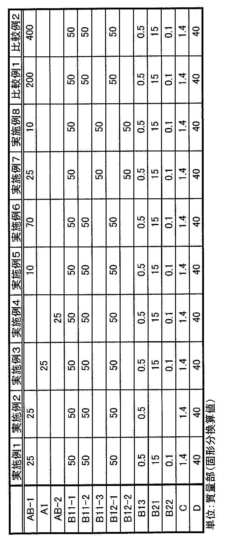
得られた接着シートの接着剤層(フィルム状接着剤)について、各評価を行った。結果を表2に示す。

Claims (7)
- 重合体成分(A)および熱硬化性成分(B1)を含むフィルム状接着剤であって、
該フィルム状接着剤における重合体成分(A)の含有率が1~30質量%、熱硬化性成分(B1)の含有率が40~70質量%であり、
複数のチップ体からなるチップ群に該フィルム状接着剤を貼付し、加熱気体を該フィルム状接着剤に向けて放出することにより該フィルム状接着剤を溶断することに用いられるフィルム状接着剤。 - 加熱硬化前の状態において、80℃における溶融粘度が1.0×10⁵Pa・s未満である請求項1に記載のフィルム状接着剤。
- 前記複数のチップ体からなるチップ群が、ワークの表面における領域であって、ワークを個片化した後にチップ体として残る領域以外の領域に溝を設け、ワークの裏面側から溝の底部に到るまでワークの薄化処理を行うことにより得られたものである請求項1または2に記載のフィルム状接着剤。
- 請求項1~3のいずれかに記載のフィルム状接着剤を接着剤層とし、該接着剤層が剥離可能に支持体に積層されている接着シート。
- 以下の(a)工程及び(b)工程を含む半導体装置の製造方法;
(a)重合体成分(A)及び熱硬化性成分(B1)を含み、重合体成分(A)の含有率が1~30質量%、熱硬化性成分(B1)の含有率が40~70質量%であるフィルム状接着剤を複数のチップ体からなるチップ群に貼付する工程、および
(b)加熱気体を該フィルム状接着剤に向けて放出することにより該フィルム状接着剤を溶断する工程。 - 加熱硬化前の状態での前記フィルム状接着剤の80℃における溶融粘度が、1.0×10⁵Pa・s未満である請求項5に記載の半導体装置の製造方法。
- さらに、前記(a)工程を行う前に、以下の(c)工程を含む請求項5または6に記載の半導体装置の製造方法;
(c)ワークの表面における領域であって、ワークを個片化した後にチップ体として残る領域以外の領域に溝を設け、ワークの裏面側から溝の底部に到るまでワークの薄化処理を行うことにより前記複数のチップ体からなるチップ群を得る工程。
Priority Applications (1)
| Application Number | Priority Date | Filing Date | Title |
|---|---|---|---|
| JP2017502406A JP6735270B2 (ja) | 2015-02-24 | 2016-02-24 | フィルム状接着剤、接着シートおよび半導体装置の製造方法 |
Applications Claiming Priority (2)
| Application Number | Priority Date | Filing Date | Title |
|---|---|---|---|
| JP2015-034170 | 2015-02-24 | ||
| JP2015034170 | 2015-02-24 |
Publications (1)
| Publication Number | Publication Date |
|---|---|
| WO2016136774A1 true WO2016136774A1 (ja) | 2016-09-01 |
Family
ID=56788671
Family Applications (1)
| Application Number | Title | Priority Date | Filing Date |
|---|---|---|---|
| PCT/JP2016/055344 Ceased WO2016136774A1 (ja) | 2015-02-24 | 2016-02-24 | フィルム状接着剤、接着シートおよび半導体装置の製造方法 |
Country Status (3)
| Country | Link |
|---|---|
| JP (2) | JP6735270B2 (ja) |
| TW (1) | TW201704395A (ja) |
| WO (1) | WO2016136774A1 (ja) |
Cited By (3)
| Publication number | Priority date | Publication date | Assignee | Title |
|---|---|---|---|---|
| WO2019189541A1 (ja) * | 2018-03-30 | 2019-10-03 | リンテック株式会社 | 樹脂シート、樹脂シートの使用方法、及び硬化樹脂層付き硬化封止体の製造方法 |
| WO2019230575A1 (ja) * | 2018-05-28 | 2019-12-05 | デンカ株式会社 | 粘着テープ及びそれを用いた半導体装置の製造方法 |
| CN113613893A (zh) * | 2019-03-15 | 2021-11-05 | 琳得科株式会社 | 粘合片及半导体装置的制造方法 |
Families Citing this family (2)
| Publication number | Priority date | Publication date | Assignee | Title |
|---|---|---|---|---|
| KR102401234B1 (ko) * | 2020-11-25 | 2022-05-24 | 에이엠씨주식회사 | 에너지선 경화형 화합물을 함유하는 점착시트 및 반도체 칩의 제조방법 |
| TWI879450B (zh) * | 2024-02-23 | 2025-04-01 | 翌驊實業股份有限公司 | 應用於sdbg製程之封裝貼合膜、其製備方法及其使用方法 |
Citations (4)
| Publication number | Priority date | Publication date | Assignee | Title |
|---|---|---|---|---|
| JP2006093213A (ja) * | 2004-09-21 | 2006-04-06 | Hitachi Chem Co Ltd | 接着剤層付き半導体素子の製造方法 |
| JP2008133456A (ja) * | 2006-10-24 | 2008-06-12 | Hitachi Chem Co Ltd | 半導体用接着剤組成物、半導体用接着シート及び半導体装置 |
| JP2008274259A (ja) * | 2007-04-02 | 2008-11-13 | Hitachi Chem Co Ltd | 接着シート |
| JP2012164953A (ja) * | 2011-01-21 | 2012-08-30 | Toshiba Corp | 半導体装置、並びに、その製造方法及び製造装置 |
Family Cites Families (1)
| Publication number | Priority date | Publication date | Assignee | Title |
|---|---|---|---|---|
| JP6133542B2 (ja) * | 2012-02-29 | 2017-05-24 | 日立化成株式会社 | フィルム状接着剤、接着シート及び半導体装置 |
-
2016
- 2016-02-24 TW TW105105383A patent/TW201704395A/zh unknown
- 2016-02-24 JP JP2017502406A patent/JP6735270B2/ja active Active
- 2016-02-24 WO PCT/JP2016/055344 patent/WO2016136774A1/ja not_active Ceased
-
2020
- 2020-01-30 JP JP2020013505A patent/JP6833083B2/ja active Active
Patent Citations (4)
| Publication number | Priority date | Publication date | Assignee | Title |
|---|---|---|---|---|
| JP2006093213A (ja) * | 2004-09-21 | 2006-04-06 | Hitachi Chem Co Ltd | 接着剤層付き半導体素子の製造方法 |
| JP2008133456A (ja) * | 2006-10-24 | 2008-06-12 | Hitachi Chem Co Ltd | 半導体用接着剤組成物、半導体用接着シート及び半導体装置 |
| JP2008274259A (ja) * | 2007-04-02 | 2008-11-13 | Hitachi Chem Co Ltd | 接着シート |
| JP2012164953A (ja) * | 2011-01-21 | 2012-08-30 | Toshiba Corp | 半導体装置、並びに、その製造方法及び製造装置 |
Cited By (10)
| Publication number | Priority date | Publication date | Assignee | Title |
|---|---|---|---|---|
| WO2019189541A1 (ja) * | 2018-03-30 | 2019-10-03 | リンテック株式会社 | 樹脂シート、樹脂シートの使用方法、及び硬化樹脂層付き硬化封止体の製造方法 |
| JPWO2019189541A1 (ja) * | 2018-03-30 | 2021-04-22 | リンテック株式会社 | 樹脂シート、樹脂シートの使用方法、及び硬化樹脂層付き硬化封止体の製造方法 |
| JP7280242B2 (ja) | 2018-03-30 | 2023-05-23 | リンテック株式会社 | 樹脂シート、樹脂シートの使用方法、及び硬化樹脂層付き硬化封止体の製造方法 |
| JP2023107769A (ja) * | 2018-03-30 | 2023-08-03 | リンテック株式会社 | 樹脂シート、樹脂シートの使用方法、及び硬化樹脂層付き硬化封止体の製造方法 |
| JP7651610B2 (ja) | 2018-03-30 | 2025-03-26 | リンテック株式会社 | 樹脂シート、樹脂シートの使用方法、及び硬化樹脂層付き硬化封止体の製造方法 |
| WO2019230575A1 (ja) * | 2018-05-28 | 2019-12-05 | デンカ株式会社 | 粘着テープ及びそれを用いた半導体装置の製造方法 |
| JPWO2019230575A1 (ja) * | 2018-05-28 | 2021-06-24 | デンカ株式会社 | 粘着テープ及びそれを用いた半導体装置の製造方法 |
| JP7304345B2 (ja) | 2018-05-28 | 2023-07-06 | デンカ株式会社 | 粘着テープ及びそれを用いた半導体装置の製造方法 |
| CN113613893A (zh) * | 2019-03-15 | 2021-11-05 | 琳得科株式会社 | 粘合片及半导体装置的制造方法 |
| CN113613893B (zh) * | 2019-03-15 | 2023-11-21 | 琳得科株式会社 | 粘合片及半导体装置的制造方法 |
Also Published As
| Publication number | Publication date |
|---|---|
| JP6833083B2 (ja) | 2021-02-24 |
| JP6735270B2 (ja) | 2020-08-05 |
| TW201704395A (zh) | 2017-02-01 |
| JP2020098918A (ja) | 2020-06-25 |
| JPWO2016136774A1 (ja) | 2017-11-30 |
Similar Documents
| Publication | Publication Date | Title |
|---|---|---|
| KR101634064B1 (ko) | 수지막 형성용 복합 시트 | |
| JP6336905B2 (ja) | フィルム状接着剤、半導体接合用接着シート、および半導体装置の製造方法 | |
| JP5684948B2 (ja) | 接着性樹脂層付シートおよび半導体装置の製造方法 | |
| JP5917215B2 (ja) | 接着剤組成物、接着シートおよび半導体装置の製造方法 | |
| JP6833083B2 (ja) | フィルム状接着剤、接着シートおよび半導体装置の製造方法 | |
| JP6250265B2 (ja) | 接着剤組成物、接着シートおよび半導体装置の製造方法 | |
| JP5774322B2 (ja) | 半導体用接着剤組成物、半導体用接着シートおよび半導体装置の製造方法 | |
| JP6437431B2 (ja) | 半導体チップの製造方法 | |
| JP6393449B2 (ja) | 接着剤組成物、接着シートおよび半導体装置の製造方法 | |
| JPWO2014155756A1 (ja) | 粘着シートおよび保護膜形成用複合シートならびに保護膜付きチップの製造方法 | |
| JP5887029B1 (ja) | ダイボンド層形成フィルム、ダイボンド層形成フィルムが付着した加工物、および半導体装置 | |
| JP2012167174A (ja) | 接着剤組成物、接着シートおよび半導体装置の製造方法 | |
| JP6369996B2 (ja) | 樹脂膜形成用シート | |
| JP6262717B2 (ja) | 保護膜付チップの製造方法 | |
| JP6574787B2 (ja) | 樹脂膜形成用シート積層体 | |
| WO2013157567A1 (ja) | 接着剤組成物、接着シートおよび半導体装置の製造方法 | |
| JP5005258B2 (ja) | 粘接着剤組成物、粘接着シートおよび半導体装置の製造方法 | |
| JP6279319B2 (ja) | 樹脂膜形成用複合シート | |
| JP2014192463A (ja) | 樹脂膜形成用シート | |
| JP5727811B2 (ja) | 半導体チップのピックアップ方法および半導体装置の製造方法 | |
| JP5951206B2 (ja) | ダイシング・ダイボンディングシート | |
| JP2014192462A (ja) | 樹脂膜形成用シート |
Legal Events
| Date | Code | Title | Description |
|---|---|---|---|
| 121 | Ep: the epo has been informed by wipo that ep was designated in this application |
Ref document number: 16755518 Country of ref document: EP Kind code of ref document: A1 |
|
| ENP | Entry into the national phase |
Ref document number: 2017502406 Country of ref document: JP Kind code of ref document: A |
|
| NENP | Non-entry into the national phase |
Ref country code: DE |
|
| 122 | Ep: pct application non-entry in european phase |
Ref document number: 16755518 Country of ref document: EP Kind code of ref document: A1 |