WO2016136516A1 - インバータ装置 - Google Patents
インバータ装置 Download PDFInfo
- Publication number
- WO2016136516A1 WO2016136516A1 PCT/JP2016/054273 JP2016054273W WO2016136516A1 WO 2016136516 A1 WO2016136516 A1 WO 2016136516A1 JP 2016054273 W JP2016054273 W JP 2016054273W WO 2016136516 A1 WO2016136516 A1 WO 2016136516A1
- Authority
- WO
- WIPO (PCT)
- Prior art keywords
- semiconductor power
- positive
- conductors
- power modules
- connection
- Prior art date
- Legal status (The legal status is an assumption and is not a legal conclusion. Google has not performed a legal analysis and makes no representation as to the accuracy of the status listed.)
- Ceased
Links
Images

Classifications
-
- H—ELECTRICITY
- H02—GENERATION; CONVERSION OR DISTRIBUTION OF ELECTRIC POWER
- H02M—APPARATUS FOR CONVERSION BETWEEN AC AND AC, BETWEEN AC AND DC, OR BETWEEN DC AND DC, AND FOR USE WITH MAINS OR SIMILAR POWER SUPPLY SYSTEMS; CONVERSION OF DC OR AC INPUT POWER INTO SURGE OUTPUT POWER; CONTROL OR REGULATION THEREOF
- H02M7/00—Conversion of AC power input into DC power output; Conversion of DC power input into AC power output
- H02M7/003—Constructional details, e.g. physical layout, assembly, wiring or busbar connections
-
- H—ELECTRICITY
- H02—GENERATION; CONVERSION OR DISTRIBUTION OF ELECTRIC POWER
- H02M—APPARATUS FOR CONVERSION BETWEEN AC AND AC, BETWEEN AC AND DC, OR BETWEEN DC AND DC, AND FOR USE WITH MAINS OR SIMILAR POWER SUPPLY SYSTEMS; CONVERSION OF DC OR AC INPUT POWER INTO SURGE OUTPUT POWER; CONTROL OR REGULATION THEREOF
- H02M7/00—Conversion of AC power input into DC power output; Conversion of DC power input into AC power output
- H02M7/42—Conversion of DC power input into AC power output without possibility of reversal
- H02M7/44—Conversion of DC power input into AC power output without possibility of reversal by static converters
- H02M7/48—Conversion of DC power input into AC power output without possibility of reversal by static converters using discharge tubes with control electrode or semiconductor devices with control electrode
-
- H—ELECTRICITY
- H05—ELECTRIC TECHNIQUES NOT OTHERWISE PROVIDED FOR
- H05K—PRINTED CIRCUITS; CASINGS OR CONSTRUCTIONAL DETAILS OF ELECTRIC APPARATUS; MANUFACTURE OF ASSEMBLAGES OF ELECTRICAL COMPONENTS
- H05K7/00—Constructional details common to different types of electric apparatus
- H05K7/14—Mounting supporting structure in casing or on frame or rack
- H05K7/1422—Printed circuit boards receptacles, e.g. stacked structures, electronic circuit modules or box like frames
- H05K7/1427—Housings
- H05K7/1432—Housings specially adapted for power drive units or power converters
- H05K7/14329—Housings specially adapted for power drive units or power converters specially adapted for the configuration of power bus bars
-
- H—ELECTRICITY
- H05—ELECTRIC TECHNIQUES NOT OTHERWISE PROVIDED FOR
- H05K—PRINTED CIRCUITS; CASINGS OR CONSTRUCTIONAL DETAILS OF ELECTRIC APPARATUS; MANUFACTURE OF ASSEMBLAGES OF ELECTRICAL COMPONENTS
- H05K7/00—Constructional details common to different types of electric apparatus
- H05K7/20—Modifications to facilitate cooling, ventilating, or heating
- H05K7/2089—Modifications to facilitate cooling, ventilating, or heating for power electronics, e.g. for inverters for controlling motor
- H05K7/209—Heat transfer by conduction from internal heat source to heat radiating structure
Definitions
- the present invention relates to an inverter device, and more particularly to a member arrangement of the inverter device with reduced circuit inductance.
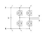
- IGBT semiconductor power modules for each phase
- IGBT1 to IGBT4 a plurality of semiconductor power modules for each phase
- a smoothing capacitor C a connection conductor for a DC circuit P, N and output conductors (output terminals) U, V are mainly configured.
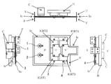
- the arrangement structure of each member in this apparatus is generally configured as shown in FIG.
- IGBT1 and IGBT2 connected in series that become U-phase arms are arranged in the front-rear direction (vertical direction in the plan view), and IGBT3 and IGBT4 that are connected in series adjacent to each other in parallel are V-phase arms.
- the connecting conductors P and N are led out in the left direction in the drawing and bent in a right angle direction, and the output conductors U and V are led out in the right direction in the drawing.
- the smoothing capacitor C is disposed between the IGBT and the bent connection conductors P and N.
- In is an insulating member
- H is a heat sink.
- Patent Document 1 and Patent Document 2 are publicly known as inverter devices with reduced circuit inductance. JP 2013-42663 JP 2006-262623 A
- the distance to the fixing member 4, that is, the IGBT 3 is longer, and the distance between the IGBT 1 and the IGBT 3 connected between the same connection conductors P is uneven. For this reason, the loop of the current flowing between the capacitor C and the IGBTs 1 and 2 at the time of switching and the loop of the current flowing between the capacitor C and the IGBTs 3 and 4 are imbalanced and cause circuit inductance.
- the inductance between the IGBT output and the load end is reduced to reduce the circuit loop as the device, or the conductors in the current direction facing each other are aligned. It is an essential task to reduce the inductance of the circuit by arranging them.
- an object of the present invention is to provide an inverter device having a reduced circuit inductance.
- a plurality of semiconductor power modules for each phase to which a heat sink is attached, positive and negative connection conductors for a DC circuit, smoothing capacitors, and output conductors for each phase are mainly used.
- the semiconductor power module connected to the positive connection conductor and the semiconductor power module connected to the negative connection conductor in the state where the semiconductor power modules connected in series are overlapped, and the same for each polarity.
- the positive and negative connection conductors are arranged through the gap to the vicinity of the connection terminals of the semiconductor power module in a state parallel to the insulating member,
- the smoothing capacitor is attached to a portion arranged in parallel with an insulating member interposed therebetween,
- the output conductor from the semiconductor power module is derived in parallel with an insulating member interposed between the phases.
- the smoothing capacitors of the present invention are arranged in a staggered manner on the positive and negative connection conductors.
- connection conductors of the present invention are formed of plate-like conductors and bent at approximately 90 degrees in the vicinity of the connection terminal portion of the semiconductor power module.
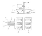
- the block diagram of the inverter apparatus which shows embodiment of this invention.
- the circuit diagram of a single phase inverter The block diagram of the conventional single phase inverter apparatus.
- FIG. 1 is a configuration diagram of member arrangement according to the present invention and shows an example of a single-phase inverter device.
- the U-phase arm and the V-phase arm are arranged in an overlapped manner, and the IGBTs connected in series in each phase are arranged in the drawing depth direction with the heat sink H attached.
- the IGBTs 1 and 3 (in FIG. 3) connected to the positive connection conductor P and the IGBTs 2 and 4 connected to the negative connection conductor N have a left and right side as shown in the plan view.
- the connecting conductors P and N are extended in parallel with the insulating member In interposed in the center of the interval.
- a plurality of smoothing capacitors C are provided on one or both sides of the extended connection conductors P and N, and the positive and negative terminals of the smoothing capacitor C are connected to the connection conductors P and N, respectively.
- the number of smoothing capacitors C is increased and provided on both sides of the connection conductors P and N, they are arranged in a staggered manner on the left and right sides so as not to interfere with the attachment of the smoothing capacitors C.
- connection conductors P and N are made of a plate-like member, and extends to the vicinity of the connection terminal portion of each IGBT in parallel with the plate-like insulating member In between them.
- the negative electrode is bent by about 90 degrees to the left and right, and the positive and negative terminals of each IGBT are connected.
- the U-phase and V-phase output conductors U and V are also stretched from the front side of the front view with the insulating member In interposed therebetween, and are divided into left and right in the vicinity of the connection terminal portion of the IGBT.
- the output conductors U and V are connected to the connection conductors P and N so as to be orthogonal to each other and connected to the terminal on the AC output side of each IGBT.
- the smoothing capacitor C is disposed on the rear side of the heat sink H so that it does not hinder the screwing of the terminal portion of the IGBT.
- FIG. 2 shows a schematic diagram of a three-phase inverter device.
- the IGBTs 1, 3, 5 connected to the connection conductor P are arranged on the right side of the drawing, and the IGBTs 2, 4, 6 connected to the connection conductor N are shown in FIG. Is arranged on the right side of the drawing.
- the reactance from the inverter output to the load end is slightly larger in the U and W phases than in the V phase compared to the single layer inverter, but the circuit inductance is sufficiently reduced compared to the conventional one. Is possible.
- the group of IGBTs connected to the positive connection conductor P and the group of IGBTs connected to the negative connection conductor N are equidistant along the connection conductors P and N, respectively. Placed in. As a result, the current flowing between the smoothing capacitor C and IGBT1 and IGBT2 during switching and the circuit loop of the smoothing capacitor C and IGBT3 and IGBT4 become smaller, and the flowing current balances and cancels the circuit inductance, thereby reducing circuit inductance. Is possible.
Landscapes
- Engineering & Computer Science (AREA)
- Microelectronics & Electronic Packaging (AREA)
- Power Engineering (AREA)
- Physics & Mathematics (AREA)
- Thermal Sciences (AREA)
- Inverter Devices (AREA)
Abstract
Description
また、平滑コンデンサCは、IGBTと屈曲された接続導体P,N間に配置されている。Inは絶縁部材、Hはヒートシンクである。
(1)電流の導通経路が屈折するため回路ループが大きくなり、回路のインダクタンスが増える。
(2)対向する電流方向の導体を沿わせて配置することで回路インダクタンスを打ち消し合うことは周知であるが、実際には接続導体が分岐するため電流方向の導体を沿わせて配置することが難しい。
前記半導体パワーモジュールを直列に接続した相毎のアームを重ねた状態で、且つ正極用の接続導体に接続される半導体パワーモジュールと負極用の接続導体に接続される半導体パワーモジュールを極性毎に同一方向に配列してその極性間に間隙を設け、
前記正、負極用の接続導体は、絶縁部材を挟んで並行した状態で半導体パワーモジュールの接続端子付近まで前記間隙を通して配設し、
前記平滑コンデンサは、絶縁部材を挟んで並行配設された部分に取り付け、
前記半導体パワーモジュールからの出力導体は、各相間に絶縁部材を挟んで並行に導出したものである。
Claims (3)
- ヒートシンクを取付けた相毎の複数の半導体パワーモジュールと、直流回路の正,負極用の接続導体と、平滑コンデンサ及び相毎の出力導体の各部材を主体として構成されるインバータ装置の配置において、
前記半導体パワーモジュールを直列に接続した相毎のアームを重ねた状態で、且つ正極用の接続導体に接続される半導体パワーモジュールと負極用の接続導体に接続される半導体パワーモジュールを極性毎に同一方向に配列してその極性間に間隙を設け、
前記正、負極用の接続導体は、絶縁部材を挟んで並行した状態で半導体パワーモジュールの接続端子付近まで前記間隙を通して配設し、
前記平滑コンデンサは、絶縁部材を挟んで並行配設された部分に取り付け、
前記半導体パワーモジュールからの出力導体は、各相間に絶縁部材を挟んで並行に導出して構成することを特徴としたインバータ装置。 - 前記平滑コンデンサは、正、負極用の接続導体に互いに千鳥状に配置したことを特徴とした請求項1記載のインバータ装置。
- 前記正、負極用の接続導体は、板状の導体で形成され、前記半導体パワーモジュールの接続端子部近辺で略90度に屈曲されたことを特徴とした請求項1又は2記載のインバータ装置。
Priority Applications (2)
| Application Number | Priority Date | Filing Date | Title |
|---|---|---|---|
| RU2017120522A RU2653359C1 (ru) | 2015-02-24 | 2016-02-15 | Инверторное устройство |
| US15/552,935 US9954459B2 (en) | 2015-02-24 | 2016-02-15 | Inverter device |
Applications Claiming Priority (2)
| Application Number | Priority Date | Filing Date | Title |
|---|---|---|---|
| JP2015-033457 | 2015-02-24 | ||
| JP2015033457A JP6011656B2 (ja) | 2015-02-24 | 2015-02-24 | インバータ装置 |
Publications (1)
| Publication Number | Publication Date |
|---|---|
| WO2016136516A1 true WO2016136516A1 (ja) | 2016-09-01 |
Family
ID=56788383
Family Applications (1)
| Application Number | Title | Priority Date | Filing Date |
|---|---|---|---|
| PCT/JP2016/054273 Ceased WO2016136516A1 (ja) | 2015-02-24 | 2016-02-15 | インバータ装置 |
Country Status (4)
| Country | Link |
|---|---|
| US (1) | US9954459B2 (ja) |
| JP (1) | JP6011656B2 (ja) |
| RU (1) | RU2653359C1 (ja) |
| WO (1) | WO2016136516A1 (ja) |
Families Citing this family (2)
| Publication number | Priority date | Publication date | Assignee | Title |
|---|---|---|---|---|
| CA3067320C (en) * | 2017-06-15 | 2020-06-23 | Nissan Motor Co., Ltd. | Power conversion device |
| JP7088106B2 (ja) * | 2019-03-28 | 2022-06-21 | 株式会社明電舎 | 導体接続構造 |
Citations (9)
| Publication number | Priority date | Publication date | Assignee | Title |
|---|---|---|---|---|
| JPH07298641A (ja) * | 1994-03-04 | 1995-11-10 | Nippondenso Co Ltd | インバータ装置 |
| JPH08510112A (ja) * | 1993-09-22 | 1996-10-22 | ハネウエル アクチエンゲゼルシャフト | 電力変換装置 |
| EP0766504A2 (en) * | 1995-09-29 | 1997-04-02 | Allen-Bradley Company, Inc. | A wireless circuit board system for a motor controller |
| JPH09308267A (ja) * | 1996-05-13 | 1997-11-28 | Nippon Soken Inc | バスバーとコンデンサの組付け構造 |
| US5835362A (en) * | 1995-04-07 | 1998-11-10 | Asea Brown Boveri Ag | Current conductor arrangement |
| JP2002044949A (ja) * | 2000-07-21 | 2002-02-08 | Yaskawa Electric Corp | インバータの平滑コンデンサの配列方法 |
| JP2004056984A (ja) * | 2002-07-24 | 2004-02-19 | Mitsubishi Electric Corp | 電力変換装置 |
| JP2006310490A (ja) * | 2005-04-27 | 2006-11-09 | Toyota Industries Corp | コンデンサ装置 |
| JP2011172469A (ja) * | 2010-01-22 | 2011-09-01 | Denso Corp | 電力変換装置 |
Family Cites Families (9)
| Publication number | Priority date | Publication date | Assignee | Title |
|---|---|---|---|---|
| JP3225457B2 (ja) * | 1995-02-28 | 2001-11-05 | 株式会社日立製作所 | 半導体装置 |
| DE19756250C2 (de) * | 1997-12-17 | 2000-11-02 | Siemens Ag | Selbstgeführter Stromrichter eines spannungseinprägenden Umrichters mit Hochleistungs-Modulen |
| JP3793407B2 (ja) * | 2000-09-19 | 2006-07-05 | 株式会社日立製作所 | 電力変換装置 |
| JP3563038B2 (ja) * | 2001-03-05 | 2004-09-08 | 東芝トランスポートエンジニアリング株式会社 | 電力変換装置 |
| JP2006262623A (ja) | 2005-03-17 | 2006-09-28 | Toshiba Mitsubishi-Electric Industrial System Corp | 電力変換ユニットおよび電力変換装置 |
| US7892670B2 (en) * | 2005-08-31 | 2011-02-22 | Siemens Industry, Inc. | Packaging system for modular power cells |
| US9041183B2 (en) * | 2011-07-19 | 2015-05-26 | Ut-Battelle, Llc | Power module packaging with double sided planar interconnection and heat exchangers |
| JP5835167B2 (ja) * | 2012-09-07 | 2015-12-24 | トヨタ自動車株式会社 | パワーモジュール構造 |
| JP5557891B2 (ja) | 2012-11-30 | 2014-07-23 | 株式会社日立製作所 | 三相電力変換装置 |
-
2015
- 2015-02-24 JP JP2015033457A patent/JP6011656B2/ja not_active Expired - Fee Related
-
2016
- 2016-02-15 RU RU2017120522A patent/RU2653359C1/ru active
- 2016-02-15 WO PCT/JP2016/054273 patent/WO2016136516A1/ja not_active Ceased
- 2016-02-15 US US15/552,935 patent/US9954459B2/en not_active Expired - Fee Related
Patent Citations (9)
| Publication number | Priority date | Publication date | Assignee | Title |
|---|---|---|---|---|
| JPH08510112A (ja) * | 1993-09-22 | 1996-10-22 | ハネウエル アクチエンゲゼルシャフト | 電力変換装置 |
| JPH07298641A (ja) * | 1994-03-04 | 1995-11-10 | Nippondenso Co Ltd | インバータ装置 |
| US5835362A (en) * | 1995-04-07 | 1998-11-10 | Asea Brown Boveri Ag | Current conductor arrangement |
| EP0766504A2 (en) * | 1995-09-29 | 1997-04-02 | Allen-Bradley Company, Inc. | A wireless circuit board system for a motor controller |
| JPH09308267A (ja) * | 1996-05-13 | 1997-11-28 | Nippon Soken Inc | バスバーとコンデンサの組付け構造 |
| JP2002044949A (ja) * | 2000-07-21 | 2002-02-08 | Yaskawa Electric Corp | インバータの平滑コンデンサの配列方法 |
| JP2004056984A (ja) * | 2002-07-24 | 2004-02-19 | Mitsubishi Electric Corp | 電力変換装置 |
| JP2006310490A (ja) * | 2005-04-27 | 2006-11-09 | Toyota Industries Corp | コンデンサ装置 |
| JP2011172469A (ja) * | 2010-01-22 | 2011-09-01 | Denso Corp | 電力変換装置 |
Also Published As
| Publication number | Publication date |
|---|---|
| JP6011656B2 (ja) | 2016-10-19 |
| US9954459B2 (en) | 2018-04-24 |
| RU2653359C1 (ru) | 2018-05-08 |
| US20180054137A1 (en) | 2018-02-22 |
| JP2016158342A (ja) | 2016-09-01 |
Similar Documents
| Publication | Publication Date | Title |
|---|---|---|
| US10153708B2 (en) | Three-level power converter | |
| JP5533068B2 (ja) | 半導体装置 | |
| US9425701B2 (en) | Power conversion device | |
| JP2014533487A (ja) | Hブリッジに基づく電力変換器 | |
| JP5476510B2 (ja) | 電力変換装置 | |
| US9641092B2 (en) | Power converter | |
| JP5420122B2 (ja) | 電力変換装置 | |
| CN108377667B (zh) | 用于互连并联的igbt模块的方法和系统 | |
| EP2717454B1 (en) | Power conversion device | |
| JPH07111310A (ja) | 半導体装置 | |
| CN105024532A (zh) | 一种单相三电平逆变器及三相三电平逆变器 | |
| CN103563230A (zh) | 电力变换装置 | |
| JPWO2015133024A1 (ja) | 電力用半導体装置 | |
| US9490721B2 (en) | Power conversion device | |
| JP2004135444A (ja) | 電力変換装置のスタック構造 | |
| JP6011656B2 (ja) | インバータ装置 | |
| JP5599757B2 (ja) | 電力変換装置 | |
| JP5678597B2 (ja) | 電力変換器の主回路構造 | |
| JP2017005212A (ja) | パワー半導体回路及びパワー半導体素子の実装方法 | |
| JP6604097B2 (ja) | スイッチング回路および電力変換装置 | |
| JP6362959B2 (ja) | 電力変換回路、その製造方法、および、パワーコンディショナ | |
| JP6844932B2 (ja) | 電力変換装置 | |
| JP2017188996A (ja) | インバータ装置 | |
| JP5950800B2 (ja) | 電力変換装置 | |
| JPWO2015019480A1 (ja) | 電力変換装置 |
Legal Events
| Date | Code | Title | Description |
|---|---|---|---|
| 121 | Ep: the epo has been informed by wipo that ep was designated in this application |
Ref document number: 16755263 Country of ref document: EP Kind code of ref document: A1 |
|
| WWE | Wipo information: entry into national phase |
Ref document number: 15552935 Country of ref document: US |
|
| NENP | Non-entry into the national phase |
Ref country code: DE |
|
| ENP | Entry into the national phase |
Ref document number: 2017120522 Country of ref document: RU Kind code of ref document: A |
|
| 122 | Ep: pct application non-entry in european phase |
Ref document number: 16755263 Country of ref document: EP Kind code of ref document: A1 |