WO2016132850A1 - 遮光体を含む光学装置の製造方法、および記憶媒体 - Google Patents
遮光体を含む光学装置の製造方法、および記憶媒体 Download PDFInfo
- Publication number
- WO2016132850A1 WO2016132850A1 PCT/JP2016/052550 JP2016052550W WO2016132850A1 WO 2016132850 A1 WO2016132850 A1 WO 2016132850A1 JP 2016052550 W JP2016052550 W JP 2016052550W WO 2016132850 A1 WO2016132850 A1 WO 2016132850A1
- Authority
- WO
- WIPO (PCT)
- Prior art keywords
- substrate
- optical device
- plating
- plating layer
- catalyst adsorption
- Prior art date
- Legal status (The legal status is an assumption and is not a legal conclusion. Google has not performed a legal analysis and makes no representation as to the accuracy of the status listed.)
- Ceased
Links
Images






Classifications
-
- H—ELECTRICITY
- H10—SEMICONDUCTOR DEVICES; ELECTRIC SOLID-STATE DEVICES NOT OTHERWISE PROVIDED FOR
- H10F—INORGANIC SEMICONDUCTOR DEVICES SENSITIVE TO INFRARED RADIATION, LIGHT, ELECTROMAGNETIC RADIATION OF SHORTER WAVELENGTH OR CORPUSCULAR RADIATION
- H10F39/00—Integrated devices, or assemblies of multiple devices, comprising at least one element covered by group H10F30/00, e.g. radiation detectors comprising photodiode arrays
- H10F39/011—Manufacture or treatment of image sensors covered by group H10F39/12
-
- C—CHEMISTRY; METALLURGY
- C23—COATING METALLIC MATERIAL; COATING MATERIAL WITH METALLIC MATERIAL; CHEMICAL SURFACE TREATMENT; DIFFUSION TREATMENT OF METALLIC MATERIAL; COATING BY VACUUM EVAPORATION, BY SPUTTERING, BY ION IMPLANTATION OR BY CHEMICAL VAPOUR DEPOSITION, IN GENERAL; INHIBITING CORROSION OF METALLIC MATERIAL OR INCRUSTATION IN GENERAL
- C23C—COATING METALLIC MATERIAL; COATING MATERIAL WITH METALLIC MATERIAL; SURFACE TREATMENT OF METALLIC MATERIAL BY DIFFUSION INTO THE SURFACE, BY CHEMICAL CONVERSION OR SUBSTITUTION; COATING BY VACUUM EVAPORATION, BY SPUTTERING, BY ION IMPLANTATION OR BY CHEMICAL VAPOUR DEPOSITION, IN GENERAL
- C23C18/00—Chemical coating by decomposition of either liquid compounds or solutions of the coating forming compounds, without leaving reaction products of surface material in the coating; Contact plating
- C23C18/16—Chemical coating by decomposition of either liquid compounds or solutions of the coating forming compounds, without leaving reaction products of surface material in the coating; Contact plating by reduction or substitution, e.g. electroless plating
- C23C18/31—Coating with metals
- C23C18/32—Coating with nickel, cobalt or mixtures thereof with phosphorus or boron
-
- G—PHYSICS
- G02—OPTICS
- G02B—OPTICAL ELEMENTS, SYSTEMS OR APPARATUS
- G02B5/00—Optical elements other than lenses
- G02B5/20—Filters
-
- H—ELECTRICITY
- H10—SEMICONDUCTOR DEVICES; ELECTRIC SOLID-STATE DEVICES NOT OTHERWISE PROVIDED FOR
- H10F—INORGANIC SEMICONDUCTOR DEVICES SENSITIVE TO INFRARED RADIATION, LIGHT, ELECTROMAGNETIC RADIATION OF SHORTER WAVELENGTH OR CORPUSCULAR RADIATION
- H10F39/00—Integrated devices, or assemblies of multiple devices, comprising at least one element covered by group H10F30/00, e.g. radiation detectors comprising photodiode arrays
- H10F39/80—Constructional details of image sensors
- H10F39/805—Coatings
- H10F39/8057—Optical shielding
-
- H—ELECTRICITY
- H10—SEMICONDUCTOR DEVICES; ELECTRIC SOLID-STATE DEVICES NOT OTHERWISE PROVIDED FOR
- H10F—INORGANIC SEMICONDUCTOR DEVICES SENSITIVE TO INFRARED RADIATION, LIGHT, ELECTROMAGNETIC RADIATION OF SHORTER WAVELENGTH OR CORPUSCULAR RADIATION
- H10F99/00—Subject matter not provided for in other groups of this subclass
-
- H—ELECTRICITY
- H10—SEMICONDUCTOR DEVICES; ELECTRIC SOLID-STATE DEVICES NOT OTHERWISE PROVIDED FOR
- H10P—GENERIC PROCESSES OR APPARATUS FOR THE MANUFACTURE OR TREATMENT OF DEVICES COVERED BY CLASS H10
- H10P14/00—Formation of materials, e.g. in the shape of layers or pillars
- H10P14/40—Formation of materials, e.g. in the shape of layers or pillars of conductive or resistive materials
- H10P14/46—Formation of materials, e.g. in the shape of layers or pillars of conductive or resistive materials using a liquid
Definitions
- the present invention relates to a method for manufacturing an optical device including a light shield, a manufacturing system thereof, and a storage medium, and more particularly, to a method for manufacturing an optical device including a light shield that can be manufactured with high accuracy and low cost, and a storage medium. .
- Solid-state imaging devices such as a CMOS image sensor and a CCD image sensor include a front side irradiation type and a back side irradiation type.
- the back-illuminated solid-state imaging device has a large number of photodiodes provided on the front side of the semiconductor substrate, color filters and micro lenses are formed on the back side, and is generated by light incident on the semiconductor substrate from the back side.
- the photoelectric charge is read by a photodiode on the surface side, and the signal readout circuit outputs this photoelectric charge.
- This backside illumination type can provide a large aperture ratio because it is not necessary to provide a signal readout circuit on the backside, and the semiconductor substrate can be made thick so that almost all incident light energy can be photoelectrically converted.
- the back-illuminated solid-state imaging device has a problem that incident light incident obliquely enters an adjacent photodiode because the semiconductor substrate is thick and the optical path length is long in order to increase the photoelectric conversion efficiency.
- a light shielding body is formed on the semiconductor substrate by PVD or CVD so as to correspond to each photodiode.
- the present invention has been made in consideration of the above points, and has a method for manufacturing an optical device including a light-blocking body that can be manufactured with high accuracy and good light-blocking characteristics at low cost, and a storage medium.
- the purpose is to provide.
- the present invention provides a method for manufacturing an optical device including a light shielding body, and a step of preparing a substrate, and a plating solution containing Co or a Co alloy is supplied to the substrate to perform an electroless plating process. And a step of forming a Co or Co alloy plating layer to be a manufacturing method of an optical device including a light shielding body.
- the present invention relates to a storage medium storing a computer program for causing an optical device manufacturing system including a light shield to execute an optical device manufacturing method.
- the optical device manufacturing method includes: a step of preparing a substrate; And a step of forming a Co or Co alloy plating layer to be the light-shielding body by supplying a plating solution containing Co or a Co alloy to the electroless plating process. It is.
- a light shielding body can be produced with high accuracy and at low cost.
- FIG. 1 is a block diagram showing an optical device manufacturing system according to an embodiment of the present invention.
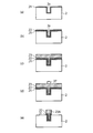
- FIGS. 2A to 2E are diagrams showing a substrate on which a method for manufacturing an optical device according to an embodiment of the present invention is applied.
- FIG. 3 is a diagram illustrating a solid-state imaging device showing an example of an optical device including a light shielding body.
- FIG. 4 is a diagram showing the light shielding characteristics of the light shielding body.
- FIG. 5 is a diagram illustrating the light blocking characteristics of the light blocking body.
- FIG. 6 is a diagram illustrating the light blocking characteristics of the light blocking body.
- FIG. 7 is a diagram showing the arrangement relationship between the photodiode and the light shielding member.
- FIG. 1 is a block diagram showing an optical device manufacturing system according to an embodiment of the present invention.
- FIGS. 2A to 2E are diagrams showing a substrate on which a method for manufacturing an optical device according to an embodiment of the present invention is applied.
- FIG. 3 is
- FIGS. 8A to 10E are diagrams showing a substrate on which a method for manufacturing an optical device according to a modification of the present invention is applied.
- FIGS. 11A to 11C are diagrams showing a substrate on which a method for manufacturing an optical device according to a modification of the present invention is applied.
- an optical device including a light blocking body for example, a back-illuminated solid-state imaging device 30 will be described with reference to FIG.
- the solid-state imaging device 30 is an interline CCD, and a plurality of vertical charge transfer paths (VCCD) 35 and a plurality of photodiodes (photoelectric conversion) constituting pixels on the surface side of the p-type semiconductor substrate 2.
- Element) 36 is formed, and a plurality of color filter (red (R), green (G), blue (B)) layers 33 and a plurality of microlenses 34 are provided on the back surface side.
- the color filter layers 33 of the respective colors are stacked at positions aligned with the corresponding photodiodes 36, and each microlens 34 is formed so as to be focused on the center of the corresponding photodiode 36.
- an insulating layer 37 and a metal electrode 38 are stacked on the vertical charge transfer path 35.
- Patent Document 3 is a CCD type, but for example, the present embodiment can be similarly applied to a CMOS type or other type of solid-state image sensor as in Patent Document 2.
- a recess 2 a is formed on the rear surface of the semiconductor substrate (hereinafter also referred to as a substrate) 2, and a color filter layer 33 and a microlens 34 are sequentially stacked on the rear surface of the substrate 2.
- the color filter layer 33 is partitioned in units of pixels (photodiodes) 36, and a light shielding body 23A is provided between adjacent partitions of the color filter layer 33 on the substrate 2 side.
- the light shield 23A is provided to prevent obliquely incident light from entering adjacent pixels.
- FIG. 7 is a diagram showing a state in which the light shielding body 23A is viewed from the back side, and is formed in a net shape as a whole, and each mesh section defines one pixel and one pixel.
- a manufacturing system 10 for an optical device including a light shielding body performs a plating process on a substrate (silicon substrate) 2 having a recess 2a such as a semiconductor wafer to produce a light shielding body.
- the optical apparatus manufacturing system 10 including such a light shielding body takes out the substrate 2 from the cassette station 18 on which a cassette (not shown) containing the substrate 2 is placed and transports the substrate 2 from the cassette on the cassette station 18.
- a substrate transport arm 11 and a travel path 11a along which the substrate transport arm 11 travels are provided.
- a catalyst adsorption layer forming portion 13 for adsorbing a catalyst on the substrate 2 to form a catalyst adsorption layer 22 described later, and Co or a Co alloy on the catalyst adsorption layer 22 of the substrate 2 are included.
- a plating layer forming unit 14 for forming a Co or Co alloy plating layer 23 is provided by supplying a plating solution and performing an electroless plating process.
- a baking portion 15 for baking the catalyst adsorption layer 22 and the plating layer 23 formed on the substrate 2 and a resist pattern forming portion 16 for forming a resist pattern 27 on the plating layer 23. And are arranged.
- the resist pattern forming portion 16 has a resist coating portion, an exposure portion, and a developing portion, although none of them is shown.
- an etching processing unit 17 that forms a light shielding body 23A that protrudes outward from the substrate 2 in the recess 2a of the substrate 2 by etching the plating layer 23 using the resist pattern 27 as a mask adjacent to the baking portion 15;
- a resist pattern removing portion 17A for removing the resist pattern 27 is disposed.
- each component of the plating processing system described above for example, the cassette station 18, the substrate transfer arm 11, the catalyst adsorption layer forming unit 13, the plating layer forming unit 14, the baking unit 15, the resist pattern forming unit 16, the etching processing unit 17, and the like.
- the resist pattern removing unit 17A is driven and controlled by the control unit 19 in accordance with various programs recorded in the storage medium 19A provided in the control unit 19, whereby various processes for the substrate 2 are performed.
- the storage medium 19A stores various programs such as various setting data and a plating program described later.
- known media such as a computer-readable memory such as ROM and RAM, and a disk-shaped storage medium such as a hard disk, CD-ROM, DVD-ROM, and flexible disk can be used.
- the plating layer forming unit 14 can be configured from a plating apparatus shown in FIGS. 8 and 9.
- Such a plating layer forming portion 14 is as shown in FIGS.
- the plating layer forming unit 14 is configured to plate the substrate rotation holding mechanism (substrate housing unit) 110 for rotating and holding the substrate 2 inside the casing 101 and the surface of the substrate 2.
- Liquid supply mechanisms 50 and 90 for supplying a liquid and a cleaning liquid, a cup 105 for receiving a plating liquid and a cleaning liquid scattered from the substrate 2, and outlets 124, 129 and 134 for discharging the plating liquid and the cleaning liquid received by the cup 105.
- the liquid discharge mechanism 120, 125, 130 for discharging the liquid collected at the discharge port, the substrate rotation holding mechanism 110, the liquid supply mechanism 50, 90, the cup 105, and the liquid discharge mechanism 120, 125, 130 are controlled.
- a control mechanism 160 for controlling the liquid collected at the discharge port, the substrate rotation holding mechanism 110, the liquid supply mechanism 50, 90, the cup 105, and the liquid discharge mechanism 120, 125, 130 are controlled.
- a control mechanism 160 for controlling the liquid collected at the discharge port, the substrate rotation holding mechanism 110, the liquid supply
- the substrate rotation holding mechanism 110 includes a hollow cylindrical rotation shaft 111 extending vertically in the casing 101, and a turntable 112 attached to the upper end portion of the rotation shaft 111. And a wafer chuck 113 that is provided on the outer peripheral portion of the upper surface of the turntable 112 and supports the substrate 2, and a rotation mechanism 162 that rotates the rotation shaft 111.
- the rotation mechanism 162 is controlled by the control mechanism 160, and the rotation shaft 111 is rotationally driven by the rotation mechanism 162, whereby the substrate 2 supported by the wafer chuck 113 is rotated.
- the liquid supply mechanisms 50 and 90 include a plating liquid supply mechanism 50 that supplies a plating liquid that performs plating on the surface of the substrate 2, a cleaning processing liquid supply mechanism 90 that supplies a cleaning processing liquid to the surface of the substrate 2, and Is included.
- the discharge nozzle 52 is attached to the nozzle head 104.
- the nozzle head 104 is attached to the tip of an arm 103.
- the arm 103 can be extended in the vertical direction and is fixed to a support shaft 102 that is rotationally driven by a rotation mechanism 165. . With such a configuration, the plating solution can be discharged from a desired height to any location on the surface of the substrate 2 via the discharge nozzle 52.
- the cleaning process liquid supply mechanism 90 is used in the cleaning process of the substrate 2 as will be described later, and includes a nozzle 92 attached to the nozzle head 104 as shown in FIG. In this case, either the cleaning processing liquid or the rinsing processing liquid is selectively discharged from the nozzle 92 onto the surface of the substrate 2.
- liquid discharge mechanism 120, 125, and 130 for discharging the plating solution and the cleaning solution scattered from the substrate 2 will be described with reference to FIG.
- a cup 105 that is driven up and down by an elevating mechanism 164 and has outlets 124, 129, and 134 is disposed in the casing 101.
- the liquid discharge mechanisms 120, 125, and 130 discharge the liquid collected at the discharge ports 124, 129, and 134, respectively.
- the plating solution discharge mechanisms 120 and 125 have recovery flow paths 122 and 127 and waste flow paths 123 and 128 that are switched by flow path switches 121 and 126, respectively.
- the recovery channels 122 and 127 are channels for recovering and reusing the plating solution
- the discard channels 123 and 128 are channels for discarding the plating solution.
- only the disposal flow path 133 is provided in the processing liquid discharge mechanism 130.
- a recovery channel 122 of a plating solution discharge mechanism 120 that discharges the plating solution is connected to the outlet side of the substrate storage unit 110.
- a cooling buffer 120A for cooling the plating solution is provided in the vicinity of the 110 outlet side.
- a recess 2a is formed on a substrate (silicon substrate) 2 made of a semiconductor wafer or the like, and the substrate 2 on which the recess 2a is formed is transported into the optical device manufacturing system 10 including the light shielding body according to the present invention. Is done.
- a metal layer 21 capable of adsorbing Pd ions is formed on the substrate 2 (see FIG. 2A).
- the substrate 2 is sent to the catalyst adsorption layer forming unit 13 by the substrate transfer arm 11.
- the catalyst adsorption layer forming unit 13 for example, Pd ions serving as a catalyst are adsorbed on the metal layer 21 of the substrate 2 to form the catalyst adsorption layer 22 (see FIG. 2B).
- the catalyst adsorption layer 22 formed on the substrate 2 is formed on the surface of the substrate 2 and the inner surface of the recess 2a.
- a treatment in which a palladium chloride aqueous solution is sprayed onto the substrate 2 with a nozzle and Pd ions serving as a catalyst are adsorbed on the surface of the substrate 2 can be employed.
- a tin chloride solution is sprayed on the substrate 2 to adsorb tin ions on the surface of the substrate 2, and then an aqueous palladium chloride solution is sprayed on the substrate 2 to replace the tin ions with Pd ions, thereby replacing the Pd ions.
- sodium hydroxide is sprayed onto the substrate 2 to remove excess tin ions.
- an adhesion layer forming portion is provided in front of the catalyst adsorption layer forming portion 13, and in this adhesion layer forming portion, a coupling agent such as a silane coupling agent is adsorbed on the substrate 2 on the substrate 2 having the recess 2 a.
- An adhesion layer may be formed (SAM treatment). The adhesion layer formed by adsorbing the silane coupling agent improves the adhesion between the catalyst adsorption layer 22 and the substrate 2.
- the substrate 2 on which the catalyst adsorption layer 22 is formed on the metal layer 21 is sent from the catalyst adsorption layer forming unit 13 into the baking unit 15 by the substrate transport arm 11. Then, the sealed casing of the baking unit 15, the substrate 2 is, N 2 gas is heated on a hot plate in an inert atmosphere which is filled in order to suppress oxidation. In this way, the catalyst adsorption layer 22 of the substrate 2 is baked (Bake process). By baking the catalyst adsorption layer 22 in this way, moisture in the catalyst adsorption layer 22 is released outward.
- the substrate 2 is sent to the plating layer forming portion 14 by the substrate transfer arm 11.
- a plating layer 23 containing Co or a Co alloy is formed on the catalyst adsorption layer 22 of the substrate 2 (see FIG. 2C).
- the plating layer forming unit 14 includes a plating apparatus as shown in FIGS. 8 and 9, and a plating layer containing Co or a Co alloy by performing an electroless plating process on the catalyst adsorption layer 22 of the substrate 2. 23 can be formed.
- a plating solution containing Co—WB can be used as the plating solution, and the temperature of the plating solution is 40 to 75 ° C. (preferably 65 ° C.). It is kept in.
- a plating layer 23 containing Co—WB is formed on the catalyst adsorption layer 22 of the substrate 2 by electroless plating.
- the substrate 2 on which the plating layer 23 is formed on the catalyst adsorption layer 22 is sent again from the plating layer forming unit 14 to the baking unit 15 by the substrate transfer arm 11, and the plating layer 23 is baked by this baking unit 15. Squeezed.
- the substrate 2 heated in the baking unit 15 is sent to the resist pattern forming unit 16 by the substrate transfer arm 11. Thereafter, a resist pattern 27 is formed on the plating layer 23 of the substrate 2 in the resist pattern forming unit 16. In this case, the resist pattern 27 is formed at a position corresponding to the recess 2a of the substrate 2 (see FIG. 2D).
- the substrate 2 on which the resist pattern 27 is formed in the resist pattern forming unit 16 is sent to the etching processing unit 17 by the substrate transfer arm 11.
- the plating layer 23 is etched using the resist pattern 27 as a mask. In this way, the plating layer 23 not covered with the resist pattern 27 is removed, and a light shield 23A extending upward from the recess 2a of the substrate 2 is formed (see FIG. 2E).
- the substrate 2 is sent to the resist pattern removing unit 17A, and unnecessary resist pattern 27 is removed in the resist pattern removing unit 17A.
- the red light transmittance of the light shield 23A containing Co—WB is 50 nm to 100 nm in thickness, the light shield made of NiB, and the light shield made of Ta formed of PVD. Compared with a light shielding body made of PVD and made of W, it is low and exhibits good light shielding characteristics.
- the green light transmittance of the light shielding body 23A containing Co—WB is 50 nm to 100 nm in thickness, the light shielding body made of NiB and the light shielding made of Ta formed by PVD. This is lower than a light shielding body made of PV and made of PVD, and exhibits good light shielding characteristics.
- the transmittance of blue light of the light shielding body 23A containing Co—WB is 50 nm to 100 nm in thickness, and the light shielding body made of NiB and the light shielding made of Ta formed of PVD. This is lower than a light shielding body made of PV and made of PVD, and exhibits good light shielding characteristics.
- FIGS. 11 (a) to 11 (d) differ only in the manufacturing method of the optical device including the light shield, and other configurations are the same as those in FIGS. This is substantially the same as the embodiment shown in FIG.
- a recess 2a is formed on a substrate (silicon substrate) 2 made of a semiconductor wafer or the like, and the substrate 2 on which the recess 2a is formed is transported into the optical device manufacturing system 10 including the light shielding body according to the present invention. Is done.
- a metal layer 21 capable of adsorbing Pd ions is formed on the substrate 2 (see FIG. 10A).
- the substrate 2 is sent to the catalyst adsorption layer forming unit 13 by the substrate transfer arm 11.
- the catalyst adsorption layer forming unit 13 for example, Pd ions serving as a catalyst are adsorbed on the metal layer 21 of the substrate 2 to form the catalyst adsorption layer 22 (see FIG. 10B).
- the catalyst adsorption layer 22 formed on the substrate 2 is formed on the surface of the substrate 2 and the inner surface of the recess 2a.
- a treatment in which a palladium chloride aqueous solution is sprayed onto the substrate 2 with a nozzle and Pd ions serving as a catalyst are adsorbed on the surface of the substrate 2 can be employed.
- a tin chloride solution is sprayed on the substrate 2 to adsorb tin ions on the surface of the substrate 2, and then an aqueous palladium chloride solution is sprayed on the substrate 2 to replace the tin ions with Pd ions, thereby replacing the Pd ions.
- sodium hydroxide is sprayed onto the substrate 2 to remove excess tin ions.
- an adhesion layer forming portion is provided in front of the catalyst adsorption layer forming portion 13, and in this adhesion layer forming portion, a coupling agent such as a silane coupling agent is adsorbed on the substrate 2 on the substrate 2 having the recess 2 a.
- An adhesion layer may be formed (SAM treatment). The adhesion layer formed by adsorbing the silane coupling agent improves the adhesion between the catalyst adsorption layer 22 and the substrate 2.
- the substrate 2 on which the catalyst adsorption layer 22 is formed on the metal layer 21 is sent from the catalyst adsorption layer forming unit 13 into the baking unit 15 by the substrate transport arm 11. Then, the sealed casing of the baking unit 15, the substrate 2 is, N 2 gas is heated on a hot plate in an inert atmosphere which is filled in order to suppress oxidation. In this way, the catalyst adsorption layer 22 of the substrate 2 is baked (Bake process). By baking the catalyst adsorption layer 22 in this way, moisture in the catalyst adsorption layer 22 is released outward.
- the substrate 2 is sent to the resist pattern forming portion 16 by the substrate transfer arm 11.
- a resist pattern 27 having an opening 27a is formed on the catalyst adsorption layer 22 (see FIG. 10C).
- the opening 27 a of the resist pattern 27 is formed surrounding the recess 2 a of the substrate 2.
- the substrate 2 is sent to the plating layer forming unit 14 by the substrate transport arm 11, and the plating layer 23 containing Co or Co alloy is formed in the opening 27 a of the resist pattern 27 in the plating layer forming unit 14 (FIG. 10 (d)).
- the plating layer forming unit 14 includes a plating apparatus as shown in FIGS. 8 and 9, and a plating layer containing Co or a Co alloy by performing an electroless plating process on the catalyst adsorption layer 22 of the substrate 2. 23 can be formed.
- a plating solution containing Co—WB can be used as the plating solution, and the temperature of the plating solution is 40 to 75 ° C. (preferably 65 ° C.). It is kept in.
- plating containing Co—WB is performed on the catalyst adsorption layer 22 formed in the opening 27 a of the resist pattern 27 by electroless plating. Layer 23 is formed.
- the substrate 2 on which the plating layer 23 is formed on the catalyst adsorption layer 22 is sent again from the plating layer forming unit 14 to the baking unit 15 by the substrate transfer arm 11, and the plating layer 23 is baked by this baking unit 15. Squeezed.
- the substrate 2 on which the plating layer 23 is formed in the opening 27a of the resist pattern 27 of the substrate 2 is sent to the resist pattern removing unit 17A by the substrate transport arm 11, and the resist pattern 27 is removed in the resist pattern removing unit 17A. Is done. In this manner, a light shield 23A that extends upward from the recess 2a and is formed by the plating layer 23 on the substrate 2 can be obtained (see FIG. 10E).
- a recess 2a is formed on a substrate (silicon substrate) 2 made of a semiconductor wafer or the like, and the substrate 2 on which the recess 2a is formed is transported into the optical device manufacturing system 10 including the light shielding body according to the present invention. Is done.
- a metal layer 21 capable of adsorbing Pd ions is formed on the bottom surface of the recess 2 a of the substrate 2.
- the substrate 2 is sent to the catalyst adsorption layer forming unit 13 by the substrate transfer arm 11.
- the catalyst adsorption layer forming unit 13 for example, Pd ions serving as a catalyst are adsorbed on the metal layer 21 provided on the bottom surface of the recess 2a of the substrate 2 to form the catalyst adsorption layer 22 (FIG. 11B). reference).
- a treatment in which a palladium chloride aqueous solution is sprayed onto the substrate 2 with a nozzle to adsorb Pd ions serving as a catalyst to the bottom surface of the recess 2a of the substrate 2 can be employed.
- a tin chloride solution is sprayed onto the substrate 2 to adsorb tin ions to the bottom surface of the recess 2a of the substrate 2, and then a palladium chloride aqueous solution is sprayed onto the substrate 2 to replace the tin ions with Pd ions.
- Pd ions are adsorbed, and sodium hydroxide is sprayed onto the substrate 2 to remove excess tin ions.
- an adhesion layer forming portion is provided in front of the catalyst adsorption layer forming portion 13, and in this adhesion layer forming portion, a coupling agent such as a silane coupling agent is adsorbed on the bottom surface of the recess 2 a so that the bottom surface of the recess 2 a of the substrate 2 is exposed.
- An adhesion layer may be formed (SAM treatment). The adhesion layer formed by adsorbing the silane coupling agent improves the adhesion between the catalyst adsorption layer 22 and the bottom surface of the recess 2 a of the substrate 2.
- the substrate 2 on which the catalyst adsorption layer 22 is formed on the metal layer 21 on the bottom surface of the recess 2 a is sent from the catalyst adsorption layer forming unit 13 into the baking unit 15 by the substrate transport arm 11.
- the sealed casing of the baking unit 15 the substrate 2 is, N 2 gas is heated on a hot plate in an inert atmosphere which is filled in order to suppress oxidation.
- the catalyst adsorption layer 22 of the substrate 2 is baked (Bake process). By baking the catalyst adsorption layer 22 in this way, moisture in the catalyst adsorption layer 22 is released outward.
- the substrate 2 is sent to the plating layer forming portion 14 by the substrate transfer arm 11.
- a plating layer 23 containing Co or a Co alloy is formed on the catalyst adsorption layer 22 of the substrate 2 (see FIG. 11C).
- the plating layer forming unit 14 is composed of a plating processing apparatus as shown in FIGS. 5 and 6, and by performing electroless plating processing on the catalyst adsorption layer 22 formed on the bottom surface of the recess 2 a of the substrate 2, Co Alternatively, a plating layer 23 containing a Co alloy can be formed. The plating layer 23 grows upward from the catalyst adsorption layer 22 formed on the bottom surface of the recess 2 a of the substrate 2, and the entire recess 2 a is filled with the plating layer 23.
- a plating solution containing Co—WB can be used as the plating solution, and the temperature of the plating solution is 40 to 75 ° C. (preferably 65 ° C.). It is kept in.
- a plating layer containing Co—WB is formed on the catalyst adsorption layer 22 formed on the bottom surface of the recess 2 a of the substrate 2 by electroless plating. 23 is formed.
- the substrate 2 on which the plating layer 23 is formed on the catalyst adsorption layer 22 is sent again from the plating layer forming unit 14 to the baking unit 15 by the substrate transfer arm 11, and the plating layer 23 is baked by this baking unit 15. Squeezed.
- the plating layer 23 can be embedded in the recess 2 a of the substrate 2, and the light shielding body 23 A can be obtained by this plating layer 23. Further, by further growing the plating layer 23 embedded in the recess 2a, it is possible to obtain a light shielding body 23A that protrudes upward from the recess 2a of the substrate 2.
- an example of a solid-state imaging device is shown as an optical device including a light shielding body.
- the optical device including the light shielding body is not limited to this example. You may use the display apparatus with a touchscreen containing these.
- a heating source such as a lamp irradiation unit 200 (UV light or the like) or a hot plate (not shown) covering the substrate 2 is provided above the substrate 2, and the plating layer is baked in the plating layer forming unit 14. Good.
Landscapes
- Chemical & Material Sciences (AREA)
- Physics & Mathematics (AREA)
- Metallurgy (AREA)
- Engineering & Computer Science (AREA)
- Materials Engineering (AREA)
- Mechanical Engineering (AREA)
- Chemical Kinetics & Catalysis (AREA)
- Organic Chemistry (AREA)
- General Chemical & Material Sciences (AREA)
- General Physics & Mathematics (AREA)
- Optics & Photonics (AREA)
- Chemically Coating (AREA)
- Solid State Image Pick-Up Elements (AREA)
- Optical Filters (AREA)
- Electrodes Of Semiconductors (AREA)
Abstract
【課題】低コストで精度良く光学装置の遮光体を作製する。 【解決手段】遮光体を含む光学装置の製造方法は、基板2上に無電解めっきを施してCoまたはCo合金のめっき層23を形成する工程とを備え、めっき層23からなる遮光体23Aを作製する。
Description
本発明は、遮光体を含む光学装置の製造方法、その製造システムおよび記憶媒体に係り、とりわけ精度良く、かつ低コストで作製することができる遮光体を含む光学装置の製造方法、および記憶媒体に関する。
CMOSイメージセンサやCCDイメージセンサ等の固体撮像素子には、表面照射型と裏面照射型がある。このうち裏面照射型固体撮像素子は、半導体基板の表面側に多数のフォトダイオードが設けられ、裏面側に、カラーフィルタやマイクロレンズが形成され、裏面側から半導体基板内に入射した光によって発生した光電荷を表面側のフォトダイオードで読み取り、信号読出回路がこの光電荷を出力する。
この裏面照射型は、信号読出回路を裏面側に設ける必要がないため開口率を大きくとることができ、また、半導体基板の厚さを厚くできるため入射光エネルギの殆ど全てを光電変換できる。
ところで裏面照射型固体撮像素子は、光電変換効率を高めるために半導体基板が厚く光路長が長くなっているため、斜めに入射した入射光が隣接するフォトダイオードに入ってしまうという問題がある。
このような斜めに入射した入射光が隣接するフォトダイオードに入ってしまうことを防ぐため、半導体基板に各フォトダイオードに対応させて遮光体をPVDまたはCVDにより形成している。(たとえば、特許文献1、2参照)
しかしながら半導体基板にPVDまたはCVDにより遮光体を形成する場合、製造コストが高額となり、かつ微細な構造で良好な遮光特性を有する遮光体を作製することはむずかしい。
本発明は、このような点を考慮してなされたものであり、精度良くかつ良好な遮光特性を有し低コストで作製することができる遮光体を含む光学装置の製造方法、および記憶媒体を提供することを目的とする。
本発明は、遮光体を含む光学装置の製造方法において、基板を準備する工程と、前記基板上にCoまたはCo合金を含むめっき液を供給して無電解めっき処理を施すことにより、前記遮光体となるCoまたはCo合金のめっき層を形成する工程と、を備えたことを特徴とする遮光体を含む光学装置の製造方法である。
本発明は、遮光体を含む光学装置の製造システムに光学装置の製造方法を実行させるためのコンピュータプログラムを格納した記憶媒体において、光学装置の製造方法は、基板を準備する工程と、前記基板上にCoまたはCo合金を含むめっき液を供給して無電解めっき処理を施すことにより、前記遮光体となるCoまたはCo合金のめっき層を形成する工程と、を備えたことを特徴とする記憶媒体である。
本発明によれば、精度良くかつ低コストで遮光体を作製することができる。
以下、本発明の実施の形態について、図面を参照して説明する。
<発明の実施の形態>
まず図1乃至図9により本発明の実施の形態について説明する。
まず図1乃至図9により本発明の実施の形態について説明する。
はじめに図3により遮光体を含む光学装置、例えば裏面照射型固体撮像素子30について説明する。
図3に示すように、固体撮像素子30はインターライン型CCDであり、p型半導体基板2の表面側に複数の垂直電荷転送路(VCCD)35と画素を構成する複数のフォトダイオード(光電変換素子)36とが形成され、裏面側に、複数のカラーフィルタ(赤(R),緑(G),青(B))層33及び複数のマイクロレンズ34が設けられている。
各色のカラーフィルタ層33は対応するフォトダイオード36に整列する位置に積層され、また、各マイクロレンズ34は、対応するフォトダイオード36の中心に焦点が合うように整列して形成される。また半導体基板2の表面側には、垂直電荷転送路35上に、絶縁層37と金属電極38が積層されている。
図3に示す裏面照射型固体撮像素子30はCCDタイプであるが、たとえば、特許文献2のようなCMOSタイプその他の形式の固体撮像素子にも本実施形態を同様に適用できる。
半導体基板(以下基板ともいう)2の裏面側表面には凹部2aが形成され、この基板2の裏面側表面にはカラーフィルタ層33およびマイクロレンズ34が順に積層されている。
カラーフィルタ層33は画素(フォトダイオード)36単位に区画され、カラーフィルタ層33の基板2側の隣接区画間には、遮光体23Aが設けられる。この遮光体23Aは、斜め入射光が隣接画素に進入するのを防止するために設けられている。
図7は、遮光体23Aを裏面側から見た状態を示す図であり、全体として網目状に形成され、各網目が1画素1画素を区画する。この遮光体23Aを設けることにより、画像撮像用固体撮像素子では、異なる色を検出する隣接画素間の混色が抑制され、多板式カラー画像撮像用固体撮像素子では、同色の信号を検出する隣接画素間のクロストークが抑制される。
次に上述した例えば裏面照射型固体撮像素子30等の遮光体を含む光学装置を作製するための光学装置の製造システムについて図1および図2により説明する。
<光学装置の製造システム>
まず図1により本発明による遮光体を含む光学装置の製造システムについて述べる。
まず図1により本発明による遮光体を含む光学装置の製造システムについて述べる。
図1に示すように、遮光体を含む光学装置の製造システム10は半導体ウエハ等の凹部2aを有する基板(シリコン基板)2に対してめっき処理を施して遮光体を作製するものである。
このような遮光体を含む光学装置の製造システム10は、基板2を収納したカセット(図示せず)が載置されるカセットステーション18と、カセットステーション18上のカセットから基板2を取り出して搬送する基板搬送アーム11と、基板搬送アーム11が走行する走行路11aとを備えている。
また走行路11aの一側に、基板2上に触媒を吸着させて後述する触媒吸着層22を形成する触媒吸着層形成部13と、基板2の触媒吸着層22上にCoまたはCo合金を含むめっき液を供給して無電解めっき処理を施すことにより、CoまたはCo合金のめっき層23を形成するめっき層形成部14とが配置されている。
また走行路11aの他側に、基板2に形成された触媒吸着層22およびめっき層23を焼きしめる焼きしめ部15と、めっき層23上にレジストパターン27を形成するためのレジストパターン形成部16とが配置されている。このうちレジストパターン形成部16はいずれも図示しないが、レジスト塗布部と、露光部と、現像部とを有している。
また焼きしめ部15に隣接して、レジストパターン27をマスクとしてめっき層23をエッチングすることにより基板2の凹部2a内に基板2から外方へ突出する遮光体23Aを形成するエッチング処理部17と、レジストパターン27を除去するレジストパターン除去部17Aとが配置されている。
また上述しためっき処理システムの各構成部材、例えばカセットステーション18、基板搬送アーム11、触媒吸着層形成部13、めっき層形成部14、焼きしめ部15、レジストパターン形成部16、エッチング処理部17およびレジストパターン除去部17Aは、いずれも制御部19に設けた記憶媒体19Aに記録された各種のプログラムに従って制御部19で駆動制御され、これによって基板2に対する様々な処理が行われる。ここで、記憶媒体19Aは、各種の設定データや後述するめっき処理プログラム等の各種のプログラムを格納している。記憶媒体19Aとしては、コンピューターで読み取り可能なROMやRAMなどのメモリーや、ハードディスク、CD-ROM、DVD-ROMやフレキシブルディスクなどのディスク状記憶媒体などの公知のものが使用され得る。
次にめっき層23を形成するためのめっき層形成部14について更に述べる。
めっき層形成部14は、図8および図9に示すめっき処理装置から構成することができる。
このようなめっき層形成部14は、図8および図9に示すとおりのものである。
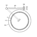
すなわち、めっき層形成部14は、図8および図9に示すように、ケーシング101の内部で基板2を回転保持するための基板回転保持機構(基板収容部)110と、基板2の表面にめっき液や洗浄液などを供給する液供給機構50,90と、基板2から飛散しためっき液や洗浄液などを受けるカップ105と、カップ105で受けためっき液や洗浄液を排出する排出口124,129,134と、排出口に集められた液を排出する液排出機構120,125,130と、基板回転保持機構110、液供給機構50,90,カップ105、および液排出機構120,125,130を制御する制御機構160と、を備えている。
(基板回転保持機構)
このうち基板回転保持機構110は、図8および図9に示すように、ケーシング101内で上下に伸延する中空円筒状の回転軸111と、回転軸111の上端部に取り付けられたターンテーブル112と、ターンテーブル112の上面外周部に設けられ、基板2を支持するウエハチャック113と、回転軸111を回転駆動する回転機構162と、を有している。このうち回転機構162は、制御機構160により制御され、回転機構162によって回転軸111が回転駆動され、これによって、ウエハチャック113により支持されている基板2が回転される。
このうち基板回転保持機構110は、図8および図9に示すように、ケーシング101内で上下に伸延する中空円筒状の回転軸111と、回転軸111の上端部に取り付けられたターンテーブル112と、ターンテーブル112の上面外周部に設けられ、基板2を支持するウエハチャック113と、回転軸111を回転駆動する回転機構162と、を有している。このうち回転機構162は、制御機構160により制御され、回転機構162によって回転軸111が回転駆動され、これによって、ウエハチャック113により支持されている基板2が回転される。
(液供給機構)
次に、基板2の表面にめっき液や洗浄液などを供給する液供給機構50,90について、図8および図9を参照して説明する。液供給機構50,90は、基板2の表面に対してめっき処理を施すめっき液を供給するめっき液供給機構50と、基板2の表面に洗浄処理液を供給する洗浄処理液供給機構90と、を含んでいる。
次に、基板2の表面にめっき液や洗浄液などを供給する液供給機構50,90について、図8および図9を参照して説明する。液供給機構50,90は、基板2の表面に対してめっき処理を施すめっき液を供給するめっき液供給機構50と、基板2の表面に洗浄処理液を供給する洗浄処理液供給機構90と、を含んでいる。
図8および図9に示すように、吐出ノズル52は、ノズルヘッド104に取り付けられている。またノズルヘッド104は、アーム103の先端部に取り付けられており、このアーム103は、上下方向に延伸可能となっており、かつ、回転機構165により回転駆動される支持軸102に固定されている。このような構成により、めっき液を、吐出ノズル52を介して基板2の表面の任意の箇所に所望の高さから吐出することが可能となっている。
(洗浄処理液供給機構90)
洗浄処理液供給機構90は、後述するように基板2の洗浄工程において用いられるものであり、図8に示すように、ノズルヘッド104に取り付けられたノズル92を含んでいる。この場合、ノズル92から、洗浄処理液またはリンス処理液のいずれかが選択的に基板2の表面に吐出される。
洗浄処理液供給機構90は、後述するように基板2の洗浄工程において用いられるものであり、図8に示すように、ノズルヘッド104に取り付けられたノズル92を含んでいる。この場合、ノズル92から、洗浄処理液またはリンス処理液のいずれかが選択的に基板2の表面に吐出される。
(液排出機構)
次に、基板2から飛散しためっき液や洗浄液などを排出する液排出機構120,125,130について、図8を参照して説明する。図8に示すように、ケーシング101内には、昇降機構164により上下方向に駆動され、排出口124,129,134を有するカップ105が配置されている。液排出機構120,125,130は、それぞれ排出口124,129,134に集められる液を排出するものとなっている。
次に、基板2から飛散しためっき液や洗浄液などを排出する液排出機構120,125,130について、図8を参照して説明する。図8に示すように、ケーシング101内には、昇降機構164により上下方向に駆動され、排出口124,129,134を有するカップ105が配置されている。液排出機構120,125,130は、それぞれ排出口124,129,134に集められる液を排出するものとなっている。
図8に示すように、めっき液排出機構120,125は、流路切換器121,126により切り替えられる回収流路122,127および廃棄流路123,128をそれぞれ有している。このうち回収流路122,127は、めっき液を回収して再利用するための流路であり、一方、廃棄流路123,128は、めっき液を廃棄するための流路である。なお図8に示すように、処理液排出機構130には廃棄流路133のみが設けられている。
また図8および図9に示すように、基板収容部110の出口側には、めっき液を排出するめっき液排出機構120の回収流路122が接続され、この回収流路122のうち基板収容部110の出口側近傍に、めっき液を冷却する冷却バッファ120Aが設けられている。
<光学装置の製造方法>
次にこのような構成からなる本実施の形態の作用、すなわち遮光体を含む光学装置の製造方法について図2(a)~(e)により説明する。
次にこのような構成からなる本実施の形態の作用、すなわち遮光体を含む光学装置の製造方法について図2(a)~(e)により説明する。
まず前工程において、半導体ウエハ等からなる基板(シリコン基板)2に対して凹部2aが形成され、凹部2aが形成された基板2が本発明による遮光体を含む光学装置の製造システム10内に搬送される。この場合、基板2上には、Pdイオンが吸着できる金属層21が形成されている(図2(a)参照)。
遮光体を含む光学装置の製造システム10内において、基板2は基板搬送アーム11によって触媒吸着層形成部13へ送られる。そしてこの触媒吸着層形成部13において、基板2の金属層21上に、例えば触媒となるPdイオンが吸着されて触媒吸着層22が形成される(図2(b)参照)。この場合、基板2上に形成された触媒吸着層22は、基板2表面および凹部2a内面に形成されている。
触媒吸着処理としては、例えば、基板2に対して塩化パラジウム水溶液をノズルにより吹付け、触媒となるPdイオンを基板2の表面に吸着させる処理を採用することができる。具体的には、基板2に対して塩化スズ溶液を吹付け、スズイオンを基板2表面に吸着し、次に、基板2に塩化パラジウム水溶液を吹付けてスズイオンをPdイオンと置換してPdイオンを吸着させ、さらに、基板2に水酸化ナトリウムを吹付けて余分なスズイオンを取り除く。
なお、触媒吸着層形成部13の前段に密着層形成部を設け、この密着層形成部内において、凹部2aを有する基板2上にシランカップリング剤等のカップリング剤を吸着させて基板2上に密着層を形成してもよい(SAM処理)。シランカップリング剤を吸着させて形成された密着層は、触媒吸着層22と基板2との密着性を向上させるものである。
次に金属層21上に触媒吸着層22が形成された基板2は、基板搬送アーム11により、触媒吸着層形成部13から焼きしめ部15内へ送られる。そして、この焼きしめ部15の密閉ケーシング内において、基板2は、酸化を抑制するためにN2ガスが充てんされた不活性雰囲気中でホットプレート上で加熱される。このようにして基板2の触媒吸着層22が焼きしめられる(Bake処理)。このように触媒吸着層22を焼きしめることにより、触媒吸着層22内の水分を外方へ放出する。
このように、焼きしめ部15において基板2上に触媒吸着層22を焼きしめた後、基板2は基板搬送アーム11によってめっき層形成部14へ送られる。
次にめっき層形成部14において、基板2の触媒吸着層22上に、CoまたはCo合金を含むめっき層23が形成される(図2(c)参照)。
この場合、めっき層形成部14は、図8および図9に示すようなめっき処理装置からなり、基板2の触媒吸着層22上に無電解めっき処理を施すことによりCoまたはCo合金を含むめっき層23を形成することができる。
めっき層形成部14においてめっき層23を形成する場合、めっき液としては、例えばCo-W-Bを含むめっき液を用いることができ、めっき液の温度は40~75℃(好ましくは65℃)に保たれている。
Co-W-Bを含むめっき液を基板2上に供給することにより、基板2の触媒吸着層22上に無電解めっき処理により、Co-W-Bを含むめっき層23が形成される。
次に触媒吸着層22上にめっき層23が形成された基板2は、基板搬送アーム11によりめっき層形成部14から再び焼きしめ部15に送られ、この焼きしめ部15によりめっき層23が焼きしめられる。
このように基板2上のめっき層23を焼きしめることにより、めっき層23内の水分を外方へ放出することができ、同時にめっき層23内の金属間結合を高めることができる。
次に焼きしめ部15において加熱された基板2は、基板搬送アーム11によりレジストパターン形成部16へ送られる。その後レジストパターン形成部16において、基板2のめっき層23上にレジストパターン27が形成される。この場合、レジストパターン27は基板2の凹部2aに対応する位置に形成される(図2(d)参照)。
次にレジストパターン形成部16においてレジストパターン27が形成された基板2は、基板搬送アーム11によりエッチング処理部17へ送られる。そしてこのエッチング処理部17において、レジストパターン27をマスクとしてめっき層23に対するエッチング処理が施される。このようにしてレジストパターン27により覆われていないめっき層23が除去され、基板2の凹部2aから上方へ延びる遮光体23Aが形成される(図2(e)参照)。次に基板2はレジストパターン除去部17Aまで送られ、このレジストパターン除去部17Aにおいて不要なレジストパターン27が除去される。
次にCo-W-Bを含むめっき層23からなる遮光体23Aの透過率を図4乃至図6により示す。
図4に示すように、Co-W-Bを含む遮光体23Aの赤色光の透過率は、厚さ50~100nmに渡って、NiBからなる遮光体、PVDにより形成されたTaからなる遮光体、PVDにより形成されたWからなる遮光体に比べて低く、良好な遮光特性を示している。
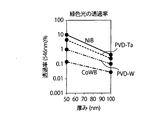
また図5に示すように、Co-W-Bを含む遮光体23Aの緑色光の透過率は、厚さ50~100nmに渡って、NiBからなる遮光体、PVDにより形成されたTaからなる遮光体、PVDにより形成されたWからなる遮光体に比べて低く、良好な遮光特性を示している。
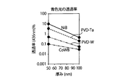
さらに図6に示すように、Co-W-Bを含む遮光体23Aの青色光の透過率は、厚さ50~100nmに渡って、NiBからなる遮光体、PVDにより形成されたTaからなる遮光体、PVDにより形成されたWからなる遮光体に比べて低く、良好な遮光特性を示している。
<本発明の変形例>
次に本発明の変形例について図10(a)~(e)および図11(a)~(d)により説明する。
次に本発明の変形例について図10(a)~(e)および図11(a)~(d)により説明する。
図10(a)~(e)および図11(a)~(d)に示す本発明の変形例は、遮光体を含む光学装置の製造方法が異なるのみであり、他の構成は図1乃至図9に示す実施の形態と略同一である。
図10(a)~(e)および図11(a)~(d)に示す変形例において、図1乃至図9に示す実施の形態と同一部分については同一符号を付して詳細な説明を省略する。
<光学装置の製造方法の第1の変形例>
まず、光学装置の製造方法の第1の変形例について図10(a)~(e)により説明する。
まず、光学装置の製造方法の第1の変形例について図10(a)~(e)により説明する。
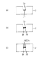
まず前工程において、半導体ウエハ等からなる基板(シリコン基板)2に対して凹部2aが形成され、凹部2aが形成された基板2が本発明による遮光体を含む光学装置の製造システム10内に搬送される。この場合、基板2上には、Pdイオンが吸着できる金属層21が形成されている(図10(a)参照)。
次に遮光体を含む光学装置の製造システム10内において、基板2は基板搬送アーム11によって触媒吸着層形成部13へ送られる。そしてこの触媒吸着層形成部13において、基板2の金属層21上に、例えば触媒となるPdイオンが吸着されて触媒吸着層22が形成される(図10(b)参照)。この場合、基板2上に形成された触媒吸着層22は、基板2表面および凹部2a内面に形成されている。
触媒吸着処理としては、例えば、基板2に対して塩化パラジウム水溶液をノズルにより吹付け、触媒となるPdイオンを基板2の表面に吸着させる処理を採用することができる。具体的には、基板2に対して塩化スズ溶液を吹付け、スズイオンを基板2表面に吸着し、次に、基板2に塩化パラジウム水溶液を吹付けてスズイオンをPdイオンと置換してPdイオンを吸着させ、さらに、基板2に水酸化ナトリウムを吹付けて余分なスズイオンを取り除く。
なお、触媒吸着層形成部13の前段に密着層形成部を設け、この密着層形成部内において、凹部2aを有する基板2上にシランカップリング剤等のカップリング剤を吸着させて基板2上に密着層を形成してもよい(SAM処理)。シランカップリング剤を吸着させて形成された密着層は、触媒吸着層22と基板2との密着性を向上させるものである。
次に金属層21上に触媒吸着層22が形成された基板2は、基板搬送アーム11により、触媒吸着層形成部13から焼きしめ部15内へ送られる。そして、この焼きしめ部15の密閉ケーシング内において、基板2は、酸化を抑制するためにN2ガスが充てんされた不活性雰囲気中でホットプレート上で加熱される。このようにして基板2の触媒吸着層22が焼きしめられる(Bake処理)。このように触媒吸着層22を焼きしめることにより、触媒吸着層22内の水分を外方へ放出する。
このように、焼きしめ部15において基板2上の触媒吸着層22を焼きしめた後、基板2は基板搬送アーム11によってレジストパターン形成部16へ送られる。そしてこのレジストパターン形成部16において、触媒吸着層22上に開口27aを有するレジストパターン27が形成される(図10(c)参照)。ここでレジストパターン27の開口27aは基板2の凹部2aを囲んで形成されている。
次に基板2は基板搬送アーム11によってめっき層形成部14へ送られ、このめっき層形成部14において、レジストパターン27の開口27a内にCoまたはCo合金を含むめっき層23が形成される(図10(d)参照)。
この場合、めっき層形成部14は、図8および図9に示すようなめっき処理装置からなり、基板2の触媒吸着層22上に無電解めっき処理を施すことによりCoまたはCo合金を含むめっき層23を形成することができる。
めっき層形成部14においてめっき層23を形成する場合、めっき液としては、例えばCo-W-Bを含むめっき液を用いることができ、めっき液の温度は40~75℃(好ましくは65℃)に保たれている。
Co-W-Bを含むめっき液を基板2上に供給することにより、レジストパターン27の開口27a内に形成された触媒吸着層22上に無電解めっき処理により、Co-W-Bを含むめっき層23が形成される。
次に触媒吸着層22上にめっき層23が形成された基板2は、基板搬送アーム11によりめっき層形成部14から再び焼きしめ部15に送られ、この焼きしめ部15によりめっき層23が焼きしめられる。
このように基板2上のめっき層23を焼きしめることにより、めっき層23内の水分を外方へ放出することができ、同時にめっき層23内の金属間結合を高めることができる。
次に基板2のレジストパターン27の開口27a内にめっき層23が形成された基板2は、基板搬送アーム11によりレジストパターン除去部17Aまで送られ、このレジストパターン除去部17Aにおいてレジストパターン27が除去される。このようにして基板2上に凹部2aから上方へ延びるとともにめっき層23により形成された遮光体23Aを得ることができる(図10(e)参照)。
<光学装置の製造方法の第2の変形例>
次に光学装置の製造方法の第2の変形例について図11(a)~(c)により説明する。
次に光学装置の製造方法の第2の変形例について図11(a)~(c)により説明する。
まず前工程において、半導体ウエハ等からなる基板(シリコン基板)2に対して凹部2aが形成され、凹部2aが形成された基板2が本発明による遮光体を含む光学装置の製造システム10内に搬送される。この場合、基板2の凹部2aの底面にはPdイオンが吸着できる金属層21が形成されている。
次に遮光体を含む光学装置の製造システム10内において、基板2は基板搬送アーム11によって触媒吸着層形成部13へ送られる。そしてこの触媒吸着層形成部13において、基板2の凹部2a底面に設けられた金属層21上に、例えば触媒となるPdイオンが吸着されて触媒吸着層22が形成される(図11(b)参照)。
触媒吸着処理としては、例えば、基板2に対して塩化パラジウム水溶液をノズルにより吹付け、触媒となるPdイオンを基板2の凹部2a底面に吸着させる処理を採用することができる。具体的には、基板2に対して塩化スズ溶液を吹付け、スズイオンを基板2の凹部2a底面に吸着し、次に、基板2に塩化パラジウム水溶液を吹付けてスズイオンをPdイオンと置換してPdイオンを吸着させ、さらに、基板2に水酸化ナトリウムを吹付けて余分なスズイオンを取り除く。
なお、触媒吸着層形成部13の前段に密着層形成部を設け、この密着層形成部内において、凹部2aの底面にシランカップリング剤等のカップリング剤を吸着させて基板2の凹部2a底面に密着層を形成してもよい(SAM処理)。シランカップリング剤を吸着させて形成された密着層は、触媒吸着層22と基板2の凹部2a底面との密着性を向上させるものである。
次に凹部2a底面の金属層21上に触媒吸着層22が形成された基板2は、基板搬送アーム11により、触媒吸着層形成部13から焼きしめ部15内へ送られる。そして、この焼きしめ部15の密閉ケーシング内において、基板2は、酸化を抑制するためにN2ガスが充てんされた不活性雰囲気中でホットプレート上で加熱される。このようにして基板2の触媒吸着層22が焼きしめられる(Bake処理)。このように触媒吸着層22を焼きしめることにより、触媒吸着層22内の水分を外方へ放出する。
このように、焼きしめ部15において基板2の凹部2a底面上の触媒吸着層22を焼きしめた後、基板2は基板搬送アーム11によってめっき層形成部14へ送られる。
次にめっき層形成部14において、基板2の触媒吸着層22上に、CoまたはCo合金を含むめっき層23が形成される(図11(c)参照)。
この場合、めっき層形成部14は、図5および図6に示すようなめっき処理装置からなり、基板2の凹部2a底面に形成された触媒吸着層22上に無電解めっき処理を施すことによりCoまたはCo合金を含むめっき層23を形成することができる。めっき層23は基板2の凹部2a底面に形成された触媒吸着層22から上方へ成長し、凹部2a全域がめっき層23により埋め込まれる。
めっき層形成部14においてめっき層23を形成する場合、めっき液としては、例えばCo-W-Bを含むめっき液を用いることができ、めっき液の温度は40~75℃(好ましくは65℃)に保たれている。
Co-W-Bを含むめっき液を基板2上に供給することにより、基板2の凹部2a底面に形成された触媒吸着層22上に無電解めっき処理により、Co-W-Bを含むめっき層23が形成される。
次に触媒吸着層22上にめっき層23が形成された基板2は、基板搬送アーム11によりめっき層形成部14から再び焼きしめ部15に送られ、この焼きしめ部15によりめっき層23が焼きしめられる。
このように基板2上のめっき層23を焼きしめることにより、めっき層23内の水分を外方へ放出することができ、同時にめっき層23内の金属間結合を高めることができる。
このようにして基板2の凹部2a内にめっき層23を埋め込むことができ、このめっき層23によって遮光体23Aを得ることができる。なお凹部2a内に埋め込まれためっき層23を更に成長させることにより、基板2の凹部2aから上方へ突出する遮光体23Aを得ることができる。
なお、上記各実施の形態および変形例において、遮光体を含む光学装置として固体撮像素子の例を示したが、これに限らず遮光体を含む光学装置として例えばLEDと、カラーフィルタと、遮光体とを含むタッチパネル付の表示装置を用いてもよい。
また、上記実施例においては、めっき層形成部14と焼きしめ部15とを別々の装置で構成した例を示したが、これに限ることはなく、図8で示すめっき層形成部14において、基板2の上方にランプ照射部200(UV光など)、または基板2を覆うホットプレート(図示せず)などの加熱源を設け、めっき層形成部14内でめっき層の焼きしめを行ってもよい。
2 基板
2a 凹部
10 光学装置の製造システム
11 基板搬送アーム
13 触媒吸着層形成部
14 めっき層形成部
15 焼きしめ部
16 レジストパターン形成部
17 エッチング処理部
17A レジストパターン除去部
18 カセットステーション
19 制御部
19A 記憶媒体
21 金属層
22 触媒吸着層
23 めっき層
23A 遮光体
27 レジストパターン
30 固体撮像素子
35 カラーフィルタ層
36 フォトダイオード
2a 凹部
10 光学装置の製造システム
11 基板搬送アーム
13 触媒吸着層形成部
14 めっき層形成部
15 焼きしめ部
16 レジストパターン形成部
17 エッチング処理部
17A レジストパターン除去部
18 カセットステーション
19 制御部
19A 記憶媒体
21 金属層
22 触媒吸着層
23 めっき層
23A 遮光体
27 レジストパターン
30 固体撮像素子
35 カラーフィルタ層
36 フォトダイオード
Claims (2)
- 遮光体を含む光学装置の製造方法において、
基板を準備する工程と、
前記基板上にCoまたはCo合金を含むめっき液を供給して無電解めっき処理を施すことにより、前記遮光体となるCoまたはCo合金のめっき層を形成する工程と、
を備えたことを特徴とする遮光体を含む光学装置の製造方法。 - 遮光体を含む光学装置の製造システムに光学装置の製造方法を実行させるためのコンピュータプログラムを格納した記憶媒体において、
光学装置の製造方法は、
基板を準備する工程と、
前記基板上にCoまたはCo合金を含むめっき液を供給して無電解めっき処理を施すことにより、前記遮光体となるCoまたはCo合金のめっき層を形成する工程と、
を備えたことを特徴とする記憶媒体。
Priority Applications (1)
| Application Number | Priority Date | Filing Date | Title |
|---|---|---|---|
| KR1020177023083A KR102486977B1 (ko) | 2015-02-19 | 2016-01-28 | 차광체를 포함하는 광학 장치의 제조 방법 및 기억 매체 |
Applications Claiming Priority (2)
| Application Number | Priority Date | Filing Date | Title |
|---|---|---|---|
| JP2015030918A JP6339032B2 (ja) | 2015-02-19 | 2015-02-19 | 遮光体を含む光学装置の製造方法、および記憶媒体 |
| JP2015-030918 | 2015-02-19 |
Publications (1)
| Publication Number | Publication Date |
|---|---|
| WO2016132850A1 true WO2016132850A1 (ja) | 2016-08-25 |
Family
ID=56692140
Family Applications (1)
| Application Number | Title | Priority Date | Filing Date |
|---|---|---|---|
| PCT/JP2016/052550 Ceased WO2016132850A1 (ja) | 2015-02-19 | 2016-01-28 | 遮光体を含む光学装置の製造方法、および記憶媒体 |
Country Status (4)
| Country | Link |
|---|---|
| JP (1) | JP6339032B2 (ja) |
| KR (1) | KR102486977B1 (ja) |
| TW (1) | TWI626333B (ja) |
| WO (1) | WO2016132850A1 (ja) |
Families Citing this family (1)
| Publication number | Priority date | Publication date | Assignee | Title |
|---|---|---|---|---|
| JP7637162B2 (ja) * | 2021-02-02 | 2025-02-27 | 株式会社ジャパンディスプレイ | 検出装置及び検出装置の製造方法 |
Citations (1)
| Publication number | Priority date | Publication date | Assignee | Title |
|---|---|---|---|---|
| JPH02146771A (ja) * | 1988-11-28 | 1990-06-05 | Dainippon Printing Co Ltd | カラー固体撮像装置の製造方法 |
Family Cites Families (10)
| Publication number | Priority date | Publication date | Assignee | Title |
|---|---|---|---|---|
| US6150683A (en) * | 1997-06-27 | 2000-11-21 | Foveon, Inc. | CMOS-based color pixel with reduced noise in the blue signal |
| JPH11318090A (ja) * | 1998-05-07 | 1999-11-16 | Canon Inc | 振動型駆動装置、その製造方法およびそれを備えた機器 |
| JP2005166757A (ja) * | 2003-11-28 | 2005-06-23 | Advanced Lcd Technologies Development Center Co Ltd | 配線構造体、配線構造体の形成方法、薄膜トランジスタ、薄膜トランジスタの形成方法、及び表示装置 |
| JP4507769B2 (ja) * | 2004-08-31 | 2010-07-21 | ソニー株式会社 | 固体撮像素子、カメラモジュール及び電子機器モジュール |
| JP4396684B2 (ja) * | 2006-10-04 | 2010-01-13 | ソニー株式会社 | 固体撮像装置の製造方法 |
| JP4751865B2 (ja) | 2007-09-10 | 2011-08-17 | 富士フイルム株式会社 | 裏面照射型固体撮像素子及びその製造方法 |
| JP5434121B2 (ja) | 2009-02-17 | 2014-03-05 | 株式会社ニコン | 裏面照射型撮像素子および撮像装置 |
| KR101786069B1 (ko) * | 2009-02-17 | 2017-10-16 | 가부시키가이샤 니콘 | 이면 조사형 촬상 소자, 그 제조 방법 및 촬상 장치 |
| JP5714428B2 (ja) * | 2011-06-24 | 2015-05-07 | 東京エレクトロン株式会社 | めっき処理装置、めっき処理方法および記憶媒体 |
| JP6130221B2 (ja) * | 2013-05-24 | 2017-05-17 | ソニー株式会社 | 固体撮像装置、および電子機器 |
-
2015
- 2015-02-19 JP JP2015030918A patent/JP6339032B2/ja active Active
-
2016
- 2016-01-28 WO PCT/JP2016/052550 patent/WO2016132850A1/ja not_active Ceased
- 2016-01-28 KR KR1020177023083A patent/KR102486977B1/ko active Active
- 2016-02-17 TW TW105104613A patent/TWI626333B/zh active
Patent Citations (1)
| Publication number | Priority date | Publication date | Assignee | Title |
|---|---|---|---|---|
| JPH02146771A (ja) * | 1988-11-28 | 1990-06-05 | Dainippon Printing Co Ltd | カラー固体撮像装置の製造方法 |
Also Published As
| Publication number | Publication date |
|---|---|
| TWI626333B (zh) | 2018-06-11 |
| KR20170118088A (ko) | 2017-10-24 |
| JP2016152403A (ja) | 2016-08-22 |
| JP6339032B2 (ja) | 2018-06-06 |
| KR102486977B1 (ko) | 2023-01-10 |
| TW201702428A (zh) | 2017-01-16 |
Similar Documents
| Publication | Publication Date | Title |
|---|---|---|
| US9024405B2 (en) | Solid-state image sensor | |
| TWI479650B (zh) | 改良式背側發光影像感測器架構及其製造方法 | |
| CN102446933B (zh) | 固体摄像装置及其制造方法和电子设备 | |
| CN108550599B (zh) | 具有掩埋光屏蔽件和垂直栅极的图像传感器 | |
| JP4639212B2 (ja) | 裏面照射型撮像素子の製造方法 | |
| US8008192B2 (en) | Conductive interconnect structures and formation methods using supercritical fluids | |
| CN101740596B (zh) | 固态成像器,其制造方法和照相机 | |
| CN111512443B (zh) | 摄像元件和摄像装置 | |
| JP6673839B2 (ja) | 固体撮像素子および製造方法、並びに電子機器 | |
| US20060290001A1 (en) | Interconnect vias and associated methods of formation | |
| CN101292352A (zh) | 微电子成像单元和以晶片级制造微电子成像单元的方法 | |
| JP2013243364A (ja) | 半導体装置およびその製造方法 | |
| CN104347657A (zh) | 固态成像装置、其制造方法以及电子设备 | |
| CN101308821A (zh) | 制造图像传感器的方法 | |
| CN1992212A (zh) | 制造cmos图像传感器的方法 | |
| CN105702695B (zh) | 一种背照式传感器的制备方法 | |
| JP6339032B2 (ja) | 遮光体を含む光学装置の製造方法、および記憶媒体 | |
| JP4621048B2 (ja) | 固体撮像素子 | |
| JP2008306192A (ja) | 半導体基板およびその製造方法、半導体素子の製造方法およびイメージセンサの製造方法 | |
| US7169633B2 (en) | Solid-state image sensor for improving sensing quality and manufacturing method thereof | |
| CN111799282A (zh) | 具有屏蔽互连器的图像传感器 | |
| JP2010093160A (ja) | 固体撮像装置とその製造方法並びに電子機器 | |
| JP2010283082A (ja) | 固体撮像装置、電子機器および固体撮像装置の製造方法 | |
| TWI806991B (zh) | 攝像元件及攝像元件之製造方法 | |
| JP5327146B2 (ja) | 固体撮像装置とその製造方法、及びカメラ |
Legal Events
| Date | Code | Title | Description |
|---|---|---|---|
| 121 | Ep: the epo has been informed by wipo that ep was designated in this application |
Ref document number: 16752239 Country of ref document: EP Kind code of ref document: A1 |
|
| ENP | Entry into the national phase |
Ref document number: 20177023083 Country of ref document: KR Kind code of ref document: A |
|
| NENP | Non-entry into the national phase |
Ref country code: DE |
|
| 122 | Ep: pct application non-entry in european phase |
Ref document number: 16752239 Country of ref document: EP Kind code of ref document: A1 |