WO2016129106A1 - バッテリ充電装置、およびバッテリ充電装置の制御方法 - Google Patents
バッテリ充電装置、およびバッテリ充電装置の制御方法 Download PDFInfo
- Publication number
- WO2016129106A1 WO2016129106A1 PCT/JP2015/053982 JP2015053982W WO2016129106A1 WO 2016129106 A1 WO2016129106 A1 WO 2016129106A1 JP 2015053982 W JP2015053982 W JP 2015053982W WO 2016129106 A1 WO2016129106 A1 WO 2016129106A1
- Authority
- WO
- WIPO (PCT)
- Prior art keywords
- battery
- terminal
- bipolar transistor
- control circuit
- signal
- Prior art date
- Legal status (The legal status is an assumption and is not a legal conclusion. Google has not performed a legal analysis and makes no representation as to the accuracy of the status listed.)
- Ceased
Links
Images


Classifications
-
- H—ELECTRICITY
- H02—GENERATION; CONVERSION OR DISTRIBUTION OF ELECTRIC POWER
- H02J—ELECTRIC POWER NETWORKS; CIRCUIT ARRANGEMENTS OR SYSTEMS FOR SUPPLYING OR DISTRIBUTING ELECTRIC POWER; SYSTEMS FOR STORING ELECTRIC ENERGY
- H02J7/00—Circuit arrangements for charging or discharging batteries or for supplying loads from batteries
-
- H—ELECTRICITY
- H02—GENERATION; CONVERSION OR DISTRIBUTION OF ELECTRIC POWER
- H02J—ELECTRIC POWER NETWORKS; CIRCUIT ARRANGEMENTS OR SYSTEMS FOR SUPPLYING OR DISTRIBUTING ELECTRIC POWER; SYSTEMS FOR STORING ELECTRIC ENERGY
- H02J7/00—Circuit arrangements for charging or discharging batteries or for supplying loads from batteries
- H02J7/14—Circuit arrangements for charging or discharging batteries or for supplying loads from batteries for charging batteries from dynamo-electric generators driven at varying speed, e.g. on vehicle
Definitions
- the present invention relates to a battery charger and a method for controlling the battery charger.
- a switch element (thyristor) SW1 having a first node connected to the first generator terminal TD1 and a second node connected to the first battery terminal TB1.
- a control circuit CON that controls the operation of the switch element SW1 according to the input voltage VIN between the first generator terminal TD1 and the second generator terminal TD2, and the first battery terminal TB1 and the second battery terminal TB1.
- the control circuit CON turns on the switch element SW1 according to the charge permission signal, and turns off the switch element SW1 according to the charge stop signal.
- control circuit CON turns off the switch element SW1 when the input voltage VIN becomes less than the specified value.
- the battery voltage detection circuit BVD outputs the charge permission signal. To do.
- the control circuit CON sets the switch element SW1 when the input voltage VIN is less than the specified value. Turn off (FIG. 5). Thereby, the current I1a flowing through the coil LG of the single-phase AC generator G is blocked by the switch element SW1 (FIG. 5).
- the control circuit CON supplies the current I1b to the gate of the switch element (thyristor) SW1, and turns on the switch element SW1 (FIG. 6).
- the control circuit CON supplies the current I1b to the gate of the switch element (thyristor) SW1, and turns on the switch element SW1 (FIG. 6).
- large currents I1a and I3a flow from the battery charging device 100A.
- Such a large current can cause heat generation and destruction of elements, circuits, batteries, and the like.
- the conventional battery charger has a problem that a large current flows when the single-phase AC generator rotates and starts generating power when the battery is reversely connected.
- An object of the present invention is to provide a battery charging device and a battery charging device control method capable of suppressing the flow of the battery.
- a battery charger includes: A battery charging device that controls charging of a battery by a single-phase AC generator, A first generator terminal to which one end of the coil of the single-phase AC generator is connected; A second generator terminal to which the other end of the coil is connected and grounded; A first battery terminal to which the positive electrode of the battery is connected when the battery is normally connected and a second battery which is connected to the second generator terminal and to which the negative electrode of the battery is connected when the battery is normally connected A terminal, A switch element having a first node connected to the first generator terminal and a second node connected to the first battery terminal; A control circuit for controlling the operation of the switch element according to an input voltage between the first generator terminal and the second generator terminal; An output voltage between the first battery terminal and the second battery terminal is detected, and when the output voltage is a positive target value or more, a charge stop signal is output to the control circuit, A battery voltage detection circuit that outputs a charge permission signal to the control circuit when the output voltage is less than the target value; If,
- the switch element is a thyristor in which the first node is an anode and the second node is a cathode.
- the control circuit includes: A first diode having an anode connected to the first generator terminal; A first PNP-type bipolar transistor having an emitter connected to the cathode of the first diode; A second diode having an anode connected to the collector of the first PNP-type bipolar transistor and a cathode connected to the gate of the thyristor; The collector is connected to the base of the first PNP-type bipolar transistor, the emitter is connected to the second generator terminal, and the base is connected to a signal node to which the charge stop signal or the charge permission signal is input.
- a first NPN bipolar transistor A first resistance element connected between a base and an emitter of the first NPN-type bipolar transistor,
- the control circuit includes: When the input voltage exceeds the specified value, The first NPN bipolar transistor is turned on by turning on the first NPN bipolar transistor in response to the charge permission signal, or the first NPN bipolar transistor in response to the charge stop signal. Turns off the first PNP-type bipolar transistor, When the input voltage becomes less than the specified value, When the first NPN bipolar transistor is turned off, the first PNP bipolar transistor is turned off. When the reverse connection detection signal is input when the input voltage is equal to or higher than the specified value and the charge permission signal is input, the first NPN bipolar transistor is forcibly turned off. The first PNP-type bipolar transistor is turned off.
- the control circuit includes: It further comprises a second resistance element connected between the cathode of the first diode and the base of the first NPN bipolar transistor.
- the control circuit includes: A third resistance element connected between the base of the first PNP bipolar transistor and the collector of the first NPN bipolar transistor is further provided.
- the control circuit includes: A fourth resistance element connected between the collector of the first PNP-type bipolar transistor and the anode of the second diode is further provided.
- the battery voltage detection circuit includes: A third diode having an anode connected to the first battery terminal; A Zener diode having a cathode connected to the cathode of the third diode; A collector is connected to the signal node, an emitter is connected to the second battery terminal, a base is connected to the anode of the Zener diode, and the charge stop signal or the charge permission signal is output from the collector. And an NPN-type bipolar transistor.
- the battery voltage detection circuit includes: When the output voltage is equal to or higher than the target value, by turning on the second NPN bipolar transistor, the charge stop signal is output to the signal node, On the other hand, when the output voltage is less than the target value, the charge permission signal is output to the signal node by turning on the second NPN bipolar transistor.
- the battery voltage detection circuit includes: A fifth resistance element connected between the anode of the Zener diode and the base of the second NPN bipolar transistor is further provided.
- the reverse connection detection circuit includes: A fourth diode having a cathode connected to the first battery terminal; A sixth resistance element connected between the anode of the fourth diode and the signal node; A fifth diode having a cathode connected to the signal node and an anode connected to the second battery terminal;
- the reverse connection detection circuit includes: When reverse connection of the battery is detected based on the output voltage, the reverse connection detection signal is output to the signal node.
- the reverse connection detection circuit includes: If the output voltage is negative polarity, output the reverse connection detection signal, On the other hand, when the output voltage has a positive polarity, the reverse connection detection signal is not output.
- the single-phase AC generator is an alternator that is directly connected to the engine of a motorcycle, and the single-phase AC generator rotates to generate electric power by the operation of a kick pedal by a user.
- a battery charging method includes: A battery charging device for controlling charging of a battery by a single-phase AC generator, wherein a first generator terminal to which one end of a coil of the single-phase AC generator is connected, and the other end of the coil are connected; The second generator terminal to be grounded, the first battery terminal to which the positive electrode of the battery is connected when the battery is normally connected, and the second generator terminal are connected, and the battery is normally connected to the second generator terminal.
- a charge stop signal is output to the control circuit.
- a charge permission signal is output to the control circuit.
- a battery voltage detection circuit for outputting to the circuit, and based on the output voltage, the positive electrode of the battery is connected to the second battery terminal and the negative electrode of the battery is connected to the first battery terminal.
- a reverse connection detection circuit that outputs a reverse connection detection signal to the control circuit when a reverse connection is detected; When the input voltage becomes a specified value or more, if the charge permission signal is input, the switch element is turned on, or if the charge stop signal is input, the switch element is turned off, When the input voltage becomes less than the specified value, the switch element is turned off, In the case where the input voltage is equal to or higher than the specified value and the charge permission signal is input, the switch element is forcibly turned off when the reverse connection detection signal is input.
- a battery charging device includes a first generator terminal to which one end of a coil of a single-phase AC generator is connected, and a second generator terminal to which the other end of the coil is connected and grounded.
- a switching element thyristor having a first node connected to the first generator terminal and a second node connected to the first battery terminal, and between the first generator terminal and the second generator terminal
- the control circuit turns on the switch element if the charge permission signal is inputted when the input voltage becomes the specified value or more, and turns off the switch element if the charge stop signal is inputted.
- control circuit turns off the switch element when the input voltage becomes less than the specified value.
- control circuit forcibly turns off the switch element when the reverse connection detection signal is input when the input voltage is equal to or higher than the specified value and the charge permission signal is input (FIG. 2).
- the battery charging device of the present embodiment when the single-phase AC generator rotates and starts power generation when the battery is reversely connected (when the input voltage is equal to or higher than the specified value), the charging current is allowed to flow.
- the switch element is forcibly turned off regardless of other conditions (battery charging voltage).
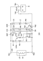
- FIG. 1 is a circuit diagram illustrating an example of a circuit configuration of the battery charging device 100 according to the first embodiment.
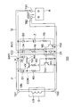
- FIG. 2 is a diagram for explaining an example of the operation of the battery charging device 100 when the single-phase AC generator G is stopped in a state where the battery charging device 100 shown in FIG.
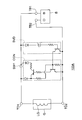
- FIG. 3 illustrates an example of the operation of the battery charging apparatus 100 when the single-phase AC generator G is driven (power generation) in the state where the battery charging apparatus 100 illustrated in FIG.
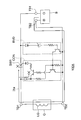
- FIG. 4 is a circuit diagram showing an example of a circuit configuration of a conventional battery charging device 100A.
- FIG. 5 is a diagram for explaining an example of the operation of the battery charging device 100A when the single-phase AC generator G is stopped in the state where the battery charging device 100A shown in FIG.
- FIG. 6 illustrates an example of the operation of the battery charging device 100A when the single-phase AC generator G is driven (power generation) in a state where the battery charging device 100A shown in FIG.
- FIG. 5 is a diagram for explaining
- the battery charger 100 controls the charging of the battery B by the single-phase AC generator G (FIG. 1).
- the example of FIG. 1 shows a state where the battery B is normally connected to the battery charging device 100.
- the battery charger 100 includes a first generator terminal TD1 to which one end of a coil LG of a single-phase AC generator G is connected, and a second generator terminal TD2 to which the other end of the coil LG is connected and grounded. (FIG. 1).
- the single-phase AC generator G is, for example, an alternator that is directly connected to a motorcycle engine. In this case, the single-phase AC generator G rotates to generate power with the driving of the engine. However, even when the engine is stopped, for example, the single-phase AC generator G is rotated to generate power by the operation of the kick pedal by the user.
- the battery charger 100 is connected to the first battery terminal TB1 to which the positive electrode of the battery B is connected when the battery B is normally connected and the second generator terminal TD2, and the negative electrode of the battery B when the battery is normally connected. Is connected to the second battery terminal TB2 (FIG. 1).
- a load circuit (not shown) is connected between the first battery terminal TB1 and the second battery terminal TB2.
- the battery charging apparatus 100 includes a switch element SW1 having a first node connected to the first generator terminal TD1 and a second node connected to the first battery terminal TB1.
- the switch element SW1 is a thyristor in which the first node is an anode and the second node is a cathode (hereinafter also referred to as a thyristor SW1 if necessary).
- the battery charging device 100 includes a battery voltage detection circuit BVD that detects an output voltage VOUT between the first battery terminal TB1 and the second battery terminal TB2 (FIG. 1).
- the battery voltage detection circuit BVD includes, for example, a third diode D3 whose anode is connected to the first battery terminal TB1, and a Zener diode Z whose cathode is connected to the cathode of the third diode D3 ( FIG. 1).
- the battery voltage detection circuit BVD has a collector connected to the signal node NS, an emitter connected to the second battery terminal TB2, a base connected to the anode of the Zener diode Z, and a charge stop signal or charge permission signal from the collector. And a fifth resistance element R5 connected between the anode of the Zener diode Z and the base of the second NPN bipolar transistor Yb2 (FIG. 1). .
- the battery voltage detection circuit BVD when the output voltage VOUT is equal to or higher than the positive target value, the battery voltage detection circuit BVD outputs a charge stop signal for stopping the charging of the battery B to the control circuit CON.
- the battery voltage detection circuit BVD turns on the second NPN bipolar transistor Yb2 to output a charge stop signal to the signal node NS.
- the potential of the signal node NS (base of the first NPN bipolar transistor Yb1) becomes equal to the potential of the emitter of the first NPN bipolar transistor Yb1, and the first NPN bipolar transistor Yb1 is turned off. It becomes.
- the battery voltage detection circuit BVD outputs a charge permission signal for permitting charging of the battery B to the control circuit CON.
- the battery voltage detection circuit BVD when the output voltage VOUT is less than the target value, the battery voltage detection circuit BVD outputs the charge permission signal to the signal node NS by turning off the second NPN bipolar transistor Yb2.
- the first NPN bipolar transistor Yb1 can be turned on in accordance with the current flowing through the first resistor R1.
- the battery charging apparatus 100 is configured to reversely connect the battery B in which the positive electrode of the battery B is connected to the second battery terminal TB2 and the negative electrode of the battery B is connected to the first battery terminal TB1 based on the output voltage VOUT. Is detected, a reverse connection detection circuit ICD that outputs a reverse connection detection signal to the control circuit CON is provided.
- the reverse connection detection circuit ICD includes, for example, a fourth diode D4 whose cathode is connected to the first battery terminal TB1, and a sixth diode connected between the anode of the fourth diode D4 and the signal node NS.
- Resistance element R6, and a fifth diode D5 having a cathode connected to the signal node NS and an anode connected to the second battery terminal TB2 (FIG. 1).
- the reverse connection detection circuit ICD When the reverse connection of the battery B is detected based on the output voltage VOUT, the reverse connection detection circuit ICD outputs the reverse connection detection signal to the signal node NS.
- output voltage VOUT has a negative polarity. That is, the reverse connection detection circuit ICD outputs the reverse connection detection signal when the output voltage VOUT has a negative polarity.
- the reverse connection detection circuit ICD is directed from the fifth diode D5 to the fourth diode D4 via the signal node NS and the sixth resistor R6. Current flows. As a result, the potential of the signal node NS (the cathode of the fifth diode D5) (the reverse connection detection signal) is lower than the potential of the anode of the fifth diode D5.
- a reverse voltage is applied between the base (signal node NS) and the emitter (the anode of the fifth diode D5) of the first NPN-type bipolar transistor Yb1 of the control circuit CON described later.
- the first NPN bipolar transistor Yb1 is turned off.
- the reverse connection detection circuit ICD does not detect the reverse connection of the battery B based on the output voltage VOUT, the reverse connection detection signal is not output to the signal node NS.
- output voltage VOUT has a positive polarity. That is, the reverse connection detection circuit ICD does not output the reverse connection detection signal when the output voltage VOUT has a positive polarity.
- the battery charging device 100 includes a control circuit CON that controls the operation of the switch element SW1 according to the input voltage VIN between the first generator terminal TD1 and the second generator terminal TD2.
- the control circuit CON includes, for example, a first diode D1 whose anode is connected to the first generator terminal TD1, and a first PNP-type bipolar transistor Ya1 whose emitter is connected to the cathode of the first diode D1. And a second diode D2 having an anode connected to the collector of the first PNP-type bipolar transistor Ya1 and a cathode connected to the gate of the thyristor SW1 (FIG. 1).
- control circuit CON has a collector connected to the base of the first PNP-type bipolar transistor Ya1, an emitter connected to the second generator terminal TD2, and a base to which a charge stop signal or charge permission signal is input.
- a first NPN-type bipolar transistor Yb1 connected to the node NS is provided (FIG. 1).
- control circuit CON includes a first resistance element R1 connected between the base and emitter of the first NPN type bipolar transistor Yb1, a cathode of the first diode D1, and the first NPN type bipolar transistor Yb1. And a second resistance element R2 connected between the base of the first and second bases (FIG. 1).
- control circuit CON includes a third resistance element R3 connected between the base of the first PNP bipolar transistor Ya1 and the collector of the first NPN bipolar transistor Yb1, and a first PNP bipolar transistor.
- a fourth resistance element R4 connected between the collector of Ya1 and the anode of the second diode D2 (FIG. 1).
- the control circuit CON turns on the switch element (thyristor) SW1 if a charge permission signal permitting charging is input via the signal node Ns when the input voltage VIN becomes equal to or higher than the specified value.
- control circuit CON turns on the first NPN bipolar transistor Yb1 in response to the charge permission signal when the input voltage VIN becomes equal to or higher than a specified value (here, for example, a positive voltage). Then, the first PNP bipolar transistor Ya1 is turned on.
- a specified value here, for example, a positive voltage
- the positive voltage generated by the single-phase AC generator G is supplied to the battery B, and the battery B is charged.
- the control circuit CON turns off the switch element (thyristor) SW1 when a charge stop signal for stopping charging is input via the signal node NS when the input voltage VIN becomes equal to or higher than the specified value.
- the first NPN bipolar transistor Yb1 when the input voltage VIN becomes equal to or higher than the specified value, the first NPN bipolar transistor Yb1 is turned off in response to the charge stop signal, so that the first PNP bipolar transistor Ya1 is turned on. Turn off.
- the control circuit CON turns off the switch element SW1 when the input voltage VIN is less than the specified value (here, for example, a negative voltage).
- control circuit CON turns off the first PNP bipolar transistor Ya1 by turning off the first NPN bipolar transistor Yb1 when the input voltage VIN becomes less than the specified value.
- control circuit CON forcibly turns on the switch element SW1 when the reverse connection of the battery B is detected even when the switch B is turned on and the battery B is charged. To come off.
- the control circuit CON switches the switch element SW1. Forcibly turn off.
- the control circuit CON receives the first NPN bipolar transistor Yb1. Since a reverse voltage is applied between the base and the emitter, the first NPN bipolar transistor Yb1 is forcibly turned off. As a result, the control circuit CON is configured so that the first PNP-type bipolar transistor Ya1 is turned off.
- the battery charging device 100 is in a reverse connection state of the battery B in which the positive electrode of the battery B is connected to the second battery terminal TB2 and the negative electrode of the battery B is connected to the first battery terminal TB1. To do.
- the reverse connection detection circuit ICD has a current flowing from the fifth diode D5 to the fourth diode D4 via the signal node NS and the sixth resistor R6. I2 flows (FIG. 2).
- the reverse connection detection circuit ICD detects the reverse connection of the battery B and outputs the reverse connection detection signal to the signal node NS. To do.
- the battery voltage detection circuit BVD outputs the charge permission signal.
- the control circuit CON sets the switch element SW1 when the input voltage VIN is less than the specified value. Turn off (FIG. 2). Thereby, the current I1 flowing through the coil LG of the single-phase AC generator G is interrupted by the switch element SW1 (FIG. 2).
- a current I3 flows through the first diode D1, the second resistor R2, the signal node NS, the sixth resistor R6, and the fourth diode D4 of the control circuit CON (FIG. 3).
- the reverse connection detection circuit ICD is directed from the fifth diode D5 to the fourth diode D4 via the signal node NS and the sixth resistor R6.
- Current I2 flows (FIG. 3).
- the reverse connection detection circuit ICD detects the reverse connection of the battery B and outputs the reverse connection detection signal to the signal node NS. To do.
- the control circuit CON does not supply a predetermined current to the gate of the thyristor SW1, so that the thyristor SW1 is turned off when the input voltage VIN becomes zero.
- the control circuit CON forces the switch element SW1 when the reverse connection of the battery B is detected even when the switch element SW1 is turned on and the battery B is charged as described above. Turn off.
- the control circuit CON switches the switch element SW1. Forcibly turn off.
- the first generator terminal to which one end of the coil of the single-phase AC generator is connected, and the other end of the coil are connected and grounded.
- the second generator terminal, the first battery terminal to which the positive electrode of the battery is connected when the battery is normally connected, and the second generator terminal, and the second battery terminal is connected to the negative electrode of the battery when the battery is normally connected.
- the battery voltage detection circuit that outputs the charge permission signal to the control circuit, and the positive electrode of the battery is the second battery based on the output voltage.
- a reverse connection detection circuit that outputs a reverse connection detection signal to the control circuit when the reverse connection of the battery connected to the terminal and the negative electrode of the battery connected to the first battery terminal is detected.
- the control circuit turns on the switch element if the charge permission signal is inputted when the input voltage becomes the specified value or more, and turns off the switch element if the charge stop signal is inputted.
- control circuit turns off the switch element when the input voltage becomes less than the specified value (FIG. 1).
- control circuit forcibly turns off the switch element when the reverse connection detection signal is input when the input voltage is equal to or higher than the specified value and the charge permission signal is input (FIG. 2).
- the battery charging device of the present embodiment when the single-phase AC generator rotates and starts power generation when the battery is reversely connected (when the input voltage is equal to or higher than the specified value), the charging current is allowed to flow.
- the switch element is forcibly turned off regardless of other conditions (battery charging voltage).
Landscapes
- Engineering & Computer Science (AREA)
- Power Engineering (AREA)
- Charge And Discharge Circuits For Batteries Or The Like (AREA)
- Secondary Cells (AREA)
- Control Of Charge By Means Of Generators (AREA)
Abstract
バッテリ電圧調整回路の制御回路は、入力電圧が規定値以上になった時に、充電許可信号が入力されていればスイッチ素子をオンし、又は、充電停止信号が入力されていればスイッチ素子をオフする。制御回路は、入力電圧が規定値未満になった時に、スイッチ素子をオフする。制御回路は、入力電圧が規定値以上であり且つ充電許可信号が入力されている場合において、逆接続検出信号が入力されると、スイッチ素子を強制的にオフする。
Description
本発明は、バッテリ充電装置、およびバッテリ充電装置の制御方法に関する発明である。
従来、二輪車などのエンジンにより駆動される発電機の交流電圧出力を用いて、バッテリを充電するための電源を供給するバッテリ充電装置がある(例えば、特開2000-184613号公報、特開2009-118608号公報参照)。
この従来のバッテリ充電装置100A(図4)は、例えば、第1ノードが第1の発電機端子TD1に接続され、第2ノードが第1のバッテリ端子TB1に接続されたスイッチ素子(サイリスタ)SW1と、第1の発電機端子TD1と第2の発電機端子TD2との間の入力電圧VINに応じて、スイッチ素子SW1の動作を制御する制御回路CONと、第1のバッテリ端子TB1と第2のバッテリ端子TB2との間の出力電圧VOUTを検出し、出力電圧VOUTが正の目標値以上である場合には、バッテリBの充電を停止するための充電停止信号を制御回路CONに出力し、一方、出力電圧VOUTが該目標値未満である場合には、バッテリBの充電を許可する充電許可信号を制御回路CONに出力するバッテリ電圧検出回路BVDと、を備えるものがある。
例えば、制御回路CONは、入力電圧VINが規定値以上になった時に、該充電許可信号に応じてスイッチ素子SW1をオンし、一方、該充電停止信号に応じてスイッチ素子SW1をオフする。
また、制御回路CONは、入力電圧VINが該規定値未満になった時に、スイッチ素子SW1をオフする。
既述の従来のバッテリ充電装置100Aにおいて、バッテリBが逆接続された状態では、出力電圧VOUTは該目標電圧未満(負の電圧)であるので、バッテリ電圧検出回路BVDは該充電許可信号を出力する。
しかし、バッテリ充電装置100AがバッテリBの逆接続された状態おいて、単相交流発電機Gが停止しているとき、制御回路CONは、入力電圧VINが該規定値未満では、スイッチ素子SW1をオフする(図5)。これにより、単相交流発電機GのコイルLGを流れる電流I1aがスイッチ素子SW1で遮断される(図5)。
しかし、このバッテリBが逆接続された状態では、例えば、ユーザによるキックペダルの動作により単相交流発電機Gが回転して発電すると、制御回路CONに電流I2a、I2bが流れて制御回路CONのNPN型バイポーラトランジスタおよびPNP型バイポーラトランジスタがオンする(図6)。これにより、スイッチ素子(サイリスタ)SW1のゲートに所定の電流が供給され得る状態になる。
そして、制御回路CONは、入力電圧VINが規定値以上になると、スイッチ素子(サイリスタ)SW1のゲートに電流I1bが供給されて、スイッチ素子SW1をオンする(図6)。これにより、バッテリ充電装置100Aから大きな電流I1a、I3aが流れることとなる。このような大電流は、素子、回路、バッテリ等の発熱、破壊等の原因になり得る。
このように、上記従来のバッテリ充電装置では、バッテリの逆接続時に、単相交流発電機が回転して発電を開始した場合に、大きな電流が流れる問題がある。
そこで、本発明は、バッテリの逆接続時に、単相交流発電機が回転して発電を開始した場合に、充電電流を流すスイッチ素子を他の条件に拘わらず強制的にオフさせて、大きな電流が流れるのを抑制することが可能なバッテリ充電装置およびバッテリ充電装置の制御方法を提供することを目的とする。
本発明の一態様に係る実施例に従ったバッテリ充電装置は、
単相交流発電機によるバッテリの充電を制御するバッテリ充電装置であって、
前記単相交流発電機のコイルの一端が接続される第1の発電機端子と、
前記コイルの他端が接続され且つ接地される第2の発電機端子と、
前記バッテリの正常接続時に前記バッテリの正極が接続される第1のバッテリ端子と、前記第2の発電機端子に接続され、前記バッテリの正常接続時に前記バッテリの負極が接続される第2のバッテリ端子と、
第1ノードが前記第1の発電機端子に接続され、第2ノードが前記第1のバッテリ端子に接続されたスイッチ素子と、
前記第1の発電機端子と前記第2の発電機端子との間の入力電圧に応じて、前記スイッチ素子の動作を制御する制御回路と、
前記第1のバッテリ端子と前記第2のバッテリ端子との間の出力電圧を検出し、前記出力電圧が正の目標値以上である場合には、充電停止信号を前記制御回路に出力し、一方、前記出力電圧が前記目標値未満である場合には、充電許可信号を前記制御回路に出力するバッテリ電圧検出回路と、
前記出力電圧に基づいて、前記バッテリの正極が前記第2のバッテリ端子に接続され且つ前記バッテリの負極が前記第1のバッテリ端子に接続された前記バッテリの逆接続を検出した場合には、逆接続検出信号を前記制御回路に出力する逆接続検出回路と、を備え、
前記制御回路は、
前記入力電圧が規定値以上になった時に、前記充電許可信号が入力されていれば前記スイッチ素子をオンし、又は、前記充電停止信号が入力されていれば前記スイッチ素子をオフし、
前記制御回路は、
前記入力電圧が前記規定値未満になった時に、前記スイッチ素子をオフし、
前記制御回路は、
前記入力電圧が前記規定値以上であり且つ前記充電許可信号が入力されている場合において、前記逆接続検出信号が入力されると、前記スイッチ素子を強制的にオフする
ことを特徴とする。
単相交流発電機によるバッテリの充電を制御するバッテリ充電装置であって、
前記単相交流発電機のコイルの一端が接続される第1の発電機端子と、
前記コイルの他端が接続され且つ接地される第2の発電機端子と、
前記バッテリの正常接続時に前記バッテリの正極が接続される第1のバッテリ端子と、前記第2の発電機端子に接続され、前記バッテリの正常接続時に前記バッテリの負極が接続される第2のバッテリ端子と、
第1ノードが前記第1の発電機端子に接続され、第2ノードが前記第1のバッテリ端子に接続されたスイッチ素子と、
前記第1の発電機端子と前記第2の発電機端子との間の入力電圧に応じて、前記スイッチ素子の動作を制御する制御回路と、
前記第1のバッテリ端子と前記第2のバッテリ端子との間の出力電圧を検出し、前記出力電圧が正の目標値以上である場合には、充電停止信号を前記制御回路に出力し、一方、前記出力電圧が前記目標値未満である場合には、充電許可信号を前記制御回路に出力するバッテリ電圧検出回路と、
前記出力電圧に基づいて、前記バッテリの正極が前記第2のバッテリ端子に接続され且つ前記バッテリの負極が前記第1のバッテリ端子に接続された前記バッテリの逆接続を検出した場合には、逆接続検出信号を前記制御回路に出力する逆接続検出回路と、を備え、
前記制御回路は、
前記入力電圧が規定値以上になった時に、前記充電許可信号が入力されていれば前記スイッチ素子をオンし、又は、前記充電停止信号が入力されていれば前記スイッチ素子をオフし、
前記制御回路は、
前記入力電圧が前記規定値未満になった時に、前記スイッチ素子をオフし、
前記制御回路は、
前記入力電圧が前記規定値以上であり且つ前記充電許可信号が入力されている場合において、前記逆接続検出信号が入力されると、前記スイッチ素子を強制的にオフする
ことを特徴とする。
前記バッテリ充電装置において、
前記スイッチ素子は、前記第1ノードがアノードであり且つ前記第2ノードがカソードであるサイリスタである
ことを特徴とする。
前記スイッチ素子は、前記第1ノードがアノードであり且つ前記第2ノードがカソードであるサイリスタである
ことを特徴とする。
前記バッテリ充電装置において、
前記制御回路は、
アノードが前記第1の発電機端子に接続された第1のダイオードと、
エミッタが前記第1のダイオードのカソードに接続された第1のPNP型バイポーラトランジスタと、
アノードが前記第1のPNP型バイポーラトランジスタのコレクタに接続され、カソードが前記サイリスタのゲートに接続された第2のダイオードと、
コレクタが前記第1のPNP型バイポーラトランジスタのベースに接続され、エミッタが前記第2の発電機端子に接続され、ベースが前記充電停止信号又は前記充電許可信号が入力される信号ノードに接続された第1のNPN型バイポーラトランジスタと、
前記第1のNPN型バイポーラトランジスタのベースとエミッタとの間に接続された第1の抵抗素子と、を備え、
前記制御回路は、
前記入力電圧が前記規定値以上になった時に、
前記充電許可信号に応じて前記第1のNPN型バイポーラトランジスタがオンすることで、前記第1のPNP型バイポーラトランジスタがオンし、又は、前記充電停止信号に応じて前記第1のNPN型バイポーラトランジスタがオフすることで、前記第1のPNP型バイポーラトランジスタがオフし、
前記入力電圧が前記規定値未満になった時に、
前記第1のNPN型バイポーラトランジスタがオフすることで、前記第1のPNP型バイポーラトランジスタがオフし、
前記入力電圧が前記規定値以上であり且つ前記充電許可信号が入力されている場合において、前記逆接続検出信号が入力されると、前記第1のNPN型バイポーラトランジスタを強制的にオフすることで、前記第1のPNP型バイポーラトランジスタがオフする
ことを特徴とする。
前記制御回路は、
アノードが前記第1の発電機端子に接続された第1のダイオードと、
エミッタが前記第1のダイオードのカソードに接続された第1のPNP型バイポーラトランジスタと、
アノードが前記第1のPNP型バイポーラトランジスタのコレクタに接続され、カソードが前記サイリスタのゲートに接続された第2のダイオードと、
コレクタが前記第1のPNP型バイポーラトランジスタのベースに接続され、エミッタが前記第2の発電機端子に接続され、ベースが前記充電停止信号又は前記充電許可信号が入力される信号ノードに接続された第1のNPN型バイポーラトランジスタと、
前記第1のNPN型バイポーラトランジスタのベースとエミッタとの間に接続された第1の抵抗素子と、を備え、
前記制御回路は、
前記入力電圧が前記規定値以上になった時に、
前記充電許可信号に応じて前記第1のNPN型バイポーラトランジスタがオンすることで、前記第1のPNP型バイポーラトランジスタがオンし、又は、前記充電停止信号に応じて前記第1のNPN型バイポーラトランジスタがオフすることで、前記第1のPNP型バイポーラトランジスタがオフし、
前記入力電圧が前記規定値未満になった時に、
前記第1のNPN型バイポーラトランジスタがオフすることで、前記第1のPNP型バイポーラトランジスタがオフし、
前記入力電圧が前記規定値以上であり且つ前記充電許可信号が入力されている場合において、前記逆接続検出信号が入力されると、前記第1のNPN型バイポーラトランジスタを強制的にオフすることで、前記第1のPNP型バイポーラトランジスタがオフする
ことを特徴とする。
前記バッテリ充電装置において、
前記制御回路は、
前記第1のダイオードのカソードと前記第1のNPN型バイポーラトランジスタのベースとの間に接続された第2の抵抗素子をさらに備える
ことを特徴とする。
前記制御回路は、
前記第1のダイオードのカソードと前記第1のNPN型バイポーラトランジスタのベースとの間に接続された第2の抵抗素子をさらに備える
ことを特徴とする。
前記バッテリ充電装置において、
前記制御回路は、
前記第1のPNP型バイポーラトランジスタのベースと前記第1のNPN型バイポーラトランジスタのコレクタとの間に接続された第3の抵抗素子をさらに備える
ことを特徴とする。
前記制御回路は、
前記第1のPNP型バイポーラトランジスタのベースと前記第1のNPN型バイポーラトランジスタのコレクタとの間に接続された第3の抵抗素子をさらに備える
ことを特徴とする。
前記バッテリ充電装置において、
前記制御回路は、
前記第1のPNP型バイポーラトランジスタのコレクタと前記第2のダイオードのアノードとの間に接続された第4の抵抗素子をさらに備える
ことを特徴とする。
前記制御回路は、
前記第1のPNP型バイポーラトランジスタのコレクタと前記第2のダイオードのアノードとの間に接続された第4の抵抗素子をさらに備える
ことを特徴とする。
前記バッテリ充電装置において、
前記バッテリ電圧検出回路は、
アノードが前記第1のバッテリ端子に接続された第3のダイオードと、
カソードが前記第3のダイオードのカソードに接続されたツェナーダイオードと、
コレクタが前記信号ノードに接続され、エミッタが前記第2のバッテリ端子に接続され、ベースが前記ツェナーダイオードのアノードに接続され、前記コレクタから前記充電停止信号又は前記充電許可信号を出力する第2のNPN型バイポーラトランジスタと、を備える
ことを特徴とする。
前記バッテリ電圧検出回路は、
アノードが前記第1のバッテリ端子に接続された第3のダイオードと、
カソードが前記第3のダイオードのカソードに接続されたツェナーダイオードと、
コレクタが前記信号ノードに接続され、エミッタが前記第2のバッテリ端子に接続され、ベースが前記ツェナーダイオードのアノードに接続され、前記コレクタから前記充電停止信号又は前記充電許可信号を出力する第2のNPN型バイポーラトランジスタと、を備える
ことを特徴とする。
前記バッテリ充電装置において、
前記バッテリ電圧検出回路は、
前記出力電圧が前記目標値以上である場合には、前記第2のNPN型バイポーラトランジスタをオンすることで、前記充電停止信号を前記信号ノードに出力し、
一方、前記出力電圧が前記目標値未満である場合には、前記第2のNPN型バイポーラトランジスタをオンすることで、前記充電許可信号を前記信号ノードに出力する
ことを特徴とする。
前記バッテリ電圧検出回路は、
前記出力電圧が前記目標値以上である場合には、前記第2のNPN型バイポーラトランジスタをオンすることで、前記充電停止信号を前記信号ノードに出力し、
一方、前記出力電圧が前記目標値未満である場合には、前記第2のNPN型バイポーラトランジスタをオンすることで、前記充電許可信号を前記信号ノードに出力する
ことを特徴とする。
前記バッテリ充電装置において、
前記バッテリ電圧検出回路は、
前記ツェナーダイオードのアノードと前記第2のNPN型バイポーラトランジスタのベースとの間に接続された第5の抵抗素子をさらに備える
ことを特徴とする。
前記バッテリ電圧検出回路は、
前記ツェナーダイオードのアノードと前記第2のNPN型バイポーラトランジスタのベースとの間に接続された第5の抵抗素子をさらに備える
ことを特徴とする。
前記バッテリ充電装置において、
前記逆接続検出回路は、
カソードが前記第1のバッテリ端子に接続された第4のダイオードと、
前記第4のダイオードのアノードと前記信号ノードとの間に接続された第6の抵抗素子と、
カソードが前記信号ノードに接続され、アノードが前記第2のバッテリ端子に接続された第5のダイオードと、を備え、
前記逆接続検出回路は、
前記出力電圧に基づいて、前記バッテリの逆接続を検出した場合には、前記逆接続検出信号を前記信号ノードに出力する
ことを特徴とする。
前記逆接続検出回路は、
カソードが前記第1のバッテリ端子に接続された第4のダイオードと、
前記第4のダイオードのアノードと前記信号ノードとの間に接続された第6の抵抗素子と、
カソードが前記信号ノードに接続され、アノードが前記第2のバッテリ端子に接続された第5のダイオードと、を備え、
前記逆接続検出回路は、
前記出力電圧に基づいて、前記バッテリの逆接続を検出した場合には、前記逆接続検出信号を前記信号ノードに出力する
ことを特徴とする。
前記バッテリ充電装置において、
前記逆接続検出回路は、
前記出力電圧が負の極性である場合には、前記逆接続検出信号を出力し、
一方、前記出力電圧が正の極性である場合には、前記逆接続検出信号を出力しないことを特徴とする。
前記逆接続検出回路は、
前記出力電圧が負の極性である場合には、前記逆接続検出信号を出力し、
一方、前記出力電圧が正の極性である場合には、前記逆接続検出信号を出力しないことを特徴とする。
前記バッテリ充電装置において、
前記単相交流発電機は、二輪車のエンジンに直結駆動されるオルタネータであり、ユーザによるキックペダルの動作により前記単相交流発電機が回転して発電する
ことを特徴とする。
前記単相交流発電機は、二輪車のエンジンに直結駆動されるオルタネータであり、ユーザによるキックペダルの動作により前記単相交流発電機が回転して発電する
ことを特徴とする。
本発明の実施形態に従ったバッテリ充電方法は、
単相交流発電機によるバッテリの充電を制御するバッテリ充電装置であって、前記単相交流発電機のコイルの一端が接続される第1の発電機端子と、前記コイルの他端が接続され且つ接地される第2の発電機端子と、前記バッテリの正常接続時に前記バッテリの正極が接続される第1のバッテリ端子と、前記第2の発電機端子に接続され、前記バッテリの正常接続時に前記バッテリの負極が接続される第2のバッテリ端子と、第1ノードが前記第1の発電機端子に接続され、第2ノードが前記第1のバッテリ端子に接続されたスイッチ素子と、前記第1の発電機端子と前記第2の発電機端子との間の入力電圧に応じて、前記スイッチ素子の動作を制御する制御回路と、前記第1のバッテリ端子と前記第2のバッテリ端子との間の出力電圧を検出し、前記出力電圧が正の目標値以上である場合には、充電停止信号を前記制御回路に出力し、一方、前記出力電圧が前記目標値未満である場合には、充電許可信号を前記制御回路に出力するバッテリ電圧検出回路と、前記出力電圧に基づいて、前記バッテリの正極が前記第2のバッテリ端子に接続され且つ前記バッテリの負極が前記第1のバッテリ端子に接続された前記バッテリの逆接続を検出した場合には、逆接続検出信号を前記制御回路に出力する逆接続検出回路と、を備え、
前記入力電圧が規定値以上になった時に、前記充電許可信号が入力されていれば前記スイッチ素子をオンし、又は、前記充電停止信号が入力されていれば前記スイッチ素子をオフし、
前記入力電圧が前記規定値未満になった時に、前記スイッチ素子をオフし、
前記入力電圧が前記規定値以上であり且つ前記充電許可信号が入力されている場合において、前記逆接続検出信号が入力されると、前記スイッチ素子を強制的にオフする
ことを特徴とする。
単相交流発電機によるバッテリの充電を制御するバッテリ充電装置であって、前記単相交流発電機のコイルの一端が接続される第1の発電機端子と、前記コイルの他端が接続され且つ接地される第2の発電機端子と、前記バッテリの正常接続時に前記バッテリの正極が接続される第1のバッテリ端子と、前記第2の発電機端子に接続され、前記バッテリの正常接続時に前記バッテリの負極が接続される第2のバッテリ端子と、第1ノードが前記第1の発電機端子に接続され、第2ノードが前記第1のバッテリ端子に接続されたスイッチ素子と、前記第1の発電機端子と前記第2の発電機端子との間の入力電圧に応じて、前記スイッチ素子の動作を制御する制御回路と、前記第1のバッテリ端子と前記第2のバッテリ端子との間の出力電圧を検出し、前記出力電圧が正の目標値以上である場合には、充電停止信号を前記制御回路に出力し、一方、前記出力電圧が前記目標値未満である場合には、充電許可信号を前記制御回路に出力するバッテリ電圧検出回路と、前記出力電圧に基づいて、前記バッテリの正極が前記第2のバッテリ端子に接続され且つ前記バッテリの負極が前記第1のバッテリ端子に接続された前記バッテリの逆接続を検出した場合には、逆接続検出信号を前記制御回路に出力する逆接続検出回路と、を備え、
前記入力電圧が規定値以上になった時に、前記充電許可信号が入力されていれば前記スイッチ素子をオンし、又は、前記充電停止信号が入力されていれば前記スイッチ素子をオフし、
前記入力電圧が前記規定値未満になった時に、前記スイッチ素子をオフし、
前記入力電圧が前記規定値以上であり且つ前記充電許可信号が入力されている場合において、前記逆接続検出信号が入力されると、前記スイッチ素子を強制的にオフする
ことを特徴とする。
本発明の一態様に係るバッテリ充電装置は、単相交流発電機のコイルの一端が接続される第1の発電機端子と、コイルの他端が接続され且つ接地される第2の発電機端子と、バッテリの正常接続時にバッテリの正極が接続される第1のバッテリ端子と、第2の発電機端子に接続され、バッテリの正常接続時にバッテリの負極が接続される第2のバッテリ端子と、第1ノードが第1の発電機端子に接続され、第2ノードが第1のバッテリ端子に接続されたスイッチ素子(サイリスタ)と、第1の発電機端子と第2の発電機端子との間の入力電圧に応じて、スイッチ素子の動作を制御する制御回路と、第1のバッテリ端子と第2のバッテリ端子との間の出力電圧を検出し、出力電圧が正の目標値以上である場合には、充電停止信号を制御回路に出力し、一方、出力電圧が目標値未満である場合には、充電許可信号を制御回路に出力するバッテリ電圧検出回路と、出力電圧に基づいて、バッテリの正極が第2のバッテリ端子に接続され且つバッテリの負極が第1のバッテリ端子に接続されたバッテリの逆接続を検出した場合には、逆接続検出信号を制御回路に出力する逆接続検出回路と、を備える。
そして、制御回路は、入力電圧が規定値以上になった時に、充電許可信号が入力されていればスイッチ素子をオンし、一方、充電停止信号が入力されていればスイッチ素子をオフする。
また、制御回路は、入力電圧が規定値未満になった時に、スイッチ素子をオフする。
さらに、制御回路は、入力電圧が規定値以上であり且つ充電許可信号が入力されている場合において、逆接続検出信号が入力されると、スイッチ素子を強制的にオフする(図2)。
すなわち、本実施例に係るバッテリ充電装置によれば、バッテリの逆接続時に、単相交流発電機が回転して発電を開始した場合(入力電圧が規定値以上の場合)に、充電電流を流すスイッチ素子を他の条件(バッテリの充電電圧)に拘わらず強制的にオフさせる。
これにより、バッテリ充電装置から大きな電流が流れるのを抑制することができる。
第1の実施形態に係るバッテリ充電装置100は、単相交流発電機GによるバッテリBの充電を制御するようになっている(図1)。なお、図1の例は、バッテリ充電装置100に、バッテリBが正常に接続された状態を示している。
このバッテリ充電装置100は、単相交流発電機GのコイルLGの一端が接続される第1の発電機端子TD1と、コイルLGの他端が接続され且つ接地される第2の発電機端子TD2と、を備える(図1)。
なお、単相交流発電機Gは、例えば、二輪車のエンジンに直結駆動されるオルタネータである。この場合、単相交流発電機Gは、エンジンの駆動とともに回転して発電する。しかし、エンジンの停止時においても、例えば、ユーザによるキックペダルの動作により単相交流発電機Gが回転して発電するようになっている。
また、バッテリ充電装置100は、バッテリBの正常接続時にバッテリBの正極が接続される第1のバッテリ端子TB1と、第2の発電機端子TD2に接続され且つバッテリの正常接続時にバッテリBの負極が接続される第2のバッテリ端子TB2と、を備える(図1)。
なお、第1のバッテリ端子TB1と第2のバッテリ端子TB2との間に、負荷回路(図示せず)が接続される。
さらに、バッテリ充電装置100は、第1ノードが第1の発電機端子TD1に接続され、第2ノードが第1のバッテリ端子TB1に接続されたスイッチ素子SW1を備える。
このスイッチ素子SW1は、例えば、図1に示すように、該第1ノードがアノードであり且つ該第2ノードがカソードであるサイリスタ(以降、必要に応じてサイリスタSW1とも表記する)である。
さらに、バッテリ充電装置100は、第1のバッテリ端子TB1と第2のバッテリ端子TB2との間の出力電圧VOUTを検出するバッテリ電圧検出回路BVDを備える(図1)。
このバッテリ電圧検出回路BVDは、例えば、アノードが第1のバッテリ端子TB1に接続された第3のダイオードD3と、カソードが第3のダイオードD3のカソードに接続されたツェナーダイオードZと、を備える(図1)。
さらに、バッテリ電圧検出回路BVDは、コレクタが信号ノードNSに接続され、エミッタが第2のバッテリ端子TB2に接続され、ベースがツェナーダイオードZのアノードに接続され、コレクタから充電停止信号又は充電許可信号を出力する第2のNPN型バイポーラトランジスタYb2と、ツェナーダイオードZのアノードと第2のNPN型バイポーラトランジスタYb2のベースとの間に接続された第5の抵抗素子R5と、を備える(図1)。
ここで、バッテリ電圧検出回路BVDは、例えば、出力電圧VOUTが正の目標値以上である場合には、バッテリBの充電を停止するための充電停止信号を制御回路CONに出力する。
例えば、バッテリ電圧検出回路BVDは、出力電圧VOUTが該目標値以上である場合には、第2のNPN型バイポーラトランジスタYb2をオンすることで、充電停止信号を信号ノードNSに出力する。
これにより、信号ノードNS(第1のNPN型バイポーラトランジスタYb1のベース)の電位が、第1のNPN型バイポーラトランジスタYb1のエミッタの電位と等しくなり、第1のNPN型バイポーラトランジスタYb1がオフすることとなる。
一方、バッテリ電圧検出回路BVDは、出力電圧VOUTが該目標値未満である場合には、バッテリBの充電を許可するための充電許可信号を制御回路CONに出力する。
例えば、バッテリ電圧検出回路BVDは、出力電圧VOUTが該目標値未満である場合には、第2のNPN型バイポーラトランジスタYb2をオフすることで、充電許可信号を信号ノードNSに出力する。
これにより、第1の抵抗R1に流れる電流に応じて、第1のNPN型バイポーラトランジスタYb1がオンできる状態になる。
また、バッテリ充電装置100は、出力電圧VOUTに基づいて、バッテリBの正極が第2のバッテリ端子TB2に接続され且つバッテリBの負極が第1のバッテリ端子TB1に接続されたバッテリBの逆接続を検出した場合には、逆接続検出信号を制御回路CONに出力する逆接続検出回路ICDを備える。
この逆接続検出回路ICDは、例えば、カソードが第1のバッテリ端子TB1に接続された第4のダイオードD4と、この第4のダイオードD4のアノードと信号ノードNSとの間に接続された第6の抵抗素子R6と、カソードが信号ノードNSに接続され、アノードが第2のバッテリ端子TB2に接続された第5のダイオードD5と、を備える(図1)。
逆接続検出回路ICDは、出力電圧VOUTに基づいて、バッテリBの逆接続を検出した場合には、該逆接続検出信号を信号ノードNSに出力する。
ここで、バッテリBの逆接続時には、出力電圧VOUTが負の極性になる。すなわち、逆接続検出回路ICDは、出力電圧VOUTが負の極性である場合には、該逆接続検出信号を出力する。
例えば、逆接続検出回路ICDは、出力電圧VOUTが負の極性である場合には、第5のダイオードD5から、信号ノードNS、第6の抵抗R6を介して、第4のダイオードD4に向けて電流が流れる。これにより、信号ノードNS(第5のダイオードD5のカソード)の電位(該逆接続検出信号)は、第5のダイオードD5のアノードの電位よりも低い電位になる。
この場合、後述の制御回路CONの第1のNPN型バイポーラトランジスタYb1のベース(信号ノードNS)とエミッタ(第5のダイオードD5のアノード)との間に逆電圧が印加されることなるため、この第1のNPN型バイポーラトランジスタYb1はオフする。
なお、後述のように、ユーザによるキックペダルの動作により単相交流発電機Gが回転して発電することで、後述の制御回路CONの第1の抵抗R1に電流が流れることがある。しかし、この第1の抵抗R1に流れる電流よりも、第5のダイオードD5に流れる電流を大きくすることで、信号ノードNSの電位は、第5のダイオードD5のアノードの電位よりも低い電位になる。
一方、逆接続検出回路ICDは、出力電圧VOUTに基づいて、バッテリBの逆接続を検出しない場合には、該逆接続検出信号を信号ノードNSに出力しない。
ここで、バッテリBの逆接続時には、出力電圧VOUTが正の極性になる。すなわち、逆接続検出回路ICDは、出力電圧VOUTが正の極性である場合には、該逆接続検出信号を出力しない。
例えば、逆接続検出回路ICDは、出力電圧VOUTが正の極性である場合には、第5のダイオードD5、信号ノードNS、第6の抵抗R6、および第4のダイオードD4には電流が流れない。
この場合、単相交流発電機Gが回転して発電することで、制御回路CONの第1の抵抗R1に電流が流れることにより、制御回路CONの第1のNPN型バイポーラトランジスタYb1のベースとエミッタとの間に順電圧が印加されると、この第1のNPN型バイポーラトランジスタYb1はオンする。
また、バッテリ充電装置100は、第1の発電機端子TD1と第2の発電機端子TD2との間の入力電圧VINに応じて、スイッチ素子SW1の動作を制御する制御回路CONを備える。
この制御回路CONは、例えば、アノードが第1の発電機端子TD1に接続された第1のダイオードD1と、エミッタが第1のダイオードD1のカソードに接続された第1のPNP型バイポーラトランジスタYa1と、アノードが第1のPNP型バイポーラトランジスタYa1のコレクタに接続され、カソードがサイリスタSW1のゲートに接続された第2のダイオードD2と、を備える(図1)。
さらに、制御回路CONは、コレクタが第1のPNP型バイポーラトランジスタYa1のベースに接続され、エミッタが第2の発電機端子TD2に接続され、ベースが充電停止信号又は充電許可信号が入力される信号ノードNSに接続された第1のNPN型バイポーラトランジスタYb1を備える(図1)。
さらに、制御回路CONは、第1のNPN型バイポーラトランジスタYb1のベースとエミッタとの間に接続された第1の抵抗素子R1と、第1のダイオードD1のカソードと第1のNPN型バイポーラトランジスタYb1のベースとの間に接続された第2の抵抗素子R2と、を備える(図1)。
さらに、制御回路CONは、第1のPNP型バイポーラトランジスタYa1のベースと第1のNPN型バイポーラトランジスタYb1のコレクタとの間に接続された第3の抵抗素子R3と、第1のPNP型バイポーラトランジスタYa1のコレクタと第2のダイオードD2のアノードとの間に接続された第4の抵抗素子R4と、を備える(図1)。
この制御回路CONは、入力電圧VINが該規定値以上になった時において、充電を許可する充電許可信号が信号ノードNsを介して入力されていればスイッチ素子(サイリスタ)SW1をオンする。
例えば、制御回路CONは、入力電圧VINが規定値以上(ここでは、例えば、正の電圧)になった時において、該充電許可信号に応じて第1のNPN型バイポーラトランジスタYb1がオンすることで、第1のPNP型バイポーラトランジスタYa1をオンする。
これにより、サイリスタSW1のゲートに所定の電流が供給されて、サイリスタSW1がオンする。
したがって、単相交流発電機Gで生成された正の電圧がバッテリBに供給され、バッテリBが充電されることとなる。
また、制御回路CONは、入力電圧VINが該規定値以上になった時において、充電を停止する充電停止信号が信号ノードNSを介して入力されていればスイッチ素子(サイリスタ)SW1をオフする。
例えば、制御回路CONでは、入力電圧VINが該規定値以上になった時において、充電停止信号に応じて第1のNPN型バイポーラトランジスタYb1がオフすることで、第1のPNP型バイポーラトランジスタYa1をオフする。
これにより、サイリスタSW1のゲートに所定の電流が供給されず、サイリスタSW1がオンしない。
したがって、単相交流発電機Gで生成された正の電圧はバッテリBに供給されず、バッテリBが充電されない。
また、制御回路CONは、入力電圧VINが該規定値未満(ここでは、例えば、負の電圧)になった時において、スイッチ素子SW1をオフする。
したがって、単相交流発電機Gで生成された正の電圧はバッテリBに供給されず、バッテリBが充電されない。
また、制御回路CONは、入力電圧VINが該規定値未満(ここでは、例えば、負の電圧)になった時において、スイッチ素子SW1をオフする。
例えば、制御回路CONは、入力電圧VINが該規定値未満になった時において、第1のNPN型バイポーラトランジスタYb1がオフすることで、第1のPNP型バイポーラトランジスタYa1をオフする。
これにより、サイリスタSW1のゲートに所定の電流が供給されず、入力電圧VINがゼロになったときにサイリスタSW1がオフする。
したがって、単相交流発電機Gで生成した電圧が負のときは、バッテリBが充電されない。
したがって、単相交流発電機Gで生成した電圧が負のときは、バッテリBが充電されない。
ここで、制御回路CONは、上述のように、スイッチ素子SW1をオンして、バッテリBを充電している場合であっても、バッテリBの逆接続を検出したときには、スイッチ素子SW1を強制的にオフするようになっている。
すなわち、制御回路CONは、入力電圧VINが該規定値以上であり且つ該充電許可信号が入力されている場合において、逆接続検出回路ICDから該逆接続検出信号が入力されると、スイッチ素子SW1を強制的にオフする。
例えば、制御回路CONは、入力電圧VINが該規定値以上であり且つ該充電許可信号が入力されている場合において、該逆接続検出信号が入力されると、第1のNPN型バイポーラトランジスタYb1のベースとエミッタとの間に逆電圧が印加されることなるため、 第1のNPN型バイポーラトランジスタYb1を強制的にオフする。これにより、制御回路CONは、第1のPNP型バイポーラトランジスタYa1がオフするようになっている。
これにより、サイリスタSW1のゲートに所定の電流が供給されず、入力電圧VINがゼロになったときにサイリスタSW1がオフする。
次に、以上のような構成を有するバッテリ充電装置100のバッテリBの逆接続時の動作の一例について、図2、図3を用いて説明する。
ここでは、バッテリ充電装置100は、バッテリBの正極が第2のバッテリ端子TB2に接続され且つバッテリBの負極が第1のバッテリ端子TB1に接続されたバッテリBの逆接続の状態にあるものとする。
このとき、逆接続検出回路ICDは、出力電圧VOUTが負の極性であるので、第5のダイオードD5から、信号ノードNS、第6の抵抗R6を介して、第4のダイオードD4に向けて電流I2が流れる(図2)。
すなわち、逆接続検出回路ICDは、バッテリBが逆接続されて出力電圧VOUTが負の極性になっているので、バッテリBの逆接続を検出して、該逆接続検出信号を信号ノードNSに出力する。
これにより、制御回路CONの第1のNPN型バイポーラトランジスタYb1のベースとエミッタとの間に逆電圧が印加されることなるため、この第1のNPN型バイポーラトランジスタYb1はオフする。
そして、バッテリ充電装置100において、このバッテリBが逆接続された状態では、出力電圧VOUTは該目標電圧未満(負の電圧)であるので、バッテリ電圧検出回路BVDは該充電許可信号を出力する。
しかし、バッテリ充電装置100がバッテリBの逆接続された状態おいて、単相交流発電機Gが停止しているとき、制御回路CONは、入力電圧VINが該規定値未満では、スイッチ素子SW1をオフする(図2)。これにより、単相交流発電機GのコイルLGを流れる電流I1がスイッチ素子SW1で遮断される(図2)。
次に、バッテリBが逆接続された状態で、例えば、ユーザによるキックペダルの動作により単相交流発電機Gが回転して発電する場合を考える(図3)。
この場合、制御回路CONの第1のダイオードD1、第2の抵抗R2、信号ノードNS、第6の抵抗R6、第4のダイオードD4に、電流I3が流れる(図3)。
このときも、逆接続検出回路ICDは、出力電圧VOUTが負の極性であるので、第5のダイオードD5から、信号ノードNS、第6の抵抗R6を介して、第4のダイオードD4に向けて電流I2が流れる(図3)。
すなわち、逆接続検出回路ICDは、バッテリBが逆接続されて出力電圧VOUTが負の極性になっているので、バッテリBの逆接続を検出して、該逆接続検出信号を信号ノードNSに出力する。
ユーザによるキックペダルの動作により単相交流発電機Gが回転して発電することで、後述の制御回路CONの第1の抵抗R1に電流が流れても、この第1の抵抗R1に流れる電流よりも、第5のダイオードD5に流れる電流が大きくなるように設定する。これにより、信号ノードNSの電位は、第5のダイオードD5のアノードの電位よりも低い電位になる。
これにより、制御回路CONの第1のNPN型バイポーラトランジスタYb1のベースとエミッタとの間に逆電圧が印加されることなるため、この第1のNPN型バイポーラトランジスタYb1はオフする。そして第1のNPN型バイポーラトランジスタYb1がオフすることで、第1のPNP型バイポーラトランジスタYa1のベース電流が流れないため、第1のPNP型バイポーラトランジスタYa1がオフする。
これにより、制御回路CONは、サイリスタSW1のゲートに所定の電流を供給しないので、入力電圧VINがゼロになったときにサイリスタSW1がオフする。
このように、制御回路CONは、上述のように、スイッチ素子SW1をオンして、バッテリBを充電している場合であっても、バッテリBの逆接続を検出したときには、スイッチ素子SW1を強制的にオフする。
このように、制御回路CONは、上述のように、スイッチ素子SW1をオンして、バッテリBを充電している場合であっても、バッテリBの逆接続を検出したときには、スイッチ素子SW1を強制的にオフする。
すなわち、制御回路CONは、入力電圧VINが該規定値以上であり且つ該充電許可信号が入力されている場合において、逆接続検出回路ICDから該逆接続検出信号が入力されると、スイッチ素子SW1を強制的にオフする。
したがって、バッテリBが逆接続された状態において、例えば、ユーザによるキックペダルの動作により単相交流発電機Gが回転して発電しても、バッテリ充電装置100から大きな電流が流れるのを抑制することができる。
以上のように、本発明の一態様に係るバッテリ充電装置は、単相交流発電機のコイルの一端が接続される第1の発電機端子と、コイルの他端が接続され且つ接地される第2の発電機端子と、バッテリの正常接続時にバッテリの正極が接続される第1のバッテリ端子と、第2の発電機端子に接続され、バッテリの正常接続時にバッテリの負極が接続される第2のバッテリ端子と、第1ノードが第1の発電機端子に接続され、第2ノードが第1のバッテリ端子に接続されたスイッチ素子(サイリスタ)と、第1の発電機端子と第2の発電機端子との間の入力電圧に応じて、スイッチ素子の動作を制御する制御回路と、第1のバッテリ端子と第2のバッテリ端子との間の出力電圧を検出し、出力電圧が正の目標値以上である場合には、充電停止信号を制御回路に出力し、一方、出力電圧が目標値未満である場合には、充電許可信号を制御回路に出力するバッテリ電圧検出回路と、出力電圧に基づいて、バッテリの正極が第2のバッテリ端子に接続され且つバッテリの負極が第1のバッテリ端子に接続されたバッテリの逆接続を検出した場合には、逆接続検出信号を制御回路に出力する逆接続検出回路と、を備える。
そして、制御回路は、入力電圧が規定値以上になった時に、充電許可信号が入力されていればスイッチ素子をオンし、一方、充電停止信号が入力されていればスイッチ素子をオフする。
また、制御回路は、入力電圧が規定値未満になった時に、スイッチ素子をオフする(図1)。
さらに、制御回路は、入力電圧が規定値以上であり且つ充電許可信号が入力されている場合において、逆接続検出信号が入力されると、スイッチ素子を強制的にオフする(図2)。
すなわち、本実施例に係るバッテリ充電装置によれば、バッテリの逆接続時に、単相交流発電機が回転して発電を開始した場合(入力電圧が規定値以上の場合)に、充電電流を流すスイッチ素子を他の条件(バッテリの充電電圧)に拘わらず強制的にオフさせる。
これにより、バッテリ充電装置から大きな電流が流れるのを抑制することができる。
本発明のいくつかの実施形態を説明したが、これらの実施形態は、例として提示したものであり、発明の範囲を限定することは意図していない。これら実施形態は、その他の様々な形態で実施されることが可能であり、発明の要旨を逸脱しない範囲で、種々の省略、置き換え、変更を行うことができる。これら実施形態やその変形は、発明の範囲や要旨に含まれると同様に、特許請求の範囲に記載された発明とその均等の範囲に含まれるものである。
本発明のいくつかの実施形態を説明したが、これらの実施形態は、例として提示したものであり、発明の範囲を限定することは意図していない。これら実施形態は、その他の様々な形態で実施されることが可能であり、発明の要旨を逸脱しない範囲で、種々の省略、置き換え、変更を行うことができる。これら実施形態やその変形は、発明の範囲や要旨に含まれると同様に、特許請求の範囲に記載された発明とその均等の範囲に含まれるものである。
Claims (13)
- 単相交流発電機によるバッテリの充電を制御するバッテリ充電装置であって、
前記単相交流発電機のコイルの一端が接続される第1の発電機端子と、
前記コイルの他端が接続され且つ接地される第2の発電機端子と、
前記バッテリの正常接続時に前記バッテリの正極が接続される第1のバッテリ端子と、前記第2の発電機端子に接続され、前記バッテリの正常接続時に前記バッテリの負極が接続される第2のバッテリ端子と、
第1ノードが前記第1の発電機端子に接続され、第2ノードが前記第1のバッテリ端子に接続されたスイッチ素子と、
前記第1の発電機端子と前記第2の発電機端子との間の入力電圧に応じて、前記スイッチ素子の動作を制御する制御回路と、
前記第1のバッテリ端子と前記第2のバッテリ端子との間の出力電圧を検出し、前記出力電圧が正の目標値以上である場合には、充電停止信号を前記制御回路に出力し、一方、前記出力電圧が前記目標値未満である場合には、充電許可信号を前記制御回路に出力するバッテリ電圧検出回路と、
前記出力電圧に基づいて、前記バッテリの正極が前記第2のバッテリ端子に接続され且つ前記バッテリの負極が前記第1のバッテリ端子に接続された前記バッテリの逆接続を検出した場合には、逆接続検出信号を前記制御回路に出力する逆接続検出回路と、を備え、
前記制御回路は、
前記入力電圧が規定値以上になった時に、前記充電許可信号が入力されていれば前記スイッチ素子をオンし、又は、前記充電停止信号が入力されていれば前記スイッチ素子をオフし、
前記制御回路は、
前記入力電圧が前記規定値未満になった時に、前記スイッチ素子をオフし、
前記制御回路は、
前記入力電圧が前記規定値以上であり且つ前記充電許可信号が入力されている場合において、前記逆接続検出信号が入力されると、前記スイッチ素子を強制的にオフする
ことを特徴とするバッテリ充電装置。 - 前記スイッチ素子は、前記第1ノードがアノードであり且つ前記第2ノードがカソードであるサイリスタである
ことを特徴とする請求項1に記載のバッテリ充電装置。 - 前記制御回路は、
アノードが前記第1の発電機端子に接続された第1のダイオードと、
エミッタが前記第1のダイオードのカソードに接続された第1のPNP型バイポーラトランジスタと、
アノードが前記第1のPNP型バイポーラトランジスタのコレクタに接続され、カソードが前記サイリスタのゲートに接続された第2のダイオードと、
コレクタが前記第1のPNP型バイポーラトランジスタのベースに接続され、エミッタが前記第2の発電機端子に接続され、ベースが前記充電停止信号又は前記充電許可信号が入力される信号ノードに接続された第1のNPN型バイポーラトランジスタと、
前記第1のNPN型バイポーラトランジスタのベースとエミッタとの間に接続された第1の抵抗素子と、を備え、
前記制御回路は、
前記入力電圧が前記規定値以上になった時に、
前記充電許可信号に応じて前記第1のNPN型バイポーラトランジスタがオンすることで、前記第1のPNP型バイポーラトランジスタがオンし、又は、前記充電停止信号に応じて前記第1のNPN型バイポーラトランジスタがオフすることで、前記第1のPNP型バイポーラトランジスタがオフし、
前記入力電圧が前記規定値未満になった時に、
前記第1のNPN型バイポーラトランジスタがオフすることで、前記第1のPNP型バイポーラトランジスタがオフし、
前記入力電圧が前記規定値以上であり且つ前記充電許可信号が入力されている場合において、前記逆接続検出信号が入力されると、前記第1のNPN型バイポーラトランジスタを強制的にオフすることで、前記第1のPNP型バイポーラトランジスタがオフする
ことを特徴とする請求項2に記載のバッテリ充電装置。 - 前記制御回路は、
前記第1のダイオードのカソードと前記第1のNPN型バイポーラトランジスタのベースとの間に接続された第2の抵抗素子をさらに備える
ことを特徴とする請求項3に記載のバッテリ充電装置。 - 前記制御回路は、
前記第1のPNP型バイポーラトランジスタのベースと前記第1のNPN型バイポーラトランジスタのコレクタとの間に接続された第3の抵抗素子をさらに備える
ことを特徴とする請求項3に記載のバッテリ充電装置。 - 前記制御回路は、
前記第1のPNP型バイポーラトランジスタのコレクタと前記第2のダイオードのアノードとの間に接続された第4の抵抗素子をさらに備える
ことを特徴とする請求項3に記載のバッテリ充電装置。 - 前記バッテリ電圧検出回路は、
アノードが前記第1のバッテリ端子に接続された第3のダイオードと、
カソードが前記第3のダイオードのカソードに接続されたツェナーダイオードと、
コレクタが前記信号ノードに接続され、エミッタが前記第2のバッテリ端子に接続され、ベースが前記ツェナーダイオードのアノードに接続され、前記コレクタから前記充電停止信号又は前記充電許可信号を出力する第2のNPN型バイポーラトランジスタと、を備える
ことを特徴とする請求項3に記載のバッテリ充電装置。 - 前記バッテリ電圧検出回路は、
前記出力電圧が前記目標値以上である場合には、前記第2のNPN型バイポーラトランジスタをオンすることで、前記充電停止信号を前記信号ノードに出力し、
一方、前記出力電圧が前記目標値未満である場合には、前記第2のNPN型バイポーラトランジスタをオンすることで、前記充電許可信号を前記信号ノードに出力する
ことを特徴とする請求項7に記載のバッテリ充電装置。 - 前記バッテリ電圧検出回路は、
前記ツェナーダイオードのアノードと前記第2のNPN型バイポーラトランジスタのベースとの間に接続された第5の抵抗素子をさらに備える
ことを特徴とする請求項7に記載のバッテリ充電装置。 - 前記逆接続検出回路は、
カソードが前記第1のバッテリ端子に接続された第4のダイオードと、
前記第4のダイオードのアノードと前記信号ノードとの間に接続された第6の抵抗素子と、
カソードが前記信号ノードに接続され、アノードが前記第2のバッテリ端子に接続された第5のダイオードと、を備え、
前記逆接続検出回路は、
前記出力電圧に基づいて、前記バッテリの逆接続を検出した場合には、前記逆接続検出信号を前記信号ノードに出力する
ことを特徴とする請求項7に記載のバッテリ充電装置。 - 前記逆接続検出回路は、
前記出力電圧が負の極性である場合には、前記逆接続検出信号を出力し、
一方、前記出力電圧が正の極性である場合には、前記逆接続検出信号を出力しないことを特徴とする請求項1に記載のバッテリ充電装置。 - 前記単相交流発電機は、二輪車のエンジンに直結駆動されるオルタネータであり、ユーザによるキックペダルの動作により前記単相交流発電機が回転して発電する
ことを特徴とする請求項1に記載のバッテリ充電装置。 - 単相交流発電機によるバッテリの充電を制御するバッテリ充電装置であって、前記単相交流発電機のコイルの一端が接続される第1の発電機端子と、前記コイルの他端が接続され且つ接地される第2の発電機端子と、前記バッテリの正常接続時に前記バッテリの正極が接続される第1のバッテリ端子と、前記第2の発電機端子に接続され、前記バッテリの正常接続時に前記バッテリの負極が接続される第2のバッテリ端子と、第1ノードが前記第1の発電機端子に接続され、第2ノードが前記第1のバッテリ端子に接続されたスイッチ素子と、前記第1の発電機端子と前記第2の発電機端子との間の入力電圧に応じて、前記スイッチ素子の動作を制御する制御回路と、前記第1のバッテリ端子と前記第2のバッテリ端子との間の出力電圧を検出し、前記出力電圧が正の目標値以上である場合には、充電停止信号を前記制御回路に出力し、一方、前記出力電圧が前記目標値未満である場合には、充電許可信号を前記制御回路に出力するバッテリ電圧検出回路と、前記出力電圧に基づいて、前記バッテリの正極が前記第2のバッテリ端子に接続され且つ前記バッテリの負極が前記第1のバッテリ端子に接続された前記バッテリの逆接続を検出した場合には、逆接続検出信号を前記制御回路に出力する逆接続検出回路と、を備え、
前記入力電圧が規定値以上になった時に、前記充電許可信号が入力されていれば前記スイッチ素子をオンし、又は、前記充電停止信号が入力されていれば前記スイッチ素子をオフし、
前記入力電圧が前記規定値未満になった時に、前記スイッチ素子をオフし、
前記入力電圧が前記規定値以上であり且つ前記充電許可信号が入力されている場合において、前記逆接続検出信号が入力されると、前記スイッチ素子を強制的にオフする
ことを特徴とするバッテリ充電装置の制御方法。
Priority Applications (2)
| Application Number | Priority Date | Filing Date | Title |
|---|---|---|---|
| PCT/JP2015/053982 WO2016129106A1 (ja) | 2015-02-13 | 2015-02-13 | バッテリ充電装置、およびバッテリ充電装置の制御方法 |
| JP2016574599A JP6231229B2 (ja) | 2015-02-13 | 2015-02-13 | バッテリ充電装置、およびバッテリ充電装置の制御方法 |
Applications Claiming Priority (1)
| Application Number | Priority Date | Filing Date | Title |
|---|---|---|---|
| PCT/JP2015/053982 WO2016129106A1 (ja) | 2015-02-13 | 2015-02-13 | バッテリ充電装置、およびバッテリ充電装置の制御方法 |
Publications (1)
| Publication Number | Publication Date |
|---|---|
| WO2016129106A1 true WO2016129106A1 (ja) | 2016-08-18 |
Family
ID=56614360
Family Applications (1)
| Application Number | Title | Priority Date | Filing Date |
|---|---|---|---|
| PCT/JP2015/053982 Ceased WO2016129106A1 (ja) | 2015-02-13 | 2015-02-13 | バッテリ充電装置、およびバッテリ充電装置の制御方法 |
Country Status (2)
| Country | Link |
|---|---|
| JP (1) | JP6231229B2 (ja) |
| WO (1) | WO2016129106A1 (ja) |
Cited By (1)
| Publication number | Priority date | Publication date | Assignee | Title |
|---|---|---|---|---|
| CN111336122A (zh) * | 2020-03-25 | 2020-06-26 | 深圳市威诺华照明电器有限公司 | 风扇 |
Citations (2)
| Publication number | Priority date | Publication date | Assignee | Title |
|---|---|---|---|---|
| JP2013158102A (ja) * | 2012-01-27 | 2013-08-15 | Shindengen Electric Mfg Co Ltd | バッテリ充電装置、バッテリ充電システム及びバッテリ充電装置の制御方法 |
| JP2014082863A (ja) * | 2012-10-16 | 2014-05-08 | Honda Motor Co Ltd | 充電制御装置 |
Family Cites Families (2)
| Publication number | Priority date | Publication date | Assignee | Title |
|---|---|---|---|---|
| JPH10513636A (ja) * | 1995-11-27 | 1998-12-22 | フィリップス エレクトロニクス ネムローゼ フェンノートシャップ | 電源回路 |
| CN102177644B (zh) * | 2008-11-04 | 2015-05-27 | 株式会社村田制作所 | 车辆用电源装置 |
-
2015
- 2015-02-13 JP JP2016574599A patent/JP6231229B2/ja active Active
- 2015-02-13 WO PCT/JP2015/053982 patent/WO2016129106A1/ja not_active Ceased
Patent Citations (2)
| Publication number | Priority date | Publication date | Assignee | Title |
|---|---|---|---|---|
| JP2013158102A (ja) * | 2012-01-27 | 2013-08-15 | Shindengen Electric Mfg Co Ltd | バッテリ充電装置、バッテリ充電システム及びバッテリ充電装置の制御方法 |
| JP2014082863A (ja) * | 2012-10-16 | 2014-05-08 | Honda Motor Co Ltd | 充電制御装置 |
Cited By (1)
| Publication number | Priority date | Publication date | Assignee | Title |
|---|---|---|---|---|
| CN111336122A (zh) * | 2020-03-25 | 2020-06-26 | 深圳市威诺华照明电器有限公司 | 风扇 |
Also Published As
| Publication number | Publication date |
|---|---|
| JP6231229B2 (ja) | 2017-11-22 |
| JPWO2016129106A1 (ja) | 2017-06-22 |
Similar Documents
| Publication | Publication Date | Title |
|---|---|---|
| JP7000966B2 (ja) | スイッチの過電流検出回路 | |
| CN101202466A (zh) | 充电装置 | |
| JP5605143B2 (ja) | 電流制御回路 | |
| JP6476061B2 (ja) | バッテリ装置及びバッテリ装置の製造方法 | |
| JP6385310B2 (ja) | バッテリ装置 | |
| JP5588370B2 (ja) | 出力回路、温度スイッチic、及び、電池パック | |
| US20140232345A1 (en) | Switch circuit, semiconductor device, and battery device | |
| JP6365787B2 (ja) | 受電装置 | |
| CN106058798B (zh) | 电压保护装置、方法及可穿戴设备 | |
| JP6511769B2 (ja) | 発電機 | |
| CN105425892B (zh) | 电流控制电路 | |
| JP6231229B2 (ja) | バッテリ充電装置、およびバッテリ充電装置の制御方法 | |
| JP2014138531A (ja) | 電源装置、電源制御方法及びプログラム | |
| JP2016212005A (ja) | 電流検出装置 | |
| US20190165561A1 (en) | Power supply control apparatus, power supply control method, and computer program | |
| JP5638361B2 (ja) | バッテリ充電装置、および、バッテリ充電システム | |
| JP4833179B2 (ja) | バッテリ充電器 | |
| JP2015035924A (ja) | 過電流保護装置 | |
| JP2009118607A (ja) | バッテリ充電器 | |
| JP5813522B2 (ja) | バッテリ充電装置、バッテリ充電システム及びバッテリ充電装置の制御方法 | |
| JP6005867B1 (ja) | バッテリ充電装置、およびバッテリ充電装置の制御方法 | |
| US9780641B1 (en) | Protection circuit with surge protection capability | |
| JP5739014B1 (ja) | バッテリ充電装置、および、バッテリ充電装置の制御方法 | |
| JP2000299940A (ja) | 充電装置 | |
| JP6186180B2 (ja) | バッテリ充電装置およびバッテリ充電制御方法 |
Legal Events
| Date | Code | Title | Description |
|---|---|---|---|
| 121 | Ep: the epo has been informed by wipo that ep was designated in this application |
Ref document number: 15881981 Country of ref document: EP Kind code of ref document: A1 |
|
| ENP | Entry into the national phase |
Ref document number: 2016574599 Country of ref document: JP Kind code of ref document: A |
|
| NENP | Non-entry into the national phase |
Ref country code: DE |
|
| 122 | Ep: pct application non-entry in european phase |
Ref document number: 15881981 Country of ref document: EP Kind code of ref document: A1 |