WO2016121443A1 - 電子装置 - Google Patents
電子装置 Download PDFInfo
- Publication number
- WO2016121443A1 WO2016121443A1 PCT/JP2016/050410 JP2016050410W WO2016121443A1 WO 2016121443 A1 WO2016121443 A1 WO 2016121443A1 JP 2016050410 W JP2016050410 W JP 2016050410W WO 2016121443 A1 WO2016121443 A1 WO 2016121443A1
- Authority
- WO
- WIPO (PCT)
- Prior art keywords
- electronic device
- layer
- epoxy resin
- plate
- refrigerant
- Prior art date
- Legal status (The legal status is an assumption and is not a legal conclusion. Google has not performed a legal analysis and makes no representation as to the accuracy of the status listed.)
- Ceased
Links
Images




Classifications
-
- H—ELECTRICITY
- H10—SEMICONDUCTOR DEVICES; ELECTRIC SOLID-STATE DEVICES NOT OTHERWISE PROVIDED FOR
- H10W—GENERIC PACKAGES, INTERCONNECTIONS, CONNECTORS OR OTHER CONSTRUCTIONAL DETAILS OF DEVICES COVERED BY CLASS H10
- H10W40/00—Arrangements for thermal protection or thermal control
- H10W40/20—Arrangements for cooling
- H10W40/25—Arrangements for cooling characterised by their materials
-
- H—ELECTRICITY
- H02—GENERATION; CONVERSION OR DISTRIBUTION OF ELECTRIC POWER
- H02M—APPARATUS FOR CONVERSION BETWEEN AC AND AC, BETWEEN AC AND DC, OR BETWEEN DC AND DC, AND FOR USE WITH MAINS OR SIMILAR POWER SUPPLY SYSTEMS; CONVERSION OF DC OR AC INPUT POWER INTO SURGE OUTPUT POWER; CONTROL OR REGULATION THEREOF
- H02M7/00—Conversion of AC power input into DC power output; Conversion of DC power input into AC power output
- H02M7/003—Constructional details, e.g. physical layout, assembly, wiring or busbar connections
-
- H—ELECTRICITY
- H05—ELECTRIC TECHNIQUES NOT OTHERWISE PROVIDED FOR
- H05K—PRINTED CIRCUITS; CASINGS OR CONSTRUCTIONAL DETAILS OF ELECTRIC APPARATUS; MANUFACTURE OF ASSEMBLAGES OF ELECTRICAL COMPONENTS
- H05K7/00—Constructional details common to different types of electric apparatus
- H05K7/20—Modifications to facilitate cooling, ventilating, or heating
- H05K7/2089—Modifications to facilitate cooling, ventilating, or heating for power electronics, e.g. for inverters for controlling motor
- H05K7/20927—Liquid coolant without phase change
-
- H—ELECTRICITY
- H10—SEMICONDUCTOR DEVICES; ELECTRIC SOLID-STATE DEVICES NOT OTHERWISE PROVIDED FOR
- H10W—GENERIC PACKAGES, INTERCONNECTIONS, CONNECTORS OR OTHER CONSTRUCTIONAL DETAILS OF DEVICES COVERED BY CLASS H10
- H10W40/00—Arrangements for thermal protection or thermal control
- H10W40/30—Arrangements for thermal protection or thermal control wherein the packaged device is completely immersed in a fluid other than air, e.g. immersed in a cryogenic fluid
-
- H—ELECTRICITY
- H10—SEMICONDUCTOR DEVICES; ELECTRIC SOLID-STATE DEVICES NOT OTHERWISE PROVIDED FOR
- H10W—GENERIC PACKAGES, INTERCONNECTIONS, CONNECTORS OR OTHER CONSTRUCTIONAL DETAILS OF DEVICES COVERED BY CLASS H10
- H10W40/00—Arrangements for thermal protection or thermal control
- H10W40/40—Arrangements for thermal protection or thermal control involving heat exchange by flowing fluids
- H10W40/47—Arrangements for thermal protection or thermal control involving heat exchange by flowing fluids by flowing liquids, e.g. forced water cooling
-
- H—ELECTRICITY
- H10—SEMICONDUCTOR DEVICES; ELECTRIC SOLID-STATE DEVICES NOT OTHERWISE PROVIDED FOR
- H10W—GENERIC PACKAGES, INTERCONNECTIONS, CONNECTORS OR OTHER CONSTRUCTIONAL DETAILS OF DEVICES COVERED BY CLASS H10
- H10W74/00—Encapsulations, e.g. protective coatings
-
- H—ELECTRICITY
- H10—SEMICONDUCTOR DEVICES; ELECTRIC SOLID-STATE DEVICES NOT OTHERWISE PROVIDED FOR
- H10W—GENERIC PACKAGES, INTERCONNECTIONS, CONNECTORS OR OTHER CONSTRUCTIONAL DETAILS OF DEVICES COVERED BY CLASS H10
- H10W74/00—Encapsulations, e.g. protective coatings
- H10W74/01—Manufacture or treatment
- H10W74/016—Manufacture or treatment using moulds
-
- H—ELECTRICITY
- H10—SEMICONDUCTOR DEVICES; ELECTRIC SOLID-STATE DEVICES NOT OTHERWISE PROVIDED FOR
- H10W—GENERIC PACKAGES, INTERCONNECTIONS, CONNECTORS OR OTHER CONSTRUCTIONAL DETAILS OF DEVICES COVERED BY CLASS H10
- H10W74/00—Encapsulations, e.g. protective coatings
- H10W74/10—Encapsulations, e.g. protective coatings characterised by their shape or disposition
-
- H—ELECTRICITY
- H10—SEMICONDUCTOR DEVICES; ELECTRIC SOLID-STATE DEVICES NOT OTHERWISE PROVIDED FOR
- H10W—GENERIC PACKAGES, INTERCONNECTIONS, CONNECTORS OR OTHER CONSTRUCTIONAL DETAILS OF DEVICES COVERED BY CLASS H10
- H10W74/00—Encapsulations, e.g. protective coatings
- H10W74/40—Encapsulations, e.g. protective coatings characterised by their materials
- H10W74/47—Encapsulations, e.g. protective coatings characterised by their materials comprising organic materials, e.g. plastics or resins
-
- B—PERFORMING OPERATIONS; TRANSPORTING
- B60—VEHICLES IN GENERAL
- B60L—PROPULSION OF ELECTRICALLY-PROPELLED VEHICLES; SUPPLYING ELECTRIC POWER FOR AUXILIARY EQUIPMENT OF ELECTRICALLY-PROPELLED VEHICLES; ELECTRODYNAMIC BRAKE SYSTEMS FOR VEHICLES IN GENERAL; MAGNETIC SUSPENSION OR LEVITATION FOR VEHICLES; MONITORING OPERATING VARIABLES OF ELECTRICALLY-PROPELLED VEHICLES; ELECTRIC SAFETY DEVICES FOR ELECTRICALLY-PROPELLED VEHICLES
- B60L2210/00—Converter types
- B60L2210/40—DC to AC converters
-
- B—PERFORMING OPERATIONS; TRANSPORTING
- B60—VEHICLES IN GENERAL
- B60L—PROPULSION OF ELECTRICALLY-PROPELLED VEHICLES; SUPPLYING ELECTRIC POWER FOR AUXILIARY EQUIPMENT OF ELECTRICALLY-PROPELLED VEHICLES; ELECTRODYNAMIC BRAKE SYSTEMS FOR VEHICLES IN GENERAL; MAGNETIC SUSPENSION OR LEVITATION FOR VEHICLES; MONITORING OPERATING VARIABLES OF ELECTRICALLY-PROPELLED VEHICLES; ELECTRIC SAFETY DEVICES FOR ELECTRICALLY-PROPELLED VEHICLES
- B60L50/00—Electric propulsion with power supplied within the vehicle
- B60L50/50—Electric propulsion with power supplied within the vehicle using propulsion power supplied by batteries or fuel cells
- B60L50/51—Electric propulsion with power supplied within the vehicle using propulsion power supplied by batteries or fuel cells characterised by AC-motors
-
- H—ELECTRICITY
- H02—GENERATION; CONVERSION OR DISTRIBUTION OF ELECTRIC POWER
- H02M—APPARATUS FOR CONVERSION BETWEEN AC AND AC, BETWEEN AC AND DC, OR BETWEEN DC AND DC, AND FOR USE WITH MAINS OR SIMILAR POWER SUPPLY SYSTEMS; CONVERSION OF DC OR AC INPUT POWER INTO SURGE OUTPUT POWER; CONTROL OR REGULATION THEREOF
- H02M7/00—Conversion of AC power input into DC power output; Conversion of DC power input into AC power output
- H02M7/42—Conversion of DC power input into AC power output without possibility of reversal
- H02M7/44—Conversion of DC power input into AC power output without possibility of reversal by static converters
- H02M7/48—Conversion of DC power input into AC power output without possibility of reversal by static converters using discharge tubes with control electrode or semiconductor devices with control electrode
- H02M7/53—Conversion of DC power input into AC power output without possibility of reversal by static converters using discharge tubes with control electrode or semiconductor devices with control electrode using devices of a triode or transistor type requiring continuous application of a control signal
- H02M7/537—Conversion of DC power input into AC power output without possibility of reversal by static converters using discharge tubes with control electrode or semiconductor devices with control electrode using devices of a triode or transistor type requiring continuous application of a control signal using semiconductor devices only, e.g. single switched pulse inverters
- H02M7/539—Conversion of DC power input into AC power output without possibility of reversal by static converters using discharge tubes with control electrode or semiconductor devices with control electrode using devices of a triode or transistor type requiring continuous application of a control signal using semiconductor devices only, e.g. single switched pulse inverters with automatic control of output wave form or frequency
- H02M7/5395—Conversion of DC power input into AC power output without possibility of reversal by static converters using discharge tubes with control electrode or semiconductor devices with control electrode using devices of a triode or transistor type requiring continuous application of a control signal using semiconductor devices only, e.g. single switched pulse inverters with automatic control of output wave form or frequency by pulse-width modulation
-
- H—ELECTRICITY
- H02—GENERATION; CONVERSION OR DISTRIBUTION OF ELECTRIC POWER
- H02P—CONTROL OR REGULATION OF ELECTRIC MOTORS, ELECTRIC GENERATORS OR DYNAMO-ELECTRIC CONVERTERS; CONTROLLING TRANSFORMERS, REACTORS OR CHOKE COILS
- H02P27/00—Arrangements or methods for the control of AC motors characterised by the kind of supply voltage
- H02P27/04—Arrangements or methods for the control of AC motors characterised by the kind of supply voltage using variable-frequency supply voltage, e.g. inverter or converter supply voltage
- H02P27/06—Arrangements or methods for the control of AC motors characterised by the kind of supply voltage using variable-frequency supply voltage, e.g. inverter or converter supply voltage using DC to AC converters or inverters
- H02P27/08—Arrangements or methods for the control of AC motors characterised by the kind of supply voltage using variable-frequency supply voltage, e.g. inverter or converter supply voltage using DC to AC converters or inverters with pulse width modulation
-
- H—ELECTRICITY
- H10—SEMICONDUCTOR DEVICES; ELECTRIC SOLID-STATE DEVICES NOT OTHERWISE PROVIDED FOR
- H10W—GENERIC PACKAGES, INTERCONNECTIONS, CONNECTORS OR OTHER CONSTRUCTIONAL DETAILS OF DEVICES COVERED BY CLASS H10
- H10W72/00—Interconnections or connectors in packages
- H10W72/851—Dispositions of multiple connectors or interconnections
- H10W72/853—On the same surface
- H10W72/871—Bond wires and strap connectors
-
- H—ELECTRICITY
- H10—SEMICONDUCTOR DEVICES; ELECTRIC SOLID-STATE DEVICES NOT OTHERWISE PROVIDED FOR
- H10W—GENERIC PACKAGES, INTERCONNECTIONS, CONNECTORS OR OTHER CONSTRUCTIONAL DETAILS OF DEVICES COVERED BY CLASS H10
- H10W72/00—Interconnections or connectors in packages
- H10W72/851—Dispositions of multiple connectors or interconnections
- H10W72/874—On different surfaces
- H10W72/886—Die-attach connectors and strap connectors
-
- H—ELECTRICITY
- H10—SEMICONDUCTOR DEVICES; ELECTRIC SOLID-STATE DEVICES NOT OTHERWISE PROVIDED FOR
- H10W—GENERIC PACKAGES, INTERCONNECTIONS, CONNECTORS OR OTHER CONSTRUCTIONAL DETAILS OF DEVICES COVERED BY CLASS H10
- H10W90/00—Package configurations
-
- H—ELECTRICITY
- H10—SEMICONDUCTOR DEVICES; ELECTRIC SOLID-STATE DEVICES NOT OTHERWISE PROVIDED FOR
- H10W—GENERIC PACKAGES, INTERCONNECTIONS, CONNECTORS OR OTHER CONSTRUCTIONAL DETAILS OF DEVICES COVERED BY CLASS H10
- H10W90/00—Package configurations
- H10W90/701—Package configurations characterised by the relative positions of pads or connectors relative to package parts
- H10W90/731—Package configurations characterised by the relative positions of pads or connectors relative to package parts of die-attach connectors
- H10W90/736—Package configurations characterised by the relative positions of pads or connectors relative to package parts of die-attach connectors between a chip and a stacked lead frame, conducting package substrate or heat sink
-
- H—ELECTRICITY
- H10—SEMICONDUCTOR DEVICES; ELECTRIC SOLID-STATE DEVICES NOT OTHERWISE PROVIDED FOR
- H10W—GENERIC PACKAGES, INTERCONNECTIONS, CONNECTORS OR OTHER CONSTRUCTIONAL DETAILS OF DEVICES COVERED BY CLASS H10
- H10W90/00—Package configurations
- H10W90/701—Package configurations characterised by the relative positions of pads or connectors relative to package parts
- H10W90/751—Package configurations characterised by the relative positions of pads or connectors relative to package parts of bond wires
- H10W90/756—Package configurations characterised by the relative positions of pads or connectors relative to package parts of bond wires between a chip and a stacked lead frame, conducting package substrate or heat sink
-
- H—ELECTRICITY
- H10—SEMICONDUCTOR DEVICES; ELECTRIC SOLID-STATE DEVICES NOT OTHERWISE PROVIDED FOR
- H10W—GENERIC PACKAGES, INTERCONNECTIONS, CONNECTORS OR OTHER CONSTRUCTIONAL DETAILS OF DEVICES COVERED BY CLASS H10
- H10W90/00—Package configurations
- H10W90/701—Package configurations characterised by the relative positions of pads or connectors relative to package parts
- H10W90/761—Package configurations characterised by the relative positions of pads or connectors relative to package parts of strap connectors
- H10W90/763—Package configurations characterised by the relative positions of pads or connectors relative to package parts of strap connectors between laterally-adjacent chips
-
- Y—GENERAL TAGGING OF NEW TECHNOLOGICAL DEVELOPMENTS; GENERAL TAGGING OF CROSS-SECTIONAL TECHNOLOGIES SPANNING OVER SEVERAL SECTIONS OF THE IPC; TECHNICAL SUBJECTS COVERED BY FORMER USPC CROSS-REFERENCE ART COLLECTIONS [XRACs] AND DIGESTS
- Y02—TECHNOLOGIES OR APPLICATIONS FOR MITIGATION OR ADAPTATION AGAINST CLIMATE CHANGE
- Y02T—CLIMATE CHANGE MITIGATION TECHNOLOGIES RELATED TO TRANSPORTATION
- Y02T10/00—Road transport of goods or passengers
- Y02T10/60—Other road transportation technologies with climate change mitigation effect
- Y02T10/64—Electric machine technologies in electromobility
-
- Y—GENERAL TAGGING OF NEW TECHNOLOGICAL DEVELOPMENTS; GENERAL TAGGING OF CROSS-SECTIONAL TECHNOLOGIES SPANNING OVER SEVERAL SECTIONS OF THE IPC; TECHNICAL SUBJECTS COVERED BY FORMER USPC CROSS-REFERENCE ART COLLECTIONS [XRACs] AND DIGESTS
- Y02—TECHNOLOGIES OR APPLICATIONS FOR MITIGATION OR ADAPTATION AGAINST CLIMATE CHANGE
- Y02T—CLIMATE CHANGE MITIGATION TECHNOLOGIES RELATED TO TRANSPORTATION
- Y02T10/00—Road transport of goods or passengers
- Y02T10/60—Other road transportation technologies with climate change mitigation effect
- Y02T10/70—Energy storage systems for electromobility, e.g. batteries
Definitions
- the present invention relates to an electronic device having a function of cooling a mounted electronic component.
- a semiconductor device typified by a low-voltage module such as a power conversion module for converting the rotation of the windmill into electric power or a motor control device is required.
- a method using switching of a high-efficiency power semiconductor is mainly used, and a semiconductor element is sealed and insulated by gel or resin.
- the offshore atmosphere is higher in humidity than on land and contains a lot of salt, so there is a need for a power conversion device and control device that are more moisture and waterproof.
- the electrification of automobiles such as electric cars and hybrid cars is rapidly progressing.
- the role of the inverter which is a basic component of the electrification system, is diversified more than ever, and it is required to simultaneously realize downsizing and high output.
- the inverter is mounted with a power semiconductor module in which a power semiconductor chip such as a transistor or a diode is sealed with resin as its main component.
- Power semiconductor modules for electric vehicles and hybrid vehicles generate heat by energization as the current capacity of devices increases and current density increases due to miniaturization, so cooling means are provided to suppress the temperature rise of power semiconductor modules. .
- the cooling means a refrigerant circulation system using water, oil, organic solvent or the like is mainly used, and a waterproof structure for the refrigerant is required.
- Patent Document 1 An epoxy resin is known as a resin used to cover a conductor with an electronic component or a power cable (see Patent Document 1).
- Patent Document 1 describes that by introducing a hydrophobic group such as an alkyl group into a branched chain of an epoxy resin, the water absorption is lower than before and the water resistance is improved.
- An epoxy resin having a hydrophobic group has a problem of poor wettability with a conductor such as a semiconductor element, wiring, or electric wire, and weak adhesion.
- a conductor such as a semiconductor element, wiring, or electric wire
- weak adhesion When such an epoxy resin is used as an insulator, when it is heat-cured, peeling from the conductor, voids are generated in the molded product, moisture may accumulate from them, and insulation may be deteriorated. is there.
- An object of the present invention is to provide an electronic device that can prevent intrusion of a coolant such as water, oil, or an organic solvent without impairing reliability such as insulation.
- An electronic device of the present invention is an electronic device that includes an electronic component and an epoxy resin portion that seals the electronic component, and is disposed in a refrigerant that cools the electronic component, the epoxy resin portion being an epoxy resin portion
- a first layer is formed on the surface or inside of the first layer, and the first layer has a three-dimensional cross-linking structure, and the length calculated by the cube root of the mean free volume in the three-dimensional cross-linking structure constitutes the refrigerant. It is formed so as to be smaller than the length of the longest side of the molecule.
- FIG. 6 is a perspective view of a conductor plate assembly in which the first conductor plate and the third conductor plate of FIG. 5 are removed.
- 2 is a schematic cross-sectional view of a semiconductor structure 302.
- FIG. 302. The schematic diagram explaining formation of the three-dimensional hardening structure of a 1st layer.
- FIG. 1 is a diagram showing a control block of a hybrid vehicle.
- Engine EGN and motor generator MG1 generate vehicle running torque.
- Motor generator MG1 not only generates rotational torque but also has a function of converting mechanical energy applied from the outside to motor generator MG1 into electric power.
- the motor generator MG1 is, for example, a synchronous machine or an induction machine, and operates as a motor or a generator depending on the operation method as described above.
- motor generator MG1 When motor generator MG1 is mounted on an automobile, it is desirable to obtain a small and high output, and a permanent magnet type synchronous motor using a magnet such as neodymium is suitable.
- the permanent magnet type synchronous motor generates less heat from the rotor than the induction motor, and is excellent for automobiles from this viewpoint.
- the output torque of the engine EGN is transmitted to the motor generator MG1 via the power distribution mechanism TSM, and the rotational torque from the power distribution mechanism TSM or the rotational torque generated by the motor generator MG1 is transmitted to the wheels via the transmission TM and the differential gear DIF. Communicated.
- rotational torque is transmitted from the wheels to motor generator MG1, and AC power is generated based on the supplied rotational torque.
- the generated AC power is converted to DC power by the power conversion device 200 as described later, and the high-voltage battery 136 is charged, and the charged power is used again as travel energy.
- the inverter circuit 140 is electrically connected to the battery 136 via the DC connector 138, and power is exchanged between the battery 136 and the inverter circuit 140.
- motor generator MG1 When motor generator MG1 is operated as a motor, inverter circuit 140 generates AC power based on DC power supplied from battery 136 via DC connector 138 and supplies it to motor generator MG1 via AC terminal 188. .
- the configuration including motor generator MG1 and inverter circuit 140 operates as a motor generator unit.
- the vehicle can be driven only by the power of the motor generator MG1 by operating the motor generator unit as an electric unit by the electric power of the battery 136.
- the battery 136 can be charged by operating the motor power generation unit as the power generation unit by the power of the engine EGN or the power from the wheels to generate power.
- the power conversion device 200 includes a capacitor module 500 for smoothing DC power supplied to the inverter circuit 140.
- the power conversion device 200 includes a communication connector 21 for receiving a command from a host control device or transmitting data representing a state to the host control device.
- Power conversion device 200 calculates a control amount of motor generator MG1 by control circuit 172 based on a command from connector 21, further calculates whether to operate as a motor or a generator, and controls based on the calculation result.
- a pulse is generated and the control pulse is supplied to the driver circuit 174.
- the driver circuit 174 generates a driving pulse for controlling the inverter circuit 140 based on the supplied control pulse.
- an insulated gate bipolar transistor Insulated Gate Bipolar Transistor
- IGBT Insulated Gate Bipolar Transistor
- the upper arm IGBT 328 and the diode 156, and the lower arm IGBT 330 and the diode 166 constitute a series circuit 150 of the upper and lower arms.
- the inverter circuit 140 includes the series circuit 150 corresponding to three phases of the U phase, the V phase, and the W phase of the AC power to be output.
- These three phases correspond to the three-phase windings of the armature winding of the motor generator MG1 in this embodiment.
- the series circuit 150 of the upper and lower arms of each of the three phases outputs an alternating current from the intermediate electrode 169 that is the midpoint portion of the series circuit.
- Intermediate electrode 169 is connected to AC bus bar 802 which is an AC power line to motor generator MG1 through AC terminal 159 and AC terminal 188.
- the collector electrode of the IGBT 328 of the upper arm is electrically connected to the capacitor terminal 506 on the positive electrode side of the capacitor module 500 via the DC positive electrode terminal 157.
- the emitter electrode of the IGBT 330 on the lower arm is electrically connected to the capacitor terminal 504 on the negative electrode side of the capacitor module 500 via the DC negative electrode terminal 158.
- control circuit 172 receives a control command from the host control device via the connector 21, and based on this, the IGBT 328 that configures the upper arm or the lower arm of each phase series circuit 150 that constitutes the inverter circuit 140. And a control pulse that is a control signal for controlling the IGBT 330 is generated and supplied to the driver circuit 174.
- the driver circuit 174 supplies a drive pulse for controlling the IGBT 328 and IGBT 330 constituting the upper arm or lower arm of each phase series circuit 150 to the IGBT 328 and IGBT 330 of each phase based on the control pulse.
- IGBT 328 and IGBT 330 perform conduction or cutoff operation based on the drive pulse from driver circuit 174, convert DC power supplied from battery 136 into three-phase AC power, and supply the converted power to motor generator MG1. Is done.
- Each of the upper arm IGBT 328 and the lower arm IGBT 330 includes a collector electrode, a signal emitter electrode, and a gate electrode.
- An upper arm diode 156 is electrically connected between the collector electrode terminal 153 and the emitter electrode terminal 155.
- a diode 166 is electrically connected between the collector electrode terminal 163 and the emitter electrode terminal 165.
- MOSFET metal oxide semiconductor field effect transistor
- IGBT is suitable when the DC voltage is relatively high
- MOSFET is suitable when the DC voltage is relatively low.
- the capacitor module 500 includes a positive capacitor terminal 506, a negative capacitor terminal 504, a positive power terminal 509, and a negative power terminal 508.
- the high-voltage DC power from the battery 136 is supplied to the positive-side power terminal 509 and the negative-side power terminal 508 via the DC connector 138, and the positive-side capacitor terminal 506 and the negative-side capacitor of the capacitor module 500.
- the voltage is supplied from the terminal 504 to the inverter circuit 140.
- the DC power converted from the AC power by the inverter circuit 140 is supplied to the capacitor module 500 from the positive capacitor terminal 506 and the negative capacitor terminal 504, and is connected to the positive power terminal 509 and the negative power terminal 508. Is supplied to the battery 136 via the DC connector 138 and accumulated in the battery 136.
- the control circuit 172 includes a microcomputer (hereinafter referred to as “microcomputer”) for performing arithmetic processing on the switching timing of the IGBT 328 and the IGBT 330.
- the input information to the microcomputer includes a target torque value required for the motor generator MG1, a current value supplied from the series circuit 150 to the motor generator MG1, and a magnetic pole position of the rotor of the motor generator MG1.
- the target torque value is based on a command signal output from a host controller (not shown).
- the current value is detected based on a detection signal from the current sensor 180.
- the magnetic pole position is detected based on a detection signal output from a rotating magnetic pole sensor (not shown) such as a resolver provided in the motor generator MG1.
- the current sensor 180 detects the current value of the three phases as an example, but the current value for the two phases may be detected and the current for the three phases may be obtained by calculation. .
- the microcomputer in the control circuit 172 calculates the d-axis and q-axis current command values of the motor generator MG1 based on the target torque value, the calculated d-axis and q-axis current command values, and the detected d
- the voltage command values for the d-axis and the q-axis are calculated based on the difference between the current values of the axes and the q-axis, and the calculated voltage command values for the d-axis and the q-axis are calculated based on the detected magnetic pole position. It is converted into voltage command values for phase, V phase, and W phase.
- the microcomputer generates a pulse-like modulated wave based on a comparison between the fundamental wave (sine wave) and the carrier wave (triangular wave) based on the voltage command values of the U phase, V phase, and W phase, and the generated modulation wave
- the wave is output to the driver circuit 174 as a PWM (pulse width modulation) signal.
- the driver circuit 174 When driving the lower arm, the driver circuit 174 outputs a drive signal obtained by amplifying the PWM signal to the gate electrode of the corresponding IGBT 330 of the lower arm. Further, when driving the upper arm, the driver circuit 174 amplifies the PWM signal after shifting the level of the reference potential of the PWM signal to the level of the reference potential of the upper arm, and uses this as a drive signal as a corresponding upper arm. Are output to the gate electrodes of the IGBTs 328 respectively.
- Information on the temperature of the series circuit 150 is input to the microcomputer from a temperature sensor (not shown) provided in the series circuit 150.
- voltage information on the DC positive side of the series circuit 150 is input to the microcomputer.
- the microcomputer performs overtemperature detection and overvoltage detection based on the information, and stops the switching operation of all the IGBTs 328 and IGBTs 330 when an overtemperature or overvoltage is detected.
- the configuration of the semiconductor modules 300a to 300c used in the inverter circuit 140 will be described with reference to FIGS. Since the semiconductor modules 300a to 300c (see FIG. 2) all have the same structure, the structure of the semiconductor module 300a (hereinafter referred to as the semiconductor module 300A) will be described as a representative.
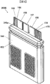
- FIG. 3 (a) and 3 (b) are perspective views of the semiconductor module 300A.
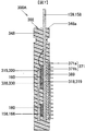
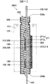
- FIG. 3C is a schematic cross-sectional view of the semiconductor module 300A, which is a schematic cross-sectional view taken along line IVa-IVa in FIG. In FIG. 3C, the reference numerals of the constituent members shown in the cross section taken along the line IVb-IVb are also appended.
- FIG. 4 is a circuit diagram showing a circuit configuration of the semiconductor module 300A.
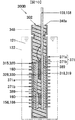
- FIG. 5 is a perspective view of the conductor plate assembly 950 from which the epoxy resin (sealing resin) 348 of the semiconductor module 300A has been removed to facilitate understanding.
- FIG. 6 is a perspective view of the conductor plate assembly 950 from which the first conductor plate 315 and the third conductor plate 320 of FIG. 5 are removed.
- the semiconductor module 300A includes power semiconductor elements (IGBT 328, IGBT 330, diode 156, and diode 166) that constitute the series circuit 150 shown in FIGS. These power semiconductor elements are sealed with a sealing resin made of epoxy resin 348.
- the collector electrode of the IGBT 328 on the upper arm side and the cathode electrode of the diode 156 on the upper arm side are connected via a first conductor plate 315.
- the collector electrode of the IGBT 330 on the lower arm side and the cathode electrode of the diode 166 on the lower arm side are connected via the third conductor plate 320.
- the emitter electrode of the IGBT 328 on the upper arm side and the anode electrode of the diode 156 on the upper arm side are connected via the second conductor plate 318.
- the emitter electrode of the IGBT 330 on the lower arm side and the anode electrode of the diode 166 on the lower arm side are connected via a fourth conductor plate 319.
- the second conductor plate 318 and the third conductor plate 320 are connected by an intermediate electrode 329.
- the power semiconductor elements (IGBT 328, IGBT 330, diode 156, diode 166) have a flat plate-like structure, and each electrode of the power semiconductor element is formed on the front and back surfaces. ing.
- each electrode of the power semiconductor element has a first conductor plate 315 and a second conductor plate 318 or a third conductor plate 320 arranged to face the respective electrode surfaces.
- the fourth conductor plate 319 that is, the first conductor plate 315 and the second conductor plate 318 are stacked so as to face each other substantially in parallel via the IGBT 328 and the diode 156.
- the third conductor plate 320 and the fourth conductor plate 319 have a stacked arrangement facing each other substantially in parallel via the IGBT 330 and the diode 166.
- the third conductor plate 320 and the second conductor plate 318 are connected via an intermediate electrode 329. By this connection, the upper arm circuit and the lower arm circuit are electrically connected to form an upper and lower arm series circuit.
- the first conductor plate 315 on the DC side and the third conductor plate 320 on the AC side are arranged in substantially the same plane.
- the collector electrode of the IGBT 328 on the upper arm side and the cathode electrode of the diode 156 on the upper arm side are fixed.
- the collector electrode of the IGBT 330 on the lower arm side and the cathode electrode of the diode 166 on the lower arm side are fixed.
- the second conductor plate 318 on the AC side and the fourth conductor plate 319 on the DC side are arranged in substantially the same plane.
- the emitter electrode of the IGBT 328 on the upper arm side and the anode electrode of the diode 156 on the upper arm side are fixed to the second conductor plate 318.
- an emitter electrode of the IGBT 330 on the lower arm side and an anode electrode of the diode 166 on the lower arm side are fixed.
- a DC positive terminal 157 extends from the first conductor plate 315.
- An AC terminal 159 extends from the second conductor plate 318.
- a DC negative terminal 158 extends from the fourth conductor plate 319.
- Each of the conductor plates 315, 318, 319, and 320 according to the present embodiment is a wiring for a large current circuit, and is made of a material having high thermal conductivity and low electrical resistance, such as pure copper or copper alloy, and has a thickness of 0. .5 mm or more is preferable.
- each power semiconductor element is joined to each conductor plate 315, 318, 319, 320 via a metal joining material 160.
- the metal bonding material 160 is, for example, a low-temperature sintered bonding material containing a silver sheet or fine metal particles, or lead-free solder having a high thermal conductivity and excellent environmental properties, such as Sn—Cu solder, Sn—Ag. -Cu solder, Sn-Ag-Cu-Bi solder and the like.
- the gate electrode terminals 154 and 164 and the emitter electrode terminals 155 and 165 for connection to the driver circuit 174 are connected to the gate electrode and the emitter electrode of the power semiconductor element by wire bonding, ribbon bonding or the like. It is preferable to use aluminum or gold for the wire or ribbon. Instead of wires or ribbons, connection may be made using solder or the like.
- the gate electrode terminals 154 and 164 and the emitter electrode terminals 155 and 165 are preferably made of pure copper or a copper alloy.
- the DC positive terminal 157, the DC negative terminal 158 and the AC terminal 159, the gate electrode terminals 154 and 164, the emitter electrode terminals 155 and 165, the current detection terminal, the temperature detection terminal, etc. are arranged in a line. These are connected by a tie bar 951 made of an insulating resin or the like at a predetermined interval and are integrally held.
- the semiconductor module 300 ⁇ / b> A includes heat radiating fins 371.
- the heat radiating fin 371 includes a fin plate 371a and a reinforcing plate 371b that increases the rigidity of the fin plate 371a.
- the fin plate 371a has a rectangular flat base and a plurality of columnar fins protruding from one surface of the base.
- the reinforcing plate 371b has a rectangular flat plate shape, and the outer shape of the reinforcing plate 371b is substantially the same as the outer shape of the base portion of the fin plate 371a.
- the base portion of the fin plate 371a and the reinforcing plate 371b are positioned and joined so that the outer peripheral side surface of the base portion of the fin plate 371a and the outer peripheral side surface of the reinforcing plate 371b are flush with each other.
- the semiconductor module 300A is arranged in the case 122.
- the heat radiating fins 371 exchange heat with the refrigerant 121 in the case 122 and radiate heat generated in the semiconductor module to the refrigerant 121.
- the refrigerant 121 flows in a direction orthogonal to the protruding direction from the base of each fin, and circulates in the case 122 by a circulation device (not shown).
- An insulating plate 389 having an insulating property is bonded to the outer surfaces of the second conductor plate 318 and the fourth conductor plate 319 (the surface opposite to the bonding surface of the semiconductor element), and the reinforcing plate 371b is connected to the outer surface of the insulating plate 389. Are joined. After transfer molding described later, the fin plate 371a is joined to the exposed surface of the reinforcing plate 371b. That is, the surface of the fin plate 371a where the fin is formed is exposed from the epoxy resin 348 that is a sealing material.
- the insulating plate 389 is made of an inorganic compound such as an insulating ceramic or an organic compound such as an insulating resin.
- the insulating plate 389 is disposed between the heat radiation fin 371 and the conductor plates 318 and 319 to insulate them.
- the material of the insulating plate 389 is preferably selected to have a high thermal conductivity.
- the insulating plate 389 be connected to the conductor plates 318 and 319 and the reinforcing plate 371b in a state before the resin component is completely cured, that is, in a state having adhesiveness. Note that the insulating plate 389 can be omitted when the reinforcing plate 371b and the fin plate 371a constituting the heat radiation fin 371 are formed of an insulating material.
- the reinforcing plate 371b and the fin plate 371a are made of a metal material such as aluminum, copper, or magnesium, which has a higher thermal conductivity than the epoxy resin 348 used for the sealing resin, or a ceramic material such as alumina.
- a metal material such as aluminum, copper, or magnesium
- a ceramic material such as alumina.
- the material of the reinforcing plate 371b it is preferable to select a material having higher rigidity than the material of the fin plate 371a. In the present embodiment, different materials are selected for the reinforcing plate 371b and the fin plate 371a.
- the second conductor plate 318 or the fourth conductor plate 319, the insulating plate 389, the reinforcing plate 371b, and the fin plate 371a are joined by a method such as welding, soldering, friction stir welding (FSW: Friction Stir Welding). . If the strength of the fin plate 371a is sufficient, the reinforcing plate 371b can be omitted.
- a method such as welding, soldering, friction stir welding (FSW: Friction Stir Welding).
- the second conductor plate 318 and the fourth conductor plate 319 are coupled to the heat radiation fins 371 through the insulating plates 389 so as to be able to conduct heat.
- the heat generated in the semiconductor elements 156, 166, 328, and 330 is transmitted to the second conductor plate 318 or the fourth conductor plate 319, transferred to the heat radiating fin 371 through the insulating plate 389, and radiated from the heat radiating fin 371 to the refrigerant 121.
- the semiconductor structure 302 is formed by molding the conductive plate assembly 950 shown in FIG. 5 with an insulating epoxy resin 348 by a transfer molding method or the like.
- a conductive plate assembly 950 is fixed in a preheated mold, and a power semiconductor is formed by injecting pressure into the mold while melting a thermosetting resin such as an epoxy resin.
- the conductor plate assembly 950 including the elements is sealed with a sealing resin to form a semiconductor structure (module sealing body) 302 shown in FIG.
- the outer surface of the reinforcing plate 371b (the surface opposite to the joint surface with the insulating plate 389) is exposed from the sealing resin 348.
- the sealing resin 348 has a terminal surface 348a in which the terminals 157, 158, 159, 154, 155, 164, and 165 are arranged in a state of being insulated from each other. is doing.
- the surface of the epoxy resin portion was directly fluorinated in a fluorine gas atmosphere to form a first layer 602 having a substitution rate of 0.8 ⁇ m (FIG. 3C). )reference).
- the first layer 602 is formed on the outer surface of the semiconductor structure 302.
- the region where the first layer 602 is formed is a region including the entire contact region of the coolant 121 in the semiconductor structure 302.
- the substitution rate means C—F bond / (C—H bond + C—F bond) in the main chain structure.
- the semiconductor module 300A manufactured in this way is excellent in adhesiveness with internal electronic components to be sealed, such as a conductor plate, since the epoxy resin is not fluorinated at the time of molding.
- 80% of the hydrogen bonded to carbon in the first layer 602 is replaced with fluorine, so that the average free volume in the three-dimensional cross-linked structure is blocked with fluorine, thereby preventing the refrigerant from entering.
- the conductive plate assembly 950 is molded, if a hydrophobic group is introduced into the sealing resin, it becomes easy to repel water and poor wettability with internal electronic components to be sealed such as diodes, IGBTs, and conductive plates. The problem that the adhesive force with them is weak arises.
- a sealing resin is used as an insulator, when it is heat-cured, peeling from the conductor and voids are generated in the sealing molded body, and moisture accumulates starting from them, resulting in a decrease in insulation. May happen.
- the epoxy resin used for integral molding in the present invention is not particularly limited as long as it is a thermosetting resin composition that can be sealed and molded, but preferably contains an epoxy resin, a curing agent, a curing accelerator, and an inorganic filler as essential components.
- An epoxy resin composition is desirable.
- the fluorine atoms are changed so that the length calculated by the cube root of the average free volume in the three-dimensional crosslinked structure of the first layer 602 is smaller than the length of the longest side of the molecules constituting the refrigerant.
- it is not particularly limited as long as it is a substitutable element.
- an element having water repellency is more preferable when replaced.
- halogen elements such as fluorine, bromine, chlorine, and iodine can be used.
- the glass transition temperature of the resin having the three-dimensional crosslinked structure of the first layer 602 is desirably 50 ° C. or higher. Although it depends on the operating temperature range of the electronic device, when the glass transition temperature is exceeded, the three-dimensional crosslinked structure is easily moved by heat (rubber state). For this reason, even if the average free volume is blocked with an element such as fluorine, there is a possibility that the refrigerant cannot be prevented from entering.
- the glass transition temperature of the resin having the three-dimensional cross-linked structure of the first layer 602 is preferably 130 ° C. or higher.
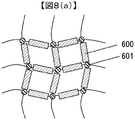
- FIG. 8A shows a model of a three-dimensional crosslinked structure.
- the main chain 600 of the resin is connected by a crosslinking point 601.
- it has a three-dimensional network structure like a mesh.
- FIGS. 8B and 8C for easy understanding, only one of them is taken up in FIGS. 8B and 8C, and fluorination treatment will be described as an example.
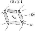
- FIG. 8B is a schematic diagram of the three-dimensional curable resin before the fluorination treatment.
- the structure of the main chain 600 of the resin includes hydrogen bonded to carbon which is the main chain skeleton.
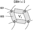
- FIG. 8C is a schematic diagram of the three-dimensional curable resin after the fluorination treatment.
- hydrogen bonded to carbon which is the main chain skeleton is replaced with fluorine which is a larger element than hydrogen, so that the average free volume V 0 becomes V 1 ,
- the average free volume V 1 after the processing is smaller than that before the processing (V 0 ).
- the voids that were vacant before the treatment are blocked by fluorine.
- the higher the substitution rate the smaller the average free volume. Therefore, in order to prevent the refrigerant from entering, it is effective to increase the degree of the substitution rate.
- the length that is calculated by the cube root of the average free volume in the three-dimensional crosslinked structure constitutes the refrigerant. If the length is smaller than the length of the longest side, the waterproof property can be improved.
- the semiconductor module 300A includes the semiconductor elements 328, 330, 156, and 166, the conductor plates 318 and 319 to which the semiconductor elements are joined, the conductor plates 318 and 319, and the insulating plate on the semiconductor elements.
- a semiconductor structure 302 including a heat dissipating fin 371 fixed to be thermally conductive via 389, an epoxy resin 348 that exposes one surface of the heat dissipating fin 371 and seals the semiconductor element, and at least in a contact region of the refrigerant 121 And a first layer 602 that covers the boundary with the epoxy resin 348.
- the first layer 602 having a three-dimensional crosslinked structure has a length calculated by the root of the mean free volume in the three-dimensional crosslinked structure so that the length is smaller than the length of the longest side of the molecules constituting the refrigerant.
- One layer 602 is plugged with elements.
- the refrigerant 121 can be prevented from entering the sealing resin 348, so that the life of the semiconductor module 300A can be extended. Even if the refrigerant is not completely covered by the element and the refrigerant has entered, if it is smaller than the length of the longest side of the molecule that constitutes the refrigerant, the degree of freedom is reduced and the pressure required for infiltration is generated. improves.
- FIG. 9 is a view similar to FIG. 3A and is a perspective view of a semiconductor module 300B according to the second embodiment.
- FIG. 10 is a diagram similar to FIG. 3C and is a schematic cross-sectional view of a semiconductor module 300B according to the second embodiment.
- the same or corresponding parts as those in the first embodiment are denoted by the same reference numerals, and description thereof is omitted.
- differences from the first embodiment will be described in detail.
- the radiating fins 371 are provided only on one surface of the semiconductor module 300A.
- the radiating fins 371 are provided on both surfaces of the semiconductor module 300B. Is provided.
- an insulating plate 389 having insulating properties is joined to the outer surfaces of the first conductor plate 315 and the third conductor plate 320.
- a reinforcing plate 371 b is joined to the outer surface of the insulating plate 389.
- the fin plate 371a is joined to the exposed surface of the reinforcing plate 371b.
- the insulating plate 389 is made of an inorganic compound such as insulating ceramics or an organic compound such as insulating resin, and is disposed between the radiation fins 371 and the conductor plates 315 and 320 to insulate them.
- the material of the insulating plate 389 is preferably selected to have a high thermal conductivity.
- the insulating plate 389 When the insulating plate 389 is formed of resin, it is preferable to connect to the conductor plates 315 and 320 and the reinforcing plate 371b in a state before the resin component is completely cured, that is, in a state having adhesiveness. Note that the insulating plate 389 can be omitted when the reinforcing plate 371b and the fin plate 371a constituting the heat radiation fin 371 are formed of an insulating material.
- the reinforcing plate 371b and the fin plate 371a are made of a metal material having a higher thermal conductivity than a material used for the sealing resin 348, such as aluminum, copper, or magnesium, or a ceramic material such as alumina.
- a material used for the sealing resin 348 such as aluminum, copper, or magnesium
- a ceramic material such as alumina.
- the first conductor plate 315 or the third conductor plate 320, the insulating plate 389, the reinforcing plate 371b, and the fin plate 371a are joined by welding, soldering, friction stir welding, or the like. If the strength of the fin plate 371a is sufficient, the reinforcing plate 371b can be omitted.
- the same effects as those of the first embodiment can be obtained.
- the cooling performance can be improved as compared with the first embodiment.
- FIG. 11 is a view similar to FIG. 3C and is a schematic cross-sectional view of a semiconductor module 300C according to the third embodiment.
- the same or corresponding parts as those in the first embodiment are denoted by the same reference numerals, and description thereof is omitted.
- differences from the first embodiment will be described in detail.
- each terminal is arranged on one terminal surface 348a.
- a surface opposite to the one terminal surface 348a hereinafter, another terminal surface 348b.
- a DC negative terminal 158, a DC positive terminal 157 and an AC terminal 159, gate electrode terminals 154 and 164, and emitter electrode terminals 155 and 165 shown in FIG. 4 extend from one terminal surface 348a.
- the current detection terminal 190 extends from the other terminal surface 348b.
- the two terminal surfaces 348a and 348b are exposed. That is, since the first layer 602 is not formed on the two terminal surfaces 348a and 348b, the area where the first layer 602 is not formed is increased as compared with the first embodiment.
- the two terminal surfaces 348a and 348b and the terminals are covered with a curing member, the first layer 602 is formed with a coating solution, and the curing member is removed.
- the same operational effects as those of the first embodiment can be obtained. Since the area where the first layer 602 is formed is smaller than that in the first embodiment, the cost and weight can be reduced as compared with the first embodiment.
- a dimethylformamide solution of 20% by weight polyamic acid is prepared, and then the surface of the semiconductor structure 302 is coated using this coating solution.
- the polyimide of the first layer 602 is formed by heating and curing at 100 ° C. and 150 ° C. for 1 hour, respectively.
- the first layer carbon and the first layer carbon so that the length calculated by the cube root of the mean free volume in the three-dimensional crosslinked structure is smaller than the length of the longest side of the molecules constituting the refrigerant. A part of the hydrogen to be bonded was replaced with fluorine.
- the example which forms the 1st layer 602 by the dip method immersed in a coating solution was demonstrated, this invention is not limited to this.
- the method of applying the coating solution is not limited to immersion, and the first layer 602 may be formed by applying the coating solution to the semiconductor structure 302 by spraying or brushing. Dip (dipping), spraying, brushing, or combinations thereof can also be used. If the embeddability is insufficient, it can be improved by overcoating. (Modification 2)
- the example in which the first layer 602 is formed in a region including the entire contact region of the coolant 121 in the semiconductor structure 302 has been described; however, the present invention is not limited to this.
- the first layer 602 may be formed inside the epoxy resin portion instead of the surface of the epoxy resin portion that seals the conductor or the like.
- Modification 3 In the above-described embodiment, an example in which the first layer 602 is formed by directly fluorinating an epoxy resin as a sealing material using a fluorine gas is described, but the present invention is not limited to this.
- the first layer 602 may be formed by surface fluorination treatment by radical reaction. For example, after adjusting a solution that undergoes a fluorinated radical reaction at a certain concentration, the semiconductor structure 302 is immersed in this coating solution and coated. Thereafter, a part of the main chain skeleton was fluorinated by heat treatment at 100 ° C. for 3 hours.
- (Modification 4) In the above-described embodiment, the example in which the first layer 602 is formed in the entire contact region of the coolant 121 in the sealing resin 348 has been described, but the present invention is not limited to this.
- the first layer 602 may be provided so as to cover at least the boundary between the sealing resin 348 and the radiation fin 371. Thereby, by coating the boundary with the different member, the refrigerant is prevented from entering from the boundary with the different member, and the waterproof property is improved.
- (Modification 5) In the above-described embodiment, the example in which the first layer 602 is formed in the entire contact region of the coolant 121 in the sealing resin 348 has been described, but the present invention is not limited to this.
- the first layer 602 may be provided in the entire region in contact with the refrigerant 121 in the sealing resin 348 and the radiation fins 371.
- the pinholes and ridges of the fin portion are covered, and the waterproof property is excellent and long-term reliability is ensured. I can do it.
- the present invention is not limited to the above-described embodiments, and other forms conceivable within the scope of the technical idea of the present invention are also included in the scope of the present invention. .
Landscapes
- Engineering & Computer Science (AREA)
- Microelectronics & Electronic Packaging (AREA)
- Physics & Mathematics (AREA)
- Thermal Sciences (AREA)
- Power Engineering (AREA)
- Cooling Or The Like Of Semiconductors Or Solid State Devices (AREA)
- Inverter Devices (AREA)
- Structures Or Materials For Encapsulating Or Coating Semiconductor Devices Or Solid State Devices (AREA)
Abstract
電子装置における防水効果の向上を図る。 電子部品315、320と、前記電子部品を封止するエポキシ樹脂部348と、を備え、前記電子部品を冷却する冷媒121中に配置される電子装置300Aであって、エポキシ樹脂部348は、表面又は内部において、三次元架橋構造を有する第1層602が形成される。第1層602は、当該第1層の前記三次元架橋構造における平均自由体積の三乗根により算出される長さが前記冷媒を構成する分子の最長辺の長さよりも小さくなるように、形成される。
Description
本発明は、搭載された電子部品を冷却する機能を具備した電子装置に関する。
近年、地球温暖化防止のため、自然エネルギーを有効利用した洋上風力発電が注目されている。風力発電には、風車の回転を電力に変換するための電力変換用モジュールやモータの制御装置用などの低圧系モジュールに代表される半導体装置が必要となる。電力変換装置は、効率の高いパワー半導体のスイッチングを用いる方式が主流であり、半導体素子をゲルや樹脂で封止し絶縁保護している。洋上の雰囲気は、陸上に比べ湿度が高く、塩分を多く含んでいるため、より防湿性や防水性に優れた電力変換装置や制御装置が求められている。
また、省エネルギー化の推進や低炭素社会の実現のため、電気自動車やハイブリッド自動車といった自動車の電動化が急速に進展している。特に、電動化システムの基本構成要素となるインバータの役割は今まで以上に多様化し、小型化と高出力化を同時に実現することが求められている。インバータには、その主要部品としてトランジスタやダイオード等のパワー半導体チップを樹脂で封止してなるパワー半導体モジュールが搭載されている。電気自動車、ハイブリッド自動車用のパワー半導体モジュールでは、デバイスの電流容量の増大や小型化による電流密度の増大に伴い、通電により発熱するため、パワー半導体モジュールの温度上昇を抑える冷却手段が設けられている。冷却手段としては、水や油、有機溶媒などを用いた冷媒循環方式が主流であり、冷媒に対する防水構造が必要とされる。
電子部品や電力ケーブル等で導体を覆うために用いる樹脂として、エポキシ樹脂が知られている(特許文献1参照)。特許文献1には、エポキシ樹脂の分岐鎖にアルキル基などの疎水基を導入することで、従来よりも吸水性が低く、耐水性を高めることが記載されている。
疎水基を有するエポキシ樹脂は、半導体素子や配線、電線等の導体との濡れ性が悪く、密着力が弱いという問題点がある。このようなエポキシ樹脂を絶縁体として用いると、加熱硬化させた際に、導体からの剥離や、成型物内にボイドが発生し、それらを起点として水分が溜まり、絶縁性の低下が起こる恐れがある。
本発明は、絶縁性などの信頼性を損なうことなく、水や油、有機溶媒などの冷媒浸入の防止を可能とする電子装置の提供を課題とする。
本発明の電子装置は、電子部品と、電子部品を封止するエポキシ樹脂部と、を備え、電子部品を冷却する冷媒中に配置される電子装置であって、エポキシ樹脂部は、エポキシ樹脂部の表面又は内部において、第1層が形成され、第1層は、三次元架橋構造を有し、前記三次元架橋構造における平均自由体積の三乗根により算出される長さが冷媒を構成する分子の最長辺の長さよりも小さくなるように、形成されることを特徴とする。
本発明によれば、冷媒の浸入を防止し、防水効果の向上を図ることができる。
以下、図面を参照して本願発明に係る実施形態について説明する。
図1は、ハイブリッド自動車の制御ブロックを示す図である。エンジンEGNおよびモータジェネレータMG1は車両の走行用トルクを発生する。モータジェネレータMG1は回転トルクを発生するだけでなく、モータジェネレータMG1に外部から加えられる機械エネルギーを電力に変換する機能を有する。
モータジェネレータMG1は、たとえば同期機あるいは誘導機であり、上述のごとく、運転方法によりモータとしても発電機としても動作する。モータジェネレータMG1を自動車に搭載する場合には、小型で高出力を得ることが望ましく、ネオジウムなどの磁石を使用した永久磁石型の同期電動機が適している。永久磁石型の同期電動機は誘導電動機に比べて回転子の発熱が少なく、この観点でも自動車用として優れている。
エンジンEGNの出力トルクは動力分配機構TSMを介してモータジェネレータMG1に伝達され、動力分配機構TSMからの回転トルクあるいはモータジェネレータMG1が発生する回転トルクは、トランスミッションTMおよびデファレンシャルギアDIFを介して車輪に伝達される。一方、回生制動の運転時には、車輪から回転トルクがモータジェネレータMG1に伝達され、供給されてきた回転トルクに基づいて交流電力を発生する。発生した交流電力は後述するように電力変換装置200により直流電力に変換され、高電圧用のバッテリ136を充電し、充電された電力は再び走行エネルギーとして使用される。
次に半導体素子のスイッチング動作によって電力を直流から交流に、交流から直流に変換する電力変換装置200について説明する。インバータ回路140は、バッテリ136と直流コネクタ138を介して電気的に接続されており、バッテリ136とインバータ回路140との相互において電力の授受が行われる。モータジェネレータMG1をモータとして動作させる場合には、インバータ回路140は直流コネクタ138を介してバッテリ136から供給された直流電力に基づき交流電力を発生し、交流端子188を介してモータジェネレータMG1に供給する。モータジェネレータMG1とインバータ回路140からなる構成は電動発電ユニットとして動作する。
なお、本実施形態では、バッテリ136の電力によって電動発電ユニットを電動ユニットとして作動させることにより、モータジェネレータMG1の動力のみによって車両の駆動ができる。さらに、本実施形態では、電動発電ユニットを発電ユニットとしてエンジンEGNの動力あるいは車輪からの動力によって作動させて発電させることにより、バッテリ136の充電ができる。
電力変換装置200は、インバータ回路140に供給される直流電力を平滑化するためのコンデンサモジュール500を備えている。
電力変換装置200は、上位の制御装置から指令を受けたりあるいは上位の制御装置に状態を表すデータを送信したりするための通信用のコネクタ21を備えている。電力変換装置200は、コネクタ21からの指令に基づいて制御回路172でモータジェネレータMG1の制御量を演算し、さらにモータとして運転するか発電機として運転するかを演算し、演算結果に基づいて制御パルスを発生し、その制御パルスをドライバ回路174へ供給する。ドライバ回路174は、供給された制御パルスに基づいて、インバータ回路140を制御するための駆動パルスを発生する。
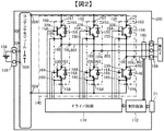
次に、図2を用いてインバータ回路140の電気回路の構成を説明する。なお、本実施形態では半導体素子として絶縁ゲート型バイポーラトランジスタ(Insulated Gate Bipolar Transistor)を使用しており、以下略してIGBTと記す。
上アームのIGBT328およびダイオード156と、下アームのIGBT330およびダイオード166とで、上下アームの直列回路150が構成される。インバータ回路140は、この直列回路150を、出力しようとする交流電力のU相、V相、W相の3相に対応して備えている。
これらの3相は、この実施の形態ではモータジェネレータMG1の電機子巻線の3相の各相巻線に対応している。3相のそれぞれの上下アームの直列回路150は、直列回路の中点部分である中間電極169から交流電流を出力する。この中間電極169は、交流端子159および交流端子188を通して、モータジェネレータMG1への交流電力線である交流バスバー802と接続される。
上アームのIGBT328のコレクタ電極は、直流正極端子157を介してコンデンサモジュール500の正極側のコンデンサ端子506に電気的に接続されている。また、下アームのIGBT330のエミッタ電極は、直流負極端子158を介してコンデンサモジュール500の負極側のコンデンサ端子504に電気的に接続されている。
上述のように、制御回路172は上位の制御装置からコネクタ21を介して制御指令を受け、これに基づいてインバータ回路140を構成する各相の直列回路150の上アームあるいは下アームを構成するIGBT328やIGBT330を制御するための制御信号である制御パルスを発生し、ドライバ回路174に供給する。
ドライバ回路174は、上記制御パルスに基づき、各相の直列回路150の上アームあるいは下アームを構成するIGBT328やIGBT330を制御するための駆動パルスを各相のIGBT328やIGBT330に供給する。IGBT328やIGBT330は、ドライバ回路174からの駆動パルスに基づき、導通あるいは遮断動作を行い、バッテリ136から供給された直流電力を三相交流電力に変換し、この変換された電力はモータジェネレータMG1に供給される。
上アームのIGBT328および下アームのIGBT330は、それぞれ、コレクタ電極と、信号用のエミッタ電極と、ゲート電極とを備えている。上アームのダイオード156が、コレクタ電極端子153とエミッタ電極端子155との間に電気的に接続されている。また、ダイオード166が、コレクタ電極端子163とエミッタ電極端子165との間に電気的に接続されている。
なお、スイッチング用パワー半導体素子としては金属酸化物半導体型電界効果トランジスタ(以下略してMOSFETと記す)を用いてもよい、この場合はダイオード156やダイオード166は不要となる。スイッチング用パワー半導体素子としては、IGBTは直流電圧が比較的高い場合に適していて、MOSFETは直流電圧が比較的低い場合に適している。
コンデンサモジュール500は、正極側のコンデンサ端子506と負極側のコンデンサ端子504と正極側の電源端子509と負極側の電源端子508とを備えている。バッテリ136からの高電圧の直流電力は、直流コネクタ138を介して、正極側の電源端子509や負極側の電源端子508に供給され、コンデンサモジュール500の正極側のコンデンサ端子506および負極側のコンデンサ端子504から、インバータ回路140へ供給される。
一方、交流電力からインバータ回路140によって変換された直流電力は、正極側のコンデンサ端子506や負極側のコンデンサ端子504からコンデンサモジュール500に供給され、正極側の電源端子509や負極側の電源端子508から直流コネクタ138を介してバッテリ136に供給され、バッテリ136に蓄積される。
制御回路172は、IGBT328およびIGBT330のスイッチングタイミングを演算処理するためのマイクロコンピュータ(以下、「マイコン」と記述する)を備えている。マイコンへの入力情報としては、モータジェネレータMG1に対して要求される目標トルク値、直列回路150からモータジェネレータMG1に供給される電流値、およびモータジェネレータMG1の回転子の磁極位置がある。
目標トルク値は、不図示の上位の制御装置から出力された指令信号に基づくものである。電流値は、電流センサ180による検出信号に基づいて検出されたものである。磁極位置は、モータジェネレータMG1に設けられたレゾルバなどの回転磁極センサ(不図示)から出力された検出信号に基づいて検出されたものである。本実施形態では、電流センサ180は3相の電流値を検出する場合を例に挙げているが、2相分の電流値を検出するようにし、演算により3相分の電流を求めてもよい。
制御回路172内のマイコンは、目標トルク値に基づいてモータジェネレータMG1のd軸、q軸の電流指令値を演算し、この演算されたd軸、q軸の電流指令値と、検出されたd軸、q軸の電流値との差分に基づいてd軸、q軸の電圧指令値を演算し、この演算されたd軸、q軸の電圧指令値を、検出された磁極位置に基づいてU相、V相、W相の電圧指令値に変換する。そして、マイコンは、U相、V相、W相の電圧指令値に基づく基本波(正弦波)と搬送波(三角波)との比較に基づいてパルス状の変調波を生成し、この生成された変調波をPWM(パルス幅変調)信号としてドライバ回路174に出力する。
ドライバ回路174は、下アームを駆動する場合、PWM信号を増幅したドライブ信号を、対応する下アームのIGBT330のゲート電極に出力する。また、ドライバ回路174は、上アームを駆動する場合、PWM信号の基準電位のレベルを上アームの基準電位のレベルにシフトしてからPWM信号を増幅し、これをドライブ信号として、対応する上アームのIGBT328のゲート電極にそれぞれ出力する。
直列回路150に設けられた温度センサ(不図示)からは直列回路150の温度の情報がマイコンに入力されている。また、マイコンには直列回路150の直流正極側の電圧の情報が入力されている。マイコンは、それらの情報に基づいて過温度検知および過電圧検知を行い、過温度あるいは過電圧が検知された場合には全てのIGBT328、IGBT330のスイッチング動作を停止させる。
図3~図6を参照して、インバータ回路140に使用される半導体モジュール300a~300cの構成を説明する。なお、上記半導体モジュール300a~300c(図2参照)はいずれも同じ構造であるため、代表して半導体モジュール300a(以下、半導体モジュール300Aと記す)の構造を説明する。
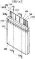
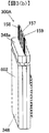
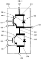
図3(a)及び図3(b)は、半導体モジュール300Aの斜視図である。図3(c)は、半導体モジュール300Aの断面模式図であり、図3(a)のIVa-IVa線で切断した断面模式図である。なお、図3(c)では、IVb-IVb線で切断した断面において表される構成部材の符号についても付記している。図4は、半導体モジュール300Aの回路構成を示す回路図である。図5は、理解を助けるために、半導体モジュール300Aのエポキシ樹脂(封止樹脂)348を取り除いた導体板組み950の斜視図である。図6は、図5の第1導体板315および第3導体板320を取り除いた導体板組み950の斜視図である。
図3(c)に示すように、半導体モジュール300Aは、図2および図4に示す直列回路150を構成するパワー半導体素子(IGBT328、IGBT330、ダイオード156、ダイオード166)を含んで構成される。これらパワー半導体素子は、エポキシ樹脂348からなる封止樹脂により封止されてなる。
図4を参照して半導体モジュールの回路構成について説明する。図4に示すように、上アーム側のIGBT328のコレクタ電極と上アーム側のダイオード156のカソード電極は、第1導体板315を介して接続されている。同様に、下アーム側のIGBT330のコレクタ電極と下アーム側のダイオード166のカソード電極は、第3導体板320を介して接続されている。上アーム側のIGBT328のエミッタ電極と上アーム側のダイオード156のアノード電極は、第2導体板318を介して接続されている。同様に、下アーム側のIGBT330のエミッタ電極と下アーム側のダイオード166のアノード電極は、第4導体板319を介して接続されている。第2導体板318と第3導体板320は中間電極329によって接続されている。こうした回路構成により上下アームの直列回路150が形成される。
図3(c)および図6に示すように、パワー半導体素子(IGBT328、IGBT330、ダイオード156、ダイオード166)は、板状の扁平構造であり、当該パワー半導体素子の各電極は表裏面に形成されている。
図3(c)および図5に示すように、パワー半導体素子の各電極は、それぞれの電極面に対向して配置される第1導体板315と第2導体板318、または第3導体板320と第4導体板319によって挟まれる。つまり、第1導体板315と第2導体板318は、IGBT328およびダイオード156を介して略平行に対向した積層配置となる。同様に、第3導体板320と第4導体板319は、IGBT330およびダイオード166を介して略平行に対向した積層配置となる。図5に示すように、第3導体板320と第2導体板318は中間電極329を介して接続されている。この接続により上アーム回路と下アーム回路が電気的に接続され、上下アーム直列回路が形成される。
直流側の第1導体板315と交流側の第3導体板320は、略同一平面状に配置される。第1導体板315には、上アーム側のIGBT328のコレクタ電極と上アーム側のダイオード156のカソード電極が固着される。第3導体板320には、下アーム側のIGBT330のコレクタ電極と下アーム側のダイオード166のカソード電極が固着される。同様に、交流側の第2導体板318と直流側の第4導体板319は、略同一平面状に配置される。第2導体板318には、上アーム側のIGBT328のエミッタ電極と上アーム側のダイオード156のアノード電極が固着される。第4導体板319には、下アーム側のIGBT330のエミッタ電極と下アーム側のダイオード166のアノード電極が固着される。
第1導体板315からは直流正極端子157が延在している。第2導体板318からは交流端子159が延在している。第4導体板319からは直流負極端子158が延在している。
本実施の形態に係る各導体板315、318、319、320は、大電流回路用配線であり、純銅もしくは銅合金等の熱伝導率が高くて電気抵抗の低い材料からなり、厚さは0.5mm以上がよい。
図3(c)に示すように、各導体板315、318、319、320には各パワー半導体素子が金属接合材160を介してそれぞれ接合されている。金属接合材160は、たとえば銀シートや微細金属粒子を含んだ低温焼結接合材、あるいは、熱伝導率が高くて環境性に優れた鉛フリーはんだ等、たとえば、Sn-Cuはんだ、Sn-Ag-Cuはんだ、Sn-Ag-Cu-Biはんだ等である。
ドライバ回路174と接続するためのゲート電極端子154、164およびエミッタ電極端子155、165は、ワイヤボンディング、リボンボンディング等により、パワー半導体素子のゲート電極およびエミッタ電極に接続されている。ワイヤやリボンにはアルミニウムや金を用いることが好適である。ワイヤやリボンに代えて、はんだ等を用いて接続してもよい。ゲート電極端子154、164およびエミッタ電極端子155、165は、純銅もしくは銅合金を用いることが好適である。なお、直流正極端子157、直流負極端子158および交流端子159、ならびに、ゲート電極端子154、164およびエミッタ電極端子155、165、その他、電流検出用端子、温度検出用端子等は、一列に配置され、所定の間隔で絶縁性樹脂等からなるタイバー951により接続され、一体的に保持されている。
図3(c)および図5に示すように、半導体モジュール300Aは、放熱フィン371を備えている。図3(c)に示すように、放熱フィン371は、フィン板371aと、フィン板371aの剛性を高める補強板371bとを有している。フィン板371aは矩形平板状の基部と、基部の一面に突設された円柱状の複数のフィンとを有している。補強板371bは矩形平板状であり、補強板371bの外形はフィン板371aの基部の外形と略同一とされている。フィン板371aの基部と補強板371bとは、フィン板371aの基部の外周側面と補強板371bの外周側面とが面一となるように位置決めされ、接合される。
半導体モジュール300Aは、ケース122内に配置される。放熱フィン371は、ケース122内の冷媒121との間で熱交換を行い、半導体モジュールで発生した熱を冷媒121に放熱する。冷媒121は、各フィンの基部からの突出方向と直交する方向に流れ、図示しない循環装置によりケース122内を循環する。
第2導体板318および第4導体板319の外側面(半導体素子の接合面の反対側の面)には絶縁性を有する絶縁板389が接合され、絶縁板389の外側面には補強板371bが接合される。後述のトランスファーモールド成形の後、補強板371bの露出面にフィン板371aが接合される。つまり、フィン板371aにおけるフィンが形成される面は封止材であるエポキシ樹脂348から露出する。絶縁板389は、絶縁性を有するセラミックスなどの無機化合物や絶縁性を有する樹脂などの有機化合物からなる。絶縁板389は、放熱フィン371と導体板318、319との間に配置されて、両者を絶縁する。絶縁板389の材質は、熱伝導率の高いものを選択することが好ましい。絶縁板389を樹脂で形成する場合、樹脂成分が完全に硬化する前の状態、すなわち粘着性を有する状態で導体板318、319、および、補強板371bに接続することが好ましい。なお、放熱フィン371を構成する補強板371bやフィン板371aが絶縁性を有する材料で形成される場合は、絶縁板389を省略することができる。
補強板371bおよびフィン板371aは、アルミニウム、銅、マグネシウムなど、封止樹脂に用いられるエポキシ樹脂348に比べて熱伝導率の高い金属材料やアルミナなどのセラミックス材料からなる。補強板371bの材質は、フィン板371aの材質よりも剛性の高い材質を選択することが好適である。本実施の形態では、補強板371bとフィン板371aとは異なる材質が選択されている。
第2導体板318または第4導体板319と、絶縁板389と、補強板371bと、フィン板371aとは、溶接、はんだ、摩擦攪拌接合(FSW:Friction Stir Welding)などの方法により接合される。なお、フィン板371aの強度が十分な場合には、補強板371bを省略することができる。
このように第2導体板318および第4導体板319は、それぞれ絶縁板389を介して放熱フィン371に熱伝導可能に結合されている。半導体素子156、166、328、330で発生した熱は、第2導体板318または第4導体板319に伝わり、絶縁板389を介して放熱フィン371に伝わり、放熱フィン371から冷媒121に放熱される。
第1の実施の形態における半導体モジュール300Aの製造方法について説明する。まず、図5にて示される導体板組み950をトランスファーモールド法などにより、絶縁性を有するエポキシ樹脂348でモールドすることで半導体構造体302が形成される。トランスファーモールド法では、導体板組み950を予め加熱された金型内に固定し、金型内にエポキシ系樹脂などの熱硬化性樹脂を溶融させながら加圧注入して成形することで、パワー半導体素子を含む導体板組み950が封止樹脂により封止され、図7に示される半導体構造体(モジュール封止体)302が形成される。なお、トランスファーモールドを行う際、補強板371bの外側面(絶縁板389との接合面の反対側の面)は封止樹脂348より露出される。図3および図3(c)に示すように、封止樹脂348は、各端子157、158、159、154、155、164、165が相互に絶縁された状態で配置される端子面348aを有している。
続いて、半導体構造体302を反応管にセットした後、フッ素ガス雰囲気下、エポキシ樹脂部の表面を直接フッ素化し、置換率0.8の第1層602を約5μm形成した(図3(c)参照)。本実施例の形態では、半導体構造302の外表面に、第1層602を形成している。第1層602が形成される領域は、半導体構造体302における冷媒121の接触領域の全体を含む領域である。ここで置換率とは、主鎖構造においてC-F結合/(C-H結合+C-F結合)を意味する。
このようにして製造された半導体モジュール300Aは、モールド成形時には、エポキシ樹脂はフッ素化されていないことから、導体板などの封止する内部電子部品との密着性に優れている。また、第1層602の炭素と結合される水素の8割がフッ素に置換されたことで、三次元架橋構造における平均自由体積がフッ素で塞がり、冷媒の浸入を防止できる。
一方、導体板組み950をモールド成形する際に、封止樹脂に疎水基が導入されていると撥水しやすくなり、ダイオードやIGBT、導体板など封止させる内部電子部品との濡れ性が悪く、それらとの密着力が弱いという問題点が生じてしまう。このような封止樹脂を絶縁体として用いると、加熱硬化させた際に、導体などからの剥離や、封止成型体内にボイドが発生し、それらを起点として水分が溜まり、絶縁性の低下が起こる恐れがある。
本発明において一体成型に用いるエポキシ樹脂は、封止成形できる熱硬化性樹脂組成物であれば特に制限されないが望ましくはエポキシ樹脂、硬化剤、硬化促進剤、並びに無機質充填剤を必須成分とする、エポキシ樹脂組成物が望ましい。
本実施例では、第1層602の三次元架橋構造における平均自由体積の三乗根により算出される長さが前記冷媒を構成する分子の最長辺の長さよりも小さくなるように、フッ素原子を選択したが、置換可能な元素であれば特に制限されない。冷媒の浸入を防ぐ点では、置換した際に、撥水性を有する元素がさらに好ましい。例えば、フッ素、臭素、塩素、ヨウ素といったハロゲン元素が挙げられる。
第1層602の三次元架橋構造を有する樹脂のガラス転移温度は、50℃以上が望ましい。電子装置の使用温度範囲にもよるが、ガラス転移温度以上になると、三次元架橋構造が熱により動きやすく(ゴム状態)なる。このため、フッ素などの元素で、平均自由体積を塞いだとしても、冷媒の浸入を防げなくなる恐れがある。ハイブリッド自動車用のインバータ用などの高圧系モジュールなどに代表される半導体装置では、第1層602の三次元架橋構造を有する樹脂のガラス転移温度は130℃以上が好ましい。
図8を用いて、第1層の3次元硬化構造の形成について説明する。図8(a)には、三次元架橋構造のモデルを示す。図8(a)に示すように、3次元の硬化性樹脂は、樹脂の主鎖600が架橋点601によって連結している。実際は、メッシュのように3次元の網目構造であるが、わかりやすいように、図8(b)や(c)ではこのうちの1つのみを取り上げ、フッ素化処理を例に説明する。図8(b)は、フッ素化処理前の3次元硬化性樹脂の模式図である。樹脂の主鎖600の構造には、主鎖骨格である炭素に結合している水素も含まれている。樹脂の主鎖600と架橋点601で囲まれた網目構造内の空隙が、フッ素処理前の平均自由体積V0である。図8(c)は、フッ素化処理後の3次元硬化性樹
脂の模式図である。樹脂の主鎖600の構造には、主鎖骨格である炭素と結合していた水素が、水素に比べて大きな元素であるフッ素に置換されることで、平均自由体積V0はV1となり、処理前(V0)に比べて処理後の平均自由体積V1は小さくなる。
脂の模式図である。樹脂の主鎖600の構造には、主鎖骨格である炭素と結合していた水素が、水素に比べて大きな元素であるフッ素に置換されることで、平均自由体積V0はV1となり、処理前(V0)に比べて処理後の平均自由体積V1は小さくなる。
即ち、処理前に空いていた空隙が、フッ素により塞がれることになる。置換率が高い程、平均自由体積が小さくなることから、冷媒の浸入を防ぐためには、置換率の度合いを高めることが有効である。また、第1層602の平均自由体積が、ハロゲンなどの元素によって完全に塞ぎきれなくても、三次元架橋構造における平均自由体積の三乗根により算出される長さが前記冷媒を構成する分子の最長辺の長さよりも小さくなれば、防水性が向上できる。これは、冷媒が浸入したとしても、冷媒を構成する分子の最長辺の長さよりも小さければ、自由度が減じて、浸入に必要な圧力が生じるため、導体を封止している内部まで侵入することが出来ないためである。
上述した第1の実施の形態に係る半導体モジュール300Aは、半導体素子328、330、156、166と、半導体素子が接合された導体板318、319と、半導体素子に導体板318、319および絶縁板389を介して熱伝導可能に固着された放熱フィン371と、放熱フィン371の一面を露出して半導体素子を封止するエポキシ樹脂348とを備える半導体構造体302と、少なくとも冷媒121の接触領域内におけるエポキシ樹脂348との境界を覆う第1層602とを備える。
三次元架橋構造を有する第1層602は、三次元架橋構造における平均自由体積の三乗根により算出される長さが、冷媒を構成する分子の最長辺の長さよりも小さくなるように、第1層602の元素で塞がれている。
第1層602を形成することによって、冷媒121が封止樹脂348内に浸入することを防止することができるため、半導体モジュール300Aの長寿命化を図ることができる。仮に、完全に元素で塞ぎきれず、冷媒が浸入したとしても、冷媒を構成する分子の最長辺の長さよりも小さければ、自由度が減じて、浸入に必要な圧力が生じるため、防水性は向上する。
図9および図10を参照して第2の実施の形態に係る半導体モジュール300Bについて説明する。図9は、図3(a)と同様の図であり、第2の実施の形態に係る半導体モジュール300Bの斜視図である。図10は、図3(c)と同様の図であり、第2の実施の形態に係る半導体モジュール300Bの断面模式図である。図中、第1の実施の形態と同一もしくは相当部分には同一符号を付し、説明を省略する。以下、第1の実施の形態との相違点について詳しく説明する。
第1の実施の形態では、放熱フィン371が半導体モジュール300Aの一方の面にのみ設けられている例について説明したが、第2の実施の形態では、半導体モジュール300Bの両方の面に放熱フィン371が設けられている。
図10に示すように、第1導体板315および第3導体板320の外側面には絶縁性を有する絶縁板389が接合される。絶縁板389の外側面には、補強板371bが接合される。トランスファーモールド成形の後、補強板371bの露出面にフィン板371aが接合される。絶縁板389は、絶縁性を有するセラミックスなどの無機化合物や絶縁性を有する樹脂などの有機化合物からなり、放熱フィン371と導体板315、320との間に配置されて、両者を絶縁する。絶縁板389の材質は、熱伝導率の高いものを選択することが好ましい。絶縁板389を樹脂で形成する場合、樹脂成分が完全に硬化する前の状態、すなわち粘着性を有する状態で導体板315、320、および、補強板371bに接続することが好ましい。なお、放熱フィン371を構成する補強板371bやフィン板371aが絶縁性を有する材料で形成される場合は、絶縁板389を省略することができる。
補強板371bおよびフィン板371aは、アルミニウム、銅、マグネシウムなど、封止樹脂348に用いられる材料に比べて熱伝導率の高い金属材料やアルミナなどのセラミックス材料からなる。補強板371bの材質は、フィン板371aの材質よりも剛性の高い材質を選択することが好適である。
第1導体板315または第3導体板320と、絶縁板389と、補強板371bと、フィン板371aとは、溶接、はんだ、摩擦攪拌接合などにより接合される。なお、フィン板371aの強度が十分な場合には、補強板371bを省略することができる。
このような第2の実施の形態によれば、第1の実施の形態と同様の作用効果を奏する。なお、第1の実施の形態に比べて、放熱フィン371の放熱面積が増えているため、第1の実施の形態よりも冷却性能を向上できる。
図11を参照して第3の実施の形態に係る半導体モジュール300Cについて説明する。図11は、図3(c)と同様の図であり、第3の実施の形態に係る半導体モジュール300Cの断面模式図である。図中、第1の実施の形態と同一もしくは相当部分には同一符号を付し、説明を省略する。以下、第1の実施の形態との相違点について詳しく説明する。
第1の実施の形態では、各端子が一の端子面348aに配置されていたが、第3の実施の形態では、一の端子面348aの反対側の面(以下、他の端子面348b)にも端子が配置されている。第3の実施の形態では、一の端子面348aからは、図4に示される直流負極端子158、直流正極端子157および交流端子159、ゲート電極端子154、164、エミッタ電極端子155、165が延在し、他の端子面348bからは電流検出端子190が延在している。
第3の実施の形態では、図11に示すように、2つの端子面348a、348bが露出している。すなわち、2つの端子面348a、348bには第1層602が形成されていないため、第1の実施の形態に比べて、第1層602が形成されない面積が増えている。第3の実施の形態では、2つの端子面348a、348bや端子を養生部材で覆い、塗布溶液により第1層602を形成し、養生部材を取り外す。
このような第3の実施の形態によれば、第1の実施の形態と同様の作用効果を奏することができる。なお、第1の実施の形態よりも第1層602が形成される面積が少ないので、第1の実施の形態よりもコスト及び重量を低減できる。
次のような変形も本発明の範囲内であり、変形例の一つもしくは複数を上述の実施形態と組み合わせることも可能である。
(変形例1)
上述した実施の形態では、封止材であるエポキシ樹脂を直接フッ素化することにより第1層602を形成する例について説明したが、本発明はこれに限定されない。封止材であるエポキシ樹脂に代えて、ポリイミド、ポリイミダゾール、フェノール樹脂、メラミン樹脂、封止材に用いたものとは異なる構造のエポキシ樹脂、など、種々の熱硬化性樹脂を形成した後、直接フッ素化処理により第1層602を形成することができる。なお、第1層602が形成される領域は、半導体構造体302における冷媒121の接触領域の全体を含む領域であることを考慮し、冷媒に対する耐薬品性や耐熱性に優れたものを選択することが好適である。
(変形例1)
上述した実施の形態では、封止材であるエポキシ樹脂を直接フッ素化することにより第1層602を形成する例について説明したが、本発明はこれに限定されない。封止材であるエポキシ樹脂に代えて、ポリイミド、ポリイミダゾール、フェノール樹脂、メラミン樹脂、封止材に用いたものとは異なる構造のエポキシ樹脂、など、種々の熱硬化性樹脂を形成した後、直接フッ素化処理により第1層602を形成することができる。なお、第1層602が形成される領域は、半導体構造体302における冷媒121の接触領域の全体を含む領域であることを考慮し、冷媒に対する耐薬品性や耐熱性に優れたものを選択することが好適である。
たとえば、20重量%ポリアミド酸のジメチルホルムアミド溶液を作製し、その後、この塗布溶液を用いて半導体構造体302の表面を塗膜する。100℃、150℃で各々1時間加熱硬化させることにより、第1層602のポリイミドが形成される。さらに、直接フッ素化処理により、三次元架橋構造における平均自由体積の三乗根により算出される長さが冷媒を構成する分子の最長辺の長さよりも小さくなるように、第1層の炭素と結合される水素の一部をフッ素に置換した。
塗布溶液に浸漬するディップ法により第1層602を形成する例について説明したが、本発明はこれに限定されない。塗布溶液の塗布の方法は、浸漬に限定されず、スプレーや刷毛により塗布溶液を半導体構造体302に塗布して、第1層602を形成してもよい。ディップ(浸漬)、スプレー、はけ塗り、あるいは、それらの組み合わせを用いることもできる。埋め込み性が不十分な場合には、重ね塗りを行うことで改善できる。
(変形例2)
上述した実施の形態では、第1層602は、半導体構造体302における冷媒121の接触領域の全体を含む領域に形成する例について説明したが、本発明はこれに限定されない。導体などを封止するエポキシ樹脂部の表面ではなく、エポキシ樹脂部の内部に、第1層602を形成してもよい。
(変形例3)
上述した実施の形態では、封止材であるエポキシ樹脂にフッ素ガスを用いて直接フッ素化することにより第1層602を形成する例について説明したが、本発明はこれに限定されない。ラジカル反応による表面フッ素化処理などで第1層602を形成しても良い。たとえば、フッ化ラジカル反応をする溶液を一定の濃度で調整後、この塗布溶液に半導体構造体302を浸漬し、塗膜する。その後、100℃で3時間加熱処理をすることにより、主鎖骨格の一部をフッ素化した。
(変形例4)
上述した実施の形態では、封止樹脂348における冷媒121の接触領域の全体に第1層602が形成されている例について説明したが、本発明はこれに限定されない。少なくとも、封止樹脂348と放熱フィン371との境界を覆うように第1層602を設けてもよい。これにより、異種部材との境を塗膜することで、異種部材との境から冷媒が浸入することを防ぎ、防水性が改善される。
(変形例5)
上述した実施の形態では、封止樹脂348における冷媒121の接触領域の全体に第1層602が形成されている例について説明したが、本発明はこれに限定されない。封止樹脂348及び放熱フィン371におけて冷媒121と接触する全領域に第1層602を設けてもよい。これにより、封止樹脂348のみならず、放熱フィン371にも第1層602を形成することで、フィン部のピンホールや疵を覆い、防水性に優れると共に、長期信頼性を確保することが出来る。ただし、放熱フィン371の放熱性を考慮し、第1層602の塗膜の種類、膜厚、などを選定する必要がある。
(変形例6)
上述した実施の形態では、第1層602を直接フッ素化することにより、三次元架橋構造における平均自由体積の三乗根により算出される長さが冷媒を構成する分子の最長辺の長さよりも小さくなるように、第1層の炭素と結合される水素の一部をフッ素に置換する例について説明したが、本発明はこれに限定されない。フッ素に代わり、臭素、塩素などを用いて、置換してもよい。
(変形例7)
上述した実施の形態では、電子制御装置の一例として電力変換装置(インバータ)を挙げて説明したが、本発明はこれに限定されない。電子部品を備える種々の電子制御装置に本発明を適用できる。
本発明の特徴を損なわない限り、本発明は上記実施の形態に限定されるものではなく、本発明の技術的思想の範囲内で考えられるその他の形態についても、本発明の範囲内に含まれる。
21 コネクタ
121 冷媒
122 ケース
136 バッテリ
138 直流コネクタ
140 インバータ回路
150 直列回路
153 コレクタ電極端子
154 ゲート電極端子
155 エミッタ電極端子
156 ダイオード
157 直流正極端子
158 直流負極端子
159 交流端子
160 金属接合材
163 コレクタ電極端子
164 ゲート電極端子
165 エミッタ電極端子
166 ダイオード
169 中間電極
172 制御回路
174 ドライバ回路
180 電流センサ
188 交流端子
190 電流検出端子
200 電力変換装置
300A、300B、300C、300D 半導体モジュール
302 半導体構造体
315 第1導体板
318 第2導体板
319 第4導体板
320 第3導体板
328 IGBT
329 中間電極
330 IGBT
348 エポキシ樹脂
348a、348b 端子面
371 放熱フィン
371a フィン板
371b 補強板
389 絶縁板
500 コンデンサモジュール
504 コンデンサ端子
506 コンデンサ端子
508 電源端子、
509 電源端子
600 樹脂の主鎖
601 架橋点
602 第1層
603 ハロゲンで置換されている樹脂の主鎖
802 交流バスバー
950 導体板組み
951 タイバー
Claims (10)
- 電子部品と、前記電子部品を封止するエポキシ樹脂部と、を備え、前記電子部品を冷却する冷媒中に配置される電子装置であって、
前記エポキシ樹脂部は、当該エポキシ樹脂部の表面又は内部において、三次元架橋構造を有する第1層が形成され、
前記第1層は、当該第1層の前記三次元架橋構造における平均自由体積の三乗根により算出される長さが前記冷媒を構成する分子の最長辺の長さよりも小さくなるように、形成される電子装置。 - 請求項1に記載の電子装置であって、
前記第1層の炭素元素に結合される元素の少なくとも一部は、水素元素とは異なる元素である電子装置。 - 請求項2に記載の電子装置であって、
前記第1層の炭素元素に結合される元素の少なくとも一部は、ハロゲン元素である電子装置。 - 請求項2又は3のいずれかに記載の電子装置であって、
前記第1層の炭素元素に結合される水素元素の少なくとも一部は、水素元素とは異なる元素に置換されており、
前記第1層の置換率は、0.8以上である電子装置。 - 請求項1ないし4のいずれかに記載の電子装置であって、
前記第1層は、ガラス転移温度が50℃以上である電子装置。 - 請求項1ないし5のいずれかに記載の電子装置であって、
金属材料又はセラミックス材料からなる放熱部を備え、
前記エポキシ樹脂部は、前記放熱部の一部が当該エポキシ樹脂部から露出するように、前記放熱部を封止する電子装置。 - 電子部品を備え、前記電子部品を冷却する冷媒中に配置される電子装置の製造方法であって、
前記電子部品をエポキシ樹脂部により封止する第1工程と、
前記エポキシ樹脂の表面又は内部において三次元架橋構造を有する第1層を形成する第2工程と、を備え、
前記第2工程において、前記第1層は、当該第1層の前記三次元架橋構造における平均自由体積の三乗根により算出される長さが前記冷媒を構成する分子の最長辺の長さよりも小さくなるように、形成される電子装置の製造方法。 - 請求項7に記載の電子装置の製造方法であって、
前記第2工程は、前記エポキシ樹脂の表面をハロゲン元素で置換する工程である電子装置の製造方法。 - 請求項8に記載の電子装置の製造方法であって、
前記第2工程は、前記エポキシ樹脂の表面をフッ素元素で置換する工程である電子装置の製造方法。 - 請求項9に記載の電子装置の製造方法であって、
前記第2工程は、フッ素ガス雰囲気中で前記エポキシ樹脂の表面をフッ素化する工程である電子装置の製造方法。
Priority Applications (3)
| Application Number | Priority Date | Filing Date | Title |
|---|---|---|---|
| DE112016000239.4T DE112016000239B4 (de) | 2015-01-28 | 2016-01-08 | Elektronische Vorrichtung |
| CN201680007773.XA CN107210272B (zh) | 2015-01-28 | 2016-01-08 | 电子装置 |
| US15/544,150 US20170365536A1 (en) | 2015-01-28 | 2016-01-08 | Electronic Device |
Applications Claiming Priority (2)
| Application Number | Priority Date | Filing Date | Title |
|---|---|---|---|
| JP2015-013875 | 2015-01-28 | ||
| JP2015013875A JP6446280B2 (ja) | 2015-01-28 | 2015-01-28 | 電子装置 |
Publications (1)
| Publication Number | Publication Date |
|---|---|
| WO2016121443A1 true WO2016121443A1 (ja) | 2016-08-04 |
Family
ID=56543063
Family Applications (1)
| Application Number | Title | Priority Date | Filing Date |
|---|---|---|---|
| PCT/JP2016/050410 Ceased WO2016121443A1 (ja) | 2015-01-28 | 2016-01-08 | 電子装置 |
Country Status (5)
| Country | Link |
|---|---|
| US (1) | US20170365536A1 (ja) |
| JP (1) | JP6446280B2 (ja) |
| CN (1) | CN107210272B (ja) |
| DE (1) | DE112016000239B4 (ja) |
| WO (1) | WO2016121443A1 (ja) |
Cited By (2)
| Publication number | Priority date | Publication date | Assignee | Title |
|---|---|---|---|---|
| WO2018150128A1 (fr) * | 2017-02-17 | 2018-08-23 | Valeo Equipements Electriques Moteur | Onduleur de machine electrique tournante a refroidissement ameliore |
| US10284105B2 (en) * | 2016-09-21 | 2019-05-07 | Honda Motor Co., Ltd. | Power converter |
Families Citing this family (10)
| Publication number | Priority date | Publication date | Assignee | Title |
|---|---|---|---|---|
| WO2016199706A1 (ja) * | 2015-06-11 | 2016-12-15 | 東レ株式会社 | 電源装置及びそれを用いた光化学反応装置と方法並びにラクタムの製造方法 |
| JP6470328B2 (ja) * | 2017-02-09 | 2019-02-13 | 株式会社東芝 | 半導体モジュール |
| JP2019096769A (ja) * | 2017-11-24 | 2019-06-20 | 株式会社オートネットワーク技術研究所 | 回路構成体 |
| DE102018201263B3 (de) * | 2018-01-29 | 2019-05-16 | Zf Friedrichshafen Ag | Ein verfahren und eine vorrichtung zum herstellen eines pin-fin-leistungsmoduls |
| DE102019103735B4 (de) * | 2019-02-14 | 2021-06-10 | Dr. Ing. H.C. F. Porsche Aktiengesellschaft | Antriebssystem für ein Kraftfahrzeug mit einer gemeinsamen Kühleinrichtung zum Kühlen einer elektrischen Maschine und eines Stromrichters |
| EP4625781A3 (en) | 2019-04-25 | 2026-02-25 | American Axle & Manufacturing, Inc. | Electric drive module |
| US11373930B2 (en) * | 2020-03-31 | 2022-06-28 | Cisco Technology, Inc. | Thermal packaging with fan out wafer level processing |
| US20240409001A1 (en) * | 2021-09-23 | 2024-12-12 | Volvo Car Corporation | Battery control with offset correction |
| CN119547206B (zh) * | 2022-10-04 | 2026-05-19 | 华为技术有限公司 | 采用直接液冷的半导体结构 |
| KR20240105891A (ko) * | 2022-12-29 | 2024-07-08 | 현대자동차주식회사 | 파워 모듈 |
Citations (2)
| Publication number | Priority date | Publication date | Assignee | Title |
|---|---|---|---|---|
| JPH03240258A (ja) * | 1990-02-19 | 1991-10-25 | Matsushita Electron Corp | 樹脂封止型半導体装置およびその製造方法 |
| JP2012009568A (ja) * | 2010-06-23 | 2012-01-12 | Denso Corp | 半導体モジュール |
Family Cites Families (6)
| Publication number | Priority date | Publication date | Assignee | Title |
|---|---|---|---|---|
| JP3847691B2 (ja) | 2002-09-26 | 2006-11-22 | 三菱電機株式会社 | 電力用半導体装置 |
| US7201012B2 (en) * | 2003-01-31 | 2007-04-10 | Cooligy, Inc. | Remedies to prevent cracking in a liquid system |
| DE102007052133A1 (de) | 2007-09-04 | 2009-03-05 | Osram Opto Semiconductors Gmbh | Optisches Bauteil, Verfahren zur Herstellung des Bauteils und optoelektronisches Bauelement mit dem Bauteil |
| DE102009036968A1 (de) * | 2009-08-12 | 2011-02-17 | Tesa Se | Verfahren zur Kapselung einer elektronischen Anordnung |
| JP5273101B2 (ja) * | 2010-06-23 | 2013-08-28 | 株式会社デンソー | 半導体モジュールおよびその製造方法 |
| US8592999B2 (en) * | 2011-01-13 | 2013-11-26 | Infineon Technologies Ag | Semiconductor chip and method for fabricating the same |
-
2015
- 2015-01-28 JP JP2015013875A patent/JP6446280B2/ja not_active Expired - Fee Related
-
2016
- 2016-01-08 CN CN201680007773.XA patent/CN107210272B/zh not_active Expired - Fee Related
- 2016-01-08 WO PCT/JP2016/050410 patent/WO2016121443A1/ja not_active Ceased
- 2016-01-08 DE DE112016000239.4T patent/DE112016000239B4/de active Active
- 2016-01-08 US US15/544,150 patent/US20170365536A1/en not_active Abandoned
Patent Citations (2)
| Publication number | Priority date | Publication date | Assignee | Title |
|---|---|---|---|---|
| JPH03240258A (ja) * | 1990-02-19 | 1991-10-25 | Matsushita Electron Corp | 樹脂封止型半導体装置およびその製造方法 |
| JP2012009568A (ja) * | 2010-06-23 | 2012-01-12 | Denso Corp | 半導体モジュール |
Cited By (3)
| Publication number | Priority date | Publication date | Assignee | Title |
|---|---|---|---|---|
| US10284105B2 (en) * | 2016-09-21 | 2019-05-07 | Honda Motor Co., Ltd. | Power converter |
| WO2018150128A1 (fr) * | 2017-02-17 | 2018-08-23 | Valeo Equipements Electriques Moteur | Onduleur de machine electrique tournante a refroidissement ameliore |
| FR3063201A1 (fr) * | 2017-02-17 | 2018-08-24 | Valeo Equipements Electriques Moteur | Onduleur de machine electrique tournante a refroidissement ameliore |
Also Published As
| Publication number | Publication date |
|---|---|
| US20170365536A1 (en) | 2017-12-21 |
| DE112016000239B4 (de) | 2024-07-18 |
| CN107210272A (zh) | 2017-09-26 |
| DE112016000239T5 (de) | 2017-09-28 |
| CN107210272B (zh) | 2020-03-27 |
| JP6446280B2 (ja) | 2018-12-26 |
| JP2016139709A (ja) | 2016-08-04 |
Similar Documents
| Publication | Publication Date | Title |
|---|---|---|
| JP6446280B2 (ja) | 電子装置 | |
| CN102414816B (zh) | 功率模块及电力转换装置 | |
| US9362261B2 (en) | Power semiconductor module | |
| JP5481148B2 (ja) | 半導体装置、およびパワー半導体モジュール、およびパワー半導体モジュールを備えた電力変換装置 | |
| US9246408B2 (en) | Power conversion apparatus | |
| CN103283022B (zh) | 功率模块 | |
| CN101946395B (zh) | 功率模块、电力转换装置以及电动车辆 | |
| JP5651552B2 (ja) | 電力変換装置 | |
| JP5502805B2 (ja) | パワーモジュールおよびそれを用いた電力変換装置 | |
| JP5427745B2 (ja) | パワー半導体モジュール及びその製造方法 | |
| JP5486990B2 (ja) | パワーモジュール及びそれを用いた電力変換装置 | |
| US20150189784A1 (en) | Electric Circuit Apparatus and Method for Producing Electric Circuit Apparatus | |
| JP6039356B2 (ja) | 電力変換装置 | |
| WO2012014843A1 (ja) | パワー半導体ユニット、パワーモジュール、パワー半導体ユニットの製造方法およびパワーモジュールの製造方法 | |
| JP5975789B2 (ja) | パワー半導体モジュール | |
| WO2014050278A1 (ja) | パワー半導体モジュール | |
| JP6344981B2 (ja) | 半導体モジュールの製造方法 | |
| WO2014034331A1 (ja) | 電力変換装置 | |
| JP5948106B2 (ja) | パワー半導体モジュール及びそれを用いた電力変換装置 | |
| JP5188530B2 (ja) | パワーモジュール及びそれを用いた電力変換装置 | |
| US20050147839A1 (en) | Electrically conductive adhesive sheet, method of manufacturing the same, and electric power conversion equipment | |
| JP2012222000A (ja) | 半導体モジュール及びその製造方法 | |
| US20230395457A1 (en) | Power Semiconductor Device, Power Conversion Device, and Electric System | |
| US20250365850A1 (en) | Electronic device | |
| WO2022210617A1 (ja) | 半導体装置および半導体システム |
Legal Events
| Date | Code | Title | Description |
|---|---|---|---|
| 121 | Ep: the epo has been informed by wipo that ep was designated in this application |
Ref document number: 16743047 Country of ref document: EP Kind code of ref document: A1 |
|
| WWE | Wipo information: entry into national phase |
Ref document number: 15544150 Country of ref document: US |
|
| WWE | Wipo information: entry into national phase |
Ref document number: 112016000239 Country of ref document: DE |
|
| 122 | Ep: pct application non-entry in european phase |
Ref document number: 16743047 Country of ref document: EP Kind code of ref document: A1 |