WO2016117681A1 - 表面被覆切削工具 - Google Patents
表面被覆切削工具 Download PDFInfo
- Publication number
- WO2016117681A1 WO2016117681A1 PCT/JP2016/051843 JP2016051843W WO2016117681A1 WO 2016117681 A1 WO2016117681 A1 WO 2016117681A1 JP 2016051843 W JP2016051843 W JP 2016051843W WO 2016117681 A1 WO2016117681 A1 WO 2016117681A1
- Authority
- WO
- WIPO (PCT)
- Prior art keywords
- particles
- hard coating
- layer
- less
- cross
- Prior art date
Links
Images


Classifications
-
- B—PERFORMING OPERATIONS; TRANSPORTING
- B23—MACHINE TOOLS; METAL-WORKING NOT OTHERWISE PROVIDED FOR
- B23B—TURNING; BORING
- B23B27/00—Tools for turning or boring machines; Tools of a similar kind in general; Accessories therefor
- B23B27/14—Cutting tools of which the bits or tips or cutting inserts are of special material
-
- B—PERFORMING OPERATIONS; TRANSPORTING
- B23—MACHINE TOOLS; METAL-WORKING NOT OTHERWISE PROVIDED FOR
- B23C—MILLING
- B23C5/00—Milling-cutters
- B23C5/16—Milling-cutters characterised by physical features other than shape
-
- C—CHEMISTRY; METALLURGY
- C23—COATING METALLIC MATERIAL; COATING MATERIAL WITH METALLIC MATERIAL; CHEMICAL SURFACE TREATMENT; DIFFUSION TREATMENT OF METALLIC MATERIAL; COATING BY VACUUM EVAPORATION, BY SPUTTERING, BY ION IMPLANTATION OR BY CHEMICAL VAPOUR DEPOSITION, IN GENERAL; INHIBITING CORROSION OF METALLIC MATERIAL OR INCRUSTATION IN GENERAL
- C23C—COATING METALLIC MATERIAL; COATING MATERIAL WITH METALLIC MATERIAL; SURFACE TREATMENT OF METALLIC MATERIAL BY DIFFUSION INTO THE SURFACE, BY CHEMICAL CONVERSION OR SUBSTITUTION; COATING BY VACUUM EVAPORATION, BY SPUTTERING, BY ION IMPLANTATION OR BY CHEMICAL VAPOUR DEPOSITION, IN GENERAL
- C23C14/00—Coating by vacuum evaporation, by sputtering or by ion implantation of the coating forming material
- C23C14/06—Coating by vacuum evaporation, by sputtering or by ion implantation of the coating forming material characterised by the coating material
-
- C—CHEMISTRY; METALLURGY
- C23—COATING METALLIC MATERIAL; COATING MATERIAL WITH METALLIC MATERIAL; CHEMICAL SURFACE TREATMENT; DIFFUSION TREATMENT OF METALLIC MATERIAL; COATING BY VACUUM EVAPORATION, BY SPUTTERING, BY ION IMPLANTATION OR BY CHEMICAL VAPOUR DEPOSITION, IN GENERAL; INHIBITING CORROSION OF METALLIC MATERIAL OR INCRUSTATION IN GENERAL
- C23C—COATING METALLIC MATERIAL; COATING MATERIAL WITH METALLIC MATERIAL; SURFACE TREATMENT OF METALLIC MATERIAL BY DIFFUSION INTO THE SURFACE, BY CHEMICAL CONVERSION OR SUBSTITUTION; COATING BY VACUUM EVAPORATION, BY SPUTTERING, BY ION IMPLANTATION OR BY CHEMICAL VAPOUR DEPOSITION, IN GENERAL
- C23C14/00—Coating by vacuum evaporation, by sputtering or by ion implantation of the coating forming material
- C23C14/22—Coating by vacuum evaporation, by sputtering or by ion implantation of the coating forming material characterised by the process of coating
- C23C14/24—Vacuum evaporation
Definitions
- the present invention is a surface-coated cutting that exhibits excellent cutting performance over a long period of use by improving the chipping resistance and welding resistance of the hard coating layer, for example, in milling of work materials such as alloy tool steels.
- the present invention relates to a tool (hereinafter referred to as a coated tool).
- a coated tool This application claims priority based on Japanese Patent Application No. 2015-010351 filed in Japan on January 22, 2015 and Japanese Patent Application No. 2016-8494 filed in Japan on January 20, 2016. The contents are incorporated herein.
- the composition formula (Al1-xyCrxSiy) (N1-zCz) (where 0.3 ⁇ x ⁇ 0.7, 0 ⁇ y ⁇ 0.1, 0 ⁇ z ⁇ 0.3) surface coating on which a hard coating layer composed of a composite carbonitride layer or a composite nitride layer having an average layer thickness of 0.5 to 8.0 ⁇ m is formed
- the hard coating layer contains particles in which 90 atomic% or more of the constituent elements are metal elements, and the particles have a cross-sectional major axis of 0.05 to 1.0 ⁇ m and 3 to 3 in the hard coating layer.
- the ratio of the vertical cross-sectional area of the particles having an angle of 45 ° or less is A%, and the other particles are A surface coating that satisfies 0.3 ⁇ A / (A + B) when the surface area ratio is B%, and exhibits excellent fracture resistance and wear resistance in face milling of carbon steel, alloy tool steel, etc. Cutting tools are known.
- a surface-coated cutting in which a hard coating layer made of a composite nitride layer of Al and Cr having a layer thickness of at least 0.5 to 10 ⁇ m is formed on the surface of a tool base.
- pores and droplets are distributed and distributed in the composite nitride layer of Al and Cr, and the occupied area ratio of the pores and the droplets in any cross section of the composite nitride layer of Al and Cr.
- Occupied area ratios are 0.5 to 1 area% and 2 to 4 area%, respectively, and among the droplets, the Al content ratio is higher than the average Al content of the Al and Cr composite nitride layers.
- High Al-rich droplets account for 20 area% or more of the total droplet area in any cross section of the Al and Cr composite nitride layer, and high-speed cutting processing such as carbon steel, alloy tool steel, etc. In, excellent fracture resistance, surface-coated cutting tool which exhibits abrasion resistance are known.
- Patent Document 3 Ti1-a-bAlaMb (CxN1-x) (where M is one kind selected from Group 4, Elements 5 and 6 of the periodic table excluding Ti, rare earth elements, and Si)
- a plurality of macro particles protrude from the surface of the hard coating layer composed of 0.40 ⁇ a ⁇ 0.65, 0 ⁇ b ⁇ 0.5, 0 ⁇ x ⁇ 1), and the cutting of the bottom blade and the outer peripheral blade is performed.
- the macro particles protrude at an angle of 5 to 20% on average in the direction away from the cutting edge with respect to the normal direction of the interface between the substrate and the coating layer.
- There are known surface-coated cutting tools such as end mills that can disperse the impact of chips and prevent macro particles from falling off and have improved chipping resistance.
- Japanese Unexamined Patent Publication No. 2013-46954 A) Japanese Unexamined Patent Publication No. 2012-166333 (A) Japanese Unexamined Patent Publication No. 2008-238336 (A)
- a void is formed in the lower portion of the droplet present in the hard coating layer, and the presence of the void causes the hard when external force is applied.
- the strength of the coating layer is weak, for example, the gap becomes the starting point of cracks during cutting, and chipping is likely to occur.
- the surface-coated cutting tool disclosed in Patent Document 3 has a satisfactory resistance to cutting because a plurality of macro particles protruding from the surface of the hard coating layer fall off under the cutting conditions in which a high load acts, and this becomes a starting point of crack generation. There was a problem that the chipping property could not be exhibited.
- an object of the present invention is to provide a surface-coated cutting tool that exhibits excellent chipping resistance and welding resistance even when subjected to milling processing of alloy tool steel or the like.
- the inventors of the present application were excellent over a long period of use even when used in processing forms such as milling processing in which chipping resistance and welding resistance are required at the same time as wear resistance. As a result of earnest research on the coated tool that exhibits cutting performance, the following knowledge was obtained.
- the hard coating layer is a layer included in the hard coating, and is a composite carbonitride layer of Al, Cr, and Si (hereinafter referred to as “(Al, Cr, Si) (C, N) layer”) or composite. It consists of a nitride layer (hereinafter referred to as “(Al, Cr, Si) N layer”), and has an average layer thickness of 0.5 to 8.0 ⁇ m.
- the hard coating layer contains a plurality of particles.
- 90 atomic% or more of the constituent elements are elements selected from one or more of Cr, Al, and Si (less than 10 atomic% is selected from C and N 1 Non-metallic element which is a seed or more), 50 atomic% or less of the constituent elements is Al, the major axis in the longitudinal section perpendicular to the tool substrate surface is less than 0.5 ⁇ m, and the aspect ratio of the longitudinal section is 2.0.
- the number ratio of the above particles hereinafter referred to as “flat particles” to the total number of particles accounts for 90% or more.
- An (Al, Cr, Si) (C, N) layer or (Al, Cr, Si) N layer containing such particles (flat particles) exhibits excellent chipping resistance and welding resistance. .
- the surface-coated cutting tool on which the hard film including the hard coating layer is formed exhibits excellent cutting performance over a long period of use.
- the inclination angle formed by the straight line forming the major axis of the cross-section with the substrate surface is measured, the inclination angle is 45 degrees or less, and the straight line forming the major axis and the hard coating surface side
- the area surrounded by the outer periphery of the particle is A and the area surrounded by the straight line and the outer periphery of the particle on the substrate side is B
- 80% of the particles with A> B are 80% of the total number of particles. It is more preferable to occupy the above.
- the (Al, Cr, Si) (C, N) layer or (Al, Cr, Si) N layer containing such particles exhibits much better chipping resistance and welding resistance, and is used for a long time. The cutting performance is even better.
- the hard coating layer can be formed on the surface of the tool base made of a tungsten carbide-based cemented carbide using the PVD method.
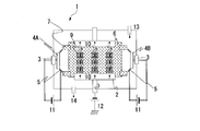
- film formation can be performed using the arc ion plating apparatus 1 whose outline is shown in FIGS. 1A and 1B.
- the space in front of the target is raised by providing a cylindrical heater 7 in front of the targets 4A and 4B, thereby generating from the targets 4A and 4B.
- the particles to be solidified in the atmosphere can be prevented, and when the particles adhere to the tool base 9 at a high temperature, the particles are deformed along the shape of the surface of the base by an impact at the time of attachment.
- the particles are deformed along the shape of the surface of the substrate with a smooth surface, and when viewed from the longitudinal section of the film (cross section perpendicular to the surface of the substrate), the particles have a flat shape along the surface of the substrate.
- the angle between the straight line forming the major axis of the cross section and the surface of the tool base is controlled to 45 degrees or less.
- Particles with an Al content of 50 atomic% or less are dispersed and distributed in the hard coating layer, and further, the particles have a flat shape with a large aspect ratio along the substrate surface, so that the resistance during cutting is reduced and the particles fall off. In addition, even if it falls off, damage in the layer thickness direction is reduced.
- the cylindrical heater 7 is disposed so that the thickness direction thereof is perpendicular to the corresponding usage surfaces of the targets 4A and 4B. And the cylindrical heater 7 is arrange
- the distance between the rear end of the cylindrical heater 7 (the side facing the corresponding target and close to the corresponding target) and the use surface of the corresponding target is set within 50 mm, for example.
- the distance between the front end of the cylindrical heater 7 (orienting in the same direction as the corresponding target and the side far from the corresponding target) and the use surface of the corresponding target is, for example, the distance from the target to the base (multiple arranged on the turntable)
- the distance to the closest base body) is set to 2/3 length. Further, damage to the coating film due to radiant heat from the cylindrical heater 7 can be prevented by providing a cooling mechanism in the tool base jig 8.
- a hard film having a characteristic feature of the surface-coated cutting tool which is one embodiment of the present invention is formed.
- composition of the particles in the (Al, Cr, Si) (C, N) layer or (Al, Cr, Si) N layer, the cross-sectional major axis, the aspect ratio of the longitudinal cross-sectional shape, and the straight line that forms the cross-sectional major axis are the surface of the substrate.
- the size of the straight line forming the major axis of the cross section of the particles having an angle of 45 degrees or less and the area A surrounded by the outer peripheral part of the particle on the hard coating surface side, and the area B surrounded by the outer peripheral part of the particle on the base side Has found that it can be controlled by adjusting the temperature inside the PVD apparatus, the arc current of the target, the total gas partial pressure of nitrogen and methane, and the like. Based on the above findings, the present invention has been completed. In addition, this invention is not limited to the said manufacturing method.
- This invention is made
- a hard coating layer comprising a composite nitride layer or a composite carbonitride layer of 5-8.0 ⁇ m Al, Cr and Si;
- the hard coating layer comprises a non-metallic component consisting of one or more selected from C and N of less than 10 atomic% and a metallic component that is one or more elements selected from Cr, Al, and Si. Containing a plurality of particles,
- C Among the plurality of particles, the Al content is 50 atomic% or less, the major axis in a cross section perpendicular to the surface of the tool base is less than 0.5 ⁇ m, and the aspect ratio is 2.
- the surface-coated cutting tool is characterized in that the flat particles that are 0 or more occupy 90% or more of the plurality of particles in the cross section in the number ratio.
- a coated tool which is an embodiment of the present invention is a surface coating in which a hard coating is formed on a surface of a tool substrate made of a tungsten carbide base cemented carbide by physical vapor deposition.
- a cutting tool wherein (a) the hard film is formed of one or more layers, and at least one of the layers is an average composition formula: (Al 1-xy Cr x Si y ) (C z N 1 -Z ) (where x, y and z are atomic ratios and satisfy 0.1 ⁇ x ⁇ 0.4, 0.01 ⁇ y ⁇ 0.2, 0 ⁇ z ⁇ 0.3)
- a hard coating layer composed of a composite nitride layer or a composite carbonitride layer of Al, Cr, and Si having an average layer thickness of 0.5 to 8.0 ⁇ m, and (b) the hard coating layer is less than 10 atomic% 1 or more selected from Cr, Al, Si and a non-metallic component consisting of one or more selected from C and N (C)
- the Al content is 50 atomic% or less, and the cross-sectional major axis perpendicular to the surface of the tool base is included.
- the flat particles having an aspect ratio of less than 0.5 ⁇ m and an aspect ratio of 2.0 or more occupy 90% or more in the cross section in the number ratio with respect to the total number of the plurality of particles. To do.
- the hard coating provided in the surface-coated cutting tool of the present invention exhibits excellent chipping resistance and welding resistance.
- the angle formed by the straight line forming the major axis of the cross section of each of the plurality of particles and the surface of the tool base is 45 degrees or less, and is surrounded by the straight line forming the major axis and the outer peripheral portion of the particle on the hard coating surface side.
- the particles satisfying A> B are 80% or more of the total number of the plurality of particles. Occupies the chipping resistance and welding resistance of the hard coating. As a result, for example, in milling processing of alloy tool steel or the like, excellent cutting performance is exhibited over a long period of use.
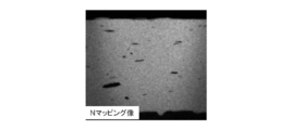
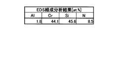
- an Si mapping image by EDS measured for the cross section of the (Al 0.63 Cr 0.27 Si 0.10 ) N layer of the coated tool 8 of the present invention is shown.
- it is an image obtained at the time of composition analysis of particles existing in the cross section of the (Al 0.63 Cr 0.27 Si 0.10 ) N layer of the coated tool 8 of the present invention. Indicates.
- grains shown to FIG. 3A is shown.
- Hard coating layer comprising (Al, Cr, Si) (C, N) layer or (Al, Cr, Si) N layer:
- a hard coating layer composed of an (Al, Cr, Si) (C, N) layer or an (Al, Cr, Si) N layer
- the constituent Al component improves high-temperature hardness and heat resistance
- Cr The component improves high temperature strength
- the Si component improves oxidation resistance.
- the coexistence of Al and Cr has the effect of improving high-temperature oxidation resistance.
- the Cr content ratio x in the total amount of Al, Cr and Si is less than 0.1.
- the Al content is relatively high, in the milling cutting of the work material having high weldability, it is not possible to ensure the welding resistance to the work material and chips, and the high temperature strength is also high. Since it decreases, welding and chipping are likely to occur.
- the Cr content ratio x in the total amount of Al, Cr, and Si exceeds 0.4, the melting point of the target material becomes high when the hard coating layer is formed by the PVD method, so that the secondary material is secondary.
- the spherical particles that are generated automatically have a high Cr concentration, and have a relatively high melting point as compared with particles having a Cr content ratio x in the total amount of Al, Cr, and Si of 0.4 or less.
- the Cr content ratio x in the total amount of Al, Cr, and Si is set to 0.1 to 0.4.
- the content ratio x is preferably 0.15 to 0.37, more preferably 0.2 to 0.3, but is not particularly limited by these.
- the ratio of the metal component to the non-metal component is not limited to the stoichiometric ratio of 1: 1, and the effect of the present invention can be obtained as long as the same crystal structure as in the case of 1: 1 is maintained.
- the Si content ratio y in the total amount of Al, Cr and Si is less than 0.01, not only the oxidation resistance improving effect is small, but also the Cr content ratio is relatively high, so the melting point of the particles is As described above, voids are formed under the particles contained in the (Al, Cr, Si) (C, N) layer or (Al, Cr, Si) N layer as described above, and the effect of improving chipping resistance is small. .
- the Si content ratio y in the total amount of Al, Cr and Si exceeds 0.2, the (Al, Cr, Si) (C, N) layer or the (Al, Cr, Si) N layer Therefore, the Si content ratio y in the total amount of Al, Cr and Si is set to 0.01 or more and 0.2 or less.
- the content ratio y is preferably 0.07 to 0.2, more preferably 0.1 to 0.15, but is not particularly limited by these.
- the content ratio z of C in the total amount of C and N exceeds 0.3, the hardness of the hard coating layer is excessively large, and thus chipping resistance is reduced in cutting. Therefore, the content ratio z of C in the total amount of C and N is set to 0.3 or less. Preferably, it is 0 to 0.2, but is not particularly limited by these.
- the average layer thickness of the (Al, Cr, Si) (C, N) layer or the (Al, Cr, Si) N layer is set to 0.5 ⁇ m or more and 8.0 ⁇ m or less.
- the average layer thickness of the (Al, Cr, Si) (C, N) layer or (Al, Cr, Si) N layer is 0.7 ⁇ m to 7.5 ⁇ m, but is not particularly limited by these.
- the plurality of particles contained in the hard coating layer of the present invention includes a non-metallic component (that is, at least one of C and N) of less than 10 atomic% and a metallic component (Cr, Al, Si) that is another component. 1 type or 2 types or more).
- the content of the nonmetallic component is preferably 0.5 atomic percent or more and less than 10 atomic percent.
- a trace amount of inevitable impurities may be mixed in the plurality of particles contained in the hard coating layer. However, this is not limited to the case where the inevitable impurities do not significantly affect the chipping resistance and / or welding resistance of the hard film including the hard coating layer.
- the content ratio of Al in the particles is mainly the nitrogen during film formation when the (Al, Cr, Si) (C, N) layer or (Al, Cr, Si) N layer is formed by the PVD method.
- the Al content in the particles can be reduced to 50 atomic% or less.
- the Al content in the plurality of particles (flat particles) is 50 atomic% or less.
- the content of Al in the particles is 0.5 to 50 atomic%, more preferably 0.5 to 20 atomic%, but is not particularly limited by these.
- Particles in the hard coating layer (Al, Cr, Si) (C, N) layer or (Al, Cr, Si) N layer contained in the hard coating of the coated tool of the present invention are perpendicular to the tool substrate surface.
- the cross-sectional major axis is 0.5 ⁇ m or more, particles having relatively small hardness are widely present in the layer, and the (Al, Cr, Si) (C, N) layer, or (Al, Cr, The hardness of the Si) N layer decreases, and as a result, sufficient wear resistance during cutting cannot be ensured.
- the aspect ratio of particles in the hard coating layer (Al, Cr, Si) (C, N) layer or (Al, Cr, Si) N layer contained in the hard film of the coated tool of the present invention is 2.
- the shape of the particles when the hard coating layer is formed by the PVD method becomes almost spherical, and voids are formed below the spherical particles, and these voids cause cracks during cutting. It becomes a starting point and reduces chipping resistance. Therefore, the cross-sectional major axis of the particles in the hard coating layer (Al, Cr, Si) (C, N) layer or (Al, Cr, Si) N layer included in the hard coating of the coated tool of the present invention is 0.00. It is less than 5 ⁇ m, and the aspect ratio of the particles is 2.0 or more.
- the Al content in all the particles is 50 atomic% or less
- the cross-sectional major axis is less than 0.5 ⁇ m
- the aspect ratio is not necessarily 2.0 or more.
- particles (flat particles) having a content of Al in the particles of 50 atomic% or less, a cross-sectional major axis of less than 0.5 ⁇ m, and an aspect ratio of 2.0 or more are particles. If the condition that the number ratio occupies 90% or more with respect to the total number is satisfied, the chipping resistance and welding resistance intended in the present invention can be obtained.
- the cross-sectional major axis of the particle contained in the hard coating layer of the surface-coated tool of the present invention is a straight line that can be drawn only within the particle when measured with respect to the cross-sectional shape of the particle in the cross-section of the film perpendicular to the substrate surface. Define the longest. That is, the straight line that temporarily goes out of the particle is not used for determining the cross-sectional major axis of the particle.
- the aspect ratio of the particles contained in the hard coating layer of the surface-coated tool of the present invention is the maximum value of the particle width perpendicular to the straight line forming the major axis of the above-mentioned cross section of the film perpendicular to the substrate surface.
- the minor axis it means the value of the major axis of the section / the minor axis of the section.
- the content of Al in all particles contained in the hard coating layer is 50 atomic% or less, the cross-sectional major axis is less than 0.5 ⁇ m, and the aspect ratio is 2.0.
- the angle between the straight line forming the major axis of the particle and the surface of the tool base is 45 degrees or less, and the straight line forming the major axis is surrounded by the outer peripheral portion of the particle on the hard coating surface side.
- the angle formed by the straight line forming the major axis of the particle and the surface of the tool base exceeds 45 degrees, or if A ⁇ B, the depth of the formed recess becomes relatively deep, and the shear direction by cutting Stress concentrates on the ridges of the recesses and becomes the starting point of cracks that propagate into the hard coating, and chipping is likely to occur.
- the angle formed by the straight line forming the major axis of the particle and the surface of the tool base is 45 degrees or less and A> B, the depth of the formed recess is relatively small. This is because concentration is difficult to occur and chipping can be suppressed.
- the angle formed by the straight line forming the major axis of the particle (flat particle) and the surface of the tool substrate is 45 degrees or less, and the straight line forming the major axis is surrounded by the outer peripheral portion of the particle on the hard coating surface side.
- the area is A and the area surrounded by the straight line and the outer periphery of the particle on the tool base side is B, it is desirable that the particles satisfying A> B occupy 80% or more of the total number of particles. As a result, chipping resistance and welding resistance are further improved and excellent cutting performance is exhibited.
- the composition of the hard coating layer and the particles contained in the hard coating layer can be determined by using a transmission electron microscope-energy dispersive X-ray spectroscopy (TEM-EDS) and observing the structure of the hard coating layer cross section perpendicular to the tool substrate surface. It can be obtained by performing a composition analysis. The observation range in this case is 20 ⁇ m in the direction parallel to the tool base surface. Then, by performing elemental mapping with a spatial resolution of 0.01 ⁇ m or less on the cross section of the hard coating layer, for example, a coated (Al, Cr, Si) (C, N) layer or (Al, Cr, Si) N It can be confirmed that the composition of the layer is within the specified range. At the same time, the composition of the particles can be analyzed by point analysis at the film cross section.
- TEM-EDS transmission electron microscope-energy dispersive X-ray spectroscopy
- the number ratio of particles having an Al content of 50 atomic% or less, a cross-sectional major axis of less than 0.5 ⁇ m, and an aspect ratio of 2.0 or more can be obtained as follows. About the coated tool used as a measuring object, a hard coating layer cross section is analyzed similarly to the above-mentioned analysis. First, the total number of particles existing within the observation range (5 ⁇ m ⁇ 5 ⁇ m) is counted by an N mapping image using TEM-EDS. Next, 90 atomic% or more of the constituent elements constituting the particle in the previous particle is an element selected from one or more of Cr, Al, and Si, and the Al content is 50 atomic% or less.
- the number of particles having a cross-sectional major axis of less than 0.5 ⁇ m and an aspect ratio of 2.0 or more is counted. Based on the results of counting the number of particles, particles having an Al content of 50 atomic% or less, a cross-sectional major axis of less than 0.5 ⁇ m, and an aspect ratio of 2.0 or more with respect to the previous particles The number ratio of (flat particles) is calculated.
- the number of the particles per area is preferably 1 / ⁇ m 2 to 5 / ⁇ m 2 .
- the angle formed by the straight line forming the cross-sectional major axis of each metal particle and the tool base surface is determined.
- the cross-sectional major axis of each particle is formed.
- the area A surrounded by the straight line and the particle outer peripheral part on the hard coating surface side and the area B surrounded by the straight line and the particle outer peripheral part on the tool base side are obtained, and A and B are compared, and A> B.
- the number ratio of particles is calculated.
- the method for calculating the area A and the area B is as follows.
- a TEM-EDS mapping image obtained by photographing each particle is used. By using the mapping image obtained by analyzing the amount of nitrogen, the boundary between the particles and the hard coating layer can be distinguished.
- the outer periphery of the particle is selected, and the enclosed area can be calculated using image analysis software (for example, Adobe photoshop). Let A be the calculated area. Further, the cross-sectional major axis of the particle and the outer peripheral part of the particle on the tool base side are selected, and the enclosed area is calculated using image analysis software, and this is defined as area B. This method is performed for each particle, and the number ratio of particles with A> B is calculated.
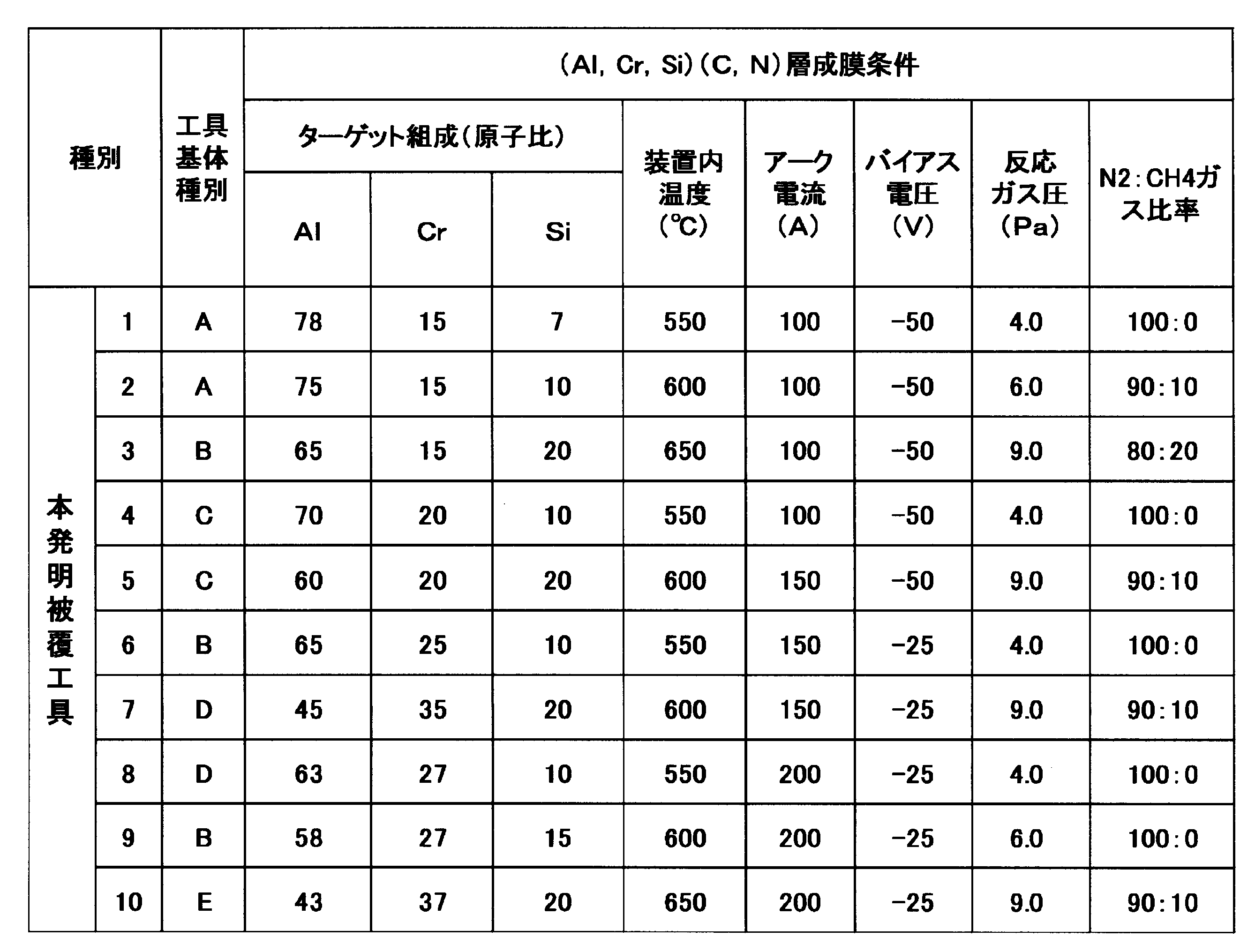
- these tool bases A to E were loaded into the arc ion plating apparatus shown in FIGS. 1A and 1B, and Ar bombardment was performed under the following conditions.
- the inside of the apparatus is evacuated and kept at a vacuum of 0.1 Pa or less, the inside of the apparatus is heated to 500 ° C. with a heater, and then the atmosphere of Ar gas pressure: 0.5 to 1.0 Pa is set.
- the bombardment treatment for 1 minute was repeated three times under the condition of current of 50 to 60 A to remove contaminants such as organic substances inevitably adhering to the tool substrate surface.
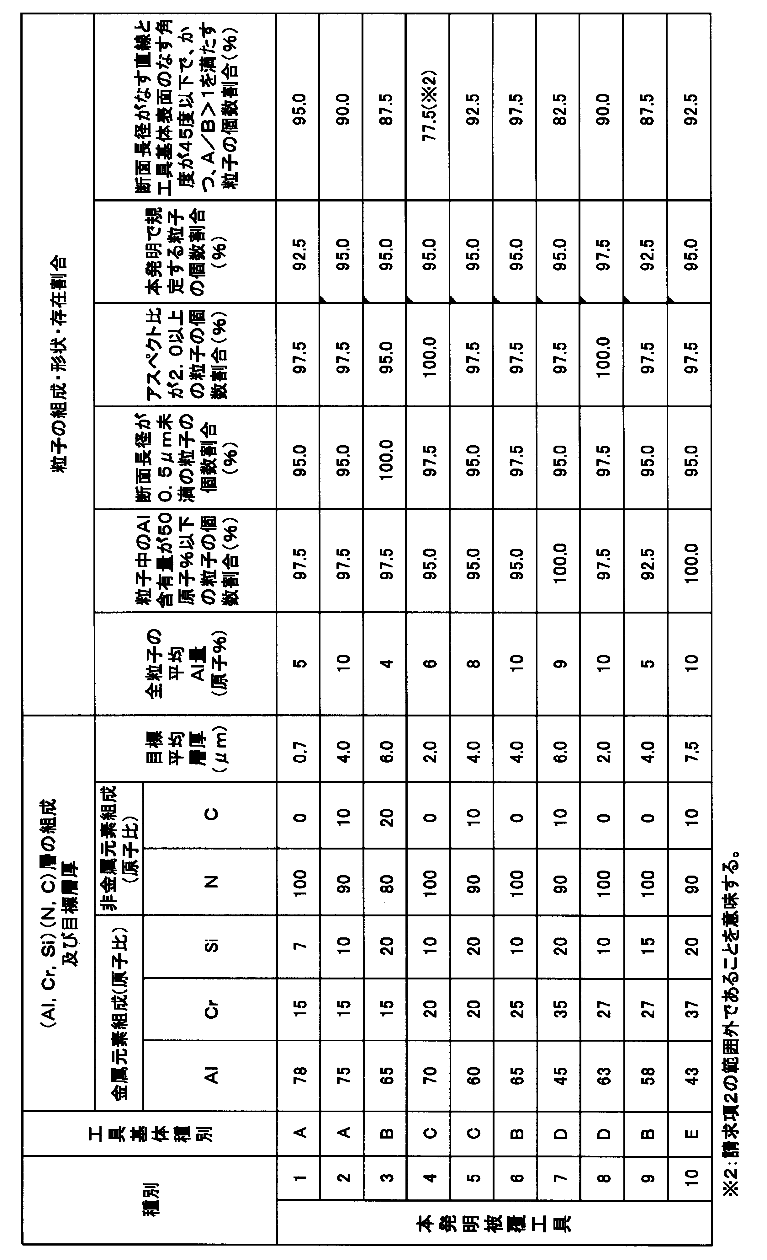
- the coated tools 1 to 10 of the present invention were prepared by vapor deposition.
- the temperature in the apparatus was increased from the conventional temperature (500 ° C.) because the time until the particle temperature fell below the melting point after the scattered particles adhered to the hard coating layer was lengthened. This is to facilitate formation of particles having an aspect ratio of 2.0 or more.
- the total gas partial pressure of nitrogen and methane was set in the range of 4 to 10 Pa because when the total gas partial pressure of nitrogen and methane was less than 4 Pa, the moving speed of the arc spot was relatively slow and the cross-sectional major axis was 0.
- the particles generated from the target can be prevented from solidifying in the atmosphere, and the particles deform along the shape of the tool base when adhering to the tool base. Damage to the film due to radiant heat from the cylindrical heater can be prevented by providing a cooling mechanism in the tool base jig.
- the cylindrical heater that heats the space in front of the target extends in the direction of the substrate when viewed from the target, and the length of the heater is about 2/3 to 3/4 of the distance between the target and the tool substrate. desirable. If it is too long, the coating will be damaged by radiant heat, while if it is too short, the high-temperature space existing on the front surface of the target will be narrowed, so that the particles will solidify before adhering to the tool base.
- the installation position is preferably within 50 mm from the target surface, and for example, it may be installed on the front surface of the anode electrode.
- a tool base cooling mechanism for example, there is a method of cooling by flowing cooling water through a tool base jig.
- the structure observation and composition of the hard coating layer cross section perpendicular to the tool base surface Analysis was performed using transmission electron microscope-energy dispersive X-ray spectroscopy (TEM-EDS).
- the observation range in each coated tool of the present invention is 20 ⁇ m in the direction parallel to the tool base surface.
- Element mapping with a spatial resolution of 0.01 ⁇ m or less is performed on the cross section of the hard coating layer, and the composition of the coated (Al, Cr, Si) (C, N) layer or (Al, Cr, Si) N layer is specified.
- the composition of the particles was analyzed by point analysis at the cross section of the film.
- the maximum diameter in the cross section of the particle is the long axis of the cross section
- the maximum value of the particle width perpendicular to the straight line forming the long axis of the cross section is the short axis of the cross section of the particle
- the total number of particles existing within the observation range of each coated tool of the present invention and 90 atomic% or more of the constituent elements constituting the particles are elements selected from one or more of Cr, Al, and Si And by counting the number of particles having an Al content of 50 atomic% or less, a cross-sectional major axis of less than 0.5 ⁇ m, and an aspect ratio of 2.0 or more, Al The number ratio of particles having a content of 50 atomic% or less, a cross-sectional major axis of less than 0.5 ⁇ m, and an aspect ratio of 2.0 or more was calculated.
- the angle formed by the straight line forming the cross-sectional major axis of each metal particle and the tool base surface is obtained, and for the particles having the angle of 45 degrees or less, the cross-sectional major axis of each particle
- the area A surrounded by the outer periphery of the particle on the surface side of the hard coating and the surface of the hard coating and the area B surrounded by the outer periphery of the particle on the side of the tool base are obtained, A and B are compared, and A> B
- the number ratio of the particles is calculated.
- the method for calculating the area A and the area B is as follows. A TEM-EDS mapping image obtained by photographing each particle is used.
- the boundary between the particles and the hard coating layer can be distinguished.
- the outer periphery of the particle is selected, and the enclosed area can be calculated using image analysis software (for example, Adobe Photoshop). Let A be the calculated area. Further, the cross-sectional major axis of the particle and the outer peripheral part of the particle on the tool base side are selected, and the enclosed area is calculated using image analysis software, and this is defined as area B. This method was performed on each particle, and the number ratio of particles with A> B was calculated. Table 3 shows these measured values and calculated values.
- 2A to 2E show, as an example, TEM-EDS mapping images measured for the cross section of the (Al 0.63 Cr 0.27 Si 0.10 ) N layer of the coated tool 8 of the present invention.
- 3A and 3B also show the composition analysis results measured for particles present in the cross section of the (Al 0.63 Cr 0.27 Si 0.10 ) N layer of the coated tool 8 of the present invention.
- Comparative coating tools 1 to 10 were prepared by vapor-depositing (Al, Cr, Si) (C, N) layers or (Al, Cr, Si) N layers having a predetermined layer thickness in which are distributed.
- the cross section of the (Al, Cr, Si) (C, N) layer or (Al, Cr, Si) N layer of the comparative coated tools 1 to 10 was also observed by TEM-EDS, and point analysis was performed on the film cross section.
- the composition of the particles was analyzed, and among the particles, particles having an Al content of 50 atomic% or less, a cross-sectional major axis of less than 0.5 ⁇ m, and an aspect ratio of 2.0 or more were included in the total number of particles.
- the angle formed by the straight line forming the cross-sectional major axis of each particle and the surface of the tool base is determined.
- the area A surrounded by the straight line forming the major axis of each particle and the outer periphery of the particle on the hard coating surface side, and the area surrounded by the outer periphery of the particle on the tool base side are obtained as B. Compare the target, A> B Of it was calculated number proportion to the total particles present in the measurement range. Table 5 shows these values.
- the thicknesses of the hard coatings of the inventive coated tools 1 to 10 and the comparative coated tools 1 to 10 were measured using a scanning electron microscope (SEM), the target layers shown in Tables 3 and 5 were all used. The average layer thickness was substantially the same as the thickness.
- the coated tools 1 to 10 of the present invention are in the (Al, Cr, Si) (C, N) layer or (Al, Cr, Si) N layer of the hard coating,
- the cross-sectional major axis is less than 0.5 ⁇ m and the aspect ratio is 2.0 or more, the ratio of the number of particles to the total number of particles is 90% or more. In addition to showing welding resistance, it showed excellent wear resistance.
- the angle formed by the straight line forming the cross-sectional major axis of the particle and the tool base surface is 45 degrees or less, and the straight line forming the major axis and the hard
- the area surrounded by the outer peripheral part of the particle on the surface side of the film is A
- the area surrounded by the outer peripheral part of the straight line and the particle on the tool base side is B
- the number of particles with A> B in the total number of particles Since the ratio was 80% or more, the chipping and welding resistance were further improved in the milling process, and as a result, the wear resistance was improved over a long period of time.
- the comparative coated tools 1 to 6 and 8 have particles formed in the hard coating, the Al content in the particles is 50 atomic% or less and the cross-sectional major axis is less than 0.5 ⁇ m.
- the ratio of the number of particles having an aspect ratio of 2.0 or more is outside the range specified in the present invention, it is clear that in milling processing, chipping, welding, etc., lead to a short life. is there.
- the angle formed by the straight line forming the cross-sectional major axis of the particle and the tool base surface is 45 degrees or less, and the straight line forming the major axis and the hard coating surface side
- the straight line forming the major axis and the hard coating surface side In the milling process, chipping, welding, etc., because the area A surrounded by the outer periphery of the particles and the area B surrounded by the straight line forming the major axis and the area B surrounded by the outer periphery of the particles on the tool base side do not satisfy the relationship of A> B. It is clear that the lifetime is reached in a shorter time due to the occurrence of.
- the comparative coated tools 7, 9, and 10 have particles formed in the hard coating layer, the composition or layer thickness of the hard coating layer is out of the range defined in the present invention. It is clear that the occurrence of a short life span.
- the coated tool of the present invention exhibits excellent chipping resistance and welding resistance in, for example, high-speed cutting of work materials such as carbon steel and alloy tool steel, thereby extending the service life. Needless to say, it is of course possible to use in cutting of other work materials and cutting under other conditions.
- the hard film which consists of one layer demonstrated in the said Example even if it is a case where a hard film consists of two or more layers, if the at least 1 layer is a film as described in the said Example, the same effect is obtained. It is what you play.
Landscapes
- Chemical & Material Sciences (AREA)
- Engineering & Computer Science (AREA)
- Mechanical Engineering (AREA)
- Chemical Kinetics & Catalysis (AREA)
- Materials Engineering (AREA)
- Metallurgy (AREA)
- Organic Chemistry (AREA)
- Cutting Tools, Boring Holders, And Turrets (AREA)
Abstract
Description
本願は、2015年1月22日に日本に出願された特願2015-010351号、および2016年1月20日に日本に出願された特願2016-8494号に基づき優先権を主張し、その内容をここに援用する。
即ち、特許文献1に示される表面被覆切削工具においては、硬質被覆層中に含有される粒子を構成する元素の90原子%以上が金属元素であり、しかも、構成元素の50原子%以上Alが含有されているため、粒子組成がAlリッチであって融点が低く、高温強度が保てず耐溶着性が悪くなるという問題がある。
また、特許文献2に示される表面被覆切削工具においては、硬質被覆層中に存在するドロップレットの下部には空隙が形成されており、その空隙が存在することで、外力が加わった際の硬質被覆層の強度が弱く、例えば、切削加工時に空隙がクラックの起点となり、チッピングが発生しやすくなるという問題がある。
さらに、特許文献3に示される表面被覆切削工具は、高負荷が作用する切削条件では、硬質被覆層の表面から突出する複数のマクロ粒子が脱落し、これがクラック発生の起点となるため満足できる耐チッピング性を発揮し得ないという問題があった。
この硬質被覆層は、硬質皮膜に含まれる層であり、AlとCrとSiの複合炭窒化物層(以下、「(Al、Cr、Si)(C、N)層」で示す)、または複合窒化物層(以下、「(Al、Cr、Si)N層」で示す)からなり、平均層厚は、0.5~8.0μmである。この硬質被覆層には、複数の粒子が含まれている。そして、これら複数の粒子のうち、構成元素の90原子%以上がCr、Al、Siのうち1種もしくは2種以上より選択された元素であり(10原子%未満がCおよびNから選ばれる1種以上である非金属元素)、構成元素の50原子%以下がAlであり、工具基体表面に垂直な縦方向断面における長径が0.5μm未満であり、縦断面形状のアスペクト比が2.0以上である粒子(以下、「偏平粒子」と称する)の、粒子全個数に対する個数割合は90%以上を占める。
このような粒子(偏平粒子)を含有する(Al、Cr、Si)(C、N)層、または(Al、Cr、Si)N層はすぐれた耐チッピング性、耐溶着性を示すようになる。その結果として、この硬質被覆層を含む硬質皮膜が被覆形成された表面被覆切削工具は、長期の使用にわたってすぐれた切削性能を発揮する。
さらに、前記偏平粒子の各粒子について、その断面長径をなす直線が基体表面となす傾斜角度を測定した場合、傾斜角度が45度以下であって、かつ、長径をなす直線と硬質皮膜表面側の粒子外周部で囲まれた面積をA、その直線と基体側の粒子外周部で囲まれた面積をBとした場合、A>Bである粒子が、粒子全個数に対して個数割合で80%以上を占めることがより好ましい。このような粒子を含有する(Al、Cr、Si)(C、N)層、または(Al、Cr、Si)N層は、より一段とすぐれた耐チッピング性、耐溶着性を示し、長期の使用にわたってより一段とすぐれた切削性能を発揮する。
例えば、本願発明では、図1Aおよび図1Bにその概略を示すアークイオンプレーティング装置1を用いて成膜を行うことができる。この場合、炉全体の雰囲気温度を制御するヒーター6に加え、好ましくは、ターゲット4A、4Bの前面に筒状ヒーター7を設けることでターゲット前面の空間を高温にし、これによりターゲット4A、4Bから発生する粒子が雰囲気中で凝固することを防ぐことができ、高温のまま工具基体9へ付着させることで、粒子は付着時の衝撃によって基体表面の形状に沿って変形する。そのため、粒子は、表面平滑な基体表面の形状に沿って変形し、皮膜の縦断面(基体表面に対して垂直な断面)からみた場合、基体表面に沿った扁平形状となり、粒子の断面形状の断面長径をなす直線と工具基体表面となす角度は45度以下に制御される。Al含有量が50原子%以下の粒子を硬質被覆層内に分散分布させ、さらに、粒子を基体表面に沿ったアスペクト比の大きい扁平形状とすることで切削時の抵抗が小さくなり、粒子は脱落しにくく、また脱落した場合でも層厚方向への損傷が小さくなる。その結果、耐チッピング性、耐溶着性にすぐれた硬質被覆層を提供できる。
筒状ヒータ7は、その厚み方向が対応するターゲット4A、4Bの使用面に垂直になるように配置される。そして、筒状ヒータ7は、ターゲット4A、4Bの使用面の中心が、筒状ヒーター7の中心軸と、重なるようにターゲット4A、4Bの前面に筒状ヒーター7を配置される。
筒状ヒータ7の後端(対応するターゲット対向し、対応するターゲットに近い側)と、対応するターゲットの使用面との距離は、例えば50mm以内に設定される。筒状ヒータ7の前端(対応するターゲットと同じ方向を向き、対応するターゲットから遠い側)と、対応するターゲットの使用面との距離は、例えばターゲットから基体距離(回転テーブル上に配された複数の基体のうち、最接近した基体までの距離)の2/3の長さに設定される。
また、筒状ヒーター7からの輻射熱による皮膜へのダメージは工具基体治具8に冷却機構を設けることで防ぐことができる。このような機構を有した成膜装置で成膜することで、本願発明の一態様である表面被覆切削工具が有する特徴のある硬質皮膜が形成される。
以上のような知見に基づき、本願発明を完成するに至った。なお、本願発明は上記製法に限定されるものではない。
(1)炭化タングステン基超硬合金からなる工具基体の表面に、硬質皮膜が形成されている表面被覆切削工具において、
(a)前記硬質皮膜は1または2以上の層から形成され、その少なくとも1層は、平均組成式:(Al1-x-yCrxSiy)(CzN1-z)(但し、x、y、zはいずれも原子比であって、0.1≦x≦0.4、0.01≦y≦0.2、0≦z≦0.3)を満足する平均層厚0.5~8.0μmのAlとCrとSiの複合窒化物層または複合炭窒化物層からなる硬質被覆層であり、
(b)前記硬質被覆層は、10原子%未満のCおよびNから選ばれる1種以上からなる非金属成分と、Cr、Al、Siから選ばれる1種以上の元素である金属成分とからなる複数の粒子を含み、
(c)前記複数の粒子のうち、Al含有量は50原子%以下であり、前記工具基体の表面に対して垂直な断面における長径が0.5μm未満であって、さらに、アスペクト比が2.0以上である偏平粒子は、前記複数の粒子の全個数に対して、個数割合で90%以上を前記断面中で占めることを特徴とする表面被覆切削工具。
(2)前記硬質皮膜の前記工具基体の表面に対して垂直な断面で、前記硬質被覆層に含有される前記偏平粒子を観察したときに、前記偏平粒子のそれぞれにおいて、前記長径をなす直線が工具基材表面となす角度は45度以下であり、かつ、前記直線と硬質皮膜表面側の粒子外周部とで囲まれた面積をA、前記直線と工具基体側の粒子外周部とで囲まれた面積をBとした場合、A>Bである粒子が、前記偏平粒子の全個数に対して個数割合で80%以上を占めることを特徴とする前記(1)記載の表面被覆切削工具。
(3)前記硬質被覆層の平均層厚が、0.7~7.5μmである前記(1)または(2)記載の表面被覆切削工具。
(4)前記硬質被覆層が、前記硬質皮膜の最外層である前記(1)乃至(3)のいずれかに記載の表面被覆切削工具。
(5)前記非金属成分の含有量が、0.5原子%以上10原子%未満である前記(1)記載の表面被覆切削工具。
(6)前記金属成分のAl含有量が、0.5原子%以上20原子%以下である前記(1)記載の表面被覆切削工具。
(7)前記断面における、前記複数の粒子の面積当たりの個数は、1個/μm2~5個/μm2である前記(1)記載の表面被覆切削工具。
さらに、前記硬質皮膜の前記工具基体の表面に対して垂直な断面で、前記AlとCrとSiの複合窒化物層または複合炭窒化物層に含有される前記複数の粒子を観察したときに、前記複数の粒子のそれぞれの前記断面の長径をなす直線が工具基材表面となす角度は45度以下であり、かつ、前記長径をなす直線と硬質皮膜表面側の粒子外周部とで囲まれた面積をA、その直線と工具基体側の粒子外周部とで囲まれた面積をBとした場合、A>Bである粒子が、前記複数の粒子の全個数に対して個数割合で80%以上を占めることにより、硬質皮膜が一段とすぐれた耐チッピング性、耐溶着性を示す。その結果、例えば、合金工具鋼等のミーリング加工において、長期の使用にわたってすぐれた切削性能を発揮する。
(Al、Cr、Si)(C、N)層、または(Al、Cr、Si)N層からなる硬質被覆層においては、その構成成分であるAl成分が高温硬さと耐熱性を向上させ、Cr成分が高温強度を向上させ、また、Si成分が耐酸化性を向上させる。さらに、AlとCrとが共存することによって高温耐酸化性を向上させる作用がある。
しかし、(Al、Cr、Si)(C、N)層、または(Al、Cr、Si)N層において、AlとCrとSiとの合量に占めるCrの含有割合xが0.1未満であると、相対的にAl含有量が高くなるため、溶着性の高い被削材のミーリング切削加工において、被削材および切粉に対する耐溶着性を確保することができず、また、高温強度も低下するため、溶着、チッピングを発生しやすくなる。一方、AlとCrとSiとの合量に占めるCrの含有割合xが0.4を越えると、硬質被覆層をPVD法で成膜する際に、ターゲット材の融点が高くなり、そのため副次的に生成される球状の粒子は高Cr濃度となり、AlとCrとSiとの合量に占めるCrの含有割合xが0.4以下である粒子と比べて融点が相対的に高くなる。そのため、ターゲットから発生した粒子が皮膜に付着した後、固着するまで奪熱する熱量が少ないため、球状の形状を保ったまま固着する。その上に皮膜が堆積することによって、粒子下部に空隙が残る。この空隙が存在することで、切削加工時に空隙が起点となってクラックが発生し、チッピングが発生しやすくなる。
したがって、AlとCrとSiとの合量に占めるCrの含有割合xは、0.1以上0.4以下とする。好ましくは、含有割合xは0.15~0.37であり、より好ましくは、0.2~0.3であるが、これらにより特に限定されない。
なお金属成分と非金属成分の比は化学量論比である1:1に限定されず、1:1の場合と同一の結晶構造が維持されていれば本願発明の効果を得ることができる。
さらに、CとNとの合量に占めるCの含有割合zが0.3を超えると、硬質被覆層の硬さが過大に大きいため、切削加工において耐チッピング性が低下する。そのため、CとNとの合量に占めるCの含有割合zは、0.3以下とする。好ましくは、0~0.2であるが、これらにより特に限定されない。
したがって、(Al、Cr、Si)(C、N)層、または(Al、Cr、Si)N層の平均層厚は、0.5μm以上8.0μm以下とした。好ましくは、(Al、Cr、Si)(C、N)層、または(Al、Cr、Si)N層の平均層厚は0.7μm~7.5μmであるが、これらにより特に限定されない。
本願発明の硬質被覆層に含まれる複数の粒子とは、10原子%未満の非金属成分(すなわち、C、Nの少なくとも1種以上)と、その他の成分である金属成分(Cr、Al、Siのうち1種もしくは2種以上)と、からなる塊を意味する。
前記非金属成分の含有量は、0.5原子%以上10原子%未満が好ましい。また、硬質被覆層に含まれる複数の粒子には、前記非金属成分および金属成分に加えて微量の不可避不純物が混入されてもよい。ただし、この不可避不純物の混入が、この硬質被覆層を含む硬質膜の耐チッピング性及び/又は耐溶着性に顕著に影響を及ぼさない場合に限る。
粒子中におけるAlの含有割合は、PVD法により(Al、Cr、Si)(C、N)層、または(Al、Cr、Si)N層を成膜する際の、主として成膜時の窒素及びメタンの合計ガス分圧を4~10Paの範囲内に制御することにより、粒子におけるAlの含有量を50原子%以下とすることができる。
粒子におけるAlの含有量が50原子%を超えると、(Al、Cr、Si)(C、N)層、または(Al、Cr、Si)N層よりも融点が低い粒子が層中に存在することになり、その部位が原因で高温強度を保てなくなるため溶着を発生しやすくなる。
したがって、複数の粒子(偏平粒子)におけるAlの含有量は50原子%以下とする。好ましくは、粒子におけるAlの含有量は0.5~50原子%であり、より好ましくは、0.5~20原子%であるが、これらにより特に限定されない。
また、本発明の被覆工具の有する硬質皮膜に含まれる硬質被覆層(Al、Cr、Si)(C、N)層、または(Al、Cr、Si)N層中における粒子のアスペクト比が2.0未満になると、硬質被覆層をPVD法で成膜した際の粒子の形状がほぼ球状となるため、該球状の粒子下部に空隙が形成されてしまい、この空隙が切削加工時のクラック発生の起点となり、耐チッピング性を低下させる。
したがって、本発明の被覆工具の有する硬質皮膜に含まれる硬質被覆層(Al、Cr、Si)(C、N)層、または(Al、Cr、Si)N層中における粒子の断面長径は0.5μm未満、また、粒子のアスペクト比は2.0以上とする。
但し、全ての粒子中のAlの含有量が50原子%以下であり、かつ、その断面長径が0.5μm未満であり、さらに、アスペクト比が2.0以上である必要はなく、全体の粒子のうち、粒子中のAlの含有量が50原子%以下であり、かつ、断面長径が0.5μm未満であって、しかも、アスペクト比が2.0以上である粒子(偏平粒子)が、粒子全個数に対して個数割合で90%以上を占めるという条件を満たせば、本願発明で目的とする耐チッピング性、耐溶着性を得ることができる。
さらに、本願発明の表面被覆工具の硬質被覆層に含まれる粒子のアスペクト比とは、基体表面に垂直な皮膜断面において、上記断面長径をなす直線に直交する粒子幅の最大の値を粒子の断面短径とした場合に、断面長径/断面短径の値をいう。
即ち、切削加工時に硬質被覆層の摩耗が進行するにつれ、粒子(偏平粒子)が硬質被覆層表面に露出し、硬質被覆層と比べて粒子の硬さが小さいため、硬質被覆層と比べて粒子部で摩耗の進行が速い。そのため、硬質被覆層と比べ粒子部が深くえぐられるように摩耗が進行し、凹部が形成される。このとき、粒子の断面長径をなす直線が工具基体表面となす角度が45度を超える、あるいは、A≦Bであると、形成される凹部の深さが相対的に深くなり、切削によるせん断方向の応力が凹部の淵に集中し、硬質皮膜中に進展する亀裂の起点となり、チッピングが発生し易い。しかし、粒子の断面長径をなす直線が工具基体表面となす角度が45度以下、かつ、A>Bであれば、形成される凹部の深さは相対的に小さいため、切削時のせん断力の集中が生じにくく、チッピングの発生は抑えられるという理由による。
したがって、本願発明では、粒子(偏平粒子)の断面長径をなす直線が工具基材表面となす角度が45度以下、かつ、該長径をなす直線と硬質皮膜表面側の粒子外周部で囲まれた面積をA、その直線と工具基体側の粒子外周部で囲まれた面積をBとした場合、A>Bである粒子が、粒子全個数に対して個数割合で80%以上を占めることが望ましく、これによって、より一段と耐チッピング性、耐溶着性が向上し、すぐれた切削性能を発揮する。
まず、装置内を排気して0.1Pa以下の真空に保持しながら、ヒーターで装置内を500℃に加熱した後、Arガス圧力:0.5~1.0Paの雰囲気とすると共に、タングステンフィラメントに電流50~60Aの条件下で1分のボンバード処理を3回繰り返し、工具基体表面に不可避的に付着している有機物等の汚染物を除去した。
また、窒素及びメタンの合計ガス分圧を4~10Paの範囲内としたのは、窒素及びメタンの合計ガス分圧が4Pa未満では、アークスポットの移動速度が相対的に遅く、断面長径が0.5μm以上の粒子が発生しやすくなり、この粒子は、(Al、Cr、Si)(C、N)層、または(Al、Cr、Si)N層と比較して相対的に窒化の程度が少なく硬さが小さいため、硬質皮膜全体としての硬さが小さくなり切削加工時に耐摩耗性が低下する。一方、窒素及びメタンの合計ガス分圧が10Paを超えると、アークスポットの運動が不安定で成膜自体が困難になるとの理由による。
なお、装置内の温度を従来(500℃)よりも高くする際に、ターゲット前面に筒状ヒーターを設けることでターゲット前面の空間を高温にすることも有効である。これによりターゲットから発生する粒子が雰囲気中で凝固することを防ぐことができ、粒子は工具基体へ付着した際に工具基体の形状に沿って変形する。筒状ヒーターからの輻射熱による皮膜へのダメージは工具基体用治具に冷却機構を設けることで防ぐことができる。ターゲット前面の空間を加熱する筒状ヒーターはターゲットから見て基板方向に伸びており、長さはヒーターの先端がターゲット-工具基体間距離の2/3~3/4ほどの位置にあることが望ましい。長すぎると皮膜に輻射熱によるダメージが入り、一方で短すぎるとターゲット前面に存在する高温の空間が狭くなるため、工具基体付着前に粒子が凝固してしまう。ターゲット前面の空間を適切に加熱するためには、設置位置はターゲット表面から50mm以内の位置が望ましく、例えば、アノード電極の前面などに設置すると良い。工具基体の冷却機構は、例えば、工具基体用治具に冷却水を流して冷却する方法がある。
次に、粒子の断面における最大径を断面長径とし、該断面長径をなす直線に直交する粒子幅の最大の値を粒子の断面短径とし、各粒子について断面長径、断面短径を求めるとともに、断面長径、断面短径から各々の粒子のアスペクト比(=断面長径/断面短径)を求めた。
また、各本発明被覆工具の観察範囲内に存在する粒子の全個数と、粒子を構成する構成元素の90原子%以上はCr、Al、Siのうち1種もしくは2種以上より選択された元素であり、かつ、Al含有量が50原子%以下であり、かつ、断面長径が0.5μm未満であって、さらに、アスペクト比が2.0以上である粒子の個数をカウントすることにより、Al含有量が50原子%以下であり、かつ、断面長径が0.5μm未満であり、さらに、アスペクト比が2.0以上である粒子の個数割合を算出した。
さらに、観察範囲内に存在する全粒子について、それぞれの金属粒子の断面長径をなす直線が工具基材表面となす角度を求めるとともに、該角度が45度以下の粒子については、各粒子の断面長径をなす直線と硬質皮膜表面側の粒子外周部で囲まれた面積Aと、その直線と工具基体側の粒子外周部で囲まれた面積Bとを求め、AとBを比較し、A>Bである粒子の個数割合を算出する。なお、面積A及び面積Bを算出する方法は、以下の通りである。各粒子を撮影したTEM―EDSマッピング像を用いる。窒素量を分析したマッピング像を用いることで、粒子と硬質被覆層の境界を区別できる。粒子の外周部を選択し、囲まれた面積は、画像解析ソフト(例えば、Adobe Photoshopなど)を用いて算出できる。算出した面積をAとする。また、粒子の断面長径及び工具基体側の粒子外周部を選択し、囲まれた面積について画像解析ソフトを用いて算出し、これを面積Bとする。本方法を各粒子で行い、A>Bである粒子の個数割合を算出した。
表3に、これらの測定値、算出値をそれぞれ示す。
また、図3Aおよび図3Bに、同じく本発明被覆工具8の(Al0.63Cr0.27Si0.10)N層の断面に存在する粒子について測定した組成分析結果を示す。
表5に、これらの値をそれぞれ示す。


被削材:JIS・SKD61(HRC52)のブロック材
回転速度:17000/min.、
切削速度:300m/min.、
切り込み:ap 2.0mm、ae 0.3mm
送り速度(1刃当り):0.06mm/刃、
切削油剤:エアー、
切削長:300m、
表6に、前記切削試験の結果を示すとともに、チッピング、溶着発生の有無を示す。

また、本発明の被覆工具1~3、5~10は、前記粒子のうち、粒子の断面長径をなす直線が工具基材表面となす角度が45度以下、かつ、該長径をなす直線と硬質皮膜表面側の粒子外周部で囲まれた面積をA、その直線と工具基体側の粒子外周部で囲まれた面積をBとした場合、A>Bである粒子が、粒子全個数に占める個数割合で80%以上であることから、ミーリング加工においてより一段とすぐれた耐チッピング性、耐溶着性を示し、その結果、長期にわたってすぐれた耐摩耗性を示した。
また、比較被覆工具7、9、10は、硬質被覆層中に粒子は形成されるものの、硬質被覆層の組成、または、層厚が本願発明で規定する範囲から外れるため、ミーリング加工において、チッピングの発生により短時間で寿命にいたることが明らかである。
また前記実施例では1層からなる硬質皮膜にて説明したが、硬質皮膜が2以上の層から成る場合であっても、少なくとも1層が前記実施例に記載の皮膜であれば同様の効果を奏するものである。
2 回転テーブル
3 電磁コイル
4A カソード電極(AlCrSi合金)
4B カソード電極(ターゲット)(AlCrSi合金もしくは下部層成膜用ターゲット)
5 アノード電極
6 ヒーター
7 筒状ヒーター
8 工具基体用治具
9 基体
10 冷却水
11 アーク電源
12 バイアス電源
13 反応ガス
14 排ガス
15 粒子
16 測定箇所
W1 ターゲット表面から筒状ヒーター先端面までの距離(例えばターゲット-基板距離の2/3程度の長さ)
W2 ターゲット表面から筒状ヒーター後端面前の距離(例えば50mm以内)
Claims (8)
- 炭化タングステン基超硬合金からなる工具基体の表面に、硬質皮膜が形成されている表面被覆切削工具において、
(a)前記硬質皮膜は1または2以上の層から形成され、その少なくとも1層は、平均組成式:(Al1-x-yCrxSiy)(CzN1-z)(但し、x、y、zはいずれも原子比であって、0.1≦x≦0.4、0.01≦y≦0.2、0≦z≦0.3)を満足する平均層厚0.5~8.0μmのAlとCrとSiの複合窒化物層または複合炭窒化物層からなる硬質被覆層であり、
(b)前記硬質被覆層は、10原子%未満のCおよびNから選ばれる1種以上からなる非金属成分と、Cr、Al、Siから選ばれる1種以上の元素である金属成分とからなる複数の粒子を含み、
(c)前記複数の粒子のうち、Al含有量は50原子%以下であり、前記工具基体の表面に対して垂直な断面における長径が0.5μm未満であって、さらに、アスペクト比が2.0以上である偏平粒子は、前記複数の粒子の全個数に対して、個数割合で90%以上を前記断面中で占めることを特徴とする表面被覆切削工具。 - 前記硬質皮膜の前記工具基体の表面に対して垂直な断面で、前記硬質被覆層に含有される前記偏平粒子を観察したときに、前記偏平粒子のそれぞれにおいて、前記長径をなす直線が工具基材表面となす角度は45度以下であり、かつ、前記直線と硬質皮膜表面側の粒子外周部とで囲まれた面積をA、前記直線と工具基体側の粒子外周部とで囲まれた面積をBとした場合、A>Bである粒子が、前記偏平粒子の全個数に対して個数割合で80%以上を占めることを特徴とする請求項1記載の表面被覆切削工具。
- 前記硬質被覆層の平均層厚が、0.7~7.5μmである請求項1または2記載の表面被覆切削工具。
- 前記硬質被覆層が、前記硬質皮膜の最外層である請求項1または2記載の表面被覆切削工具。
- 前記硬質被覆層が、前記硬質皮膜の最外層である請求項3記載の表面被覆切削工具。
- 前記非金属成分の含有量が、0.5原子%以上10原子%未満である請求項1記載の表面被覆切削工具。
- 前記金属成分のAl含有量が、0.5原子%以上20原子%以下である請求項1記載の表面被覆切削工具。
- 前記断面における、前記複数の粒子の面積当たりの個数は、1個/μm2~5個/μm2である請求項1記載の表面被覆切削工具。
Priority Applications (4)
| Application Number | Priority Date | Filing Date | Title |
|---|---|---|---|
| KR1020177019832A KR20170103828A (ko) | 2015-01-22 | 2016-01-22 | 표면 피복 절삭 공구 |
| EP16740288.2A EP3248722A4 (en) | 2015-01-22 | 2016-01-22 | Cutting tool for surface coating |
| US15/545,182 US10569339B2 (en) | 2015-01-22 | 2016-01-22 | Surface-coated cutting tool |
| CN201680005874.3A CN107206513B (zh) | 2015-01-22 | 2016-01-22 | 表面包覆切削工具 |
Applications Claiming Priority (4)
| Application Number | Priority Date | Filing Date | Title |
|---|---|---|---|
| JP2015-010351 | 2015-01-22 | ||
| JP2015010351 | 2015-01-22 | ||
| JP2016-008494 | 2016-01-20 | ||
| JP2016008494A JP6593776B2 (ja) | 2015-01-22 | 2016-01-20 | 表面被覆切削工具 |
Publications (1)
| Publication Number | Publication Date |
|---|---|
| WO2016117681A1 true WO2016117681A1 (ja) | 2016-07-28 |
Family
ID=56417211
Family Applications (1)
| Application Number | Title | Priority Date | Filing Date |
|---|---|---|---|
| PCT/JP2016/051843 WO2016117681A1 (ja) | 2015-01-22 | 2016-01-22 | 表面被覆切削工具 |
Country Status (1)
| Country | Link |
|---|---|
| WO (1) | WO2016117681A1 (ja) |
Cited By (1)
| Publication number | Priority date | Publication date | Assignee | Title |
|---|---|---|---|---|
| US10751806B2 (en) | 2016-03-11 | 2020-08-25 | Mitsubishi Materials Corporation | Surface-coated cutting tool having excellent chipping resistance and wear resistance |
Citations (2)
| Publication number | Priority date | Publication date | Assignee | Title |
|---|---|---|---|---|
| JP2013046954A (ja) * | 2011-05-24 | 2013-03-07 | Mitsubishi Materials Corp | 耐欠損性と耐摩耗性にすぐれた表面被覆切削工具 |
| JP2014087861A (ja) * | 2012-10-29 | 2014-05-15 | Mitsubishi Materials Corp | 耐欠損性と耐摩耗性にすぐれた表面被覆切削工具 |
-
2016
- 2016-01-22 WO PCT/JP2016/051843 patent/WO2016117681A1/ja active Application Filing
Patent Citations (2)
| Publication number | Priority date | Publication date | Assignee | Title |
|---|---|---|---|---|
| JP2013046954A (ja) * | 2011-05-24 | 2013-03-07 | Mitsubishi Materials Corp | 耐欠損性と耐摩耗性にすぐれた表面被覆切削工具 |
| JP2014087861A (ja) * | 2012-10-29 | 2014-05-15 | Mitsubishi Materials Corp | 耐欠損性と耐摩耗性にすぐれた表面被覆切削工具 |
Non-Patent Citations (1)
| Title |
|---|
| See also references of EP3248722A4 * |
Cited By (1)
| Publication number | Priority date | Publication date | Assignee | Title |
|---|---|---|---|---|
| US10751806B2 (en) | 2016-03-11 | 2020-08-25 | Mitsubishi Materials Corporation | Surface-coated cutting tool having excellent chipping resistance and wear resistance |
Similar Documents
| Publication | Publication Date | Title |
|---|---|---|
| JP6634647B2 (ja) | 耐チッピング性、耐摩耗性にすぐれた表面被覆切削工具 | |
| JP4846519B2 (ja) | 窒化物含有ターゲット材 | |
| JP5962846B2 (ja) | 被覆切削工具 | |
| EP3130686B1 (en) | Cermet and cutting tool | |
| JP6421934B2 (ja) | 耐異常損傷性と耐摩耗性に優れた表面被覆切削工具 | |
| JP7068646B2 (ja) | 表面被覆切削工具 | |
| WO2018051939A1 (ja) | 表面被覆切削工具 | |
| JP5920577B2 (ja) | 耐欠損性と耐摩耗性にすぐれた表面被覆切削工具 | |
| JP6593776B2 (ja) | 表面被覆切削工具 | |
| WO2016084939A1 (ja) | 耐チッピング性、耐摩耗性にすぐれた表面被覆切削工具 | |
| JP5930187B2 (ja) | 耐欠損性と耐摩耗性にすぐれた表面被覆切削工具 | |
| JP6493800B2 (ja) | 高速切削加工ですぐれた耐摩耗性を発揮する表面被覆切削工具 | |
| JP7205709B2 (ja) | 表面被覆切削工具 | |
| WO2016117681A1 (ja) | 表面被覆切削工具 | |
| JP2017159424A (ja) | 耐チッピング性と耐摩耗性にすぐれた表面被覆切削工具 | |
| JP5991529B2 (ja) | 耐欠損性と耐摩耗性にすぐれた表面被覆切削工具 | |
| JP6796257B2 (ja) | 硬質被覆層がすぐれた耐チッピング性、耐剥離性を発揮する表面被覆切削工具 | |
| JP6399401B2 (ja) | 耐チッピング性、耐溶着性及び耐摩耗性にすぐれた表面被覆切削工具 | |
| JP7144747B2 (ja) | 表面被覆切削工具 | |
| JP2017159423A (ja) | 耐チッピング性と耐摩耗性にすぐれた表面被覆切削工具 | |
| JP2013082057A (ja) | 耐欠損性と耐摩耗性にすぐれた表面被覆切削工具 | |
| JP7217866B2 (ja) | 表面被覆切削工具 | |
| KR102278436B1 (ko) | 내치핑성과 내마모성이 우수한 표면 피복 절삭 공구 | |
| JP7054473B2 (ja) | 表面被覆切削工具 | |
| JP2018016875A (ja) | 複合部材およびこれからなる切削工具 |
Legal Events
| Date | Code | Title | Description |
|---|---|---|---|
| 121 | Ep: the epo has been informed by wipo that ep was designated in this application |
Ref document number: 16740288 Country of ref document: EP Kind code of ref document: A1 |
|
| ENP | Entry into the national phase |
Ref document number: 20177019832 Country of ref document: KR Kind code of ref document: A |
|
| WWE | Wipo information: entry into national phase |
Ref document number: 15545182 Country of ref document: US |
|
| REEP | Request for entry into the european phase |
Ref document number: 2016740288 Country of ref document: EP |
|
| NENP | Non-entry into the national phase |
Ref country code: DE |