WO2016117367A1 - 時間測定装置 - Google Patents
時間測定装置 Download PDFInfo
- Publication number
- WO2016117367A1 WO2016117367A1 PCT/JP2016/050335 JP2016050335W WO2016117367A1 WO 2016117367 A1 WO2016117367 A1 WO 2016117367A1 JP 2016050335 W JP2016050335 W JP 2016050335W WO 2016117367 A1 WO2016117367 A1 WO 2016117367A1
- Authority
- WO
- WIPO (PCT)
- Prior art keywords
- signal
- clock
- phase
- clock signal
- level
- Prior art date
- Legal status (The legal status is an assumption and is not a legal conclusion. Google has not performed a legal analysis and makes no representation as to the accuracy of the status listed.)
- Ceased
Links
Images








Classifications
-
- G—PHYSICS
- G04—HOROLOGY
- G04F—TIME-INTERVAL MEASURING
- G04F10/00—Apparatus for measuring unknown time intervals by electric means
- G04F10/06—Apparatus for measuring unknown time intervals by electric means by measuring phase
-
- H—ELECTRICITY
- H03—ELECTRONIC CIRCUITRY
- H03K—PULSE TECHNIQUE
- H03K21/00—Details of pulse counters or frequency dividers
- H03K21/02—Input circuits
- H03K21/026—Input circuits comprising logic circuits
-
- H—ELECTRICITY
- H03—ELECTRONIC CIRCUITRY
- H03K—PULSE TECHNIQUE
- H03K5/00—Manipulating of pulses not covered by one of the other main groups of this subclass
- H03K5/13—Arrangements having a single output and transforming input signals into pulses delivered at desired time intervals
- H03K5/135—Arrangements having a single output and transforming input signals into pulses delivered at desired time intervals by the use of time reference signals, e.g. clock signals
-
- G—PHYSICS
- G04—HOROLOGY
- G04F—TIME-INTERVAL MEASURING
- G04F10/00—Apparatus for measuring unknown time intervals by electric means
- G04F10/04—Apparatus for measuring unknown time intervals by electric means by counting pulses or half-cycles of an AC
Definitions
- the present invention relates to a time measuring device.
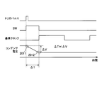
- FIG. 20 is a schematic configuration diagram of a conventional time measuring apparatus capable of obtaining a measurement resolution less than a clock period
- FIG. 21 is an operation explanatory diagram of the time measuring apparatus of FIG. 20 (see, for example, Patent Document 1). ).
- the capacitor C is charged to a constant voltage in advance.
- the switch SW is turned on to connect the capacitor C to the constant current circuit, and the discharge of the accumulated charge in the capacitor C is started.
- the discharge is stopped by turning off the switch SW at the timing when the reference clock is received after the trigger pulse (up edge timing of the reference clock).
- a voltage change ⁇ V between both poles of the capacitor C due to discharge is read by an AD converter.
- the voltage ⁇ V Since the integrated charge amount discharged using the constant current circuit is proportional to the discharge time, the voltage ⁇ V has a value corresponding to the time difference ⁇ T between the trigger pulse and the reference clock. Therefore, information about the time interval less than the clock period can be obtained from the voltage ⁇ V.
- an object of the present invention is to provide a time measuring device that contributes to improving the measurement accuracy of the time interval between two signals.
- a time measuring apparatus is a time measuring apparatus for measuring a time interval between input timings of a first target signal and a second target signal each having a pulse shape, and a clock signal having a predetermined clock frequency and clock cycle is measured.
- a period number detection unit that detects the time interval in units of the clock period, and receives at least one of the first and second target signals as a filter target signal and outputs a signal of the clock frequency from the filter target signal It has a bandpass filter for extracting components, and uses a phase detection unit for detecting a phase difference between the extracted signal and the clock signal, a detection result of the period number detection unit and a detection phase difference by the phase detection unit, And an arithmetic unit that obtains the time interval with a resolution smaller than the clock period.
- the pulsed filter target signal includes signal components of various frequencies including the clock frequency
- the phase difference between the extracted signal and the clock signal represents a time component smaller than the clock cycle in the time interval
- the detection result of the cycle number detection unit and the phase difference detected by the phase detection unit The time interval can be obtained with a resolution smaller than the clock cycle.
- the present invention can provide a time measuring device that contributes to improving the measurement accuracy of the time interval between two signals.
- FIG. 1 is a block diagram of a time measuring device (time interval measuring device) according to the first embodiment.
- the time measuring apparatus of FIG. 1 includes each part referred to by reference numerals 10, 20, 30, 40, 51 and 52.
- An arbitrary rectangular wave signal (including a digital signal such as a clock signal) handled by the time measuring device is a voltage signal and alternatively takes a low level or a high level signal level higher than the low level. .
- a rectangular wave signal including a digital signal such as a clock signal
- a transition from a low level to a high level of a signal level is expressed as an up edge, and the timing of the transition is expressed as an up edge timing.
- the time measurement device, start trigger signal trig_str and stop trigger signal trig_stp is is inputted, a clock signal clk having a predetermined clock frequency and the clock period T RF are input.
- Each of the start trigger signal trig_str and the stop trigger signal trig_stp is a pulse-shaped rectangular wave signal.
- a clock generator (not shown) for generating the clock signal clk may be included in the time measuring device.
- the stop trigger signal trig_stp is input to the time measuring device after the start trigger signal trig_str.
- the clock frequency of the clock signal clk is 5.7 GHz (gigahertz).
- the clock period T RF is about 175 picoseconds.
- the start trigger signal trig_str is input to the start side phase detection unit 10 via the signal distributor 51, and the stop trigger signal trig_stp is input to the stop side phase detection unit 20 via the signal distributor 52.
- the signal distributor 51 supplies the counter unit 30 with a signal in which the signal strength of the start trigger signal trig_str is reduced, that is, the start trigger signal trig_str ′ in which the signal strength is reduced.
- the signal distributor 52 supplies the counter unit 30 with a signal obtained by reducing the signal strength of the stop trigger signal trig_stp, that is, the stop trigger signal trig_stp ′ having a reduced signal strength.
- Signal distributors 51 and 52 are used for signal distribution.
- the signal-to-noise ratio can be improved by increasing the signal strength of the input signals (trig_str, trig_stp).
- the signal distributors 51 and 52 may be provided with attenuators for logic signals.
- the signal strength of the start trigger signal and the stop trigger signal may be reduced inside the counter unit 30 (in this case, the signal strength reduction function in the signal distributors 51 and 52 may be deleted).
- the start-side phase detection unit 10 detects the phase ⁇ str of the start trigger signal trig_str based on the clock signal clk (in other words, the phase ⁇ str of the clock signal clk at the timing when the start trigger signal trig_str is input to the time measurement device). And output.
- the stop-side phase detection unit 20 detects the phase ⁇ stp of the stop trigger signal trig_stp with reference to the clock signal clk (in other words, the phase ⁇ stp of the clock signal clk at the timing when the stop trigger signal trig_stp is input to the time measurement device). And output.
- the units of the phases ⁇ str and ⁇ stp are expressed in degrees. That is, each of the phases ⁇ str and ⁇ stp takes any value from 0 ° to 360 °.
- the phase of any clock signal including the clock signal clk takes any value from 0 ° to 360 °.
- the phase of the clock signal is 0 ° at the up-edge timing of the clock signal.
- the start trigger signal trig_str pulse width (interval signal trig_str becomes high level) (the same is true for stop trigger signal) is assumed to be three times the clock period T RF.
- the phase ⁇ stp is 0 °.
- the time measuring device can obtain the time interval T INT of the input timing of the start trigger signal trig_str and the stop trigger signal trig_stp to the time measuring device.
- Input timings of the start trigger signal trig_str and the stop trigger signal trig_stp to the time measuring device are timings t A and t B , respectively. That is, the time interval T INT represents the time difference between the timings t A and t B.
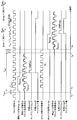
- the signal S N in FIG. 2 is an internal signal of the counter unit 30, and the value N is determined by the number of clocks in the signal S N.
- the time resolution in the counter unit 30 can be increased by using a high frequency of 5.7 GHz as the frequency of the clock signal used in the counter unit 30.
- a clock signal of about 100 MHz (megahertz) is used, that is, a frequency about 1/57 lower than the clock frequency used in this embodiment is used. Time resolution is not high.
- the counter unit 30 in the present embodiment is realized by, for example, a circuit in which flip-flops that can operate at a high frequency are cascade-connected.
- the phase detection units 10 and 20 use a BPF (bandpass filter) 11 and 21 to generate a clock frequency (5.7 GHz) from the start trigger signal trig_str and the stop trigger signal trig_stp. A signal component is extracted, and a phase difference between each extracted signal and the clock signal is detected.
- BPF bandpass filter
- the start side phase detection unit 10 includes a BPF (band pass filter) 11, a limiter 12, a phase detection unit 13 and a sampling unit 14.
- the stop-side phase detection unit 20 includes a BPF (band pass filter) 21, a limiter 22, a phase detection unit 23, and a sampling unit 24.
- the units 10 and 20 have the same configuration as each other except that the input signals are different from each other.
- the BPF 11 is a bandpass filter that extracts and outputs a signal component in a predetermined pass band included in the start trigger signal trig_str
- the BPF 21 is a signal component in a predetermined pass band included in the stop trigger signal trig_stp. Is a band-pass filter that extracts and outputs.
- the pass band is common between the BPFs 11 and 12, and includes the clock frequency of the clock signal clk.
- the BPFs 11 and 21 are formed so that the pass band includes a clock frequency and is as narrow as possible.
- the BPFs 11 and 21 can be formed of a hollow BPF. In the following, it is assumed that the output signals of the BPFs 11 and 21 have only the signal component of the clock frequency (that is, the frequency component of the clock signal) unless otherwise specified, for the sake of concrete description and convenience.
- a signal S BPFA1 is an output signal (extracted signal) of the BPF 11. That is, the signal S BPFA1 is a clock frequency component signal extracted from the start trigger signal trig_str by the BPF 11.
- the signal S BPFB1 is an output signal (extracted signal) of the BPF 21. That is, the signal S BPFB1 is a clock frequency component signal extracted from the stop trigger signal trig_stp by the BPF 21.
- Each of the signals S BPFA1 and S BPFB1 is a sinusoidal signal whose amplitude changes over time, and the frequency of the sine wave coincides with the clock frequency.
- start trigger signal trig_str and the stop trigger signal trig_stp are pulse signals, they include various frequency components. Therefore, if the frequency components of the clock signal are extracted from the start trigger signal trig_str and the stop trigger signal trig_stp by the BPFs 11 and 21, sinusoidal signals S BPFA1 and S BPFB1 having the clock frequency can be obtained.
- the amplitude of the sine wave signal S BPFA1 gradually increases after gradually increasing from the up edge timing of the start trigger signal trig_str, but the sine starting from the up edge timing of the start trigger signal trig_str.
- the details of the amplitude change of the wavy signal S BPFA1 depend on the filter characteristics of the BPF 11. The same applies to the sinusoidal signal SBPFB1 .
- the signal levels of the sinusoidal signals S BPFA1 and S BPFB1 oscillate between positive and negative with reference to zero.
- the phase of the signal S BPFA1 as a sine wave is 0 °
- the phase of the signal S BPFB1 as a sine wave is 0 °
- the signal S BPFA2 is a high level when the signal level of the sine wave signal S BPFA1 is 0 or positive, while it is a low level when the signal level of the sine wave signal S BPFA1 is negative.
- the signal S BPFB2 becomes a high level when the signal level of the sine wave signal S BPFB1 is 0 or positive, while it becomes a low level when the signal level of the sine wave signal S BPFB1 is negative. It is a rectangular wave signal.
- unit 10 using a comparator can generate a square wave signal S BPFA2 from sinusoidal signals S BPFA1, square-wave signal from the sine wave signal S BPFB1 using a comparator (not shown) in unit 20 S BPFB2 can be generated.
- S BPFB2 using a comparator (not shown) can generate a square wave signal S BPFA2 from sinusoidal signals S BPFA1, square-wave signal from the sine wave signal S BPFB1 using a comparator (not shown) in unit 20 S BPFB2 can be generated.
- the amplitude of the rectangular wave signal S BPFA2 increases and decreases with the increase and decrease of the amplitude of the sine wave signal S BPFA1 , but the actual amplitude of the rectangular wave signal S BPFA2 can be constant (rectangular wave signal S The same applies to BPFB2 .)
- the limiter 12 executes a limit process that makes the amplitude of the output signal of the BPF 11 constant (limits the amplitude of the output signal of the BPF 11 to a certain value or less), and the limiter 22 makes the amplitude of the output signal of the BPF 21 constant ( A limit process is executed to limit the amplitude of the output signal of the BPF 21 to a certain value or less.
- the limit process in the limiter 12 may include an amplification function of the output signal of the BPF 11
- the limit process in the limiter 22 may include an amplification function of the output signal of the BPF 21.
- the output signal of the BPF 11 after passing through the limit process of the limiter 12 is supplied to the phase detector 13 as a first comparison signal.
- the output signal of the BPF 21 after passing through the limiter 22 is supplied to the phase detector 23 as a first comparison signal.
- the phase detection result of the phase detector (13, 23) may depend on the power of the comparison signal, but the influence of the power dependency of the phase detector is removed by the limit processing.
- a clock signal clk is supplied to each of the phase detectors 13 and 23 as a second comparison signal (reference signal). Since the first comparison signal input to each of the phase detectors 13 and 23 has the same frequency as the clock signal clk as the second comparison signal, a phase difference is defined between the first and second comparison signals. it can.
- Each of the phase detection units 13 and 23 detects the phase difference between the first and second comparison signals by comparing the phases of the first and second comparison signals, and has a voltage value corresponding to the detected phase difference. Is output (the same applies to other phase detectors described later).
- the detected phase difference between the first and second comparison signals is the phase of the first comparison signal viewed from the phase of the second comparison signal (in other words, the first comparison signal based on the second comparison signal). Phase).
- the phase difference detected by the phase detector 13 corresponds to the phase ⁇ str
- the phase difference detected by the phase detector 23 corresponds to the phase ⁇ stp.
- the first comparison signals in the phase detectors 13 and 23 may be rectangular wave signals S BPFA2 and S BPFB2 , respectively.
- the phase detectors (13, 23) can be called digital phase detectors. By using a digital phase detector, it aims to achieve high linearity, suppress variation among products, and improve the temperature characteristics of the phase to be detected.
- phase detector 13 compares the phase of the rectangular wave signal SBPFA2 with the phase of the clock signal clk, the phase detector 13 multiplies these signals by a local signal having a predetermined local frequency (for example, a frequency of 4.7 GHz).
- a local signal having a predetermined local frequency (for example, a frequency of 4.7 GHz).
- the frequency of the rectangular wave signal S BPFA2 and the clock signal clk may be lowered to an intermediate band frequency (for example, a frequency of 1 GHz), and then both signals may be compared.
- an intermediate band frequency for example, a frequency of 1 GHz
- the phase detection unit 13 may compare the phases of the first and second comparison signals by using the sinusoidal signal SBPFA1 itself as the first comparison signal.
- the phase detector 13 may multiply the sinusoidal signal SBPFA1 and the clock signal clk by an analog multiplier and detect the phase difference as the phase ⁇ str from the multiplication result. The same applies to the phase detector 23 and the phase detector described in the second embodiment.
- the sampling unit 14 reads the value of the phase ⁇ str by sampling the output voltage signal of the phase detection unit 13, and outputs the read value of the phase ⁇ str (sampling value) to the calculation unit 40.
- the sampling unit 24 reads the value of the phase ⁇ stp by sampling the output voltage signal of the phase detection unit 23, and outputs the read value of the phase ⁇ stp (sampling value) to the calculation unit 40.
- the sampling timing in the sampling units 14 and 24 is specified by the counter unit 30.
- the counter unit 30 has a predetermined delay from the up edge timing of the clock signal clk immediately after the up edge timing t A of the start trigger signal, based on the start trigger signal trig_str ′ and the clock signal clk input thereto.
- the sampling instruction signal SMPstr (see FIG. 2) is output to the sampling unit 14 at a timing when time (for example, (3 ⁇ T RF )) has elapsed.
- the counter unit 30 has a predetermined delay time from the up edge timing of the clock signal clk immediately after the up edge timing t B of the stop start trigger signal, based on the stop trigger signal trig_stp ′ and the clock signal clk input thereto.
- the sampling instruction signal SMPstp (see FIG. 2) is output to the sampling unit 24 at a timing when (for example, (3 ⁇ T RF ) minutes) has elapsed.
- the sampling unit 14 samples the output voltage signal of the phase detection unit 13 at the timing of receiving the sampling instruction signal SMPstr, and the sampling unit 24 outputs the output voltage signal of the phase detection unit 23 at the timing of receiving the sampling instruction signal SMPstp. Is sampled.
- the output signal of the BPF 11 immediately after the start trigger signal up-edge timing often varies for each input of the start trigger signal. That is, for example, “the output signal of the BPF 11 immediately after the up-edge timing of the start trigger signal when a certain start trigger signal is input to the BPF 11” and “the start trigger when another start trigger signal is input to the BPF 11.
- the output signal of the BPF 11 immediately after the up-edge timing of the signal may be greatly different from each other.
- the arithmetic unit 40 includes an arithmetic device such as a microcomputer, and the phases ⁇ str and ⁇ stp (that is, the values of the phases ⁇ str and ⁇ stp given from the sampling units 14 and 24) detected by the units 10 and 20 and the counter unit 30.
- the time interval T INT is obtained with a resolution smaller than the clock cycle T RF based on the count number N detected in step (1).
- the calculation unit 40 obtains the time interval T INT according to the following formula (1). In the example of FIG.
- T INT T RF ⁇ N + T RF ⁇ ( ⁇ stp ⁇ str) / 360 (1)
- the start-side phase detection unit 10 can be omitted from the time measuring device.
- the arithmetic unit 40 may obtain the time interval T INT according to the equation (1a).
- the counter unit 30 does not count the up edge of the clock signal at the timing t A.
- the stop-side phase detection unit 20 may obtain the time interval T INT according to the equation (1b). At this time, the counter unit 30 does not count the up edge of the clock signal at the timing t B.
- T INT T RF ⁇ N + T RF ⁇ (360 ⁇ str) / 360 (1b)
- Second Embodiment A second embodiment of the present invention will be described.
- the second embodiment is an embodiment based on the first embodiment.
- the description of the first embodiment is applied to the second embodiment as long as there is no contradiction.
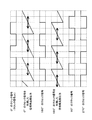
- FIG. 3 shows the output characteristics of a phase detector such as the phase detector 13 or 23.
- the phase detection unit having the output characteristics of FIG. 3 reduces the voltage value of its output signal to a predetermined lower limit voltage value ( For example, the voltage is increased from 0 volts to a predetermined upper limit voltage value (for example, 5 volts).
- the detection range of the phase difference is limited to a range from 0 ° to 360 °, and a discontinuity of one clock occurs at the limit point of the detection range. That is, as shown in FIG.
- the voltage value of the output signal of the phase detector is the same when the phase difference between the first and second comparison signals is 0 ° and when it is 360 ° (phase difference). Since the voltage value of the output signal of the phase detector changes from the vicinity of the upper limit voltage value to the lower limit voltage value when the angle reaches 360 ° from less than 360 °, the phase difference between the first and second comparison signals is zero. When the angle is near ° or around 360 °, jitter of one clock may occur in the derived time interval T INT .
- phase difference between the first and second comparison signals is actually 0.1 °, but the phase difference is detected to be 359.9 ° due to the influence of the detection error, the derivation is performed.
- Time interval T INT deviates from the true time interval T INT by nearly one clock.
- the linearity with respect to the phase of the output signal (output voltage) of the phase detector deteriorates.
- broken-line ellipse portions 91 and 92 correspond to portions where the linearity is not good.
- the clock signal clk is referred to as a 0 ° clock signal.
- the phase of the clock signal clk is changed in the time measuring device of the second embodiment.
- a signal obtained by inverting the clock signal clk that is, a clock signal formed by advancing the phase of the clock signal clk by 180 ° is referred to as a 180 ° clock signal.
- a clock signal formed by advancing the phase of the clock signal clk by 90 ° is called a 90 ° clock signal.
- a clock signal formed by further advancing the phase of the 180 ° clock signal by 90 ° is referred to as a 270 ° clock signal.
- the first comparison signal (for example, the signal S BPFA2 in FIG. 2) based on the input timing of the start trigger signal has a phase from 90 ° to 270 ° when viewed from the 0 ° clock signal.
- the phase ⁇ str is detected using the 0 ° clock signal as the second comparison signal (reference signal). Otherwise, the 180 ° clock signal is used as the second comparison signal (reference signal).
- the phase ⁇ str is detected.
- the stop trigger signal By doing in this way, the output signal of a phase detection part is always limited within the range of the line segment with an arrow of FIG.
- FIG. 5 is a block diagram of a time measuring apparatus according to the second embodiment.
- the time measuring apparatus of FIG. 5 includes each part referred to by reference numerals 100, 200, 300, 400, 510, 520, 600 and 700.
- the start trigger signal trig_str is input to the start side phase detection unit 100 via the signal distributor 510, and the stop trigger signal trig_stp is input to the stop side phase detection unit 200 via the signal distributor 520.
- the signal distributor 510 supplies the start trigger signal trig_str to the start trigger detection unit 600 with a signal with a reduced signal strength, that is, a start trigger signal trig_str ′ with a reduced signal strength.
- the signal distributor 520 supplies the stop trigger signal detecting unit 700 with a signal obtained by reducing the signal strength of the stop trigger signal trig_stp, that is, the stop trigger signal trig_stp ′ having a reduced signal strength.
- Signal distributors 510 and 520 are used for signal distribution.
- the signal-to-noise ratio can be improved by increasing the signal strength of the input signals (trig_str, trig_stp).
- the signal distributors 510 and 520 may be provided with attenuators for logic signals.
- the signal strength of the start trigger signal and the stop trigger signal may be reduced inside the start side trigger detection unit 600 and the stop side trigger detection unit 700 (in this case, the signal strength in the signal distributors 510 and 520 is reduced). Function can be removed).
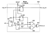
- FIG. 6 is an internal configuration diagram of the start side trigger detection unit 600.
- the start-side trigger detection unit 600 includes each part referred to by reference numerals 601 to 607.
- the phase converter 601 receives the clock signal clk, outputs a 0 ° clock signal, which is the clock signal clk itself, as a clock signal 621, and a 90 ° clock signal obtained by advancing the phase of the clock signal clk by 90 °. Is generated and output as a clock signal 622.
- the phase converter 602 receives the clock signal 621, outputs a 0 ° clock signal, which is the clock signal 621 itself, as the clock signal 623, and advances the phase of the clock signal 621 by 180 ° (ie, the clock signal).
- a 180 ° clock signal (inverted 621) is generated and output as a clock signal 624.
- the flip-flops 603 and 604 are D-type flip-flops (hereinafter referred to as DFF).
- the DFF includes a clock terminal, a D terminal, a Q terminal, and a reset terminal.
- the DFF holds the level (logical value) of the signal input to the D terminal at the up edge timing of the signal supplied to the clock terminal, and a signal having the held signal level (logical value). Output from Q terminal.
- the high level reset signal RESET is supplied to the reset terminal of the DFF, the holding is canceled and the output signal of the DFF Q terminal becomes the low level.
- the arithmetic unit 400 (see FIG. 5) can supply a high-level reset signal RESET to each part in the time measuring device at an arbitrary timing. In the present embodiment, it is assumed that the high-level reset signal RESET is not supplied from the arithmetic unit 400 to each part in the time measuring device unless otherwise specified.
- the start trigger signal trig_str ′ and the clock signal 622 are input to the D terminal and the clock terminal of the DFF 603, respectively.
- An output signal from the Q terminal of the DFF 603 is output to the outside of the detection unit 600 as a start trigger signal L_trig_str latched in synchronization with the clock signal 622.
- a clock signal 622 and a start trigger signal trig_str ′ are input to the D terminal and the clock terminal of the DFF 604, respectively.
- the logic circuits 605 and 606 are AND circuits (logical product circuits). Each of the AND circuits 605 and 606 is a two-input AND circuit, and thus has first and second input terminals and an output terminal (the same applies to other AND circuits described later).
- the output signal of the Q terminal of the DFF 604 is input as it is to the first input terminal of the AND circuit 606, while the inverted signal of the output signal of the Q terminal of the DFF 604 is input to the first input terminal of the AND circuit 605.
- Clock signals 624 and 623 are input to the second input terminals of the AND circuits 605 and 606, respectively.
- the logic circuit 607 is an OR circuit (OR circuit).
- the OR circuit 607 is a two-input OR circuit, and thus has first and second input terminals and an output terminal (the same applies to other OR circuits described later).
- the output signal of the AND circuit 605 (that is, the logical product signal of the inverted signal of the output signal of the Q terminal of the DFF 604 and the clock signal 624) is input to the first input terminal of the OR circuit 607, and the second input of the OR circuit 607 is input.
- An output signal of the AND circuit 606 (that is, a logical product signal of the output signal of the Q terminal of the DFF 604 and the clock signal 623) is input to the terminal.
- one of the clock signals 623 and 624 is output from the output terminal of the OR circuit 607 according to the level of the output signal at the Q terminal of the DFF 604.
- a clock signal output from the output terminal of the OR circuit 607 is referred to as a clock signal clk_str.
- the start-side trigger detection unit 600 includes clock selection units (601, 602, 604 to 607).
- the clock selection unit is based on the timing relationship between the start trigger signal trig_str ′ and the clock signal clk (specifically, based on the relationship between the up edge timing of the start trigger signal trig_str ′ and the up edge timing of the clock signal clk), A clock signal 623 having the same phase as the clock signal clk or a clock signal 624 having a phase different from the clock signal clk is selectively output.
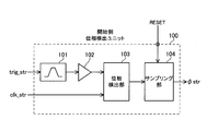
- FIG. 7 is an internal configuration diagram of the start-side phase detection unit 100.
- the start-side phase detection unit 100 includes each part referred to by reference numerals 101 to 104, and detects and outputs the phase ⁇ str of the start trigger signal trig_str.
- the phase ⁇ str detected by the unit 100 is the phase of the start trigger signal trig_str based on the clock signal clk_str (in other words, the phase of the clock signal clk_str at the timing when the start trigger signal trig_str is input to the time measurement device). ). That is, (see FIG.
- the phase ⁇ str detected by the unit 100 is the up edge immediately before the clock signal clk_str viewed from the up edge timing t A of the signal trig_str and the up edge timing t A of the signal trig_str.
- the phase ⁇ str is 0 °.
- the BPF 101 is the same as the BPF 11 (see FIG. 1) of the first embodiment. Therefore, the BPF 101 generates and outputs a sinusoidal signal S BPFA1 (see FIG. 2) by extracting the signal component of the clock frequency included in the start trigger signal trig_str. As in the first embodiment, in the unit 100, a rectangular wave signal S BPFA2 (see FIG. 2) can be generated from the sine wave signal S BPFA1 using a comparator (not shown).
- the amplifier 102 is an amplifier that includes the function of the limiter 12 of FIG. 1, and makes the amplitude of the output signal of the BPF 101 constant.
- the output signal of the BPF 101 is input to the phase detection unit 103 as the first comparison signal via the amplifier 102.
- the phase detection unit 103 also receives a clock signal clk_str as the second comparison signal. Since the first comparison signal input to the phase detection unit 103 has the same frequency as the clock signal clk_str as the second comparison signal, a phase difference can be defined between the first and second comparison signals.
- the phase detection unit 103 is the same as the phase detection unit 13 of the first embodiment. However, as described above, the second comparison signal for the phase detector 103 is the clock signal clk_str. Therefore, the phase detection unit 103 detects the phase difference between the two signals by comparing the phases of the rectangular wave signal SBPFA2 (see FIG. 2) indicating the clock frequency component of the start trigger signal trig_str and the clock signal clk_str. A voltage signal having a voltage value corresponding to the phase difference is output.
- the rectangular wave signal S BPFA2 may be generated from the sine wave signal S BPFA1 in the phase detection unit 103 or in a preceding circuit of the phase detection unit 103.
- the phase difference detected by the phase detector 103 corresponds to the phase ⁇ str.
- the sampling unit 104 reads the value of the phase ⁇ str by sampling the output voltage signal of the phase detection unit 103, and outputs the read value of the phase ⁇ str (sampling value) to the calculation unit 400.
- the sampling timing in the sampling unit 104 is specified by a sampling timing specifying unit (not shown) in the time measuring device.
- the sampling timing designating unit has a predetermined delay time (for example, a time of (3 ⁇ T RF )) from the up edge timing of the clock signal clk immediately after the up edge timing of the start trigger signal (trig_str, trig_str ′).
- the sampling unit 104 is controlled so that the output voltage signal of the phase detection unit 103 is sampled at the elapsed timing.
- the output signal of the sampling unit 104 shows a predetermined initial value.
- 9 to 12 show the states of input / output signals and internal signals of the start side trigger detection unit 600 in cases A1 to A4, respectively.
- the output signal levels of the DFFs 603 and 604 are set to low level, and then the reset signal RESET is set to low level. Cases A1 to A4 are assumed starting from this stage.
- Cases A1 to A4 are cases where the up-edge timing of the start trigger signal trig_str ′ belongs to the sections P1 to P4, respectively.
- the sections P1, P2, P3, P4 visits.
- the signal level of the signal L_trig_str is the clock signal 622 (90 ° clock signal) after the up-edge timing of the start trigger signal trig_str ′.
- the signal level is switched from the low level to the high level.
- the clock signal clk_str coincides with the 180 ° clock signal before the up-edge timing of the start trigger signal trig_str ′, but after the up-edge timing of the start trigger signal trig_str ′, the 0 ° clock signal and the 180 ° clock signal Either.
- the clock signal clk_str after the up edge timing of the start trigger signal trig_str ′ becomes a 0 ° clock signal in cases A2 and A3, and becomes a 180 ° clock signal in cases A1 and A4.
- the start-side phase detection unit 100 detects the phase ⁇ str using the 0 ° clock signal as the second comparison signal (reference signal) in case A2 and case A3, and 180 ° in case A1 and case A4.
- the phase ⁇ str is detected using the clock signal of ° as the second comparison signal (reference signal). Therefore, it is possible to detect the phase ⁇ str in a portion with good linearity while avoiding the occurrence of the jitter.
- FIG. 13 is an internal configuration diagram of the stop-side trigger detection unit 700.
- the stop-side trigger detection unit 700 includes each part referred to by reference numerals 701 to 707.
- the phase conversion unit 701 is supplied with the clock signal clk_str, outputs the clock signal clk_str itself as the clock signal 721, and generates and outputs a clock signal obtained by advancing the phase of the clock signal clk_str by 90 ° as the clock signal 722. Since the clock signal clk_str is a 0 ° or 180 ° clock signal, the clock signal 722 is a 90 ° or 270 ° clock signal.
- the phase converter 702 receives the clock signal 721, outputs the clock signal 721 itself as the clock signal 723, and advances the phase of the clock signal 721 by 180 ° (that is, the clock signal 721 is inverted). The signal is generated and output as a clock signal 724.
- the stop trigger signal trig_stp ′ and the clock signal 722 are input to the D terminal and the clock terminal of the DFF 703, respectively.
- An output signal from the Q terminal of the DFF 703 is output to the outside of the detection unit 700 as a stop trigger signal L_trig_stp latched in synchronization with the clock signal 722.
- a clock signal 722 and a stop trigger signal trig_stp ′ are input to the D terminal and the clock terminal of the DFF 704, respectively.
- the logic circuits 705 and 706 are AND circuits (logical product circuits).
- the output signal of the Q terminal of the DFF 704 is input as it is to the first input terminal of the AND circuit 706, while the inverted signal of the output signal of the Q terminal of the DFF 704 is input to the first input terminal of the AND circuit 705.
- Clock signals 724 and 723 are input to the second input terminals of the AND circuits 705 and 706, respectively.
- the logic circuit 707 is an OR circuit (OR circuit).
- the output signal of the AND circuit 705 (that is, the logical product signal of the inverted signal of the output signal of the Q terminal of the DFF 704 and the clock signal 724) is input to the first input terminal of the OR circuit 707, and the second input of the OR circuit 707 is input.
- An output signal of the AND circuit 706 (that is, a logical product signal of the output signal of the Q terminal of the DFF 704 and the clock signal 723) is input to the terminal.
- one of the clock signals 723 and 724 is output from the output terminal of the OR circuit 707 according to the level of the output signal from the Q terminal of the DFF 704.
- a clock signal output from the output terminal of the OR circuit 707 is referred to as a clock signal clk_stp.
- An output signal from the Q terminal of the DFF 704 is output to the outside of the detection unit 700 as a latch state signal L_stat.
- the stop-side trigger detection unit 700 has clock selection units (701, 702, 704 to 707).
- the clock selection unit is based on the timing relationship between the stop trigger signal trig_stp ′ and the clock signal clk_str (specifically, based on the relationship between the up edge timing of the stop trigger signal trig_stp ′ and the up edge timing of the clock signal clk_str), A clock signal 723 having the same phase as that of the clock signal clk_str or a clock signal 724 having a phase different from that of the clock signal clk_str is selectively output.
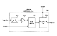
- FIG. 14 is an internal configuration diagram of the stop-side phase detection unit 200.
- the stop-side phase detection unit 200 includes portions referred to by reference numerals 201 to 204, and detects and outputs the phase ⁇ stp of the stop trigger signal trig_stp.
- the phase ⁇ stp detected by the unit 200 is the phase of the stop trigger signal trig_stp with reference to the clock signal clk_stp (in other words, the phase of the clock signal clk_stp at the timing when the stop trigger signal trig_stp is input to the time measuring device). ). That is, (see FIG.
- the phase ⁇ stp detected by the unit 200 is the up edge immediately before the clock signal clk_stp as seen from the up edge timing t B of the signal trig_stp and the up edge timing t B of the signal trig_stp.
- the phase ⁇ stp is 0 °.
- the BPF 201 is the same as the BPF 21 (see FIG. 1) of the first embodiment. Therefore, the BPF 201 generates and outputs a sinusoidal signal S BPFB1 (see FIG. 2) by extracting the signal component of the clock frequency included in the stop trigger signal trig_stp. As in the first embodiment, in the unit 200, a rectangular wave signal S BPFB2 (see FIG. 2) can be generated from the sine wave signal S BPFB1 using a comparator (not shown).
- the amplifier 202 is an amplifier that includes the function of the limiter 22 of FIG. 1, and makes the amplitude of the output signal of the BPF 201 constant.
- the output signal of the BPF 201 is input to the phase detection unit 203 as the first comparison signal via the amplifier 202.
- the phase detection unit 203 also receives the clock signal clk_stp as the second comparison signal. Since the first comparison signal input to the phase detection unit 203 has the same frequency as the clock signal clk_stp as the second comparison signal, a phase difference can be defined between the first and second comparison signals.
- the phase detection unit 203 is the same as the phase detection unit 23 of the first embodiment. However, as described above, the second comparison signal for the phase detector 203 is the clock signal clk_stp. Therefore, the phase detection unit 203 detects the phase difference between the two signals by comparing the phases of the rectangular wave signal S BPFB2 (see FIG. 2) indicating the clock frequency component of the stop trigger signal trig_stp and the clock signal clk_stp. A voltage signal having a voltage value corresponding to the phase difference is output.
- the rectangular wave signal S BPFB2 may be generated from the sine wave signal S BPFB1 in the phase detection unit 203 or in the preceding circuit of the phase detection unit 203.
- the phase difference detected by the phase detector 203 corresponds to the phase ⁇ stp.
- the sampling unit 204 reads the value of the phase ⁇ stp by sampling the output voltage signal of the phase detection unit 203, and outputs the read value of the phase ⁇ stp (sampling value) to the calculation unit 400.
- the sampling timing in the sampling unit 204 is specified by a sampling timing specifying unit (not shown) in the time measuring device.
- the sampling timing designating unit has a predetermined delay time (for example, a time of (3 ⁇ T RF )) from the up edge timing of the clock signal clk immediately after the up edge timing of the stop trigger signal (trig_stp, trig_stp ′).
- the sampling unit 204 is controlled so that the output voltage signal of the phase detection unit 203 is sampled at the elapsed timing.
- the output signal of the sampling unit 204 shows a predetermined initial value.
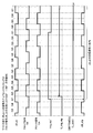
- FIGS. 15 to 18 show the states of input / output signals and internal signals of the stop-side trigger detection unit 700 in cases B1 to B4, respectively.
- the output signal levels of the DFFs 703 and 704 are set to low level, and then the reset signal RESET is set to low level. Cases B1 to B4 are assumed starting from this stage.
- Cases B1 to B4 are cases in which the up edge timing of the stop trigger signal trig_stp ′ belongs to the sections Q1 to Q4, respectively.
- the inequalities “0 ⁇ ⁇ clk_str ⁇ 90”, “90 ⁇ ⁇ clk_str ⁇ 180”, “180 ⁇ ⁇ clk_str ⁇ 270”, “270 ⁇ ⁇ clk_str ⁇ 360 is established (the unit of each inequality is degrees). That is, four sections are formed when the section between two consecutive up-edge trigger timings in the clock signal clk_str is divided into four equal parts. Among the four sections, the sections Q1, Q2, Q3, Q4 visit.
- the signal level of the signal L_trig_stp is first low after the up edge timing of the stop trigger signal trig_stp ′. At the timing of transition from the level to the high level, the low level is switched to the high level.
- the clock signal clk_stp matches the inverted signal of the clock signal clk_str before the up edge timing of the stop trigger signal trig_stp ′, but after the up edge timing of the stop trigger signal trig_stp ′, Either.
- the clock signal clk_stp after the up edge timing of the stop trigger signal trig_stp ′ matches the clock signal clk_str in cases B2 and B3, and matches the inverted signal of the clock signal clk_str in cases B1 and B4.
- the stop-side phase detection unit 200 detects the phase ⁇ stp using the clock signal clk_str as the second comparison signal (reference signal) in the cases B2 and B3, and the clock signal clk_str in the cases B1 and B4. Is used as the second comparison signal to detect the phase ⁇ stp. Therefore, it is possible to detect the phase ⁇ stp in a portion having good linearity while avoiding the occurrence of the jitter.
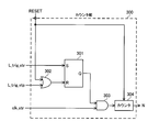
- FIG. 19 is an internal configuration diagram of the counter unit 300.
- the counter unit 300 detects the time interval T INT using the clock cycle TRF as a unit (minimum unit).
- the counter unit 300 includes each part referred to by reference numerals 301 to 304.
- the counter unit 300 uses the clock signal clk_str from the start side trigger detection unit 600, the latched start trigger signal L_trig_str, and the latched stop trigger signal L_trig_stp from the stop side trigger detection unit 700 to start the trigger signal L_trig_str. And the clock number N of the clock signal between the input timings of the stop trigger signal L_trig_stp is counted.
- the clock number N counted by the counter unit 300 is the clock number of the clock signal clk_str. More specifically, the counter unit 300 counts how many up edges of the clock signal clk_str exist after the up edge timing of the start trigger signal L_trig_str and before the up edge timing of the stop trigger signal L_trig_stp. The counted value is detected as the clock number N.
- the flip-flop 301 is an RS flip-flop (hereinafter referred to as RSFF).
- the RSFF has a set terminal, a reset terminal, and a Q terminal.
- the RSFF when the input signals to the set terminal and the reset terminal are high level and low level, respectively, the output signal from the Q terminal is maintained at high level, and the input signals to the set terminal and reset terminal are respectively When the level is low or high, the output signal from the Q terminal is maintained at a low level, and when both the input signals to the set terminal and the reset terminal are at low level, the output signal level at the Q terminal does not change.
- the RSFF 301 is formed so that the output signal level of the Q terminal becomes a low level without depending on the input signal level to the set terminal. .
- the OR circuit 302 inputs a logical sum signal of the reset signal RESET from the arithmetic unit 400 and the latched stop trigger signal L_trig_stp to the reset terminal of the RSFF 301.
- the latched start trigger signal L_trig_str is input to the set terminal of the RSFF 301.
- the AND circuit 303 inputs a logical product signal of the output signal from the Q terminal of the RSFF 301 and the clock signal clk_str to the counter 304. Therefore, the clock signal clk_str is input from the AND circuit 303 to the counter 304 between the up edge timings of the signals L_trig_str and L_trig_stp.
- the counter 304 counts the number of up edges in the signal input from the AND circuit 303 and outputs the counted value as the clock number N. As a result, the number of up edges of the clock signal clk_str between the up edge timings of the signals L_trig_str and L_trig_stp is detected as the count number N.
- the arithmetic unit 400 supplies the high level reset signal RESET to the counter unit 300 so that the signal held and output by the RSFF 301 is set to the low level.
- the counter 304 is initialized (the count value N of the counter 304 is initialized to zero).
- the start trigger signal trig_str and the stop trigger signal trig_stp are sequentially input to the time measuring device in a state where the arithmetic unit 400 sets the reset signal RESET to a low level.
- the arithmetic unit 400 includes an arithmetic device such as a microcomputer, and includes the phases ⁇ str and ⁇ stp detected by the units 100 and 200 (that is, the values of the phases ⁇ str and ⁇ stp given from the sampling units 104 and 204) and the counter unit 300.
- the time interval T INT is obtained with a resolution smaller than the clock cycle T RF based on the count number N detected in step (1).
- the definition of the time interval T INT is as described in the first embodiment. That is, the time interval T INT is the time difference between the rising edge timing t B between the rising edge timing t A of the start trigger signal trig_str stop trigger signal Trig_stp (see FIG. 2).
- the calculation unit 400 obtains the time interval T INT according to the following equation (2).
- T INT T RF ⁇ (N + INVL_stat / 2) + T RF ⁇ ( ⁇ stp ⁇ str) / 360 ... (2)
- the right side of Expression (2) is obtained by adding “T RF ⁇ INVL_stat / 2” to the right side of Expression (1) described in the first embodiment.
- “INVL_stat” in equation (2) has an inverted value of the logical value of the latch state signal L_stat (the same applies to equation (2a) described later).
- the latch state signal L_stat that determines the value of “INVL_stat” is the latch state signal L_stat output from the Q terminal after the DFF 704 in FIG. 13 latches the input signal at the D terminal at the up-edge timing of the stop trigger signal trig_stp ′. It is.
- the second embodiment similarly to the first embodiment, it is possible to measure the time interval between trigger signals with high time resolution, which is difficult to realize with the conventional configuration of FIG. In addition, it is possible to reliably avoid the occurrence of jitter for one clock and to detect the phases ⁇ str and ⁇ stp in a portion having good linearity without depending on the input timing of the start trigger signal trig_str and the stop trigger signal trig_stp. Highly accurate time interval measurement is guaranteed.
- the start-side phase detection unit 100 and the start-side trigger detection unit 600 can be omitted from the time measuring device.
- the signals clk and trig_str ′ themselves are handled as the signals clk_str and L_trig_str, respectively, and supplied to the counter unit 300 and the stop-side trigger detection unit 700, and the calculation unit 400 obtains the time interval T INT according to the equation (2a).
- T INT T RF ⁇ (N + INVL_stat / 2) + T RF ⁇ ⁇ stp / 360 ... (2a)
- the stop trigger signal trig_stp is synchronized with the 180 ° clock signal, that is, the up edge of the clock signal whose stop edge signal t B is 180 °.
- the stop-side phase detection unit 200 and the stop-side trigger detection unit 700 can be omitted from the time measurement device.
- the clock signal clk is input to the counter unit 300 instead of the clock signal clk_str, and the signal trig_stp (or trig_stp ′) is input instead of the signal L_trig_stp.
- the start-side phase detection unit 100 is supplied with the clock signal clk_str so that the phase reading range is 90 ° to 270 °.
- the arithmetic unit 400 may obtain the time interval T INT according to the equation (2b).
- the counter section 300 (counter 304) is intended to count the rising edge of the clock signal clk_str at the timing t B.
- INVL_stat in equation (2b) is the logical value of the signal output from the Q terminal of the DFF 604 after the DFF 604 in FIG. 6 latches the input signal 622 at the D terminal at the up-edge timing of the start trigger signal trig_str ′.
- INVL_stat in equation (2b) has a value of zero when the signal is high level
- INVL_stat of equation (2b) has a value of 1 when the signal is low level
- T INT T RF ⁇ (N ⁇ INVL_stat / 2) ⁇ T RF ⁇ (360 ⁇ str) / 360 ...
- the time measuring apparatus having the configuration J 1 measures the time interval (T INT ) of the input timings (t A , t B ) of the first target signal and the second target signal each having a pulse shape.
- a time measurement device wherein a clock signal having a predetermined clock frequency and clock cycle is used, and a cycle number detection unit (30, 300) for detecting the time interval in units of the clock cycle, and the first and second objects
- a phase detection unit that includes a band-pass filter that receives at least one of the signals as a filter target signal and extracts a signal component of the clock frequency from the filter target signal, and detects a phase difference between the extracted signal and the clock signal Using the unit, the detection result (N) of the cycle number detection unit and the detected phase difference ( ⁇ str, ⁇ stp) by the phase detection unit, a resolution smaller than the clock cycle
- a calculation unit 40, 400 for determining the time interval at.
- the pulsed filter target signal includes signal components of various frequencies including the clock frequency
- the phase difference between the extracted signal and the clock signal represents a time component smaller than the clock cycle in the time interval
- the detection result of the cycle number detection unit and the phase difference detected by the phase detection unit The time interval can be obtained with a resolution smaller than the clock cycle.
- the first and second target signals in the first and second embodiments can be considered as a start trigger signal and a stop trigger signal.
- both the start trigger signal trig_str and the start trigger signal trig_str ′ in which the signal strength is reduced belong to the first target signal
- the stop trigger signal trig_stp ′ is also the second in the stop trigger signal trig_stp ′ in which the signal strength is reduced. It belongs to the target signal.
- the start trigger signal and the stop trigger signal are synchronized with the clock signal
- the above equation (1) is used, and the start trigger signal as the first and second target signals and Each of the stop trigger signals becomes a filter target signal.
- the time measuring apparatus having a configuration J 9 belonging to configure J 1, wherein the phase detection unit, a first extraction signal a signal component of the clock frequency from the first target signal (trig_str)
- a first phase detection unit (10) having a first bandpass filter (11) for extraction, detecting a phase difference ( ⁇ str) between the first extraction signal and the clock signal, and the second target signal (trig_stp) )
- the above formula (1a) or (1b) can be used. Any one of the signals may be input to the bandpass filter (11 or 21) as a filter target signal.
- the time measuring apparatus having a configuration J 5 belonging to configure J 1, based on the timing relationship between the original clock signal (clk) having a clock frequency and the first target signal, the original clock A first clock selection unit (601, 602, 604 to 607; see FIG. 6) that selectively outputs a clock signal (623 or 624; clk_str) having the same or different phase as the signal, the second target signal and the Based on the timing relationship with the output clock signal (clk_str) of the first clock selection unit, the clock signal (723 or 724; clk_stp) having the same or different phase as the output clock signal (clk_str) of the first clock selection unit is selected.
- the first band-pass filter (101) that extracts the signal component of the clock frequency from the first target signal, and the extracted signal of the first band-pass filter and the output clock signal of the first clock selection unit A first phase detection unit (100) that detects a phase difference ( ⁇ str) from (clk_str), and a second bandpass filter (201) that extracts a signal component of the clock frequency from the second target signal, A second phase detection unit (200) for detecting a phase difference between the extracted signal of the second band pass filter and the output clock signal (clk_stp) of the second clock selection unit, and the calculation unit (400) , Using the detection result (N) of the cycle number detection unit (300) and the detected phase difference ( ⁇ str, ⁇ stp) by the first and second phase detection units, It can be determined the time interval (T INT) at the resolution.
- first and second clock selectors By providing the first and second clock selectors and configuring the first and second phase detection units as described above, it becomes possible to selectively use a clock signal having a phase suitable for phase difference detection. . As a result, the occurrence of jitter for one clock can be avoided, and the phase difference ( ⁇ str, ⁇ stp) can be detected in a portion with good linearity, so that highly accurate time interval measurement is ensured.
- the time measuring apparatus having a configuration J 6 belonging to configure J 5, the first clock selection unit (601, 602, 604 to 607; see FIG. 6), the first Based on the timing relationship between one target signal and the original clock signal (clk), a clock signal (623 or 624; clk_str) having the same phase as the original clock signal or having the phase of the original clock signal inverted is selected.
- the second clock selection unit (701, 702, 704 to 707; see FIG. 13) outputs a timing relationship between the second target signal and the output clock signal (clk_str) of the first clock selection unit. Based on the clock signal having the same phase as the output clock signal of the first clock selection unit or the phase of the output clock signal of the first clock selection unit inverted ( 23 or 724; clk_stp) can be output selectively to.
- the time interval (T INT ) to be measured is determined so that the signal level of the first target signal is predetermined.
- the time between the timing (T A ) when the first level transitions to the predetermined second level and the timing (T B ) when the signal level of the second target signal transitions from the first level to the second level The first clock selection unit (601, 602, 604 to 607; see FIG. 6) is a timing at which the signal level of the first target signal transitions from the first level to the second level (see FIG. 6).
- the timing at which the signal level of the signal transitions from the first level to the second level is the phase of the output clock signal (clk_str) of the first clock selection unit.
- the first clock selection unit outputs a clock signal (0 ° clock signal) having the same phase as the original clock signal.
- the phase difference ( ⁇ str) detected by one phase detection unit belongs to the range of 90 ° to 270 °. This is because the first phase detection unit detects the phase difference ( ⁇ str) using the output clock signal of the first clock selection unit (clock signal of 0 °, that is, clk).
- the first clock selection unit outputs a clock signal (180 ° clock signal) obtained by inverting the phase of the original clock signal.
- the phase difference ( ⁇ str) detected by the first phase detection unit belongs to the range of 90 ° to 270 °. This is because the first phase detection unit detects the phase difference ( ⁇ str) by using the output clock signal (180 ° clock signal, that is, the inverted signal of clk) of the first clock selection unit.
- phase difference detected by the second phase detecting unit ( ⁇ stp) from 90 ° in the range of 270 °.
- the first and second levels are a high level and a low level, respectively, but their relationship may be reversed. The same can be said for the first embodiment.
- the period number detection unit (300) is configured to output the first target signal and the original clock signal (clk).
- the time interval may be detected in units of the clock period using a signal (L_trig_str) based on the signal and a signal (L_trig_stp) based on the second target signal and the output clock signal (clk_str) of the first clock selection unit.
- the start trigger signal or the stop trigger signal is synchronized with the clock signal clk
- the above formula (2a) or (2b) can be used, and the start trigger Any one of the signal and the stop trigger signal may be input to the bandpass filter (101 or 201) as a filter target signal.
- the time measuring device of configuration J 2 belonging to configuration J 1 is the reference clock signal (start trigger signal or stop trigger signal) and the reference clock signal having the clock frequency ( clk or clk_str) based on the timing relationship, a clock selection unit (601, 602 and 604 to 607 in FIG.
- the phase detection unit (100 or 200) includes an extraction signal of the bandpass filter (101 or 201) and an output clock signal (clk_str or clk_stp) of the clock selection unit; It is preferable to detect the phase difference ( ⁇ str or ⁇ stp).
- the clock selection unit By providing the clock selection unit and configuring the phase detection unit as described above, it is possible to selectively use a clock signal having a phase suitable for detecting a phase difference. As a result, the occurrence of jitter for one clock can be avoided, and the phase difference ( ⁇ str or ⁇ stp) can be detected in a portion with good linearity, so that highly accurate time interval measurement is ensured.
- the clock selection unit is configured to generate the reference clock based on the timing relationship.
- a clock signal (623 or 723) having the same phase as the signal (clk or clk_str) or a clock signal (624 or 724) obtained by inverting the phase of the reference clock signal may be selectively output.
- the time interval (T INT ) to be measured has a predetermined signal level of the first target signal.
- the time between the timing (t A ) at which the first level transitions to the predetermined second level and the timing (t B ) at which the signal level of the second target signal transitions from the first level to the second level is the reference clock signal (clk or clk_str) when it falls within the range of 90 ° to 270 ° (cases A2 and A3, or cases B2 and B3), the clock signal having the same phase as the reference clock signal While output, otherwise (case A1 and A4, or, case B1 and B4), it is preferable to output a clock signal obtained by inverting the phase of the reference clock signal.
- the time measuring apparatus of the present invention can be used for measuring and controlling the operation interval of a beam chopper that operates in a pulse in an X-ray free electron laser accelerator, and for measuring and controlling the time interval between pump light and probe light in the pump-probe method.
- the time measuring apparatus of the present invention can be applied to the time interval measurement between any two pulse signals.
Landscapes
- Physics & Mathematics (AREA)
- General Physics & Mathematics (AREA)
- Nonlinear Science (AREA)
- Measurement Of Unknown Time Intervals (AREA)
- Engineering & Computer Science (AREA)
- Power Engineering (AREA)
- Manipulation Of Pulses (AREA)
Abstract
カウンタ部(30)は、開始トリガ信号及び停止トリガ信号の入力タイミング間の時間間隔をクロック周期の整数倍で検出する。BPF(11、21)は、開始トリガ信号及び停止トリガ信号におけるクロック周波数の信号成分を抽出し、位相検出部(13、23)は、それらの抽出信号とクロック信号との位相差を検出する。演算部(40)は、カウンタ部(30)の検出結果(N)と位相検出部(13、23)の検出位相差(φstr、φstp)に基づき、上記時間間隔(TINT)をクロック周期よりも小さな分解能にて求める。
Description
本発明は、時間測定装置に関する。
開始トリガ信号と停止トリガ信号の時間間隔を測定する際、開始トリガ信号のアップエッジのタイミング(立ち上がりのタイミング)と停止トリガ信号のアップエッジのタイミングとの間に、基準クロックのゼロクロスが何回あったかをカウンタを用いて計数する。この方式では、基準クロックの周期の整数倍の分解能しか得られない。そこで、クロック周期未満の測定分解能を得るべく様々な方法が提案されている。
図20は、クロック周期未満の測定分解能を得ることが可能な従来の時間測定装置の概略構成図であり、図21は、図20の時間測定装置の動作説明図である(例えば特許文献1参照)。図20の時間測定装置では、コンデンサCを予め一定電圧に充電しておく。そして、トリガパルスを受けたタイミングでスイッチSWをオンにしてコンデンサCを定電流回路に接続し、コンデンサCの蓄積電荷の放電を開始する。放電は、トリガパルスの後に基準クロックを受けたタイミング(基準クロックのアップエッジタイミング)で、スイッチSWのターンオフにより停止する。放電によるコンデンサCの両極間の電圧変化ΔVをAD変換器により読み取る。定電流回路を用いて放電される積分電荷量は放電時間に比例するため、電圧ΔVは、トリガパルスと基準クロックとの時間差ΔTに対応した値を持つ。故に、電圧ΔVからクロック周期未満の時間間隔についての情報が得られる。
図20の構成では、基準クロックの周期として10ナノ秒程度が採用され(即ちクロック周波数は100MHz程度とされ)、時間間隔の実質的な測定精度(測定分解能)は25ピコ秒程度にとどまる。これは、主として以下の理由によるものである。即ち、スイッチSWのターンオン/ターンオフには、ナノ秒オーダーの時間がかかるので、その時間分、測定分解能が悪くなる。これと関連するが、スイッチSWを含む回路の特性上、コンデンサCの放電の開始直後及び終了直前(図21の破線楕円2011及び2012の部分)においてコンデンサCの電圧低下の直線性が得難く、理想的な電圧情報ΔVを得ることができない。これらの事情により、図20の構成において、クロック周波数を100MHzより高めたとしても、結局、スイッチSWの応答性能やコンデンサ電圧低下の非直線性がボトルネックとなって、時間間隔の実質的な測定精度(測定分解能)を向上させることが難しい。
例えば、X線自由電子レーザ加速器においては、パルス動作するビームチョッパのタイミングを1ピコ秒以下の精度で安定させることが要求され、図20の構成では、このような要求への対応が難しい。
そこで本発明は、2つの信号の時間間隔の測定精度向上に寄与する時間測定装置を提供することを目的とする。
本発明に係る時間測定装置は、各々がパルス状の第1対象信号及び第2対象信号の入力タイミングの時間間隔を測定する時間測定装置であって、所定のクロック周波数及びクロック周期のクロック信号を用い、前記クロック周期を単位として前記時間間隔を検出する周期数検出部と、前記第1及び第2対象信号の内の少なくとも一方をフィルタ対象信号として受けて前記フィルタ対象信号から前記クロック周波数の信号成分を抽出するバンドパスフィルタを有し、その抽出信号と前記クロック信号との位相差を検出する位相検出ユニットと、前記周期数検出部の検出結果と前記位相検出ユニットによる検出位相差を用い、前記クロック周期よりも小さな分解能にて前記時間間隔を求める演算部と、を備えたことを特徴とする。
パルス状のフィルタ対象信号はクロック周波数を含む様々な周波数の信号成分を内包しているため、バンドパスフィルタを用いることで、フィルタ対象信号からクロック周波数の信号成分を抽出することが可能である。この抽出信号とクロック信号との位相差は、前記時間間隔の内の、前記クロック周期よりも小さな時間成分を表しているため、前記周期数検出部の検出結果と前記位相検出ユニットによる検出位相差を用いれば、前記クロック周期よりも小さな分解能にて前記時間間隔を求めることが可能である。前記時間間隔の内の、前記クロック周期よりも小さな時間成分を測定するに際し、スイッチSW(図20)のような部品に頼る必要がないため、当該時間間隔を高精度で測定することが可能となる。
本発明によれば、そこで本発明は、2つの信号の時間間隔の測定精度向上に寄与する時間測定装置を提供することが可能である。
以下、本発明の実施形態の例を、図面を参照して具体的に説明する。参照される各図において、同一の部分には同一の符号を付し、同一の部分に関する重複する説明を原則として省略する。尚、本明細書では、記述の簡略化上、情報、信号、物理量又は部材等を参照する記号又は符号を記すことによって、該記号又は符号に対応する情報、信号、物理量又は部材等の名称を省略又は略記することがある。
<<第1実施形態>>
本発明の第1実施形態を説明する。図1は、第1実施形態に係る時間測定装置(時間間隔測定装置)のブロック図である。図1の時間測定装置は、符号10、20、30、40、51及び52によって参照される各部位を備える。
本発明の第1実施形態を説明する。図1は、第1実施形態に係る時間測定装置(時間間隔測定装置)のブロック図である。図1の時間測定装置は、符号10、20、30、40、51及び52によって参照される各部位を備える。
時間測定装置で取り扱われる任意の矩形波の信号(クロック信号のようなデジタル信号を含む)は、電圧信号であって、ローレベル又はローレベルよりも高いハイレベルの信号レベルを択一的にとる。矩形波の信号(クロック信号のようなデジタル信号を含む)において、信号レベルのローレベルからハイレベルへの遷移をアップエッジと表現し、その遷移のタイミングをアップエッジタイミングと表現する。
時間測定装置には、開始トリガ信号trig_str及び停止トリガ信号trig_stpが入力されると共に、所定のクロック周波数及びクロック周期TRFを有するクロック信号clkが入力される。開始トリガ信号trig_str及び停止トリガ信号trig_stpの夫々は、パルス状の矩形波信号である。クロック信号clkを発生するクロック発生器(不図示)が時間測定装置に内包されていても良い。停止トリガ信号trig_stpは、開始トリガ信号trig_strよりも後に時間測定装置に入力される。本実施形態において、クロック信号clkのクロック周波数は5.7GHz(ギガヘルツ)であるとする。従って、クロック周期TRFは約175ピコ秒である。
開始トリガ信号trig_strは、信号分配器51を介して開始側位相検出ユニット10に入力され、停止トリガ信号trig_stpは、信号分配器52を介して停止側位相検出ユニット20に入力される。信号分配器51は、開始トリガ信号trig_strの信号強度を低減させた信号、即ち、信号強度が低減された開始トリガ信号trig_str'をカウンタ部30に供給する。信号分配器52は、停止トリガ信号trig_stpの信号強度を低減させた信号、即ち、信号強度が低減された停止トリガ信号trig_stp'をカウンタ部30に供給する。信号分配器51及び52は信号の分配に使用される。後述のバンドパスフィルタの出力信号強度が低い場合には、入力信号(trig_str、trig_stp)の信号強度を大きくすることで信号対雑音比を向上することが可能である。このときには、信号分配器51及び52に論理信号用の減衰器を設けると良い。或いは、カウンタ部30の内部にて開始トリガ信号及び停止トリガ信号の信号強度を低減させても良い(この場合、信号分配器51及び52における信号強度の低減機能は削除され得る)。
開始側位相検出ユニット10は、クロック信号clkを基準とした開始トリガ信号trig_strの位相φstr(換言すれば、開始トリガ信号trig_strが時間測定装置に入力されたタイミングにおけるクロック信号clkの位相φstr)を検出及び出力する。停止側位相検出ユニット20は、クロック信号clkを基準とした停止トリガ信号trig_stpの位相φstp(換言すれば、停止トリガ信号trig_stpが時間測定装置に入力されたタイミングにおけるクロック信号clkの位相φstp)を検出及び出力する。本実施形態では、位相φstr及びφstpの単位を度にて表す。つまり、位相φstr及びφstpの夫々は、0°から360°までの何れかの値をとる。クロック信号clkを含む任意のクロック信号の位相も0°から360°までの何れかの値をとる。任意のクロック信号に関し、当該クロック信号のアップエッジタイミングにおいて当該クロック信号の位相が0°であると考える。
図2に、時間測定装置内の各部の信号波形を示す。位相φstrは、信号trig_strのアップエッジタイミングtAと、信号trig_strのアップエッジタイミングtAから見たクロック信号clkの直前のアップエッジタイミングtA’との時間差TDIFAに対し、“360/TRF”を乗じたものであり、“φstr=360×TDIFA/TRF”にて表される。但し、信号trig_strのアップエッジタイミングtAと、クロック信号clkの或るアップエッジタイミングとが完全に一致している場合、位相φstrは0°である。尚、本実施形態では、開始トリガ信号trig_strのパルス幅(信号trig_strがハイレベルとなる区間)は、クロック周期TRFの3倍であると仮定している(停止トリガ信号についても同様)。
位相φstpは、信号trig_stpのアップエッジタイミングtBと、信号trig_stpのアップエッジタイミングtBから見たクロック信号clkの直前のアップエッジタイミングtB’との時間差TDIFBに対し、“360/TRF”を乗じたものであり、“φstp=360×TDIFB/TRF”にて表される。但し、信号trig_stpのアップエッジタイミングtBと、クロック信号clkにおける或るアップエッジタイミングとが完全に一致している場合、位相φstpは0°である。
時間測定装置は、時間測定装置に対する開始トリガ信号trig_str及び停止トリガ信号trig_stpの入力タイミングの時間間隔TINTを求めることができる。時間測定装置に対する開始トリガ信号trig_str及び停止トリガ信号trig_stpの入力タイミングは、夫々、タイミングtA及びtBである。つまり、時間間隔TINTはタイミングtA及びtB間の時間差を表す。
カウンタ部30は、信号trig_str'及びtrig_stp'とクロック信号clkとを用いて、開始トリガ信号及び停止トリガ信号の入力タイミング間におけるクロック信号clkのクロック数Nを計数する。より具体的には、カウンタ部30は、タイミングtAより後であって且つタイミングtBより前に、クロック信号clkのアップエッジが幾つ存在するかをカウントし、カウントした値をクロック数Nとして検出する。つまり、カウンタ部30は、クロック周期TRFを単位(最小単位)として時間間隔TINTを検出し、カウンタ部30にて検出される時間間隔TINTは(TRF×N)となる。図2の例において“N=8”である。図2の信号SNはカウンタ部30の内部信号であり、信号SN中のクロック数にて値Nが決定される。
カウンタ部30に用いられるクロック信号の周波数として5.7GHzという高い周波数を用いることにより、カウンタ部30における時間分解能を高めることができる。図20に対応する従来構成では、100MHz(メガヘルツ)程度のクロック信号が用いられており、即ち、本実施形態で使用するクロック周波数よりも1/57程度の低い周波数が用いられており、結果、時間分解能が高くない。本実施形態におけるカウンタ部30は、例えば、高い周波数でも動作可能なフリップフロップをカスケード接続した回路にて実現される。
位相検出ユニット10及び20は、クロック周期より小さな時間分解能を達成するために、BPF(バンドパスフィルタ)11及び21を用いて開始トリガ信号trig_str及び停止トリガ信号trig_stpからクロック周波数(5.7GHz)の信号成分を抽出し、各抽出信号とクロック信号との位相差を検出する。ユニット10及び20の構成及び動作について詳説する。
開始側位相検出ユニット10は、BPF(バンドパスフィルタ)11、リミッタ12、位相検出部13及びサンプリング部14を備える。停止側位相検出ユニット20は、BPF(バンドパスフィルタ)21、リミッタ22、位相検出部23及びサンプリング部24を備える。ユニット10及び20は、入力信号が互いに異なるだけで、互いに同じ構成を有する。
BPF11は、開始トリガ信号trig_strに含まれる、所定の通過帯域内の信号成分を抽出して出力するバンドパスフィルタであり、BPF21は、停止トリガ信号trig_stpに含まれる、所定の通過帯域内の信号成分を抽出して出力するバンドパスフィルタである。上記通過帯域は、BPF11及び12間で共通であり、クロック信号clkのクロック周波数を内包する。上記通過帯域がクロック周波数を内包しつつ、なるだけ狭い帯域となるようにBPF11及び21は形成される。例えば、空洞型BPFにてBPF11及び21を形成することができる。以下では、説明の具体化及び便宜上、特に記述無き限り、BPF11及び21の出力信号がクロック周波数の信号成分(即ち、クロック信号の周波数成分)のみを有していると考える。
図2において、信号SBPFA1はBPF11の出力信号(抽出信号)である。つまり、信号SBPFA1は、BPF11によって開始トリガ信号trig_strから抽出されたクロック周波数成分の信号である。信号SBPFB1はBPF21の出力信号(抽出信号)である。つまり、信号SBPFB1は、BPF21によって停止トリガ信号trig_stpから抽出されたクロック周波数成分の信号である。信号SBPFA1及びSBPFB1の夫々は時間経過と共に振幅が変化する正弦波状の信号であり、その正弦波の周波数はクロック周波数と一致する。
開始トリガ信号trig_str及び停止トリガ信号trig_stpはパルス信号であるため、様々な周波数成分を含んでいる。従って、BPF11及び21によって開始トリガ信号trig_str及び停止トリガ信号trig_stpからクロック信号の周波数成分を抽出すれば、クロック周波数を持つ正弦波状信号SBPFA1及びSBPFB1を得ることができる。図2では、開始トリガ信号trig_strのアップエッジタイミングを起点として、正弦波状信号SBPFA1の振幅が徐々に増大した後に徐々に減少しているが、開始トリガ信号trig_strのアップエッジタイミングを起点とした正弦波状信号SBPFA1の振幅変化の詳細は、BPF11のフィルタ特性に依存する。正弦波状信号SBPFB1についても同様である。
正弦波状信号SBPFA1及びSBPFB1の夫々の信号レベルは、ゼロを基準にして正及び負間を振動する。タイミングtAにおいて信号SBPFA1の正弦波としての位相は0°であり、タイミングtBにおいて信号SBPFB1の正弦波としての位相は0°である。図2において、信号SBPFA2は、正弦波状信号SBPFA1の信号レベルが0又は正であるときにハイレベルとなる一方で正弦波状信号SBPFA1の信号レベルが負であるときにローレベルとなる矩形波状信号であり、信号SBPFB2は、正弦波状信号SBPFB1の信号レベルが0又は正であるときにハイレベルとなる一方で正弦波状信号SBPFB1の信号レベルが負であるときにローレベルとなる矩形波状信号である。ユニット10においてコンパレータ(不図示)を用いて正弦波状信号SBPFA1から矩形波状信号SBPFA2を生成することができ、ユニット20においてコンパレータ(不図示)を用いて正弦波状信号SBPFB1から矩形波状信号SBPFB2を生成することができる。図2においては、正弦波状信号SBPFA1の振幅の増減に伴って矩形波状信号SBPFA2の振幅も増減しているが、実際の矩形波状信号SBPFA2の振幅は一定でありうる(矩形波状信号SBPFB2についても同様)。
リミッタ12は、BPF11の出力信号の振幅を一定にする(BPF11の出力信号の振幅を一定値以下に制限する)リミット処理を実行し、リミッタ22は、BPF21の出力信号の振幅を一定にする(BPF21の出力信号の振幅を一定値以下に制限する)リミット処理を実行する。リミッタ12におけるリミット処理はBPF11の出力信号の増幅機能を含んでいても良く、リミッタ22におけるリミット処理はBPF21の出力信号の増幅機能を含んでいても良い。リミッタ12のリミット処理を経た後のBPF11の出力信号が、第1比較信号として位相検出部13に供給される。リミッタ22のリミット処理を経た後のBPF21の出力信号が、第1比較信号として位相検出部23に供給される。位相検出部(13、23)の位相検出結果は、比較信号の電力に依存することがあるが、リミット処理により、位相検出部の電力依存性の影響が除去される。
位相検出部13及び23の夫々には、第2比較信号(基準信号)として、クロック信号clkが供給される。位相検出部13及び23の夫々に入力される第1比較信号は、第2比較信号としてのクロック信号clkと同じ周波数を有しているため、第1及び第2比較信号間で位相差を定義できる。
位相検出部13及び23の夫々は、第1及び第2比較信号の位相を比較して第1及び第2比較信号間の位相差を検出し、検出位相差に応じた電圧値を有する電圧信号を出力する(後述の他の位相検出部についても同様)。検出される第1及び第2比較信号間の位相差とは、第2比較信号の位相から見た第1比較信号の位相(換言すれば、第2比較信号を基準とした第1比較信号の位相)である。位相検出部13にて検出される位相差が位相φstrに相当し、位相検出部23にて検出される位相差が位相φstpに相当する。
位相検出部13、23における第1比較信号は、夫々、矩形波状信号SBPFA2、SBPFB2であって良い。この場合、位相検出部13、23内にて、又は、位相検出部13、23の前段回路(例えばリミッタ12、22)にて、正弦波状信号SBPFA1、SBPFB1から矩形波状信号SBPFA2、SBPFB2を生成すれば良い。この場合、位相検出部(13、23)はデジタル位相検出部と呼べる。デジタル位相検出部を用いることにより、高い直線性の実現、製品ごとのばらつきの抑制、及び、検出されるべき位相の温度特性の向上を目指す。
尚、位相検出部13は、矩形波状信号SBPFA2の位相とクロック信号clkの位相を比較する際、それらの信号に対し所定のローカル周波数(例えば4.7GHzの周波数)を有するローカル信号を乗算することで(ミキシングすることで)、矩形波状信号SBPFA2及びクロック信号clkの周波数を中間帯域の周波数(例えば1GHzの周波数)にまで落とし、その後に、両信号を比較するようにしても良い。位相検出部23についても同様である。
また、位相検出部13は、正弦波状信号SBPFA1そのものを第1比較信号として用いて、第1及び第2比較信号の位相を比較するようにしても良い。この場合、位相検出部13は、正弦波状信号SBPFA1とクロック信号clkをアナログ乗算器にて乗算し、乗算結果から位相φstrとしての位相差を検出すれば良い。位相検出部23及び第2実施形態にて述べる位相検出部についても同様である。
サンプリング部14は、位相検出部13の出力電圧信号をサンプリングすることで位相φstrの値を読み取り、読み取った位相φstrの値(サンプリング値)を演算部40に出力する。サンプリング部24は、位相検出部23の出力電圧信号をサンプリングすることで位相φstpの値を読み取り、読み取った位相φstpの値(サンプリング値)を演算部40に出力する。
サンプリング部14及び24におけるサンプリングタイミングは、カウンタ部30により指定される。具体的には、カウンタ部30は、自身に入力される開始トリガ信号trig_str'及びクロック信号clkに基づき、開始トリガ信号のアップエッジタイミングtAの直後におけるクロック信号clkのアップエッジタイミングから所定の遅延時間(例えば、(3×TRF)分の時間)が経過したタイミングにおいてサンプリング指示信号SMPstr(図2参照)をサンプリング部14に出力する。同様に、カウンタ部30は、自身に入力される停止トリガ信号trig_stp'及びクロック信号clkに基づき、停止始トリガ信号のアップエッジタイミングtBの直後におけるクロック信号clkのアップエッジタイミングから所定の遅延時間(例えば、(3×TRF)分の時間)が経過したタイミングにおいてサンプリング指示信号SMPstp(図2参照)をサンプリング部24に出力する。サンプリング部14は、サンプリング指示信号SMPstrを受けたタイミングにて位相検出部13の出力電圧信号をサンプリングし、サンプリング部24は、サンプリング指示信号SMPstpを受けたタイミングにて位相検出部23の出力電圧信号をサンプリングする。
開始トリガ信号のアップエッジタイミングの直後におけるBPF11の出力信号は、開始トリガ信号の入力毎にばらつくことも多い。つまり例えば、“或る開始トリガ信号をBPF11に入力したときの、開始トリガ信号のアップエッジタイミングの直後におけるBPF11の出力信号”と、“他の開始トリガ信号をBPF11に入力したときの、開始トリガ信号のアップエッジタイミングの直後におけるBPF11の出力信号”とが互いに大きく異なることがある。BPF21についても同様である。そこで、開始又は停止トリガ信号のアップエッジタイミングから上記遅延時間を経た後にサンプリングを行うようにする。但し、遅延時間が大きすぎると、BPF(11、21)の出力信号におけるクロック周波数の信号成分が減衰しすぎるため、BPF(11、21)のフィルタ特性を考慮しつつ遅延時間を適切に設定しておくと良い。
演算部40は、マイクロコンピュータ等の演算装置から成り、ユニット10及び20にて検出された位相φstr及びφstp(即ち、サンプリング部14及び24から与えられた位相φstr及びφstpの値)並びにカウンタ部30にて検出されたカウント数Nに基づき、クロック周期TRFよりも小さな分解能で時間間隔TINTを求める。具体的には、演算部40は、下記式(1)に従って時間間隔TINTを求める。図2の例では、クロック周期TRFが175ピコ秒であるとすると、クロック数Nは8であり且つ位相φstr及びφstpは夫々90°及び270°であるため、演算部40にて求められる時間間隔TINTは、“TINT=175×8+175×(270-90)/360=1487.5”より、1487.5ピコ秒となる。
TINT=TRF×N+TRF×(φstp-φstr)/360 ・・・(1)
TINT=TRF×N+TRF×(φstp-φstr)/360 ・・・(1)
本実施形態によれば、図20の従来構成では実現困難であった、高時間分解能によるトリガ信号間の時間間隔測定が可能となる。
尚、開始トリガ信号がクロック信号と同期していることが予め決まっている場合、即ち例えば、開始トリガ信号trig_strのアップエッジタイミングtAがクロック信号clkのアップエッジタイミングと一致していることが予め決まっている場合、開始側位相検出ユニット10を時間測定装置から省略することができる。この場合、演算部40は、式(1a)に従って時間間隔TINTを求めれば良い。この際、カウンタ部30は、タイミングtAにおけるクロック信号のアップエッジをカウントしないものとする。
TINT=TRF×N+TRF×φstp/360 ・・・(1a)
TINT=TRF×N+TRF×φstp/360 ・・・(1a)
これに類似して、停止トリガ信号がクロック信号と同期していることが予め決まっている場合、即ち例えば、停止トリガ信号trig_stpのアップエッジタイミングtBがクロック信号clkのアップエッジタイミングと一致していることが予め決まっている場合、停止側位相検出ユニット20を時間測定装置から省略することができる。この場合、演算部40は、式(1b)に従って時間間隔TINTを求めれば良い。この際、カウンタ部30は、タイミングtBにおけるクロック信号のアップエッジをカウントしないものとする。
TINT=TRF×N+TRF×(360-φstr)/360 ・・・(1b)
TINT=TRF×N+TRF×(360-φstr)/360 ・・・(1b)
<<第2実施形態>>
本発明の第2実施形態を説明する。第2実施形態は第1実施形態を基礎とする実施形態であり、第2実施形態において特に述べない事項に関しては、矛盾の無い限り、第1実施形態の記載が第2実施形態にも適用される。
本発明の第2実施形態を説明する。第2実施形態は第1実施形態を基礎とする実施形態であり、第2実施形態において特に述べない事項に関しては、矛盾の無い限り、第1実施形態の記載が第2実施形態にも適用される。
図3は、位相検出部13又は23のような位相検出部の出力特性を表している。図3の出力特性を有する位相検出部は、第1及び第2比較信号間の位相差が0°から360°に向けて増大するにつれて、自身の出力信号の電圧値を所定の下限電圧値(例えば0ボルト)から所定の上限電圧値(例えば5ボルト)に増大させてゆく。但し、原理上、位相差の検出範囲は0°から360°までの範囲に限られ、検出範囲の限界点にて1クロック分の不連続が生じる。つまり、図3に示す如く、第1及び第2比較信号間の位相差が0°である場合と360°である場合とで位相検出部の出力信号の電圧値は同じとなるため(位相差が360°未満から360°に達した時点で位相検出部の出力信号の電圧値は上限電圧値付近から下限電圧値へと変化するため)、第1及び第2比較信号間の位相差が0°付近又は360°付近となる場合には、導出される時間間隔TINTに1クロック分のジッタが発生しうる。
例えば、第1及び第2比較信号間の位相差が実際には0.1°であるのに対し、検出誤差の影響により、その位相差が359.9°であると検出したならば、導出される時間間隔TINTが、真の時間間隔TINTから1クロック近く乖離する。また、回路構成上、第1及び第2比較信号間の位相差が0°付近又は360°付近にあるとき、位相検出部の出力信号(出力電圧)の位相に対する直線性が悪化する。図3において、破線楕円部分91及び92は、当該直線性が良好でない部分に対応する。
第2実施形態では、これらを考慮した時間測定装置の構成を説明する。図4を参照し、本実施形態では、クロック信号clkを0°のクロック信号と呼ぶ。クロック信号clkは、第2実施形態の時間測定装置内で位相が変化せしめられる。クロック信号clkを反転させた信号、即ち、クロック信号clkの位相を180°だけ進めることで形成されるクロック信号を180°のクロック信号と呼ぶ。また、クロック信号clkの位相を90°だけ進めることで形成されるクロック信号を90°のクロック信号と呼ぶ。180°のクロック信号の位相を更に90°だけ進めることで形成されるクロック信号を270°のクロック信号と呼ぶ。
第2実施形態では、開始トリガ信号の入力タイミングに基づく第1比較信号(例えば図2の信号SBPFA2)が、0°のクロック信号から見て90°から270°までの位相を有している場合には、0°のクロック信号を第2比較信号(基準信号)として用いて位相φstrを検出し、そうでない場合には、180°のクロック信号を第2比較信号(基準信号)として用いて位相φstrを検出するようにする。停止トリガ信号についても同様とされる。このようにすることで、位相検出部の出力信号は、常に図4の矢印付き線分の範囲内に限定されるようになる。このため、第1及び第2比較信号間の位相差が0°付近となることによる1クロック分のジッタの発生が抑制されると共に、上記直線性が良好な部分において位相φstr及びφstpを検出することが可能となる。結果、時間測定装置による時間間隔TINTの測定精度向上が図られる。
図5は、第2実施形態に係る時間測定装置のブロック図である。図5の時間測定装置は、符号100、200、300、400、510、520、600及び700によって参照される各部位を備える。
開始トリガ信号trig_strは、信号分配器510を介して開始側位相検出ユニット100に入力され、停止トリガ信号trig_stpは、信号分配器520を介して停止側位相検出ユニット200に入力される。信号分配器510は、開始トリガ信号trig_strの信号強度を低減させた信号、即ち、信号強度が低減された開始トリガ信号trig_str'を開始側トリガ検出部600に供給する。信号分配器520は、停止トリガ信号trig_stpの信号強度を低減させた信号、即ち、信号強度が低減された停止トリガ信号trig_stp'を停止側トリガ検出部700に供給する。信号分配器510及び520は信号の分配に使用される。後述のバンドパスフィルタ(BPF)の出力信号強度が低い場合には、入力信号(trig_str、trig_stp)の信号強度を大きくすることで信号対雑音比を向上することが可能である。このときには、信号分配器510及び520に論理信号用の減衰器を設けると良い。或いは、開始側トリガ検出部600及び停止側トリガ検出部700の内部にて開始トリガ信号及び停止トリガ信号の信号強度を低減させても良い(この場合、信号分配器510及び520における信号強度の低減機能は削除され得る)。
図6は、開始側トリガ検出部600の内部構成図である。開始側トリガ検出部600は、符号601~607によって参照される各部位を備える。位相変換部601は、クロック信号clkの供給を受け、クロック信号clkそのものである0°のクロック信号をクロック信号621として出力すると共に、クロック信号clkの位相を90°だけ進めた90°のクロック信号をクロック信号622として生成及び出力する。位相変換部602は、クロック信号621の供給を受け、クロック信号621そのものである0°のクロック信号をクロック信号623として出力すると共に、クロック信号621の位相を180°だけ進めた(即ち、クロック信号621を反転させた)180°のクロック信号をクロック信号624として生成及び出力する。
フリップフロップ603及び604は、D型フリップフロップ(以下、DFFと表記する)である。DFFは、クロック端子、D端子、Q端子及びリセット端子を備える。周知の如く、DFFは、クロック端子に供給される信号のアップエッジタイミングにてD端子に入力されている信号のレベル(論理値)を保持し、保持した信号レベル(論理値)を有する信号をQ端子から出力する。DFFのリセット端子にハイレベルのリセット信号RESETが供給されたときに当該保持は解消され、DFFのQ端子の出力信号はローレベルとなる。演算部400(図5参照)は、任意のタイミングにおいて、ハイレベルのリセット信号RESETを時間測定装置内の各部位に供給できる。本実施形態では、特に記述無き限り、演算部400からハイレベルのリセット信号RESETが時間測定装置内の各部位に対して供給されていないものとする。
DFF603のD端子及びクロック端子には、夫々、開始トリガ信号trig_str'及びクロック信号622が入力される。DFF603のQ端子からの出力信号は、クロック信号622に同期してラッチされた開始トリガ信号L_trig_strとして、検出部600の外部へと出力される。DFF604のD端子及びクロック端子には、夫々、クロック信号622及び開始トリガ信号trig_str'が入力される。
論理回路605及び606は、AND回路(論理積回路)である。AND回路605及び606の夫々は、2入力のAND回路であり、従って第1及び第2入力端子並びに出力端子を有する(後述の他のAND回路も同様)。AND回路606の第1入力端子にはDFF604のQ端子の出力信号がそのまま入力される一方、AND回路605の第1入力端子にはDFF604のQ端子の出力信号の反転信号が入力される。AND回路605及び606の第2入力端子には、夫々、クロック信号624及び623が入力される。
論理回路607は、OR回路(論理和回路)である。OR回路607は、2入力のOR回路であり、従って第1及び第2入力端子並びに出力端子を有する(後述の他のOR回路も同様)。OR回路607の第1入力端子にはAND回路605の出力信号(即ち、DFF604のQ端子の出力信号の反転信号とクロック信号624との論理積信号)が入力され、OR回路607の第2入力端子にはAND回路606の出力信号(即ち、DFF604のQ端子の出力信号とクロック信号623との論理積信号)が入力される。
結果、DFF604のQ端子の出力信号のレベルに応じ、クロック信号623及び624のどちらかがOR回路607の出力端子より出力されることになる。OR回路607の出力端子より出力されるクロック信号をクロック信号clk_strと呼ぶ。
開始側トリガ検出部600は、クロック選択部(601、602、604~607)を有していると言える。当該クロック選択部は、開始トリガ信号trig_str'とクロック信号clkとのタイミング関係に基づき(詳細には、開始トリガ信号trig_str'のアップエッジタイミングとクロック信号clkのアップエッジタイミングとの関係に基づき)、クロック信号clkと同一の位相を有するクロック信号623又はクロック信号clkと異なる位相を有するクロック信号624を選択的に出力する。
図7は、開始側位相検出ユニット100の内部構成図である。開始側位相検出ユニット100は、符号101~104によって参照される各部位を備え、開始トリガ信号trig_strの位相φstrを検出及び出力する。但し、ユニット100にて検出される位相φstrは、クロック信号clk_strを基準とした開始トリガ信号trig_strの位相(換言すれば、開始トリガ信号trig_strが時間測定装置に入力されたタイミングにおけるクロック信号clk_strの位相)である。つまり(図8(a)参照)、ユニット100にて検出される位相φstrは、信号trig_strのアップエッジタイミングtAと、信号trig_strのアップエッジタイミングtAから見たクロック信号clk_strの直前のアップエッジタイミングtA2’との時間差TDIFA2に対し、“360/TRF”を乗じたものであり、“φstr=360×TDIFA2/TRF”にて表される。但し、信号trig_strのアップエッジタイミングtAと、クロック信号clk_strの或るアップエッジタイミングとが完全に一致している場合、位相φstrは0°である。
BPF101は、第1実施形態のBPF11(図1参照)と同じものである。従って、BPF101は、開始トリガ信号trig_strに含まれるクロック周波数の信号成分を抽出することで正弦波状信号SBPFA1(図2参照)を生成及び出力する。第1実施形態と同様、ユニット100において、コンパレータ(不図示)を用いて正弦波状信号SBPFA1から矩形波状信号SBPFA2(図2参照)を生成することができる。
アンプ102は、図1のリミッタ12の機能を内包する増幅器であり、BPF101の出力信号の振幅を一定にする。BPF101の出力信号は、アンプ102を介し、第1比較信号として位相検出部103に入力される。位相検出部103には、第2比較信号としてクロック信号clk_strも入力される。位相検出部103に入力される第1比較信号は、第2比較信号としてのクロック信号clk_strと同じ周波数を有しているため、第1及び第2比較信号間で位相差を定義できる。
位相検出部103は、第1実施形態の位相検出部13と同じものである。但し、上述したように、位相検出部103にとっての第2比較信号はクロック信号clk_strである。故に、位相検出部103は、開始トリガ信号trig_strのクロック周波数成分を示す矩形波状信号SBPFA2(図2参照)とクロック信号clk_strとの位相を比較して両信号間の位相差を検出し、検出位相差に応じた電圧値を有する電圧信号を出力する。位相検出部103内にて又は位相検出部103の前段回路にて、正弦波状信号SBPFA1から矩形波状信号SBPFA2を生成すれば良い。位相検出部103にて検出される位相差が位相φstrに相当する。
サンプリング部104は、位相検出部103の出力電圧信号をサンプリングすることで位相φstrの値を読み取り、読み取った位相φstrの値(サンプリング値)を演算部400に出力する。サンプリング部104におけるサンプリングタイミングは、時間測定装置内のサンプリングタイミング指定部(不図示)により指定される。サンプリングタイミング指定部は、例えば、開始トリガ信号(trig_str、trig_str')のアップエッジタイミングの直後におけるクロック信号clkのアップエッジタイミングから所定の遅延時間(例えば、(3×TRF)分の時間)が経過したタイミングにおいて位相検出部103の出力電圧信号がサンプリングされるよう、サンプリング部104を制御する。尚、演算部400からハイレベルのリセット信号RESETがユニット100に供給されたとき、サンプリング部104の出力信号は所定の初期値を示すようになる。
図9~図12を参照して、開始側トリガ検出部600の入出力信号及び内部信号の状態を説明する。図9~図12は、夫々、ケースA1~A4における開始側トリガ検出部600の入出力信号及び内部信号の状態を表している。演算部400からハイレベルのリセット信号RESETが検出部600に入力されることでDFF603及び604の出力信号レベルがローレベルとされた後、リセット信号RESETがローレベルとされる。この段階を起点としてケースA1~A4を想定する。
ケースA1~A4は、夫々、開始トリガ信号trig_str'のアップエッジタイミングが区間P1~P4に属するケースである。区間P1、P2、P3、P4は、クロック信号clk(即ち0°のクロック信号)の位相φclkについて、夫々、不等式“0≦φclk<90”、“90≦φclk<180”、“180≦φclk<270”、“270≦φclk<360”が成立する区間である(各不等式の単位は度)。つまり、クロック信号clkにおける連続する2つのアップエッジトリガタイミング間の区間を4等分したときに4つの区間が形成されるが、その4つの区間の内、時間の早い方から順に、区間P1、P2、P3、P4が訪れる。図6の回路構成から理解されるように、ケースA1~A4の何れにおいても、信号L_trig_strの信号レベルは、開始トリガ信号trig_str'のアップエッジタイミングの後、クロック信号622(90°のクロック信号)の信号レベルが最初にローレベルからハイレベルに遷移したタイミングにおいて、ローレベルからハイレベルに切り替わる。
クロック信号clk_strは、開始トリガ信号trig_str'のアップエッジタイミング前において180°のクロック信号と一致するが、開始トリガ信号trig_str'のアップエッジタイミング後には、0°のクロック信号と180°のクロック信号の何れかとなる。具体的には、開始トリガ信号trig_str'のアップエッジタイミング後におけるクロック信号clk_strは、ケースA2及びA3において0°のクロック信号となり、ケースA1及びA4において180°のクロック信号となる。結果、開始側位相検出ユニット100は、ケースA2及びケースA3においては、0°のクロック信号を第2比較信号(基準信号)として用いて位相φstrを検出し、ケースA1及びケースA4においては、180°のクロック信号を第2比較信号(基準信号)として用いて位相φstrを検出することになる。このため、上記ジッタの発生を回避しつつ直線性の良好な部分で位相φstrを検出できるようになる。
図13は、停止側トリガ検出部700の内部構成図である。停止側トリガ検出部700は、符号701~707によって参照される各部位を備える。位相変換部701は、クロック信号clk_strの供給を受け、クロック信号clk_strそのものをクロック信号721として出力すると共に、クロック信号clk_strの位相を90°だけ進めたクロック信号をクロック信号722として生成及び出力する。クロック信号clk_strは0°又は180°のクロック信号であるため、クロック信号722は、90°又は270°のクロック信号となる。位相変換部702は、クロック信号721の供給を受け、クロック信号721そのものをクロック信号723として出力すると共に、クロック信号721の位相を180°だけ進めた(即ち、クロック信号721を反転させた)クロック信号をクロック信号724として生成及び出力する。
DFF703のD端子及びクロック端子には、夫々、停止トリガ信号trig_stp'及びクロック信号722が入力される。DFF703のQ端子からの出力信号は、クロック信号722に同期してラッチされた停止トリガ信号L_trig_stpとして、検出部700の外部へと出力される。DFF704のD端子及びクロック端子には、夫々、クロック信号722及び停止トリガ信号trig_stp'が入力される。
論理回路705及び706は、AND回路(論理積回路)である。AND回路706の第1入力端子にはDFF704のQ端子の出力信号がそのまま入力される一方、AND回路705の第1入力端子にはDFF704のQ端子の出力信号の反転信号が入力される。AND回路705及び706の第2入力端子には、夫々、クロック信号724及び723が入力される。
論理回路707は、OR回路(論理和回路)である。OR回路707の第1入力端子にはAND回路705の出力信号(即ち、DFF704のQ端子の出力信号の反転信号とクロック信号724との論理積信号)が入力され、OR回路707の第2入力端子にはAND回路706の出力信号(即ち、DFF704のQ端子の出力信号とクロック信号723との論理積信号)が入力される。
結果、DFF704のQ端子からの出力信号のレベルに応じ、クロック信号723及び724のどちらかがOR回路707の出力端子より出力されることになる。OR回路707の出力端子より出力されるクロック信号をクロック信号clk_stpと呼ぶ。また、DFF704のQ端子からの出力信号は、ラッチ状態信号L_statとして検出部700の外部へと出力される。
停止側トリガ検出部700は、クロック選択部(701、702、704~707)を有していると言える。当該クロック選択部は、停止トリガ信号trig_stp'とクロック信号clk_strとのタイミング関係に基づき(詳細には、停止トリガ信号trig_stp'のアップエッジタイミングとクロック信号clk_strのアップエッジタイミングとの関係に基づき)、クロック信号clk_strと同一の位相を有するクロック信号723又はクロック信号clk_strと異なる位相を有するクロック信号724を選択的に出力する。
図14は、停止側位相検出ユニット200の内部構成図である。停止側位相検出ユニット200は、符号201~204によって参照される各部位を備え、停止トリガ信号trig_stpの位相φstpを検出及び出力する。但し、ユニット200にて検出される位相φstpは、クロック信号clk_stpを基準とした停止トリガ信号trig_stpの位相(換言すれば、停止トリガ信号trig_stpが時間測定装置に入力されたタイミングにおけるクロック信号clk_stpの位相)である。つまり(図8(b)参照)、ユニット200にて検出される位相φstpは、信号trig_stpのアップエッジタイミングtBと、信号trig_stpのアップエッジタイミングtBから見たクロック信号clk_stpの直前のアップエッジタイミングtB2’との時間差TDIFB2に対し、“360/TRF”を乗じたものであり、“φstp=360×TDIFB2/TRF”にて表される。但し、信号trig_stpのアップエッジタイミングtBと、クロック信号clk_stpの或るアップエッジタイミングとが完全に一致している場合、位相φstpは0°である。
BPF201は、第1実施形態のBPF21(図1参照)と同じものである。従って、BPF201は、停止トリガ信号trig_stpに含まれるクロック周波数の信号成分を抽出することで正弦波状信号SBPFB1(図2参照)を生成及び出力する。第1実施形態と同様、ユニット200において、コンパレータ(不図示)を用いて正弦波状信号SBPFB1から矩形波状信号SBPFB2(図2参照)を生成することができる。
アンプ202は、図1のリミッタ22の機能を内包する増幅器であり、BPF201の出力信号の振幅を一定にする。BPF201の出力信号は、アンプ202を介し、第1比較信号として位相検出部203に入力される。位相検出部203には、第2比較信号としてクロック信号clk_stpも入力される。位相検出部203に入力される第1比較信号は、第2比較信号としてのクロック信号clk_stpと同じ周波数を有しているため、第1及び第2比較信号間で位相差を定義できる。
位相検出部203は、第1実施形態の位相検出部23と同じものである。但し、上述したように、位相検出部203にとっての第2比較信号はクロック信号clk_stpである。故に、位相検出部203は、停止トリガ信号trig_stpのクロック周波数成分を示す矩形波状信号SBPFB2(図2参照)とクロック信号clk_stpとの位相を比較して両信号間の位相差を検出し、検出位相差に応じた電圧値を有する電圧信号を出力する。位相検出部203内にて又は位相検出部203の前段回路にて、正弦波状信号SBPFB1から矩形波状信号SBPFB2を生成すれば良い。位相検出部203にて検出される位相差が位相φstpに相当する。
サンプリング部204は、位相検出部203の出力電圧信号をサンプリングすることで位相φstpの値を読み取り、読み取った位相φstpの値(サンプリング値)を演算部400に出力する。サンプリング部204におけるサンプリングタイミングは、時間測定装置内のサンプリングタイミング指定部(不図示)により指定される。サンプリングタイミング指定部は、例えば、停止トリガ信号(trig_stp、trig_stp')のアップエッジタイミングの直後におけるクロック信号clkのアップエッジタイミングから所定の遅延時間(例えば、(3×TRF)分の時間)が経過したタイミングにおいて位相検出部203の出力電圧信号がサンプリングされるよう、サンプリング部204を制御する。尚、演算部400からハイレベルのリセット信号RESETがユニット200に供給されたとき、サンプリング部204の出力信号は所定の初期値を示すようになる。
図15~図18を参照して、停止側トリガ検出部700の入出力信号及び内部信号の状態を説明する。図15~図18は、夫々、ケースB1~B4における停止側トリガ検出部700の入出力信号及び内部信号の状態を表している。演算部400からハイレベルのリセット信号RESETが検出部700に入力されることでDFF703及び704の出力信号レベルがローレベルとされた後、リセット信号RESETがローレベルとされる。この段階を起点としてケースB1~B4を想定する。
ケースB1~B4は、夫々、停止トリガ信号trig_stp'のアップエッジタイミングが区間Q1~Q4に属するケースである。区間Q1、Q2、Q3、Q4は、クロック信号clk_strの位相φclk_strについて、夫々、不等式“0≦φclk_str<90”、“90≦φclk_str<180”、“180≦φclk_str<270”、“270≦φclk_str<360”が成立する区間である(各不等式の単位は度)。つまり、クロック信号clk_strにおける連続する2つのアップエッジトリガタイミング間の区間を4等分したときに4つの区間が形成されるが、その4つの区間の内、時間の早い方から順に、区間Q1、Q2、Q3、Q4が訪れる。図13の回路構成から理解されるように、ケースB1~B4の何れにおいても、信号L_trig_stpの信号レベルは、停止トリガ信号trig_stp'のアップエッジタイミングの後、クロック信号722の信号レベルが最初にローレベルからハイレベルに遷移したタイミングにおいて、ローレベルからハイレベルに切り替わる。
クロック信号clk_stpは、停止トリガ信号trig_stp'のアップエッジタイミング前においてクロック信号clk_strの反転信号と一致するが、停止トリガ信号trig_stp'のアップエッジタイミング後には、クロック信号clk_strとクロック信号clk_strの反転信号の何れかとなる。具体的には、停止トリガ信号trig_stp'のアップエッジタイミング後におけるクロック信号clk_stpは、ケースB2及びB3においてクロック信号clk_strと一致し、ケースB1及びB4においてクロック信号clk_strの反転信号と一致する。結果、停止側位相検出ユニット200は、ケースB2及びケースB3においては、クロック信号clk_strを第2比較信号(基準信号)として用いて位相φstpを検出し、ケースB1及びケースB4においては、クロック信号clk_strの反転信号(即ちクロック信号724)を第2比較信号として用いて位相φstpを検出することになる。このため、上記ジッタの発生を回避しつつ直線性の良好な部分で位相φstpを検出できるようになる。
図19は、カウンタ部300の内部構成図である。カウンタ部300は、第1実施形態のカウンタ部30と同様、クロック周期TRFを単位(最小単位)として時間間隔TINTを検出する。カウンタ部300は、符号301~304によって参照される各部位を備える。カウンタ部300は、開始側トリガ検出部600からのクロック信号clk_str及びラッチされた開始トリガ信号L_trig_strと、停止側トリガ検出部700からのラッチされた停止トリガ信号L_trig_stpとを用いて、開始トリガ信号L_trig_str及び停止トリガ信号L_trig_stpの入力タイミング間におけるクロック信号のクロック数Nを計数する。但し、カウンタ部300にて計数されるクロック数Nは、クロック信号clk_strのクロック数である。より具体的には、カウンタ部300は、開始トリガ信号L_trig_strのアップエッジタイミングより後であって且つ停止トリガ信号L_trig_stpのアップエッジタイミングより前に、クロック信号clk_strのアップエッジが幾つ存在するかをカウントし、カウントした値をクロック数Nとして検出する。
カウンタ部300の内部構成を詳細に説明する。フリップフロップ301は、RS型フリップフロップ(以下RSFFと表記する)である。RSFFは、セット端子、リセット端子及びQ端子を有する。周知の如く、RSFFにおいて、セット端子及びリセット端子への入力信号が夫々ハイレベル、ローレベルのとき、Q端子からの出力信号はハイレベルで維持され、セット端子及びリセット端子への入力信号が夫々ローレベル、ハイレベルのとき、Q端子からの出力信号はローレベルで維持され、セット端子及びリセット端子への入力信号が共にローレベルのとき、Q端子の出力信号レベルは変化しない。尚、リセット端子にハイレベルの信号が入力されているときには、セット端子への入力信号レベルに依存せず、Q端子の出力信号レベルがローレベルとなるようにRSFF301が形成されているものとする。
OR回路302は、演算部400からのリセット信号RESETとラッチされた停止トリガ信号L_trig_stpとの論理和信号をRSFF301のリセット端子に入力する。RSFF301のセット端子にはラッチされた開始トリガ信号L_trig_strが入力される。AND回路303は、RSFF301のQ端子からの出力信号とクロック信号clk_strとの論理積信号をカウンタ304に入力する。故に、信号L_trig_str及びL_trig_stpのアップエッジタイミング間において、AND回路303からカウンタ304に対し、クロック信号clk_strが入力されることになる。カウンタ304は、AND回路303から入力される信号中のアップエッジの個数をカウントし、カウントした値をクロック数Nとして出力する。結果、信号L_trig_str及びL_trig_stpのアップエッジタイミング間におけるクロック信号clk_strのアップエッジの個数がカウント数Nとして検出される。
尚、時間測定装置に開始トリガ信号trig_strが入力される前に、演算部400はハイレベルのリセット信号RESETをカウンタ部300に供給することで、RSFF301が保持して出力する信号をローレベルにすると共にカウンタ304を初期状態にする(カウンタ304の計数値Nをゼロに初期化する)。その後、演算部400がリセット信号RESETをローレベルにした状態で、時間測定装置に開始トリガ信号trig_str及び停止トリガ信号trig_stpが順次入力されるものとする。
演算部400は、マイクロコンピュータ等の演算装置から成り、ユニット100及び200にて検出された位相φstr及びφstp(即ち、サンプリング部104及び204から与えられた位相φstr及びφstpの値)並びにカウンタ部300にて検出されたカウント数Nに基づき、クロック周期TRFよりも小さな分解能で時間間隔TINTを求める。時間間隔TINTに定義は第1実施形態で述べた通りである。即ち、時間間隔TINTは、開始トリガ信号trig_strのアップエッジタイミングtAと停止トリガ信号trig_stpのアップエッジタイミングtBとの時間差である(図2参照)。具体的には、演算部400は、下記式(2)に従って時間間隔TINTを求める。
TINT=TRF×(N+INVL_stat/2)+TRF×(φstp-φstr)/360
・・・(2)
TINT=TRF×(N+INVL_stat/2)+TRF×(φstp-φstr)/360
・・・(2)
式(2)の右辺は、第1実施形態で述べた式(1)の右辺に対し、“TRF×INVL_stat/2”を加算したものである。式(2)における“INVL_stat”は、ラッチ状態信号L_statの論理値の反転値を持つ(後述の式(2a)においても同様)。但し “INVL_stat”の値を定めるラッチ状態信号L_statは、図13のDFF704が停止トリガ信号trig_stp'のアップエッジタイミングにてD端子の入力信号をラッチした後に、Q端子から出力されるラッチ状態信号L_statである。当該ラッチ状態信号L_statがハイレベルのとき、開始側位相検出ユニット100で利用されるクロック信号clk_strと同じ位相を有したクロック信号clk_stp(クロック信号723;図13参照)が停止側位相検出ユニット200で利用されるため、“INVL_stat=0”とされる。一方、当該ラッチ状態信号L_statがローレベルのとき、開始側位相検出ユニット100で利用されるクロック信号clk_strに対し180°だけ位相の進んだクロック信号clk_stp(クロック信号724;図13参照)が停止側位相検出ユニット200で利用されるため、位相の進み分を演算部400にて考慮するべく、“INVL_stat=1”とされる。
第2実施形態によれば、第1実施形態と同様、図20の従来構成では実現困難であった、高時間分解能によるトリガ信号間の時間間隔測定が可能となる。また、開始トリガ信号trig_str及び停止トリガ信号trig_stpの入力タイミングに依存せず、1クロック分のジッタの発生を確実に回避することができると共に直線性の良好な部分で位相φstr及びφstpを検出できるため、高精度の時間間隔測定が担保される。
尚、開始トリガ信号trig_strが180°のクロック信号と同期していることが予め決まっている場合、即ち、開始トリガ信号trig_strのアップエッジタイミングtAが180°のクロック信号のアップエッジタイミングと一致していることが予め決まっている場合、開始側位相検出ユニット100及び開始側トリガ検出部600を時間測定装置から省略することができる。この場合、信号clk及びtrig_str'そのものが夫々信号clk_str及びL_trig_strとして取り扱われてカウンタ部300及び停止側トリガ検出部700に供給され、演算部400は、式(2a)に従って時間間隔TINTを求める。
TINT=TRF×(N+INVL_stat/2)+TRF×φstp/360
・・・(2a)
TINT=TRF×(N+INVL_stat/2)+TRF×φstp/360
・・・(2a)
これに類似して、停止トリガ信号trig_stpが180°のクロック信号と同期していることが予め決まっている場合、即ち、停止トリガ信号trig_stpのアップエッジタイミングtBが180°のクロック信号のアップエッジタイミングと一致していることが予め決まっている場合、停止側位相検出ユニット200及び停止側トリガ検出部700を時間測定装置から省略することができる。この場合、図5の構成を基準として、カウンタ部300に対しクロック信号clk_strの代わりにクロック信号clkが入力されると共に信号L_trig_stpの代わりに信号trig_stp(又はtrig_stp’)が入力される。開始側位相検出ユニット100には、位相読み取り範囲が90°から270°となるようにクロック信号clk_strが供給される。その上で、演算部400は、式(2b)に従って時間間隔TINTを求めればよい。この際、カウンタ部300(カウンタ304)は、タイミングtBにおけるクロック信号clk_strのアップエッジをカウントするものとする。尚、式(2b)におけるINVL_statは、図6のDFF604が開始トリガ信号trig_str'のアップエッジタイミングにてD端子の入力信号622をラッチした後に、DFF604のQ端子から出力される信号の論理値の反転値を持つ(従って当該信号がハイレベルのとき式(2b)のINVL_statはゼロの値を持ち、当該信号がローレベルのとき式(2b)のINVL_statは1の値を持つ)。
TINT=TRF×(N-INVL_stat/2)-TRF×(360-φstr)/360
・・・(2b)
TINT=TRF×(N-INVL_stat/2)-TRF×(360-φstr)/360
・・・(2b)
<<本発明の考察>>
第1及び第2実施形態にて具体化された、本発明に係る技術について考察する。
第1及び第2実施形態にて具体化された、本発明に係る技術について考察する。
本発明の一側面に係る構成J1の時間測定装置は、各々がパルス状の第1対象信号及び第2対象信号の入力タイミング(tA、tB)の時間間隔(TINT)を測定する時間測定装置であって、所定のクロック周波数及びクロック周期のクロック信号を用い、前記クロック周期を単位として前記時間間隔を検出する周期数検出部(30、300)と、前記第1及び第2対象信号の内の少なくとも一方をフィルタ対象信号として受けて前記フィルタ対象信号から前記クロック周波数の信号成分を抽出するバンドパスフィルタを有し、その抽出信号と前記クロック信号との位相差を検出する位相検出ユニットと、前記周期数検出部の検出結果(N)と前記位相検出ユニットによる検出位相差(φstr、φstp)を用い、前記クロック周期よりも小さな分解能にて前記時間間隔を求める演算部(40、400)と、を備えている。
パルス状のフィルタ対象信号はクロック周波数を含む様々な周波数の信号成分を内包しているため、バンドパスフィルタを用いることで、フィルタ対象信号からクロック周波数の信号成分を抽出することが可能である。この抽出信号とクロック信号との位相差は、前記時間間隔の内の、前記クロック周期よりも小さな時間成分を表しているため、前記周期数検出部の検出結果と前記位相検出ユニットによる検出位相差を用いれば、前記クロック周期よりも小さな分解能にて前記時間間隔を求めることが可能である。前記時間間隔の内の、前記クロック周期よりも小さな時間成分を測定するに際し、スイッチSW(図20)のような部品に頼る必要がないため、当該時間間隔を高精度で測定することが可能となる。
尚、第1及び第2実施形態における第1及び第2対象信号は、開始トリガ信号及び停止トリガ信号であると考えることができる。この際、開始トリガ信号trig_strも信号強度低減が成された開始トリガ信号trig_str'も第1対象信号に属し、且つ、停止トリガ信号trig_stpも信号強度低減が成された停止トリガ信号trig_stp'も第2対象信号に属する。
第1実施形態において、開始トリガ信号及び停止トリガ信号がクロック信号と同期しているかどうかが不明であるときには、上記式(1)が用いられ、第1及び第2対象信号としての開始トリガ信号及び停止トリガ信号の夫々がフィルタ対象信号となる。
つまり例えば、第1実施形態に関し、構成J1に属する構成J9の時間測定装置において、前記位相検出ユニットは、前記第1対象信号(trig_str)から前記クロック周波数の信号成分を第1抽出信号として抽出する第1バンドパスフィルタ(11)を有し、その第1抽出信号と前記クロック信号との位相差(φstr)を検出する第1位相検出ユニット(10)と、前記第2対象信号(trig_stp)から前記クロック周波数の信号成分を第2抽出信号として抽出する第2バンドパスフィルタ(21)を有し、その第2抽出信号と前記クロック信号との位相差(φstp)を検出する第2位相検出ユニット(20)と、を備え、前記演算部(40)は、前記周期数検出部(30)の検出結果(N)と前記第1及び第2位相検出ユニットによる検出位相差(φstr、φstp)とを用いて、前記クロック周期よりも小さな分解能にて前記時間間隔(TINT)を求めることができる。
第1実施形態において、開始トリガ信号又は停止トリガ信号がクロック信号と同期していることが決まっている場合には上記式(1a)又は(1b)を用いることができ、開始トリガ信号及び停止トリガ信号の何れか一方をフィルタ対象信号としてバンドパスフィルタ(11又は21)に入力すれば足る。
第2実施形態において、開始トリガ信号及び停止トリガ信号がクロック信号と同期しているかどうかが不明であるときには、上記式(2)が用いられ、第1及び第2対象信号としての開始トリガ信号及び停止トリガ信号の夫々がフィルタ対象信号となる。
つまり例えば、第2実施形態に関し、構成J1に属する構成J5の時間測定装置は、前記第1対象信号と前記クロック周波数を有する原クロック信号(clk)とのタイミング関係に基づき、前記原クロック信号と同一又は異なる位相を有するクロック信号(623又は624;clk_str)を選択的に出力する第1クロック選択部(601、602、604~607;図6参照)と、前記第2対象信号と前記第1クロック選択部の出力クロック信号(clk_str)とのタイミング関係に基づき、前記第1クロック選択部の出力クロック信号(clk_str)と同一又は異なる位相を有するクロック信号(723又は724;clk_stp)を選択的に出力する第2クロック選択部(701、702、704~707;図13参照)と、を更に備え、前記位相検出ユニットは、前記第1対象信号から前記クロック周波数の信号成分を抽出する第1バンドパスフィルタ(101)を有し、前記第1バンドパスフィルタの抽出信号と前記第1クロック選択部の出力クロック信号(clk_str)との位相差(φstr)を検出する第1位相検出ユニット(100)と、前記第2対象信号から前記クロック周波数の信号成分を抽出する第2バンドパスフィルタ(201)を有し、前記第2バンドパスフィルタの抽出信号と前記第2クロック選択部の出力クロック信号(clk_stp)との位相差を検出する第2位相検出ユニット(200)と、から成り、前記演算部(400)は、前記周期数検出部(300)の検出結果(N)と前記第1及び第2位相検出ユニットによる検出位相差(φstr、φstp)とを用いて、前記クロック周期よりも小さな分解能にて前記時間間隔(TINT)を求めることができる。
第1及び第2クロック選択部を設けて上記の如く第1及び第2位相検出ユニットを構成することにより、位相差の検出に適した位相を有するクロック信号を選択的に用いることが可能となる。結果、1クロック分のジッタの発生を回避可能となると共に直線性の良好な部分で位相差(φstr、φstp)を検出できるようになるため、高精度の時間間隔測定が担保される。
より具体的には例えば、第2実施形態に関し、構成J5に属する構成J6の時間測定装置において、前記第1クロック選択部(601、602、604~607;図6参照)は、前記第1対象信号と前記原クロック信号(clk)とのタイミング関係に基づき、前記原クロック信号と同一の位相を有する又は前記原クロック信号の位相を反転させたクロック信号(623又は624;clk_str)を選択的に出力し、前記第2クロック選択部(701、702、704~707;図13参照)は、前記第2対象信号と前記第1クロック選択部の出力クロック信号(clk_str)とのタイミング関係に基づき、前記第1クロック選択部の出力クロック信号と同一の位相を有する又は前記第1クロック選択部の出力クロック信号の位相を反転させたクロック信号(723又は724;clk_stp)を選択的に出力することができる。
更に具体的には例えば、第2実施形態に関し、構成J6に属する構成J7の時間測定装置において、測定される前記時間間隔(TINT)は、前記第1対象信号の信号レベルが所定の第1レベルから所定の第2レベルに遷移したタイミング(TA)と、前記第2対象信号の信号レベルが前記第1レベルから前記第2レベルに遷移したタイミング(TB)との間の時間長さであり、前記第1クロック選択部(601、602、604~607;図6参照)は、前記第1対象信号の信号レベルが前記第1レベルから前記第2レベルに遷移したタイミング(図9~図12におけるtrig_str'のアップエッジタイミング)が、前記原クロック信号(clk)の位相における90°から270°の範囲(P2又はP3;図10及び図11参照)に属するとき(ケースA2及びA3;図10及び図11参照)、前記原クロック信号と同一の位相を有するクロック信号(0°のクロック信号)を出力する一方、そうでないとき(ケースA1及びA4;図9及び図12参照)、前記原クロック信号の位相を反転させたクロック信号(180°のクロック信号)を出力し、前記第2クロック選択部(701、702、704~707;図13参照)は、前記第2対象信号の信号レベルが前記第1レベルから前記第2レベルに遷移したタイミング(図15~図18におけるtrig_stp'のアップエッジタイミング)が、前記第1クロック選択部の出力クロック信号(clk_str)の位相における90°から270°の範囲(Q2又はQ3;図16及び図17参照)に属するとき(ケースB2及びB3;図16及び図17参照)、前記第1クロック選択部の出力クロック信号(clk_str)と同一の位相を有するクロック信号を出力する一方、そうでないとき(ケースB1及びB4;図15及び図18参照)、前記第1クロック選択部の出力クロック信号の位相を反転させたクロック信号(clk_strの反転信号)を出力すると良い。
これにより、前記第1対象信号の信号レベルが前記第1レベルから前記第2レベルに遷移したタイミングが、前記原クロック信号(clk)の位相における90°から270°の範囲に属するとき(ケースA2及びA3;図10及び図11参照)、第1クロック選択部より、前記原クロック信号と同一の位相を有するクロック信号(0°のクロック信号)が出力されることになるが、この際、第1位相検出ユニットにより検出される位相差(φstr)は、90°から270°の範囲に属することになる。第1位相検出ユニットは、第1クロック選択部の出力クロック信号(0°のクロック信号、即ちclk)を用いて位相差(φstr)を検出するからである。
一方、前記第1対象信号の信号レベルが前記第1レベルから前記第2レベルに遷移したタイミングが、前記原クロック信号(clk)の位相における90°から270°の範囲に属さないとき(ケースA1及びA4;図9及び図12参照)、第1クロック選択部より、前記原クロック信号の位相を反転させたクロック信号(180°のクロック信号)が出力されることになるが、この際も、第1位相検出ユニットにより検出される位相差(φstr)は、90°から270°の範囲に属することになる。第1位相検出ユニットは、第1クロック選択部の出力クロック信号(180°のクロック信号、即ちclkの反転信号)を用いて位相差(φstr)を検出するからである。
同様の理由により、上記構成J7によれば、第2位相検出ユニットにより検出される位相差(φstp)も90°から270°の範囲に属することになる。検出される位相差が90°から270°の範囲に属するように、位相差検出用のクロック信号の位相を調整することにより、1クロック分のジッタの発生を確実に回避することができると共に直線性の良好な部分で位相差(φstr、φstp)を検出できるようになるため、高精度の時間間隔測定が担保される。
尚、第2実施形態では、第1及び第2レベルが夫々ハイレベル及びローレベルとなっているが、それらの関係は逆であっても構わない。第1実施形態についても同様のことが言える。
また例えば、第2実施形態に関し、構成J5~J7に属する構成J8の時間測定装置において、前記周期数検出部(300)は、前記第1対象信号及び前記原クロック信号(clk)に基づく信号(L_trig_str)と、前記第2対象信号及び前記第1クロック選択部の出力クロック信号(clk_str)に基づく信号(L_trig_stp)を用いて、前記クロック周期を単位として前記時間間隔を検出すると良い。
第2実施形態において、開始トリガ信号又は停止トリガ信号がクロック信号clkと同期していることが決まっている状況を想定した場合、上記式(2a)又は(2b)を用いることができ、開始トリガ信号及び停止トリガ信号の何れか一方をフィルタ対象信号としてバンドパスフィルタ(101又は201)に入力すれば足る。
上記状況を考慮すれば、第2実施形態に関し、構成J1に属する構成J2の時間測定装置は、前記フィルタ対象信号(開始トリガ信号又は停止トリガ信号)と前記クロック周波数を有する基準クロック信号(clk又はclk_str)とのタイミング関係に基づき、前記基準クロック信号と同一又は異なる位相を有するクロック信号を選択的に出力するクロック選択部(図6の601、602及び604~607、又は、図13の701、702及び704~707)を更に備え、前記位相検出ユニット(100又は200)は、前記バンドパスフィルタ(101又は201)の抽出信号と前記クロック選択部の出力クロック信号(clk_str又はclk_stp)との位相差(φstr又はφstp)を検出すると良い。
クロック選択部を設けて上記の如く位相検出ユニットを構成することにより、位相差の検出に適した位相を有するクロック信号を選択的に用いることが可能となる。結果、1クロック分のジッタの発生を回避可能となると共に直線性の良好な部分で位相差(φstr又はφstp)を検出できるようになるため、高精度の時間間隔測定が担保される。
より具体的には例えば、第2実施形態に関し、構成J2に属する構成J3の時間測定装置において(図6又は図13参照)、前記クロック選択部は、前記タイミング関係に基づき、前記基準クロック信号(clk又はclk_str)と同一の位相を有するクロック信号 (623又は723)又は前記基準クロック信号の位相を反転させたクロック信号(624又は724)を選択的に出力すると良い。
更に具体的には例えば、第2実施形態に関し、構成J3に属する構成J4の時間測定装置において、測定される前記時間間隔(TINT)は、前記第1対象信号の信号レベルが所定の第1レベルから所定の第2レベルに遷移したタイミング(tA)と、前記第2対象信号の信号レベルが前記第1レベルから前記第2レベルに遷移したタイミング(tB)との間の時間長さであり、前記クロック選択部は、前記フィルタ対象信号(開始トリガ信号又は停止トリガ信号)の信号レベルが前記第1レベルから前記第2レベルに遷移したタイミングが、前記基準クロック信号(clk又はclk_str)の位相における90°から270°の範囲に属するとき(ケースA2及びA3、又は、ケースB2及びB3)、前記基準クロック信号と同一の位相を有するクロック信号を出力する一方、そうでないとき(ケースA1及びA4、又は、ケースB1及びB4)、前記基準クロック信号の位相を反転させたクロック信号を出力すると良い。
構成J4によれば、構成J7の説明で述べたのと同様、1クロック分のジッタの発生を確実に回避することができると共に直線性の良好な部分で位相差(φstr又はφstp)を検出できるようになるため、高精度の時間間隔測定が担保される。
<<変形等>>
本発明の実施形態は、特許請求の範囲に示された技術的思想の範囲内において、適宜、種々の変更が可能である。以上の実施形態は、あくまでも、本発明の実施形態の例であって、本発明ないし各構成要件の用語の意義は、以上の実施形態に記載されたものに制限されるものではない。上述の説明文中に示した具体的な数値は、単なる例示であって、当然の如く、それらを様々な数値に変更することができる。
本発明の実施形態は、特許請求の範囲に示された技術的思想の範囲内において、適宜、種々の変更が可能である。以上の実施形態は、あくまでも、本発明の実施形態の例であって、本発明ないし各構成要件の用語の意義は、以上の実施形態に記載されたものに制限されるものではない。上述の説明文中に示した具体的な数値は、単なる例示であって、当然の如く、それらを様々な数値に変更することができる。
本発明の時間測定装置は、X線自由電子レーザ加速器においてパルス動作するビームチョッパの動作間隔測定及び制御や、ポンプ・プローブ法におけるポンプ光とプローブ光の時間間隔測定及び制御に利用できる。この他、任意の2つのパルス信号間の時間間隔測定に本発明の時間測定装置を適用できる。
10、100 開始側位相検出ユニット
11、101 バンドパスフィルタ
13、103 位相検出部
20 200 停止側位相検出ユニット
21、201 バンドパスフィルタ
23、203 位相検出部
30、300 カウンタ部(周期数検出部)
40、400 演算部
600 開始側トリガ検出部
700 停止側トリガ検出部
11、101 バンドパスフィルタ
13、103 位相検出部
20 200 停止側位相検出ユニット
21、201 バンドパスフィルタ
23、203 位相検出部
30、300 カウンタ部(周期数検出部)
40、400 演算部
600 開始側トリガ検出部
700 停止側トリガ検出部
Claims (9)
- 各々がパルス状の第1対象信号及び第2対象信号の入力タイミングの時間間隔を測定する時間測定装置であって、
所定のクロック周波数及びクロック周期のクロック信号を用い、前記クロック周期を単位として前記時間間隔を検出する周期数検出部と、
前記第1及び第2対象信号の内の少なくとも一方をフィルタ対象信号として受けて前記フィルタ対象信号から前記クロック周波数の信号成分を抽出するバンドパスフィルタを有し、その抽出信号と前記クロック信号との位相差を検出する位相検出ユニットと、
前記周期数検出部の検出結果と前記位相検出ユニットによる検出位相差を用い、前記クロック周期よりも小さな分解能にて前記時間間隔を求める演算部と、を備えた
ことを特徴とする時間測定装置。 - 前記フィルタ対象信号と前記クロック周波数を有する基準クロック信号とのタイミング関係に基づき、前記基準クロック信号と同一又は異なる位相を有するクロック信号を選択的に出力するクロック選択部を更に備え、
前記位相検出ユニットは、前記バンドパスフィルタの抽出信号と前記クロック選択部の出力クロック信号との位相差を検出する
ことを特徴とする請求項1に記載の時間測定装置。 - 前記クロック選択部は、前記タイミング関係に基づき、前記基準クロック信号と同一の位相を有する又は前記基準クロック信号の位相を反転させたクロック信号を選択的に出力する
ことを特徴とする請求項2に記載の時間測定装置。 - 測定される前記時間間隔は、前記第1対象信号の信号レベルが所定の第1レベルから所定の第2レベルに遷移したタイミングと、前記第2対象信号の信号レベルが前記第1レベルから前記第2レベルに遷移したタイミングとの間の時間長さであり、
前記クロック選択部は、前記フィルタ対象信号の信号レベルが前記第1レベルから前記第2レベルに遷移したタイミングが、前記基準クロック信号の位相における90°から270°の範囲に属するとき、前記基準クロック信号と同一の位相を有するクロック信号を出力する一方、そうでないとき、前記基準クロック信号の位相を反転させたクロック信号を出力する
ことを特徴とする請求項3に記載の時間測定装置。 - 前記第1対象信号と前記クロック周波数を有する原クロック信号とのタイミング関係に基づき、前記原クロック信号と同一又は異なる位相を有するクロック信号を選択的に出力する第1クロック選択部と、
前記第2対象信号と前記第1クロック選択部の出力クロック信号とのタイミング関係に基づき、前記第1クロック選択部の出力クロック信号と同一又は異なる位相を有するクロック信号を選択的に出力する第2クロック選択部と、を更に備え、
前記位相検出ユニットは、
前記第1対象信号から前記クロック周波数の信号成分を抽出する第1バンドパスフィルタを有し、前記第1バンドパスフィルタの抽出信号と前記第1クロック選択部の出力クロック信号との位相差を検出する第1位相検出ユニットと、
前記第2対象信号から前記クロック周波数の信号成分を抽出する第2バンドパスフィルタを有し、前記第2バンドパスフィルタの抽出信号と前記第2クロック選択部の出力クロック信号との位相差を検出する第2位相検出ユニットと、から成り、
前記演算部は、前記周期数検出部の検出結果と前記第1及び第2位相検出ユニットによる検出位相差とを用いて、前記クロック周期よりも小さな分解能にて前記時間間隔を求める
ことを特徴とする請求項1に記載の時間測定装置。 - 前記第1クロック選択部は、前記第1対象信号と前記原クロック信号とのタイミング関係に基づき、前記原クロック信号と同一の位相を有する又は前記原クロック信号の位相を反転させたクロック信号を選択的に出力し、
前記第2クロック選択部は、前記第2対象信号と前記第1クロック選択部の出力クロック信号とのタイミング関係に基づき、前記第1クロック選択部の出力クロック信号と同一の位相を有する又は前記第1クロック選択部の出力クロック信号の位相を反転させたクロック信号を選択的に出力する
ことを特徴とする請求項5に記載の時間測定装置。 - 測定される前記時間間隔は、前記第1対象信号の信号レベルが所定の第1レベルから所定の第2レベルに遷移したタイミングと、前記第2対象信号の信号レベルが前記第1レベルから前記第2レベルに遷移したタイミングとの間の時間長さであり、
前記第1クロック選択部は、前記第1対象信号の信号レベルが前記第1レベルから前記第2レベルに遷移したタイミングが、前記原クロック信号の位相における90°から270°の範囲に属するとき、前記原クロック信号と同一の位相を有するクロック信号を出力する一方、そうでないとき、前記原クロック信号の位相を反転させたクロック信号を出力し、
前記第2クロック選択部は、前記第2対象信号の信号レベルが前記第1レベルから前記第2レベルに遷移したタイミングが、前記第1クロック選択部の出力クロック信号の位相における90°から270°の範囲に属するとき、前記第1クロック選択部の出力クロック信号と同一の位相を有するクロック信号を出力する一方、そうでないとき、前記第1クロック選択部の出力クロック信号の位相を反転させたクロック信号を出力する
ことを特徴とする請求項6に記載の時間測定装置。 - 前記周期数検出部は、前記第1対象信号及び前記原クロック信号に基づく信号と、前記第2対象信号及び前記第1クロック選択部の出力クロック信号に基づく信号を用いて、前記クロック周期を単位として前記時間間隔を検出する
ことを特徴とする請求項5~7の何れかに記載の時間測定装置。 - 前記位相検出ユニットは、
前記第1対象信号から前記クロック周波数の信号成分を第1抽出信号として抽出する第1バンドパスフィルタを有し、その第1抽出信号と前記クロック信号との位相差を検出する第1位相検出ユニットと、
前記第2対象信号から前記クロック周波数の信号成分を第2抽出信号として抽出する第2バンドパスフィルタを有し、その第2抽出信号と前記クロック信号との位相差を検出する第2位相検出ユニットと、を備え、
前記演算部は、前記周期数検出部の検出結果と前記第1及び第2位相検出ユニットによる検出位相差とを用いて、前記クロック周期よりも小さな分解能にて前記時間間隔を求める
ことを特徴とする請求項1に記載の時間測定装置。
Priority Applications (1)
| Application Number | Priority Date | Filing Date | Title |
|---|---|---|---|
| US15/544,773 US10012957B2 (en) | 2015-01-20 | 2016-01-07 | Time measurement device |
Applications Claiming Priority (2)
| Application Number | Priority Date | Filing Date | Title |
|---|---|---|---|
| JP2015008638A JP6369866B2 (ja) | 2015-01-20 | 2015-01-20 | 時間測定装置 |
| JP2015-008638 | 2015-01-20 |
Publications (1)
| Publication Number | Publication Date |
|---|---|
| WO2016117367A1 true WO2016117367A1 (ja) | 2016-07-28 |
Family
ID=56416916
Family Applications (1)
| Application Number | Title | Priority Date | Filing Date |
|---|---|---|---|
| PCT/JP2016/050335 Ceased WO2016117367A1 (ja) | 2015-01-20 | 2016-01-07 | 時間測定装置 |
Country Status (3)
| Country | Link |
|---|---|
| US (1) | US10012957B2 (ja) |
| JP (1) | JP6369866B2 (ja) |
| WO (1) | WO2016117367A1 (ja) |
Cited By (1)
| Publication number | Priority date | Publication date | Assignee | Title |
|---|---|---|---|---|
| CN109100928A (zh) * | 2018-09-05 | 2018-12-28 | 山东交通学院 | 一种高精度脉冲时间间隔测量方法及电路 |
Families Citing this family (1)
| Publication number | Priority date | Publication date | Assignee | Title |
|---|---|---|---|---|
| JP7221759B2 (ja) * | 2019-03-28 | 2023-02-14 | アズビル株式会社 | 時間計測回路 |
Citations (3)
| Publication number | Priority date | Publication date | Assignee | Title |
|---|---|---|---|---|
| JPS6295487A (ja) * | 1985-10-22 | 1987-05-01 | Yokogawa Electric Corp | 時間幅計測装置 |
| JPH06138261A (ja) * | 1992-10-28 | 1994-05-20 | Mitsubishi Electric Corp | 時間間隔測定装置 |
| JP2007322232A (ja) * | 2006-05-31 | 2007-12-13 | Canon Inc | パルス幅計測装置及び画像形成装置 |
Family Cites Families (6)
| Publication number | Priority date | Publication date | Assignee | Title |
|---|---|---|---|---|
| JP3047264B2 (ja) | 1991-11-29 | 2000-05-29 | 横河電機株式会社 | 時間計測装置 |
| US5566139A (en) * | 1993-09-20 | 1996-10-15 | The United States Of America As Represented By The United States National Aeronautics And Space Administration | Picosecond resolution sampling time interval unit |
| US5903522A (en) * | 1996-04-19 | 1999-05-11 | Oak Technology, Inc. | Free loop interval timer and modulator |
| US5982712A (en) * | 1997-05-13 | 1999-11-09 | Tektronix, Inc. | Method and apparatus for measuring time intervals between electrical signals |
| US6246737B1 (en) * | 1999-10-26 | 2001-06-12 | Credence Systems Corporation | Apparatus for measuring intervals between signal edges |
| US7649969B2 (en) * | 2006-01-25 | 2010-01-19 | Agilent Technologies, Inc. | Timing device with coarse-duration and fine-phase measurement |
-
2015
- 2015-01-20 JP JP2015008638A patent/JP6369866B2/ja not_active Expired - Fee Related
-
2016
- 2016-01-07 US US15/544,773 patent/US10012957B2/en not_active Expired - Fee Related
- 2016-01-07 WO PCT/JP2016/050335 patent/WO2016117367A1/ja not_active Ceased
Patent Citations (3)
| Publication number | Priority date | Publication date | Assignee | Title |
|---|---|---|---|---|
| JPS6295487A (ja) * | 1985-10-22 | 1987-05-01 | Yokogawa Electric Corp | 時間幅計測装置 |
| JPH06138261A (ja) * | 1992-10-28 | 1994-05-20 | Mitsubishi Electric Corp | 時間間隔測定装置 |
| JP2007322232A (ja) * | 2006-05-31 | 2007-12-13 | Canon Inc | パルス幅計測装置及び画像形成装置 |
Cited By (1)
| Publication number | Priority date | Publication date | Assignee | Title |
|---|---|---|---|---|
| CN109100928A (zh) * | 2018-09-05 | 2018-12-28 | 山东交通学院 | 一种高精度脉冲时间间隔测量方法及电路 |
Also Published As
| Publication number | Publication date |
|---|---|
| US10012957B2 (en) | 2018-07-03 |
| JP2016133419A (ja) | 2016-07-25 |
| JP6369866B2 (ja) | 2018-08-08 |
| US20170371301A1 (en) | 2017-12-28 |
Similar Documents
| Publication | Publication Date | Title |
|---|---|---|
| CN102334038B (zh) | 相位测定装置、以及频率测定装置 | |
| US7804290B2 (en) | Event-driven time-interval measurement | |
| CN103580656B (zh) | 一种随机取样过程中的触发抖动实时校正电路及方法 | |
| US8258775B2 (en) | Method and apparatus for determining phase error between clock signals | |
| US8664994B1 (en) | System to generate a predetermined fractional period time delay | |
| US8279015B2 (en) | Frequency locking oscillator | |
| EP0891654A2 (en) | Apparatus and method for measuring time intervals with very high resolution | |
| Wu | Uneven bin width digitization and a timing calibration method using cascaded PLL | |
| JP5268770B2 (ja) | 周波数測定回路 | |
| JP2005106826A (ja) | 時間変換器 | |
| CN106443184B (zh) | 一种相位检测装置及相位检测方法 | |
| JP6369866B2 (ja) | 時間測定装置 | |
| US7496137B2 (en) | Apparatus for measuring jitter and method of measuring jitter | |
| US10558238B2 (en) | Frequency source with an adjustable frequency and related system, method and electronic device | |
| JP3838654B1 (ja) | タイムインターバル測定装置およびジッタ測定装置 | |
| Kim et al. | A low-cost and low-power time-to-digital converter using triple-slope time stretching | |
| TWI573401B (zh) | 估測抖動容忍度的時脈資料回復電路與方法 | |
| US6944099B1 (en) | Precise time period measurement | |
| Das et al. | An accurate fractional period delay generation system | |
| Li et al. | Large dynamic range accurate digitally programmable delay line with 250-ps resolution | |
| TWI568195B (zh) | 時間至數位轉換器 | |
| Machado et al. | A novel synchronizer for a 17.9 ps Nutt Time-to-Digital Converter implemented on FPGA | |
| US6674309B1 (en) | Differential time sampling circuit | |
| US7649969B2 (en) | Timing device with coarse-duration and fine-phase measurement | |
| Najvirt et al. | Measuring metastability with free-running clocks |
Legal Events
| Date | Code | Title | Description |
|---|---|---|---|
| 121 | Ep: the epo has been informed by wipo that ep was designated in this application |
Ref document number: 16739974 Country of ref document: EP Kind code of ref document: A1 |
|
| WWE | Wipo information: entry into national phase |
Ref document number: 15544773 Country of ref document: US |
|
| NENP | Non-entry into the national phase |
Ref country code: DE |
|
| 122 | Ep: pct application non-entry in european phase |
Ref document number: 16739974 Country of ref document: EP Kind code of ref document: A1 |