WO2016113856A1 - 曲面光学素子およびその製造方法 - Google Patents
曲面光学素子およびその製造方法 Download PDFInfo
- Publication number
- WO2016113856A1 WO2016113856A1 PCT/JP2015/050766 JP2015050766W WO2016113856A1 WO 2016113856 A1 WO2016113856 A1 WO 2016113856A1 JP 2015050766 W JP2015050766 W JP 2015050766W WO 2016113856 A1 WO2016113856 A1 WO 2016113856A1
- Authority
- WO
- WIPO (PCT)
- Prior art keywords
- substrate
- predetermined
- curved
- single crystal
- optical element
- Prior art date
- Legal status (The legal status is an assumption and is not a legal conclusion. Google has not performed a legal analysis and makes no representation as to the accuracy of the status listed.)
- Ceased
Links
Images



Classifications
-
- G—PHYSICS
- G02—OPTICS
- G02B—OPTICAL ELEMENTS, SYSTEMS OR APPARATUS
- G02B5/00—Optical elements other than lenses
- G02B5/18—Diffraction gratings
-
- H—ELECTRICITY
- H10—SEMICONDUCTOR DEVICES; ELECTRIC SOLID-STATE DEVICES NOT OTHERWISE PROVIDED FOR
- H10F—INORGANIC SEMICONDUCTOR DEVICES SENSITIVE TO INFRARED RADIATION, LIGHT, ELECTROMAGNETIC RADIATION OF SHORTER WAVELENGTH OR CORPUSCULAR RADIATION
- H10F77/00—Constructional details of devices covered by this subclass
Definitions
- the present invention relates to a curved optical element and a manufacturing method thereof.
- a typical example of a curved optical element having a fine optical structure on the surface is a concave diffraction grating.
- a method for producing a replica from an original mold by a replica technique such as nanoimprint there are mainly two methods for producing a curved optical element or a mold for producing a replica thereof.
- One method is a machining method in which a curved surface is processed with a diamond tool as described in Patent Document 1.
- Another method is an interference exposure method in which laser light is applied to a photoresist coated on a curved surface, as described in Patent Document 2.
- a desired fine structure is formed by directly processing a curved surface of a substrate using any one of the above methods.
- Patent Documents 3 to 6 a technique for producing a curved optical element by bending a flat optical element into a curved surface has also been developed.
- a method of manufacturing a curved optical element having a microstructure on the surface or in the vicinity of the surface includes a method of directly processing or forming the microstructure on the curved surface, and a curved surface by curving the planar element on which the microstructure is formed. It is roughly divided into a method for obtaining an element.
- Japanese Patent Publication No. 60-33242 Japanese Patent No. 4873015 JP 2012-28620 A International Application Publication No. WO2014 / 034033 JP 2014-13366 A JP-A-61-72202
- planar optical elements can cope with miniaturization of fine structures, high precision of shapes, and diversification by applying photolithography technology used in semiconductor manufacturing.
- an exposure apparatus used for photolithography has a shallow depth of focus, it is very difficult to form a high-definition pattern on the curved surface at the same level as that formed on a plane. Therefore, it is difficult to apply the photolithography technique to fine processing on a curved surface.
- the original planar optical element can be manufactured by applying photolithography technology. Therefore, the problem of accuracy and diversification can be solved at the stage of forming the fine structure on the planar optical element.
- Patent Document 3 it is preferable to use a silicon wafer substrate in order to maximize the advantages of photolithography.
- the silicon single crystal constituting the silicon wafer is a brittle material with poor spreadability, bending is very difficult. Therefore, the technique described in Patent Document 3 has a narrow application range. In other words, it is useful only for forming a curved surface with a small area and a small displacement with a small height difference between the central portion and the peripheral portion.
- a curved surface such as a cylindrical surface or a conical surface
- a developable surface When a thin plate having a negligible thickness is bent, the developable surface can be easily curved from the original flat state without local expansion and contraction.
- a more general curved surface such as a spherical surface is called a three-dimensional curved surface. A three-dimensional curved surface cannot be curved from the original plane without local expansion and contraction.
- Patent Document 5 In the prior art described in Patent Document 5, in order to improve the bendability of a silicon single crystal, the surface is curved at a high temperature close to the melting point of silicon. Therefore, when distortion, crushing or deformation that occurs in such an extreme environment becomes a problem for a fine structure, or when a material whose characteristics change at a high temperature is included, the conventional technique described in Patent Document 5 is used. The technology cannot be applied.
- the present invention has been made in view of the above problems, and an object of the present invention is to provide a curved optical element that uses a plurality of single crystal substrates and has a non-developable curved surface as a whole.
- a curved optical element includes a first substrate that is flexible and has a predetermined curved shape that is a non-expandable surface, and a single crystal substrate.
- the envelope surfaces connecting the predetermined optical structures of the respective second substrates form a predetermined curved surface shape.
- Each second substrate can be formed as a substrate separated from a single single crystal substrate.
- the initial shapes of the first substrate and the single single crystal substrate are each flat, and a plurality of predetermined sections are set at predetermined intervals on the surface of the single single crystal substrate.
- Each of the predetermined optical structures is formed, and one surface of the first substrate is bonded to the back side of the single single crystal substrate on which each predetermined optical structure is formed, and from the surface of the single single crystal substrate By forming a groove reaching one surface of the first substrate between each predetermined section, a single single crystal substrate is separated into predetermined sections to form each second substrate.
- one surface of the first substrate is formed into a predetermined curved surface shape, and an envelope surface connecting each predetermined optical structure is formed into a predetermined curved surface shape Can also be formed.
- a plurality of first substrates that are flexible and have a predetermined curved surface that is a non-expandable surface, and a single crystal substrate that has a predetermined optical structure formed on the surface side.
- a single single crystal substrate for example, a silicon substrate
- a support substrate as a first substrate is bonded to the back side of a single crystal substrate in which the microstructure is two-dimensionally arranged, and (3) etching is performed until the surface of the support substrate is reached between the two-dimensionally arranged fine structures.
- a single crystal substrate as a plurality of second substrates each having a fine structure is formed on the support substrate, and (4) a curved surface forming process is performed in which each single crystal substrate and the support substrate are pressed from above and below in the normal direction.
- the envelope surface connecting the fine structures of the single crystal substrates and the support substrate are formed in a predetermined curved surface shape that is a non-expandable surface.
- the fine structure is distorted, crushed, or deformed based on a planar optical element having a fine structure on or near the surface manufactured using a single crystal substrate such as silicon.
- a curved optical element can be obtained.
- in an environment that does not impair the function expression as an optical element it is possible to implement a three-dimensional curved surface with a large area and a large difference in height between the central portion and the peripheral portion. A curved optical element can be obtained.
- a wiring layer is provided on the back surface side of a single single crystal substrate that is a source of each single crystal substrate having a fine structure, and etching is performed between the fine structures until the surface of the wiring layer is reached.
- each single crystal substrate can be formed.
- the element etc. which require transmission / reception of an electric signal can also be manufactured.
- FIG. 1 shows a method of manufacturing a curved optical element according to the first example.
- a diffraction grating array in which unit diffraction gratings are arranged two-dimensionally in the vertical and horizontal directions is given.
- Each unit diffraction grating is, for example, a planar diffraction grating having an outer shape of a square having a side of 3 mm and engraved 600 grooves / mm in parallel.
- 3 ⁇ 3 unit diffraction gratings are arranged vertically and horizontally, and a curved surface forming process is performed together with the support substrate, thereby manufacturing a pseudo concave diffraction grating in which planar diffraction gratings are arrayed.
- the first step shown in FIG. 1A is a wafer preparation step. It can also be called a substrate preparation process.
- a silicon wafer 1 having a predetermined thickness dimension t1 is prepared.
- the silicon wafer 1 is an example of a “single single crystal substrate” and is a source of a single crystal substrate 1A as a “second substrate” as will be described later.
- the second step shown in FIG. 1B is a fine structure forming step in which the fine structure 2 as the “predetermined optical structure” is formed on the silicon wafer 1 in a predetermined arrangement.
- a photoresist is applied on the silicon wafer 1 with an appropriate film thickness t2, and then a microstructure 2 composed of a pattern of parallel grooves is formed in each predetermined section set on the silicon wafer 1 by using an exposure apparatus not shown.
- the horizontal dimension of one predetermined section is w1, and the vertical dimension is h1.
- Predetermined sections of horizontal dimension w1 ⁇ vertical dimension h1 are arranged in a row of n vertical ⁇ m horizontal.
- the parallel groove pattern is formed as 600 shallow parallel grooves per 1 mm, for example.
- the width dimension w1 and the vertical dimension may be set to the same value of about 3 mm, or may be set to different values.
- the formation density of the parallel grooves is not limited to 600 / mm, and may be less than 600 per mm, or may be a number exceeding 600 per mm.
- the vertical number n and the horizontal number m may be different.
- a gap 8 having a width dimension w2 is provided between the microstructures 2.
- the width dimension w2 can be set to about 10 ⁇ m, for example.
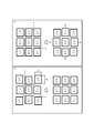
- FIG. 2 is used to explain local differences in substrate expansion and contraction when a planar substrate is bent. It is known that when a flat substrate is bent to form a curved surface, the elongation of the substrate increases in a region closer to the center of the curved surface.
- the setting method of the section 20 for forming the fine structure 2 will be examined.
- square-shaped division groups 20 arranged at equal intervals in the vertical and horizontal directions on the original plane are arranged at equal intervals in the vertical and horizontal directions on the surface of the substrate (silicon wafer 1).
- the partition groups 20 are arranged at unequal intervals in a distribution like barrel distortion in the imaging optical system.
- the square partition groups 20 are arranged in advance on the original flat substrate so as to have an inverse relationship to the barrel distortion. That is, the interval between the sections 20 is set so that the vicinity of the center is narrow and the periphery is wide.
- the partition group 20 is set on the silicon wafer 1 so that a predetermined arrangement (a state in which they are arranged at equal intervals in the vertical and horizontal directions) is obtained after the curved surface forming process is performed.
- FIG. 2 shows a case in which the sections 20 for forming the fine structure 2 are arranged in 3 ⁇ 3 in the vertical direction, but 4 ⁇ 4 in the vertical direction, 3 ⁇ 4 in the vertical direction, and so on. The same applies to other values.
- the groove pattern made of the photoresist can be transferred to the silicon oxide film or the silicon wafer substrate itself by using plasma etching or the like.
- an aluminum film or the like can be deposited on the surface of the microstructure 2 in order to improve optical performance such as reflectance.
- the third step shown in FIG. 1C is a step of thinning the silicon wafer 1 and is one of preparation steps for the curved surface processing.
- the thickness t1 of the silicon wafer 1 is as large as several hundreds of micrometers, it is not suitable for an etching process in a later process. That is, the initial thickness dimension t1 of the silicon wafer 1 is too thick for etching.
- the silicon wafer 1 is thinned by polishing or wet etching from the back surface thereof.
- the thickness dimension t3 of the silicon wafer 1 becomes thinner than the initial value t1 (t3 ⁇ t1).
- the thickness dimension t3 of the silicon wafer 1 after the thinning process is set to a thickness that can maintain rigidity in each section, for example, a thickness of about 100 ⁇ m.
- the 4th process shown in Drawing 1 (d) is a support substrate joining process, and is one of the preparation processes for curved surface formation processing. Since a silicon single crystal is a brittle material, even if it is thinned, if it is curved with a small curvature radius and a large displacement, it will be broken due to a buckling phenomenon or the like.
- the single crystal silicon in the gap 8 partitioning each section is removed by etching so that a large bending displacement can be absorbed by the gap 8 as a “groove”.
- the support substrate 3 made of a flexible material having excellent bendability is bonded to the back surface of the thinned silicon wafer 1, and the position of the microstructure 2 in each separated section is held.
- the support substrate 3 corresponds to a “first substrate”.
- the flexible material for example, nickel is used here, but is not limited thereto.
- Other materials may be used as long as they can be bent uniformly and smoothly by plastic deformation, can maintain the curved shape after plastic deformation, and have rigidity that does not easily deform by external force.
- a metal material rich in spreadability is suitable. It is difficult to maintain a deformed shape of resin and glass with high accuracy.
- resin or glass may be used as the material of the support substrate 3.
- the fifth step shown in FIG. 1 (e) is a gap forming step, which is one of preparation steps for the curved surface forming process.
- the silicon single crystal in the gap 8 is removed by plasma etching or the like.
- the thinned silicon wafer 1 is separated into a single crystal substrate 1A divided into a plurality of sections for each section.
- the separated single crystal substrate 1A corresponds to the “second substrate”.
- the sixth step shown in FIG. 1 (f) is a protective layer forming step.
- the surface of each microstructure 2 is covered with a protective layer 4.
- the thickness unevenness of the protective layer 4 affects the surface accuracy of the curved optical element to be completed. Therefore, the film thickness variation of the protective layer 4 needs to be suppressed to a desired accuracy, for example, 1 ⁇ 4 or less of the wavelength used as the optical element.
- the seventh step shown in FIG. 1 (g) is a curved surface forming step.
- the prepared planar optical element is sandwiched and pressed from both the upper and lower directions.
- the support substrate 3 is plastically deformed to conform to the three-dimensional curved surface shape of the mold.
- the curved surface forming process can also be called a pressurizing process.
- the eighth step shown in FIG. 1 (h) is the final step.
- the optical element 10 having a desired three-dimensional curved surface shape is completed. If the protective layer 4 does not adversely affect the optical properties, it may be left without being removed.
- the fine structure 2 is produced by applying the photolithography technique to the silicon wafer 1. For this reason, according to the present embodiment, it is possible to manufacture a curved optical element having a small size and high accuracy. Further, according to the present embodiment, a pattern with a high degree of freedom can be formed by changing the layout data of the photomask to be used.
- a plurality of small-area sections 20 are set on the surface of the single crystal silicon wafer 1, and the single crystal silicon in the gaps 8 of each section is removed, whereby a plurality of silicon wafers 1 are formed.
- the entire support substrate 3 supporting each single crystal substrate 1A is curved. Therefore, according to the present embodiment, a silicon single crystal which is a brittle material is used, and a curved optical element having a large area as a whole (see element diameter D1 in FIGS. 4 and 5) has a small curvature without causing crystal breakage. It can be formed into a three-dimensional curved surface having a large displacement with a radius.
- the support substrate 3 made of a flexible material can be plastically deformed along the shape of the molds 5 and 6, the surface accuracy of the entire curved optical element is increased. And the accuracy can be maintained.
- the second embodiment will be described with reference to FIG. Since this embodiment corresponds to a modification of the first embodiment, differences from the first embodiment will be mainly described.
- a case will be described in which the present invention is applied to a curved optical element 10A that requires electrical connection, such as a light receiving element, a light emitting element, or a MEMS optical element such as a micromirror or a microshutter.
- the light receiving element array, the light emitting element array, and the MEMS optical element array are array optical elements in which unit elements such as a light receiving element, a light emitting element, and a MEMS element are two-dimensionally arranged. In these array optical elements, it is necessary to electrically connect the unit elements. Therefore, in this embodiment, in the fine structure forming step (FIG. 2B), a unit element is formed as the fine structure 2, and each wiring layer 7 for electrically connecting the single crystal substrates 1A is provided. It is provided between the crystal substrate 1 ⁇ / b> A and the support substrate 3.
- FIG. 2 shows a method of manufacturing the curved optical element 10A according to this example.
- the wafer preparation step (FIG. 1A) which is the first step described in the first embodiment is omitted.
- the second step shown in FIG. 2 (b) is a fine structure forming step in which the fine structure 2 serving as a unit element is formed on the silicon wafer 1 in a predetermined arrangement.
- the third step shown in FIG. 2C is a step of thinning the silicon wafer 1 and is one of the preparation steps for the curved surface processing.
- the 3A process added by the present Example shown in FIG.2 (c2) is a wiring layer formation process in which the wiring layer 7 is formed in the back surface side of the silicon wafer 1 after a thinning process.
- Wiring layer 7 includes a wiring pattern for electrically connecting each single crystal substrate 1A.
- each single crystal substrate 1A is electrically connected to, for example, another single crystal substrate 1A to which each single crystal substrate 1A is to be connected, or a wiring pattern or an electrical element such as a capacitor (not shown). Means that.
- the conductor portion of the wiring layer 7 is formed as a copper foil, and the insulating base portion of the wiring layer 7 is formed of a resin such as polyimide or a rubber material such as silicone.
- the 4th process shown in Drawing 2 (d) is a support substrate joining process, and is one of the preparation processes for curved surface formation processing. In this step, the support substrate 3 is bonded to the back side of the wiring layer 7.
- the fifth step shown in FIG. 2 (e) is a gap forming step, which is one of preparation steps for the curved surface forming process.
- the gap portion 8 is formed by removing the single crystal silicon between the sections by etching.
- the single silicon wafer 1 is divided into single crystal substrates 1A along each section by the gap 8.
- the sixth step shown in FIG. 2 (f) is a protective layer forming step.
- the protective layer 4 is formed so as to cover each single crystal substrate 1A and each gap 8.
- the seventh step shown in FIG. 2 (g) is a curved surface forming step.
- a surface pressure is applied by sandwiching the planar optical element from both sides in the vertical direction by the convex mold 5 and the concave mold 6.
- the single-crystal substrate 1A and the wiring layer 7 divided into the support substrate 3 and the plurality of single-crystal substrates 1A are arranged in a predetermined curved surface shape (a three-dimensional curved surface having a non-developable surface). Shape) to form a curved surface.
- the eighth step shown in FIG. 2 (h) is the final step.
- the molds 5 and 6 are removed, and the protective layer 4 is removed if unnecessary. Thereby, it is possible to obtain an optical element 10A that can transmit and receive electrical signals and has a desired curved surface.
- the wiring layer 7 may be provided inside the supporting substrate 3 or on the back side of the supporting substrate 3 instead of the configuration in which the wiring layer 7 is provided between each single crystal substrate 1A and the supporting substrate 3. In that case, a through electrode for connecting each single crystal substrate 1 ⁇ / b> A and the wiring layer 7 is formed on the support substrate 3.
- This embodiment which is configured in this way, also has the same function and effect as the first embodiment. Further, in this embodiment, since the wiring layer 7 for electrically connecting each single crystal substrate 1A is provided, a unit requiring electrical connection, such as a light receiving element array, a light emitting element array, or a MEMS optical element array. A curved optical element 10A in which elements are arrayed can be obtained.
- the third embodiment will be described with reference to FIG.
- This embodiment relates to an improvement of the first embodiment.
- the base 6 as a “reinforcing member” is joined from the back surface of the support substrate 3 as shown in the cross-sectional view of FIG.
- the mechanical strength of the curved optical element 10B can be increased.
- the lower mold 6 used in the curved surface forming process is used as a pedestal.
- the mold 6 can be bonded to the back side of the support substrate 3 during the curved surface forming step or after the curved surface forming step.
- only the upper mold 5 is removed from the curved optical element in the above-described final step (FIG. 1 (h)).
- the protective layer 4 may be removed or left as it is.
- This embodiment which is configured in this way, also has the same function and effect as the first embodiment. Furthermore, since the base 6 is provided in this embodiment, the strength of the curved optical element 10B can be increased.
- the strength of the curved optical element 10B is increased and the reliability and usability are improved without complicating the manufacturing process. it can.
- a fourth embodiment will be described with reference to FIG. This embodiment relates to an improvement of the second embodiment. Similarly to the third embodiment, in this embodiment, the strength can be secured by joining the base 6 to the curved optical element 10C.
- this invention is not limited to the Example mentioned above.
- a person skilled in the art can make various additions and changes within the scope of the present invention.
- Various numerical values such as the size of the element, the formation density of the parallel grooves, the number of elements arranged, and the width of the gap are examples, and the present invention is not limited thereto.
- An appropriate numerical value may be set according to the use of the element based on the wavelength region to be used.
- the thinning process shown in FIGS. 1C and 2C may be omitted.
- 1 silicon wafer
- 1A single crystal substrate
- 2 fine structure
- 3 support substrate
- 4 protective layer
- 5 upper mold
- 6 lower mold
- 7 wiring layer
- 8 gap
- 10A, 10B, 10C curved surface optical element
Landscapes
- Physics & Mathematics (AREA)
- General Physics & Mathematics (AREA)
- Optics & Photonics (AREA)
- Micromachines (AREA)
Abstract
複数の単結晶基板を用い、全体として非可展面の曲面形状を有する曲面光学素子を提供する。単一の単結晶基板1の表面には、複数の所定区画が所定間隔で設定されている。各所定区画に所定の光学的構造2を形成する(b)。所定の光学的構造2を形成した単一の単結晶基板1の裏面側に第1基板3を接合する(d)。単一の単結晶基板1の表面から第1基板3に至る溝8を各所定区画間に形成することで、単一の単結晶基板1を所定区画ごとに分離して各第2基板1Aを形成する(e)。第1基板3および各第2基板1Aを法線方向から押圧する曲面形成処理を実施することにより、第1基板の一方の面を所定の曲面形状に形成する共に、各所定の光学的構造を結ぶ包絡面を所定の曲面形状に形成する(g)。
Description
本発明は、曲面光学素子およびその製造方法に関する。
表面に微細な光学的構造を有する曲面光学素子として代表的なものに、凹面回折格子がある。従来、ナノインプリントなどレプリカ技術で元の金型から複製品を作製する方法を除くと、曲面光学素子またはそのレプリカを作製するための金型を製造する方法は、主として以下の2つである。
一つの方法は、特許文献1に記載のように、曲面上をダイヤモンド工具で加工する機械加工方式である。他の一つの方法は、特許文献2に記載のように、曲面上に塗布したフォトレジストに対してレーザー光を照射する干渉露光方式である。従来は、上記いずれかの方法を用いて基板の曲面上を直接加工することで、所望の微細構造を形成する。
一方最近では、平面状の光学素子を曲げ加工して曲面化することで、曲面光学素子を製造する技術も開発されている(特許文献3~6)。このように、表面または表面近傍に微細構造を有する曲面光学素子を製作する方法は、曲面上に微細構造を直接加工または形成する方法と、微細構造を形成した平面素子を曲面化することによって曲面素子を得る方法とに大別される。
近年、反射防止膜や回折光学素子をはじめ、光学素子表面への微細構造の形成は、急速に重要性を増している。さらに、微細構造の小寸法化、形状の高精度化および多様化も求められている。
従来の平面光学素子では、半導体製造に用いるフォトリソグラフィ技術を応用することによって、微細構造の小寸法化、形状の高精度化および多様化に対応している。しかし、フォトリソグラフィに用いる露光装置は焦点深度が浅いため、平面上に形成する場合と同等レベルの高精細パターンを曲面上に形成することは非常に困難である。従って、曲面上での微細加工にフォトリソグラフィ技術を適用するのは難しい。
一方、上述した特許文献1に記載の機械加工方式では、加工精度が、使用するダイヤモンド工具の精度に制約されるため、形状の高精度化に対応できない。特許文献2に記載の干渉露光方式では、加工可能なパターンが単純な繰り返し周期構造のもの限られるため、形状の多様化に対応できない。
平面光学素子を曲げ加工することで曲面光学素子を得る方法では、フォトリソグラフィ技術を応用して、元になる平面光学素子を製作することができる。従って、平面光学素子上に微細構造を形成する段階では、精度および多様化の課題を解決できる。
ところで、フォトリソグラフィの利点を最大に引き出すためには、シリコンウェーハ基板を用いることが好ましい。しかし、シリコンウェーハを構成するシリコン単結晶は、展延性が乏しい脆性材料であるため、曲げ加工が非常に困難である。従って、特許文献3に記載の技術は、その適用範囲が狭い。つまり、小面積なシリコンウェーハであって、かつ中心部と周辺部の高低差の小さい小変位の曲面化についてのみ役立つ。
特許文献4に記載の技術では、素子全体を複数区画に分け、各区画を仕切る境界部で、積極的に結晶格子面の大きな滑りを伴う変形を起こさせることで、素子全体を折れ線状に疑似曲面化する。従って、この従来技術は、1軸の周りに曲面化した円筒面において、大面積かつ中心部と周辺部の高低差も比較的大きい曲面化を実現する。
ここで、円筒面や円錐面のような曲面は可展面と呼ばれる。可展面は、厚みの無視できる薄板を曲げて作る場合、元の平面状態から局所的な伸縮を伴うことなく容易に曲面化できる。これに対し、球面などの、より一般的な曲面は三次元曲面と呼ばれる。三次元曲面は、元の平面から局所的な伸縮を伴わずに曲面化することはできない。
特許文献4に記載の従来技術では、可展面である円筒にのみ対応しており、非可展面である三次元曲面の形成については全く考慮していない。平面光学素子を例えば球面化する場合を考えると、特許文献4における境界部の幅方向には、結晶格子面をずらす方向の応力だけでなく、引き裂く方向、または圧縮する方向の応力が働く。
このため中心部と周辺部での高低差が大きくなると、結晶格子面が上下にずれるだけでは吸収されず、境界部およびその周辺が、引っ張り、あるいは圧縮による座屈によって、変形または破断する。これにより、各区画の配列間隔や表面形状の制御ができなくなってしまうことが容易に予測される。
特許文献5に記載の従来技術では、シリコン単結晶の曲げ性を改善するために、シリコンの融点に近い高温下で曲面化する。従って、そのような極端環境下で生じる歪みや潰れあるいは変形が微細構造にとって問題となる場合や、高温で特性が変化してしまう材料が含まれている場合には、特許文献5に記載の従来技術を適用することはできない。
特許文献6に記載の従来技術では、シリコン基板上に形成された微細構造を、曲げ性に富む別材料から成る基板に転写した後で、その別材料の基板を曲面化する。反射型回折格子のように素子の材料を問わない場合は、この従来技術の利点を享受できる。反射型回折格子は、最終的に、素子表面にアルミニウムのような高反射膜が蒸着されれば、反射型回折格子としての光学性能を発揮するためである。
しかし、電気的動作を伴う受光素子アレイの場合や、さらに機械的動作も加わるMEMS(Micro Electro Mechanical Systems)素子などの場合は、基板自体が素子の機能発現に大きく関わっているため、特許文献6に記載の従来技術を適用することはできない。受光素子アレイやMEMS素子などの場合、素子の一部である表面形状のみを他の材料から形成したのでは、そもそも素子として機能しない。このように従来技術では、単結晶基板を用いて非可展面の曲面形状を有する曲面光学素子を提供することは困難であった。
本発明は上記課題に鑑みてなされたもので、その目的は、複数の単結晶基板を用い、全体として非可展面の曲面形状を有する曲面光学素子を提供することにある。
上記課題を解決すべく、本発明の一つの観点に従う曲面光学素子は、可撓性を有し、非可展面である所定の曲面形状に形成される第1基板と、単結晶基板からなる複数の第2基板であって、第1基板の一方の面に所定間隔離間して配置され、その表面側には所定の光学的構造がそれぞれ形成されている複数の第2基板と、を備え、各第2基板が有する所定の光学的構造を結ぶ包絡面は、所定の曲面形状を形成するようになっている。
各第2基板は、単一の単結晶基板から分離される基板として形成できる。
第1基板および単一の単結晶基板の初期形状は、それぞれ平板状であり、単一の単結晶基板の表面には、複数の所定区画が所定間隔で設定されており、各所定区画には、所定の光学的構造をそれぞれ形成し、各所定の光学的構造を形成した単一の単結晶基板の裏面側に第1基板の一方の面を接合し、単一の単結晶基板の表面から第1基板の一方の面に至る溝を各所定区画間にそれぞれ形成することで、単一の単結晶基板を所定区画ごとに分離して各第2基板を形成し、第1基板および各第2基板を法線方向から押圧する曲面形成処理を実施することにより、第1基板の一方の面を所定の曲面形状に形成する共に、各所定の光学的構造を結ぶ包絡面を所定の曲面形状に形成する、こともできる。
本発明によれば、可撓性を有し、非可展面である所定の曲面形状に形成される第1基板と、表面側に所定の光学的構造が形成された単結晶基板からなる複数の第2基板を用いることで、所定の曲面形状を有する光学素子を得ることができる。
以下、図面に基づいて、本発明の実施の形態を説明する。本実施形態では、以下に詳述する通り、(1)単一の単結晶基板(例えばシリコン基板等)上に所定間隔で所定の光学的構造としての微細構造を二次元配列し、(2)微細構造を二次元配列した単一の単結晶基板の裏面側に第1基板としての支持基板を接合し、(3)二次元配列した各微細構造の間を支持基板の表面に達するまでエッチングすることで、それぞれが微細構造を有する複数の第2基板としての単結晶基板を支持基板上に形成し、(4)各単結晶基板および支持基板を法線方向上下から押圧する曲面形成処理を実施することで、各単結晶基板の微細構造を結ぶ包絡面と前記支持基板とを、非可展面である所定の曲面形状に形成する。
これにより、本実施形態では、シリコンなどの単結晶基板を用いて製造した、表面または表面近傍に微細構造を有する平面光学素子を元にして、その微細構造に歪み、潰れ、変形を生じさせることなく、曲面光学素子を得ることができる。また本実施形態によれば、光学素子としての機能発現を損なわない環境下で、大面積かつ中心部と周辺部での高低差の大きい三次元曲面化を実施することができ、良好な性能の曲面光学素子を得ることができる。
さらに、本実施形態では、微細構造をそれぞれ有する単結晶基板の元となる単一の単結晶基板の裏面側に配線層を設け、各微細構造の間を配線層の表面に達するまでエッチングすることで、各単結晶基板を形成することもできる。これにより、電気信号の送受を要する素子なども製造することができる。
図1および図2を用いて第1実施例を説明する。図1は、第1実施例に係る曲面光学素子の製造方法を示す。本実施例では、曲面光学素子の例として、単位回折格子が縦横二次元に並んだ回折格子アレイを挙げる。
各単位回折格子は、例えば、外形が一辺3mmの正方形で、600本/mmの溝を平行に刻んだ平面回折格子である。本実施例では、単位回折格子を縦横に例えば3×3枚並べて、支持基板と一緒に曲面形成処理を施すことで、平面回折格子をアレイ化した疑似凹面回折格子を製造する。
図1(a)に示す第1工程は、ウェーハ準備工程である。基板準備工程と呼ぶこともできる。第1工程では、所定の厚み寸法t1を有するシリコンウェーハ1を用意する。シリコンウェーハ1は「単一の単結晶基板」の一例であり、後述のように「第2基板」としての単結晶基板1Aの元となる。
図1(b)に示す第2工程は、シリコンウェーハ1上に「所定の光学的構造」としての微細構造2を所定の配置で形成する微細構造形成工程である。まずシリコンウェーハ1上にフォトレジストを適切な膜厚t2で塗布した後、図外の露光装置を用いて、シリコンウェーハ1上に設定する各所定区画に平行溝のパターンからなる微細構造2を形成する。1つの所定区画の横寸法はw1、縦寸法はh1である。横寸法w1×縦寸法h1の所定区画は、縦n個×横m個並んで配設される。平行溝のパターンは、例えば、1mmあたり600本の浅い平行溝として形成される。
なお、幅寸法w1および縦寸法をそれぞれ3mm程度の同一値に設定してもよいし、異なる値に設定してもよい。平行溝の形成密度は600本/mmに限らず、1mmあたり600本未満でもよいし、1mmあたり600本を超えた数であってもよい。所定区画の配置は、例えば縦3個(n=3)、横3個(m=3)でもよいし、または2や4以上の値に設定してもよい。縦の数nと横の数mとが異なってもよい。なお、微細構造2間には、幅寸法w2の間隙部8が設けられる。幅寸法w2は、例えば10μm程度に設定することができる。
図2を用いて、平面状の基板を曲げる場合の基板伸縮の局所的相違を説明する。平面状の基板を曲げて曲面化する場合、基板の伸びは、曲面化の中心に近い領域ほど大きくなることが知られている。
ここで、微細構造2を形成するための区画20の設定方法について検討する。図2(a)の左側に示すように、元の平面上で縦横等間隔に配列した正方形状の区画群20を、平面上の基板(シリコンウェーハ1)の表面に縦横等間隔で配置する。この状態で曲面形成処理を実施すると、図2(a)の右側に示すように、区画群20は、結像光学系における樽型歪みのような分布で不等間隔に並ぶことになる。
そこで、本実施例では、図2(b)の左側に示すように、予め元の平面基板上で正方形の区画群20を樽型歪みと逆の関係になるように配列する。つまり、中央部付近が狭く、周囲が広くなるように、区画20間の間隔を設定する。この状態で曲面形成処理を実施すると、図2(b)の右側に示すように、区画分20は、垂直上方から見たときに等間隔に並ぶ。従って、本実施例では、曲面形成処理の実施後に所定の配列(縦横等間隔で配置される状態)が得られるように、シリコンウェーハ1上に区画群20を設定する。図2では説明の便宜上、微細構造2を形成するための区画20を縦3個×横3個に並べる場合を示したが、縦4個×横4個、縦3個×横4個のように、他の値の場合も同様である。
なお、微細構造2を形成する工程(図2(b))において、フォトレジストで作製された平行溝パターンにおいて、機械的強度や化学的強度、あるいは耐熱性が問題となる場合も考えられる。その場合には、さらにプラズマエッチング等を用いて、前記フォトレジストで作製された溝パターンをシリコン酸化膜やシリコンウェーハ基板自体に転写して用いることもできる。また、反射率など光学的性能を向上させるために、微細構造2の表面にアルミニウム膜等を蒸着することもできる。
図1(c)に示す第3工程は、シリコンウェーハ1を薄くする工程であり、曲面化処理のための準備工程の一つである。一般にシリコンウェーハ1の厚み寸法t1は数100μm程度と大きいため、後の工程でのエッチング処理時に適していない。つまり、シリコンウェーハ1の最初の厚み寸法t1のままでは、エッチングを施すには厚過ぎる。
そこで、第3工程では、シリコンウェーハ1を、その裏面から研磨またはウエットエッチングすることにより薄くする。この薄片化処理の後、シリコンウェーハ1の厚み寸法t3は、初期値t1よりも薄くなる(t3<t1)。薄片化処理後のシリコンウェーハ1の厚み寸法t3は、各区画で剛性が維持できる程度の厚み、例えば100μm程度の厚みに設定される。
図1(d)に示す第4工程は、支持基板接合工程であり、曲面形成処理のための準備工程の一つである。シリコン単結晶は脆性材料であるため、薄片化しても、小さな曲率半径で変位の大きい曲面化を施すと、座屈現象などにより破壊されてしまう。
そこで、後述の第5工程では、各区画を仕切る間隙部8の単結晶シリコンをエッチングにより除去し、大きな曲げ変位を「溝」としての間隙部8で吸収できるようにする。しかし、間隙部8の単結晶シリコンをエッチングにより除去すると、各区画は分離してしまい、各微細構造2の相互の位置関係が保てなくなってしまう。このため第4工程では、薄片化したシリコンウェーハ1の裏面に、曲げ性に優れる可撓性材料から成る支持基板3を接合して、分離された各区画の微細構造2の位置を保持する。支持基板3は「第1基板」に該当する。
可撓性材料としては、ここでは例えばニッケルを用いるが、これに限らない。塑性変形によって一様かつ滑らかに曲げることができ、塑性変形後の曲面形状がそのまま維持できると共に、外力で容易に変形しない剛性をもつものであれば、他の材料でも良い。一般的には展延性に富む金属材料が好適である。樹脂やガラスは変形させた形状を高精度に維持することが難しい。しかし、上記の条件を満たすのであれば、樹脂やガラスを支持基板3の材料として用いてもよい。
図1(e)に示す第5工程は、間隙形成工程であり、曲面形成処理のための準備工程の一つである。微細構造2の形成されたシリコンウェーハ1の裏面側に支持基板3を接合した後、プラズマエッチング等によって、間隙部8のシリコン単結晶を除去する。これにより、薄片化されたシリコンウェーハ1は、各区画ごとに、複数に分割された単結晶基板1Aに分離される。分離された単結晶基板1Aは「第2基板」に該当する。
図1(f)に示す第6工程は、保護層形成工程である。各微細構造2が曲面形成処理時の加圧により変形したり破損したりする恐れがある場合、各微細構造2の表面を保護層4で覆う。
但し、保護層4の厚みムラは、でき上がる曲面光学素子の面精度に影響する。従って、保護層4の膜厚変動は所望の精度に、例えば光学素子として使用する波長の1/4等以下に抑える必要がある。以上の第1工程~第6工程により、表面に微細構造を有する曲面光学素子を作製する元になる平面光学素子が準備される。
図1(g)に示す第7工程は、曲面形成工程である。曲面光学素子として仕上げる所望の三次元曲面形状に合わせた凸面金型5および凹面金型6を用いて、準備した平面光学素子を上下両方向から挟みこんで加圧する。これにより、支持基板3を塑性変形させて、金型の持つ三次元曲面形状に沿わせる。曲面形成工程は加圧工程と呼ぶこともできる。
図1(h)に示す第8工程は、最終工程である。金型5,6を取り外し、さらに保護層4を除去することにより、所望の三次元曲面形状を有する光学素子10が完成する。なお、保護層4が光学的に悪影響を及ぼさない場合には、除去せずに残してもよい。
本実施例では、凹面状の光学素子の製造例を示したが、凸面状の光学素子の場合には、凸面金型5および凹面金型6の関係を入れ替えればよい。
このように構成される本実施例によれば、シリコンウェーハ1に対しフォトリソグラフィ技術を応用して微細構造2を作製する。このため、本実施例によれば、小寸法かつ高精度な曲面光学素子の製造が可能である。また、本実施例によれば、使用するフォトマスクのレイアウトデータを変更することで、自由度の高いパターンを形成できる。
また、本実施例によれば、単結晶のシリコンウェーハ1の表面に複数の小面積の区画20を設定し、各区画の間隙部8の単結晶シリコンを除去することでシリコンウェーハ1を複数の単結晶基板1Aに分離し、その後に各単結晶基板1Aを支える支持基板3の全体を曲面化する。従って、本実施例によれば、脆性材料であるシリコン単結晶も用いて、全体として大面積の曲面光学素子(図4,5の素子直径D1参照)を、結晶破壊をきたすことなく、小さな曲率半径で変位の大きい三次元曲面に形成できる。
本実施例によれば、図1(g)に示す曲面形成工程では、支持基板3および各単結晶基板1Aに上下方向から機械的に圧力をかけるだけであり、例えば200℃以上などの高温環境は不要である。従って、本実施例によれば、微細構造2に高温が作用して精度が低下するなどの問題は生じない。
また、本実施例では、可撓性材料から成る支持基板3を金型5,6の形状に忠実に沿って塑性変形させることができるため、曲面光学素子全体としての面の精度を高くすることができ、かつその精度を維持することができる。
図3を用いて第2実施例を説明する。本実施例は第1実施例の変形例に相当するため、第1実施例との相違を中心に説明する。本実施例では、受光素子、発光素子、あるいはマイクロミラーやマイクロシャッタなどのMEMS光学素子などの、電気的接続を必要とする曲面光学素子10Aに適用する場合を説明する。
受光素子アレイ、発光素子アレイ、MEMS光学素子アレイは、受光素子、発光素子、MEMS素子といった単位素子を二次元配列したアレイ光学素子である。これらアレイ光学素子では、各単位素子間を電気的に接続する必要が発生する。そこで、本実施例では、微細構造形成工程(図2(b))において、微細構造2として単位素子を形成し、さらに、単結晶基板1A間を電気的に接続するための配線層7各単結晶基板1Aと支持基板3の間に設ける。
図2は、本実施例による曲面光学素子10Aの製造方法を示す。図2では、第1実施例で述べた第1工程であるウェーハ準備工程(図1(a))を省略している。
図2(b)に示す第2工程は、シリコンウェーハ1上に単位素子となる微細構造2を所定の配置で形成する微細構造形成工程である。
図2(c)に示す第3工程は、シリコンウェーハ1を薄くする工程であり、曲面化処理のための準備工程の一つである。
図2(c2)に示す本実施例で追加された第3A工程は、薄片化処理後のシリコンウェーハ1の裏面側に配線層7を形成する配線層形成工程である。配線層7は、各単結晶基板1Aを電気的に接続するための配線パターンを含む。
なお、各単結晶基板1Aを電気的に接続するとは、例えば、各単結晶基板1Aが接続されるべき他の単結晶基板1A、または配線パターン、または図外のコンデンサなどの電気素子に接続することを意味する。
配線層7は、後述の曲面形成工程(図2(g))において支持基板3とともに曲面化されるため、曲げ性の良好な材質で構成されている必要がある。そこで例えば、配線層7のうち導体部分は銅箔として形成し、配線層7のうち絶縁基材部はポリイミドなどの樹脂、またはシリコーンなどのゴム素材から形成する。
図2(d)に示す第4工程は、支持基板接合工程であり、曲面形成処理のための準備工程の一つである。この工程では、配線層7の裏面側に支持基板3を接合する。
図2(e)に示す第5工程は、間隙形成工程であり、曲面形成処理のための準備工程の一つである。この工程では、各区画の間の単結晶シリコンをエッチングで除去することで、間隙部8を形成する。間隙部8により単一のシリコンウェーハ1は各区画に沿った単結晶基板1Aに分割される。
図2(f)に示す第6工程は、保護層形成工程である。この工程では、各単結晶基板1Aおよび各間隙部8を覆うようにして保護層4を形成する。
図2(g)に示す第7工程は、曲面形成工程である。この工程では、凸面金型5および凹面金型6により、平面光学素子を上下方向両側から挟みこんで面圧をかける。これにより、支持基板3と複数に分割された各単結晶基板1Aと配線層7とを、各単結晶基板1Aの表面側の包絡面が所定の曲面形状(非可展面である三次元曲面形状)を成すように一体として曲面化する。
図2(h)に示す第8工程は、最終工程である。本工程では、金型5,6を取り外すと共に、不要な場合には保護層4を除去する。これにより、電気信号の送受が可能で、かつ所望の曲面を有する光学素子10Aを得ることができる。
なお、各単結晶基板1Aと支持基板3の間に配線層7を設ける構成に代えて、支持基板3の内部または支持基板3の裏側に配線層7を設ける構成としてもよい。その場合は、各単結晶基板1Aと配線層7とを接続するための貫通電極を支持基板3に形成する。
このように構成される本実施例も第1実施例と同様の作用効果を奏する。さらに本実施例では、各単結晶基板1Aを電気的接続するための配線層7を設けるため、受光素子アレイ、発光素子アレイ、MEMS光学素子アレイのような、電気的な接続を必要とする単位素子をアレイ化した曲面光学素子10Aを得ることができる。
図4を用いて第3実施例を説明する。本実施例は第1実施例の改良に関する。曲面光学素子10Bの使用時に、大きな外力が加わる可能性のある場合は、図4の断面図に示すように、支持基板3の裏面から「補強部材」としての台座6を接合する。台座6を設けることで、曲面光学素子10Bの機械的強度を高めることができる。
本実施例では、曲面形成工程で使用した下側の金型6を台座として利用する。曲面形成工程の最中に、あるいは曲面形成工程の終了後に、金型6を支持基板3の裏面側に接合することができる。この場合、上述した最終工程(図1(h))では、上側の金型5のみを曲面光学素子から取り外す。保護層4は除去してもよいし、そのまま残してもよい。
このように構成される本実施例も第1実施例と同様の作用効果を奏する。さらに本実施例では、台座6を設けるため、曲面光学素子10Bの強度を高めることができる。
また本実施例では、曲面形成工程で用いた下側の金型6を台座6として利用するため、製造工程を複雑化せずに、曲面光学素子10Bの強度を高め、信頼性や使い勝手を向上できる。
図5を用いて第4実施例を説明する。本実施例は第2実施例の改良に関する。本実施例も第3実施例で述べたと同様に、曲面光学素子10Cに台座6を接合することで、強度を確保することができる。
なお、本発明は、上述した実施例に限定されない。当業者であれば、本発明の範囲内で、種々の追加や変更等を行うことができる。素子の大きさや平行溝の形成密度、素子の配置個数、間隙部の幅寸法などの各種の数値は一例であり、それらに限定しない。使用する波長領域などに基づき、素子の用途に応じた適切な数値に設定すればよい。
また、シリコンウェーハ1の厚さ寸法が十分薄い場合は、図1(c)、図2(c)に示す薄片化処理を省略してもよい。
1:シリコンウェーハ、1A:単結晶基板、2:微細構造、3:支持基板、4:保護層、5:上側の金型、6:下側の金型、7:配線層、8:間隙部、10,10A,10B,10C:曲面光学素子
Claims (12)
- 可撓性を有し、非可展面である所定の曲面形状に形成される第1基板と、
単結晶基板からなる複数の第2基板であって、前記第1基板の一方の面に所定間隔離間して配置され、その表面側には所定の光学的構造がそれぞれ形成されている複数の第2基板と、
を備え、
前記各第2基板が有する前記所定の光学的構造を結ぶ包絡面は、前記所定の曲面形状を形成する、
曲面光学素子。
- 前記各第2基板は、単一の単結晶基板から分離される基板として形成される、
請求項1に記載の曲面光学素子。
- 前記第1基板および前記単一の単結晶基板の初期形状は、それぞれ平板状であり、
前記単一の単結晶基板の表面には、複数の所定区画が所定間隔で設定されており、
前記各所定区画には、前記所定の光学的構造をそれぞれ形成し、
前記各所定の光学的構造を形成した前記単一の単結晶基板の裏面側に前記第1基板の前記一方の面を接合し、
前記単一の単結晶基板の表面から前記第1基板の前記一方の面に至る溝を前記各所定区画間にそれぞれ形成することで、前記単一の単結晶基板を前記所定区画ごとに分離して前記各第2基板を形成し、
前記第1基板および前記各第2基板を法線方向から押圧する曲面形成処理を実施することにより、前記第1基板の前記一方の面を前記所定の曲面形状に形成する共に、前記各所定の光学的構造を結ぶ包絡面を前記所定の曲面形状に形成する、
請求項2に記載の曲面光学素子。
- 前記曲面形成処理の実施により生じる基板伸縮の局所的相違を考慮し、前記曲面化処理の実施後に前記各第2基板が所定の配列を形成するように、前記各所定区画の配置が設定されている、
請求項3に記載の曲面光学素子。
- 所定の光学的構造は、回折格子である、
請求項1~4のいずれかに記載の曲面光学素子。
- 前記第1基板と前記各第2基板の間には、前記各第2基板を電気的に接続するための配線層が設けられている、
請求項1~4のいずれかに記載の曲面光学素子。
- 前記各所定の光学的構造を形成した前記単一の単結晶基板の裏面側に前記第1基板の前記一方の面を接合する前に、前記単一の単結晶基板の裏面側に配線層を接合し、
前記配線層の裏面側に前記第1基板の前記一方の面を接合し、
前記単一の単結晶基板の表面から前記配線層の表面に至る溝を前記各所定区画間にそれぞれ形成することで、前記単一の単結晶基板を前記所定区画ごとに分離して前記各第2基板を形成し、
前記第1基板と前記各第2基板および前記配線層を法線方向から押圧する曲面形成処理を実施することにより、前記第1基板の前記一方の面および前記配線層の表面を前記所定の曲面形状に形成する共に、前記各所定の光学的構造を結ぶ包絡面を前記所定の曲面形状に形成する、
請求項2または請求項4のいずれかに記載の曲面光学素子。
- 前記曲面形成処理のために前記第1基板の裏面側に接合される部材を、前記曲面形成処理の後も前記第1基板の裏面側に接合させることで補強部材として使用する、
請求項3または請求項7のいずれかに記載の曲面光学素子。
- 前記所定の光学的構造は、受光素子アレイ、発光素子アレイ、MEMS光学素子アレイ、のいずれか一つを構成するための構造である、
請求項7に記載の曲面光学素子。
- 曲面光学素子を製造する方法であって、
平板状に形成された単一の単結晶基板の表面に所定間隔で形成されている複数の所定区画に、所定の光学的構造を形成する工程と、
前記単一の単結晶基板を裏面側から削って所定の厚さに形成する工程と、
前記単一の単結晶基板の裏面側に配線層を接合する工程と、
前記配線層の裏面側に、可撓性を有する平板状の第1基板の一方の面を接合する工程と、
前記単一の単結晶基板の表面から前記配線層の表面に至る溝を前記各所定区画間にそれぞれ形成することで、前記単一の単結晶基板を前記所定区画ごとに分離して複数の第2基板を形成する工程と、
前記第1基板と前記各第2基板および前記配線層を上下の型部材を用いて挟み込むことで法線方向から押圧する曲面形成処理を実施することにより、前記第1基板の前記一方の面および前記配線層の表面を所定の曲面形状に形成する共に、前記各所定の光学的構造を結ぶ包絡面を前記所定の曲面形状に形成する工程と、
を実行する曲面光学素子の製造方法。
- 前記曲面形成処理の実施により生じる基板伸縮の局所的相違を考慮し、前記曲面化処理の実施後に前記各第2基板が所定の配列を形成するように、前記各所定区画の配置が設定されている、
請求項10に記載の曲面光学素子の製造方法。
- 曲面光学素子を製造する方法であって、
平板状に形成された単一の単結晶基板の表面に所定間隔で形成されている複数の所定区画に、所定の光学的構造を形成する工程と、
前記単一の単結晶基板を裏面側から削って所定の厚さに形成する工程と、
前記単一の単結晶基板の裏面側に、可撓性を有する平板状の第1基板の一方の面を接合する工程と、
前記単一の単結晶基板の表面から前記第1基板の一方の面に至る溝を前記各所定区画間にそれぞれ形成することで、前記単一の単結晶基板を前記所定区画ごとに分離して複数の第2基板を形成する工程と、
前記第1基板および前記各第2基板を上下の型部材を用いて挟み込むことで法線方向から押圧する曲面形成処理を実施することにより、前記第1基板の前記一方の面を所定の曲面形状に形成する共に、前記各所定の光学的構造を結ぶ包絡面を前記所定の曲面形状に形成する工程と、
を実行する曲面光学素子の製造方法。
Priority Applications (1)
| Application Number | Priority Date | Filing Date | Title |
|---|---|---|---|
| PCT/JP2015/050766 WO2016113856A1 (ja) | 2015-01-14 | 2015-01-14 | 曲面光学素子およびその製造方法 |
Applications Claiming Priority (1)
| Application Number | Priority Date | Filing Date | Title |
|---|---|---|---|
| PCT/JP2015/050766 WO2016113856A1 (ja) | 2015-01-14 | 2015-01-14 | 曲面光学素子およびその製造方法 |
Publications (1)
| Publication Number | Publication Date |
|---|---|
| WO2016113856A1 true WO2016113856A1 (ja) | 2016-07-21 |
Family
ID=56405420
Family Applications (1)
| Application Number | Title | Priority Date | Filing Date |
|---|---|---|---|
| PCT/JP2015/050766 Ceased WO2016113856A1 (ja) | 2015-01-14 | 2015-01-14 | 曲面光学素子およびその製造方法 |
Country Status (1)
| Country | Link |
|---|---|
| WO (1) | WO2016113856A1 (ja) |
Citations (6)
| Publication number | Priority date | Publication date | Assignee | Title |
|---|---|---|---|---|
| JP2010079174A (ja) * | 2008-09-29 | 2010-04-08 | Casio Computer Co Ltd | 電気機器 |
| JP2012013530A (ja) * | 2010-06-30 | 2012-01-19 | Fujifilm Corp | 回折格子及びその製造方法、並びに放射線撮影装置 |
| JP2012022239A (ja) * | 2010-07-16 | 2012-02-02 | Fujifilm Corp | 回折格子及びその製造方法、放射線撮影装置 |
| JP2013198661A (ja) * | 2012-03-26 | 2013-10-03 | Konica Minolta Inc | 格子および格子の製造方法ならびに格子ユニットおよび格子ユニットの製造方法 |
| WO2014034033A1 (ja) * | 2012-09-03 | 2014-03-06 | コニカミノルタ株式会社 | 回折格子および回折格子の製造方法、格子ユニットならびにx線撮像装置 |
| JP2014182301A (ja) * | 2013-03-19 | 2014-09-29 | Hitachi High-Technologies Corp | 曲面回折格子及びその製造方法、並びに光学装置 |
-
2015
- 2015-01-14 WO PCT/JP2015/050766 patent/WO2016113856A1/ja not_active Ceased
Patent Citations (6)
| Publication number | Priority date | Publication date | Assignee | Title |
|---|---|---|---|---|
| JP2010079174A (ja) * | 2008-09-29 | 2010-04-08 | Casio Computer Co Ltd | 電気機器 |
| JP2012013530A (ja) * | 2010-06-30 | 2012-01-19 | Fujifilm Corp | 回折格子及びその製造方法、並びに放射線撮影装置 |
| JP2012022239A (ja) * | 2010-07-16 | 2012-02-02 | Fujifilm Corp | 回折格子及びその製造方法、放射線撮影装置 |
| JP2013198661A (ja) * | 2012-03-26 | 2013-10-03 | Konica Minolta Inc | 格子および格子の製造方法ならびに格子ユニットおよび格子ユニットの製造方法 |
| WO2014034033A1 (ja) * | 2012-09-03 | 2014-03-06 | コニカミノルタ株式会社 | 回折格子および回折格子の製造方法、格子ユニットならびにx線撮像装置 |
| JP2014182301A (ja) * | 2013-03-19 | 2014-09-29 | Hitachi High-Technologies Corp | 曲面回折格子及びその製造方法、並びに光学装置 |
Similar Documents
| Publication | Publication Date | Title |
|---|---|---|
| CN106716639B (zh) | 使用张力的图像传感器弯曲 | |
| JP4347654B2 (ja) | 可変形状反射鏡及びその製造方法 | |
| CN101606086B (zh) | 用于制备可调透镜的方法 | |
| JP6029502B2 (ja) | 曲面回折格子の製造方法 | |
| TWI430390B (zh) | 減少疊對未對準之直接接合方法 | |
| US20100202071A1 (en) | Deformable mirror | |
| JP2011524084A (ja) | 分子接合を開始する方法 | |
| US8743449B2 (en) | Method and apparatus for providing high-fill-factor micromirror/micromirror arrays with surface mounting capability | |
| JP2001284567A (ja) | オプト・エレクトロニク撮像装置用焦点面および検出器、製造方法およびオプト・エレクトロニク撮像装置 | |
| TW201701450A (zh) | 在具有徑向變化之曲度的模具中彎折半導體晶片 | |
| US20130270662A1 (en) | Image sensor of curved surface | |
| JP2012530370A (ja) | 分子結合による結合方法 | |
| EP2240805B1 (en) | Membrane suspended optical elements, and associated methods | |
| WO2012126752A1 (en) | Apparatus and a method for direct wafer bonding, minimizing local deformation | |
| US8674460B2 (en) | Mechanical isolation for MEMS electrical contacts | |
| WO2016113856A1 (ja) | 曲面光学素子およびその製造方法 | |
| CN113023661B (zh) | 一种微镜及制作方法 | |
| KR100888080B1 (ko) | 마이크로미러 어레이 제작 방법 | |
| US10437005B2 (en) | Techniques for reducing distortion of optical beam shaping elements | |
| US9676609B2 (en) | Integrated MEMS device | |
| JP2007101649A (ja) | 光学レンズ,および,光学レンズの製造方法 | |
| JP5935396B2 (ja) | Mems素子及びmems素子の製造方法 | |
| US20030197176A1 (en) | Silicon on insulator standoff and method for manufacture thereof | |
| Bifano et al. | Megapixel wavefront correctors | |
| US20250136435A1 (en) | Stretchable electrical interconnect, flexible electronic system, and fabrication method thereof |
Legal Events
| Date | Code | Title | Description |
|---|---|---|---|
| 121 | Ep: the epo has been informed by wipo that ep was designated in this application |
Ref document number: 15877811 Country of ref document: EP Kind code of ref document: A1 |
|
| NENP | Non-entry into the national phase |
Ref country code: DE |
|
| 122 | Ep: pct application non-entry in european phase |
Ref document number: 15877811 Country of ref document: EP Kind code of ref document: A1 |
|
| NENP | Non-entry into the national phase |
Ref country code: JP |