WO2016104230A1 - 光電変換素子およびそれを用いた光電変換装置 - Google Patents
光電変換素子およびそれを用いた光電変換装置 Download PDFInfo
- Publication number
- WO2016104230A1 WO2016104230A1 PCT/JP2015/084987 JP2015084987W WO2016104230A1 WO 2016104230 A1 WO2016104230 A1 WO 2016104230A1 JP 2015084987 W JP2015084987 W JP 2015084987W WO 2016104230 A1 WO2016104230 A1 WO 2016104230A1
- Authority
- WO
- WIPO (PCT)
- Prior art keywords
- photoelectric conversion
- layer
- electrode layer
- conversion element
- power generation
- Prior art date
- Legal status (The legal status is an assumption and is not a legal conclusion. Google has not performed a legal analysis and makes no representation as to the accuracy of the status listed.)
- Ceased
Links
Images



Classifications
-
- H—ELECTRICITY
- H10—SEMICONDUCTOR DEVICES; ELECTRIC SOLID-STATE DEVICES NOT OTHERWISE PROVIDED FOR
- H10F—INORGANIC SEMICONDUCTOR DEVICES SENSITIVE TO INFRARED RADIATION, LIGHT, ELECTROMAGNETIC RADIATION OF SHORTER WAVELENGTH OR CORPUSCULAR RADIATION
- H10F10/00—Individual photovoltaic cells, e.g. solar cells
- H10F10/10—Individual photovoltaic cells, e.g. solar cells having potential barriers
- H10F10/16—Photovoltaic cells having only PN heterojunction potential barriers
- H10F10/167—Photovoltaic cells having only PN heterojunction potential barriers comprising Group I-III-VI materials, e.g. CdS/CuInSe2 [CIS] heterojunction photovoltaic cells
-
- H—ELECTRICITY
- H10—SEMICONDUCTOR DEVICES; ELECTRIC SOLID-STATE DEVICES NOT OTHERWISE PROVIDED FOR
- H10F—INORGANIC SEMICONDUCTOR DEVICES SENSITIVE TO INFRARED RADIATION, LIGHT, ELECTROMAGNETIC RADIATION OF SHORTER WAVELENGTH OR CORPUSCULAR RADIATION
- H10F77/00—Constructional details of devices covered by this subclass
- H10F77/20—Electrodes
-
- Y—GENERAL TAGGING OF NEW TECHNOLOGICAL DEVELOPMENTS; GENERAL TAGGING OF CROSS-SECTIONAL TECHNOLOGIES SPANNING OVER SEVERAL SECTIONS OF THE IPC; TECHNICAL SUBJECTS COVERED BY FORMER USPC CROSS-REFERENCE ART COLLECTIONS [XRACs] AND DIGESTS
- Y02—TECHNOLOGIES OR APPLICATIONS FOR MITIGATION OR ADAPTATION AGAINST CLIMATE CHANGE
- Y02E—REDUCTION OF GREENHOUSE GAS [GHG] EMISSIONS, RELATED TO ENERGY GENERATION, TRANSMISSION OR DISTRIBUTION
- Y02E10/00—Energy generation through renewable energy sources
- Y02E10/50—Photovoltaic [PV] energy
- Y02E10/541—CuInSe2 material PV cells
Definitions
- the present invention relates to a photoelectric conversion element having good characteristics and a photoelectric conversion device that is used by electrically connecting them.
- a photoelectric conversion device As a photoelectric conversion device, a plurality of photoelectric conversion elements including a substrate, a first electrode layer, a power generation layer, and a second electrode layer are provided, and the edges of adjacent photoelectric conversion elements are overlapped with each other by soldering or the like. What is connected to each other is known (see, for example, Patent Document 1). In this device, a practical voltage can be obtained by electrically connecting a plurality of photoelectric conversion elements.
- the photoelectric conversion element used for such a photoelectric conversion apparatus has the structure normally shown to Fig.7 (a), and each layer including the electric power generation layer 3 is formed very thinly. Therefore, as shown in FIG. 7B, if the end portion of the power generation layer 3 is missing, the second electrode layer 4 is easily bent in the direction of the white arrow, and the second electrode layer 4 becomes the first electrode layer 2. Contact may cause a short circuit of the photoelectric conversion element. In addition, during or after the production of the photoelectric conversion element, the photoelectric conversion element may cause a short circuit due to the conductive dust adhering across the first electrode layer 2 and the second electrode layer 4. If even one photoelectric conversion element that has caused a short circuit is provided, the voltage of the photoelectric conversion device will decrease as a whole, and the occurrence of a short circuit in the photoelectric conversion device is a major problem for the photoelectric conversion device.
- the present invention has been made in view of such circumstances, and a photoelectric conversion element that can effectively prevent short-circuiting caused by chipping or fine conductive dust adhering to the end of the power generation layer and photoelectric conversion using the photoelectric conversion element
- the purpose is to provide a device.
- the present invention is a substantially plate-like photoelectric conversion element having at least a substrate, a first electrode layer, a power generation layer, and a second electrode layer in this order, wherein the second electrode layer
- the photoelectric conversion element formed so that the side surface is located on the inner side of the side surface position of the power generation layer over the entire circumference is a first gist.
- the present invention is a photoelectric conversion device comprising a plurality of photoelectric conversion elements, wherein adjacent edges of the photoelectric conversion elements are overlapped and electrically connected, and each of the photoelectric conversion elements is at least a substrate and
- the first electrode layer, the power generation layer, and the second electrode layer have a substantially plate shape in this order, and the side surface of the second electrode layer is located inside the side surface position of the power generation layer over the entire circumference.
- the photoelectric conversion device which is the photoelectric conversion element of the first aspect formed as described above is defined as a second aspect.
- the present inventors have made various studies on a method for effectively preventing a short circuit of a photoelectric conversion element that causes a voltage drop. As a result, the inventors have found that an excellent short-circuit prevention effect can be obtained by devising the side surface portion of the photoelectric conversion element in which each layer is laminated, and have arrived at the present invention.
- the term “substantially plate-like” means that the whole plate-like material may be seen on the visual level. Therefore, it is not necessary for the whole to have a uniform thickness as long as it is within the plate-like concept when viewed as a whole.
- the photoelectric conversion element of the present invention is a substantially plate-like photoelectric conversion element having at least a substrate, a first electrode layer, a power generation layer, and a second electrode layer in this order.
- the side surface is formed so as to be located inside the side surface position of the power generation layer over the entire circumference. For this reason, even if chipping occurs at the end portion of the power generation layer, there is hardly a space for the end portion of the second electrode layer to bend toward the first electrode layer side, and the second electrode layer and the first electrode layer Contact is effectively prevented. Therefore, the photoelectric conversion element of the present invention is effectively prevented from being short-circuited.
- the photoelectric conversion element of the present invention is formed so that the shortest distance between the side surface of the first electrode layer and the side surface of the second electrode layer is longer, so that conductive dust is generated during the manufacture of the photoelectric conversion element. Even if it occurs, there is a low possibility that the conductive dust adheres so as to straddle the first electrode layer and the second electrode layer, and it is not easily short-circuited.
- the side surface of the power generation layer is formed so as to be located inside the side surface position of the first electrode layer over the entire circumference, the shortest distance from the side surface of the first electrode layer to the side surface of the second electrode layer. Can be further increased, and therefore a short circuit of the photoelectric conversion element is less likely to occur.
- the side surface of the first electrode layer, the side surface of the power generation layer, and the side surface of the second electrode layer are covered with the insulating coating material over the entire circumference, an impact is applied to the photoelectric conversion element from the outside. Even if it is a case, since it can prevent reliably that a 1st electrode layer and a 2nd electrode layer contact, a short circuit of a photoelectric conversion element becomes much less likely to occur.
- an insulating covering material that covers the entire circumference of the side surface if an insulating tape containing polyimide is used, the entire circumference of the side surface can be covered with a simple operation that is simply affixed. In addition, there is no damage due to an increase in extra steps when covering the entire side surface. Moreover, since the insulating tape containing polyimide is excellent in workability, even if the side shape of the photoelectric conversion element is complicated, it can be accurately handled, and the dimensional accuracy is excellent. Furthermore, since the insulating tape containing polyimide has sufficient heat resistance, it has sufficient resistance to thermal shock when incorporating a photoelectric conversion element into a photoelectric conversion device, and the shape as an insulating coating material may be impaired. Absent.
- an insulating coating material covering the entire circumference of the side surface is made of a thermoplastic resin composition containing at least one of an ethylene vinyl acetate copolymer resin and a urethane resin
- the composition is widely used as a sealing material for sealing, the same kind of composition as the sealing material is used as the insulating coating material, thereby increasing the affinity between the sealing material and the insulating coating material.
- a photoelectric conversion device with higher product reliability can be obtained.
- Adjacent photoelectric conversion elements can be fixed in a state where insulation is maintained.
- Such a photoelectric conversion device is more excellent in product reliability because it is resistant to mechanical impact such as bending.
- an insulating coating material covering the entire circumference of the side surface is formed of an inorganic oxide containing at least one selected from the group consisting of SiOx, AlOx, MgOx, and ZrOx.
- photoelectric conversion is performed.
- the durability against changes in the external environment such as humidity and temperature of the element can be enhanced. For this reason, the photoelectric conversion apparatus using such a photoelectric conversion element is more excellent in product reliability.
- the photoelectric conversion device includes a plurality of photoelectric conversion elements, and the adjacent edges of the photoelectric conversion elements are overlapped and electrically connected to each other, and each of the photoelectric conversion elements includes at least a substrate and a first electrode.
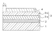
- FIG. 1 is a cross-sectional view schematically showing a photoelectric conversion element obtained by an embodiment of the present invention.
- This photoelectric conversion element is a CIGS solar cell in which a substrate 1, a first electrode layer 2, a power generation layer 3 composed of a light absorption layer 3a and a buffer layer 3b, and a second electrode layer 4 are laminated in this order. 2, the side surface of the second electrode layer 4 is formed so as to be located on the inner side by a length L 1 from the position of the side surface of the power generation layer 3 (light absorption layer 3 a and buffer layer 3 b) over the entire circumference. .
- this CIGS solar cell When this CIGS solar cell is irradiated with light from the second electrode layer 4 side, a pn junction is formed at the interface between the light absorption layer 3a and the buffer layer 3b, so that a current can be generated. It has become. In the case where a pn junction can be formed in the light absorption layer 3a, the buffer layer 3b is not necessarily required.
- this CIGS solar cell is demonstrated in detail.
- each part is shown typically and is different from an actual thickness, size, etc. (the same applies to the following figures).
- the side surface of a layer is “inside” the side surface position of the layer. It means that it is located on the center side of the photoelectric conversion element from the arrangement of the side surface of the layer.
- the first electrode layer 2 is formed.
- the light absorption layer 3a (thickness 2000nm) which consists of a compound semiconductor of chalcopyrite type crystal structure which has four elements of Cu, In, Ga, and Se, CdS layer (thickness 50nm,
- the side position is not limited to this.
- the L 1 is preferably 5 to 1000 ⁇ m. That is, when L 1 is less than 5 ⁇ m, when the dust of 0.1 to 5 ⁇ m present in a typical clean room (ISO 14644) is conductive, this dust becomes the first electrode layer 2 and the second electrode layer. This is because there is a possibility that a short circuit may occur due to adhesion across 4.
- stainless steel foil is used as the board
- SUS stainless steel foil
- substrate 1 when manufacturing the said CIGS photovoltaic cell by a roll to roll system or a stepping roll system, it is suitable for the said board
- the “long shape” means that the length in the length direction is 10 times or more of the length in the width direction, and more preferably 30 times or more.
- substrate 1 is 50 micrometers, you may use the board
- the thickness of the substrate 1 is preferably in the range of 30 ⁇ m to 200 ⁇ m, more preferably in the range of 50 ⁇ m to 100 ⁇ m. That is, if the thickness is too thick, the flexibility of the CIGS solar cell is lost, and there is a risk that the stress applied when it is bent increases and damages its internal structure. Conversely, if it is too thin, the CIGS solar cell This is because the substrate 1 is buckled and the product defect rate of the CIGS solar cells tends to increase.
- molybdenum (Mo) is used as the material for forming the first electrode layer 2, but W, Cr, Ti, or the like can be used in addition to that.
- the first electrode layer 2 may not be a single layer but a multilayer. Further, the thickness (in the case of multiple layers, the total thickness of each layer) is preferably 50 nm or more and 1000 nm or less.
- the thickness of the light absorption layer 3a formed on the said 1st electrode layer 2 is 2000 nm, you may form in thickness other than this.
- the thickness of the light absorption layer 3a is preferably in the range of 1.0 ⁇ m to 3.0 ⁇ m, and more preferably in the range of 1.5 ⁇ m to 2.5 ⁇ m. If the thickness is too thin, the amount of light absorption decreases and the performance of the CIGS solar cell tends to be reduced. Conversely, if the thickness is too thick, the time required for forming the light absorption layer 3a increases, resulting in increased productivity. This is because an inferior tendency is seen.
- the composition ratio of Cu, In, and Ga in the light absorption layer 3a preferably satisfies the formula 0.7 ⁇ Cu / (Ga + In) ⁇ 0.95 (molar ratio). If this equation is satisfied, it is possible to further prevent Cu ( 2 -x) Se from being excessively taken into the light absorption layer 3a and to make the entire layer slightly deficient in Cu. It is.
- the ratio of Ga and In, which are the same group elements is preferably in the range of 0.10 ⁇ Ga / (Ga + In) ⁇ 0.60 (molar ratio).
- the buffer layer 3b formed on the light absorption layer 3a includes a CdS layer (thickness: 50 nm, not shown) and a ZnO layer (thickness: 70 nm, not shown) formed on the substrate 1 side. not) and it is thus having, as the material for forming the buffer layer 3b, CdS, besides ZnO, ZnMgO, Zn (OH) 2, in 2 O 3, in 2 S 3, in a mixed crystal thereof Some Zn (O, S, OH) or the like can be used. Further, when a high-resistance n-type semiconductor capable of pn coupling with the light absorption layer 3a is used, the buffer layer 3b can be a single layer. In addition, the thickness of the buffer layer 3b is preferably 30 nm or more and 200 nm or less regardless of whether it is a single layer or a multilayer.
- ITO is used as a material for forming the second electrode layer 4 formed on the buffer layer 3b.
- other materials such as ZnO, In 2 O 3 , SnO 2 are also used.
- a material with high translucency can be used.
- the thickness of the 2nd electrode layer 4 is 200 nm, you may form in thickness other than this.
- the thickness of the second electrode layer 4 is preferably not less than 100 nm and not more than 2000 nm from the viewpoint of light transmittance and electrical conductivity.
- a material for forming the second electrode layer 4 a material in which a small amount of a doping material is included in the material of the second electrode layer 4 is preferably used for the purpose of improving electrical conductivity or adjusting the band alignment.
- a doping material for example, Al: ZnO (AZO), B: ZnO (BZO), Ga: ZnO (GZO), Sn: In 2 O 3 (ITO), F: SnO 2 (FTO), Zn : In 2 O 3, Ti: In 2 Oe, Zr: In 2 O 3, W: In 2 O 3 and the like.
- an impurity diffusion prevention layer is preferably provided on the substrate 1 when impurities derived from the substrate 1 may adversely affect the CIGS solar cells.
- a material for forming such an impurity diffusion prevention layer Cr, SiO 2 , Al 2 O 3 , TiN, TiO 2 , Ni, NiCr, Co, or the like can be used.
- the thickness is preferably 50 nm or more and 1000 nm or less from the viewpoint of the balance between the effect and the cost.
- the impurity diffusion preventing layer can be formed not on the substrate 1 but on the first electrode layer 2.
- Such a CIGS solar cell can be manufactured by the following method, for example. That is, first, the long substrate 1 is prepared, the first electrode layer 2 is formed on the surface thereof, the light absorption layer 3a is formed thereon, and this is cut so as to have a predetermined size. A buffer layer 3b and a second electrode layer 4 are stacked in this order on the light absorption layer 3a. Next, with respect to the second electrode layer 4, the inner region from the side surface (end surface) of the second electrode layer 4 to a predetermined position is removed by mechanical scribing.
- the CIGS solar cell in which the side surface of the 2nd electrode layer 4 is located inside from the side surface position of the electric power generation layer 3 (light absorption layer 3a, buffer layer 3b) over the perimeter can be obtained.
- this manufacturing method is demonstrated in detail for every formation process of each layer.
- a substrate 1 made of long SUS is prepared, and a first electrode layer 2 made of Mo having a thickness of 500 nm is formed on the surface of the substrate 1 by sputtering, while the substrate 1 is running by a roll-to-roll method.
- the said layer ((beta)) will be in a liquid phase state, the copper in this layer ((beta)) will diffuse in a layer ((alpha)), and a crystal will grow.
- the temperature of the substrate 1 at 650 ° C.
- the temperature of the substrate 1 is set to 420 ° C., and this state is maintained for 10 minutes, thereby diffusing Na into the grain boundary of the CIGS layer, and the light absorption layer 3a.
- the solid phase refers to a phase that is in a solid state at that temperature
- the liquid phase refers to a phase that is in a liquid state at that temperature
- the gas phase means a phase that is in a gaseous state at that temperature.
- the first electrode layer 2 and the light absorption layer 3a are formed by the roll-to-roll method, and the substrate 1 wound in a roll shape is unwound again, and this is separated into predetermined lengths using a cutting device. By cutting, a laminate (substrate 1 + first electrode layer 2 + light absorption layer 3a) having a predetermined size is obtained. Then, a CdS layer (thickness 50 nm) is formed on the light absorption layer 3a of the laminate by a solution growth method (CBD method), and a ZnO layer (thickness 70 nm) is further formed on the CdS layer by a sputtering method. By forming, the buffer layer 3b which consists of a CdS layer and a ZnO layer is formed.
- the layers up to the light absorption layer 3a are formed by roll-to-roll, but may be formed for each sheet by adjusting the size of the substrate 1 or the like.
- all the 1st electrode layers 2 are formed by sputtering method, you may make it form using a vapor deposition method, the inkjet method, the electrolytic plating method, etc. FIG.
- Na is added to the light absorption layer 3a using NaF, but other Na compounds such as Na 2 Se and Na 2 S are used. Also good.
- Na is added to the light absorption layer 3a by a method of vapor-depositing NaF and post-annealing. However, before the light absorption layer 3a is formed, NaF is added to the first electrode layer. 2 may be performed by a method such as vapor deposition.
- the CdS layer is formed by the solution growth method (CBD method) and the ZnO layer is formed by the sputtering method.
- CBD method solution growth method
- these layers may be formed by other methods. It can also be formed in any of vacuum, air, and aqueous solution.
- methods performed in vacuum include molecular beam epitaxy, electron beam vapor deposition, resistance heating vapor deposition, plasma CVD, and organic metal vapor deposition in addition to sputtering.
- Examples of the method performed in an aqueous solution include a CBD method and an electrolytic plating method.
- the region from the side surface (end portion) of the second electrode layer 4 to the inner side of 50 ⁇ m is removed using a mechanical scriber so that the side surface of the second electrode layer 4 generates power over the entire circumference.
- the second electrode layer 4 is formed by the sputtering method, but other than that, it can be formed by a vacuum deposition method, a metal organic chemical vapor deposition method, or the like.
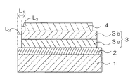
- FIG. 1 Another embodiment of the above embodiment is shown in FIG. This is shown in FIG. 1 in that the side surface of the power generation layer 3 (light absorption layer 3a, buffer layer 3b) is formed so as to be located inside the side surface position of the first electrode layer 2 below the entire circumference. It differs from the CIGS solar cell shown. Since the other structure is the same as that of the CIGS solar battery cell shown in FIG. 1, the description is abbreviate
- This CIGS solar cell can be manufactured as follows, for example. That is, after forming up to the second electrode layer 4, a region from the side surface (end surface) of the second electrode layer 4 to the inner side of 100 ⁇ m is cut by a mechanical scriber, and the second electrode layer 4 in the region is removed (L 1 ).
- the shortest distance from the side surface of the second electrode layer 4 to the side surface of the first electrode layer 2 is obtained. Since the distance is long, the occurrence of a short circuit can be suppressed more effectively.
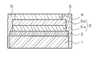
- FIG. 3 Still another embodiment is shown in FIG. This is formed so that the side surfaces of the power generation layer 3 (light absorption layer 3a and buffer layer 3b) are located on the inner side of the side surface of the first electrode layer 2 below the entire circumference. All side surfaces of the electrode layer 2, the power generation layer 3 and the second electrode layer 4 are covered with an insulating coating material 5 over the entire circumference. Since the other structure is the same as that of the CIGS solar cell shown in FIG. 1 or FIG. 3, the description is abbreviate
- This CIGS solar cell can be obtained, for example, by preparing the CIGS solar cell shown in FIG. 3 and coating the side surface with an insulating tape having polyimide.
- the CIGS solar battery cell of the further other embodiment it has the effect of the CIGS solar battery cell shown in FIG. 1 and FIG. 3 and also from the side surface of the second electrode layer 4 to the side surface of the first electrode layer 2. Since the state where the shortest distance is long can be firmly held, the occurrence of a short circuit can be further suppressed.
- the insulating tape having polyimide is preferably used in terms of easy mounting, and examples thereof include a polyimide tape (No. 360UL) manufactured by Nitto Denko Corporation.
- insulation means electrical insulation.
- containing”, “having”, and “including” a certain component are intended to include a case where the component is composed of only that component.
- an insulating tape having polyimide is used as the insulating coating material 5.
- at least the first electrode layer 2 and the second tape are used.
- An insulating material that can cover these side surfaces so that the electrode layer 4 is not in direct contact with the electrode layer 4 can be used.
- the insulating covering material 5 as an insulating covering material capable of covering the side surfaces of the first electrode layer 2 and the second electrode layer 4, at least one of an ethylene vinyl acetate copolymer resin and a urethane resin is used.
- the thermoplastic resin composition to contain is mention
- the adjacent photoelectric conversion elements are maintained in an insulating state only by arranging other photoelectric conversion elements via the adhesive. Since it can fix, it becomes strong with respect to mechanical impacts, such as a bending, and it is preferable at the point which can be set as the photoelectric conversion apparatus excellent in product reliability.
- an insulating coating material 5 formed of a layer made of an inorganic oxide containing at least one selected from the group consisting of SiOx, AlOx, MgOx and ZrOx is used, the external environment changes such as humidity and temperature. It is preferable in that it can improve durability and can be excellent in product reliability.
- ethylene vinyl acetate copolymer resin examples include Ultra Pearl PV (manufactured by Sunvic) and EVASOFT (manufactured by Bridgestone).
- a urethane-silyl adhesive is preferably used from the viewpoint of water resistance, and examples thereof include # 05140 manufactured by Konishi Co., Ltd.
- the layer made of an inorganic oxide containing at least one selected from the group consisting of SiOx, AlOx, MgOx and ZrOx is a vacuum process such as a vapor deposition method, a sputtering method or a plasma CVD method, or a wet process such as a sol-gel method.
- a vacuum process such as a vapor deposition method, a sputtering method or a plasma CVD method, or a wet process such as a sol-gel method.
- These inorganic oxides may be formed of a single material or a plurality of different types. Moreover, it is good also as a layer which combined the some material, and may laminate
- covering material 5 is arrange
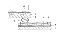
- FIG. 1 An outline of the photoelectric conversion device of the present invention is shown in FIG.
- This is a CIGS solar cell module in which a plurality of CIGS solar cells obtained in the above embodiment are provided and their adjacent edges are overlapped and electrically connected.
- a plurality of CIGS solar cells are electrically connected in series, and a practical voltage can be obtained.
- the electrical connection of the CIGS solar cells is performed between the edge of the first electrode layer 2 in one CIGS solar cell and the second electrode layer 4 in the other CIGS solar cell.
- This can be realized by overlapping the edge portion via the solder 6.
- a conductive film may be interposed between the CIGS solar battery cell and the solder 6.
- the CIGS solar cell module in which CIGS solar cells are electrically connected is usually sealed entirely with a weather-resistant sealing film or the like.
- each CIGS solar cell is not short-circuited, so that no voltage drop occurs and excellent performance can be maintained for a long period of time.
- Example 1 First, a substrate 1 of stainless steel foil SUS430 (size 10 ⁇ 100 mm, thickness 50 ⁇ m) was prepared, and a first electrode layer 2 made of Mo and having a thickness of 500 nm was laminated thereon. Next, the substrate 1 on which the first electrode layer 2 is formed is carried into a vacuum vapor deposition apparatus, and gallium selenide (thickness 400 nm) is formed on the first electrode layer 2 in a state where the substrate temperature is maintained at 420 ° C. ) And indium selenide (thickness 1000 nm) were laminated in this order to form a layer ( ⁇ ) containing selenium, gallium and indium.
- the laminate on which the CIGS layer is formed is cooled, the substrate temperature is maintained at 400 ° C., and NaF is vacuum-deposited on the CIGS layer using a NaF deposition source set at 750 ° C., and then The substrate temperature was heated to 420 ° C., and the substrate temperature was maintained for 10 minutes, whereby Na was diffused into the grain boundaries of the CIGS layer to form the light absorption layer 3a.
- a buffer layer 3b having a CdS layer (thickness 50 nm) and a ZnO layer (thickness 70 nm) and a second electrode layer 4 (thickness 200 nm) made of ITO were laminated in this order on the light absorption layer 3a.
- the second electrode layer 4 in the region from the side surface (end surface) of the second electrode layer 4 to the inner side of 50 ⁇ m is removed by mechanical scribing, and the side surface of the second electrode layer 4 generates power over the entire circumference.
- the CIGS solar cell was manufactured by forming the layer 3 (light absorption layer 3a, buffer layer 3b) so as to be located 50 ⁇ m inside from the side surface position.
- Example 2 Except that the second electrode layer 4 is formed so that the side surface of the second electrode layer 4 is located 500 ⁇ m inward from the side surface position of the power generation layer 3 (light absorption layer 3a, buffer layer 3b) over the entire circumference. CIGS solar cells were manufactured.
- Example 3 Further, an Nd: YAG laser beam is irradiated to a region from the side surface (end surface) of the power generation layer 3 (light absorption layer 3a, buffer layer 3b) to the inner side of 20 ⁇ m, and the power generation layer 3 (light absorption layer 3a, buffer buffer) in the region is irradiated.
- a CIGS solar cell was produced in the same manner as in Example 1 except that the layer 3b) was removed.
- the side surface of the second electrode layer 4 is located 30 ⁇ m inward from the side surface position of the power generation layer 3 (light absorption layer 3a, buffer layer 3b) over the entire circumference, and the power generation layer 3 (light absorption layer) 3a, the side surfaces of the buffer layer 3b) are located 20 ⁇ m inside the side surface position of the first electrode layer 2 over the entire circumference (see FIG. 3).
- Example 4 to 10 Except for covering all sides of the substrate 1, the first electrode layer 2, the power generation layer 3 and the second electrode layer 4 with an insulating coating material shown in Table 1 to be described later, in the same manner as in Example 3, CIGS solar cells were produced.
- Example 1 A CIGS solar cell was manufactured in the same manner as in Example 1 except that the second electrode layer 4 in the region from the side surface (end surface) of the second electrode layer 4 to the inside of 50 ⁇ m was not removed. That is, the CIGS solar battery cell of Comparative Example 1 is formed such that the side surface of the second electrode layer 4 and the side surface of the power generation layer 3 (light absorption layer 3a, buffer layer 3b) are in the same position in plan view. Yes.
- the reverse saturation current in the dark of the CIGS solar cells of Examples 1 to 10 and Comparative Examples 1 and 2 was measured according to the following procedure. Further, the CIGS solar battery cells of Examples 1 to 10 and Comparative Examples 1 and 2 were electrically connected by using three solders, and CIGS solar battery modules corresponding to each of them were manufactured. And the whole surface of these CIGS solar cell modules was coat
- the CIGS solar battery cell has been described as an example of the photoelectric conversion element, but the same effect can be obtained even when other types of solar battery cells are used.
- the photoelectric conversion element of the present invention is effectively prevented from being short-circuited, high conversion efficiency can be achieved at low cost.
- the photoelectric conversion device provided with this photoelectric conversion element is suitably used for a photoelectric conversion device that is required to exhibit high specifications over a long period of time.
Landscapes
- Photovoltaic Devices (AREA)
Abstract
良好な特性を有する光電変換素子およびそれを用いた光電変換装置を提供するため、基板1と、第1電極層2と、発電層3と、第2電極層4とをこの順に有する略板状の光電変換素子において、上記第2電極層4の側面を、全周にわたって上記発電層3の側面位置より内側に位置するよう形成した。
Description
本発明は、良好な特性を有する光電変換素子およびそれらを電気的に接続して用いる光電変換装置に関するものである。
従来、光電変換装置として、基板、第1電極層、発電層、第2電極層を備えた光電変換素子を複数備え、隣り合う光電変換素子の縁部同士を重ね合せた状態で半田等により電気的に接続させたものが知られている(例えば、特許文献1参照)。このものは、複数の光電変換素子を電気的に接続させることにより、実用的な電圧を得ることができるようになっている。
ところで、このような光電変換装置に用いられる光電変換素子は、通常、図7(a)に示す構造を有しており、発電層3を含む各層は極めて薄く形成されている。したがって、図7(b)に示すように、発電層3の端部が欠けると、第2電極層4が白抜き矢印の方向に撓み易くなり、第2電極層4が第1電極層2に接触し、光電変換素子の短絡を起こすことがある。また、光電変換素子の製造中もしくは製造後に、第1電極層2と第2電極層4とを跨ぐように導電性ダストが付着することによって、光電変換素子が短絡を起こすこともある。短絡を起こした光電変換素子を1つでも備えると光電変換装置は全体として電圧の低下が生じるため、光電変換素子における短絡の発生は、光電変換装置としても大きな問題となっている。
本発明は、このような事情に鑑みなされたもので、発電層端部に生じる欠けや微細な導電性ダストの付着に起因する短絡を効果的に防止できる光電変換素子およびそれを用いた光電変換装置の提供をその目的とする。
上記目的を達成するため、本発明は、少なくとも基板と、第1電極層と、発電層と、第2電極層とをこの順に有する略板状の光電変換素子であって、上記第2電極層の側面が、全周にわたって上記発電層の側面位置より内側に位置するよう形成されている光電変換素子を第1の要旨とする。
そして、本発明は、光電変換素子を複数備え、それらの光電変換素子の隣り合う縁部同士を重ね合せて電気的に接続した光電変換装置であって、上記各光電変換素子が、少なくとも基板と、第1電極層と、発電層と、第2電極層とをこの順に有する略板形状を有し、上記第2電極層の側面が、全周にわたって上記発電層の側面位置より内側に位置するよう形成された第1の要旨の光電変換素子である光電変換装置を第2の要旨とする。
すなわち、本発明者らは、高品質の光電変換装置を得るため、その電圧低下の原因となる光電変換素子の短絡を効果的に防止する方法について、種々の検討を重ねた。その結果、各層が積層された光電変換素子の側面部分を工夫することにより、優れた短絡防止効果が得られることを見い出し、本発明に想到した。
なお、本発明において、略板状とは、目視レベルで全体が板状に見えるものであればよいことを意味する。したがって、全体が均一の厚みを有する必要はなく、全体としてみた場合に板状の概念に入るものであればよい。
すなわち、本発明の光電変換素子は、少なくとも基板と、第1電極層と、発電層と、第2電極層とをこの順に有する略板状の光電変換素子であって、上記第2電極層の側面が、全周にわたって上記発電層の側面位置より内側に位置するような配置で形成されている。このため、発電層の端部に欠けが発生しても、第2電極層の端部が第1電極層側に撓むだけのスペースが生じにくく、第2電極層と第1電極層との接触が効果的に防止されている。よって、本発明の光電変換素子は、短絡が効果的に防止されている。また、本発明の光電変換素子は、第1電極層の側面と、第2電極層の側面との最短距離がより長くなるよう形成されているため、光電変換素子の製造中等に導電性ダストが発生したとしても、導電性ダストが第1電極層と第2電極層とを跨ぐように付着する可能性は低く、簡単に短絡しないようになっている。
なかでも、上記発電層の側面が、全周にわたって上記第1電極層の側面位置より内側に位置するよう形成されていると、第1電極層の側面から第2電極層の側面までの最短距離をさらに長くすることができるため、光電変換素子の短絡がより起こりにくくなる。
さらに、上記第1電極層の側面と発電層の側面と第2電極層の側面とが、全周にわたって絶縁性被覆材で被覆されるようにすると、外部から光電変換素子に衝撃が加えられた際であっても第1電極層と第2電極層とが接触することを確実に防止できるため、光電変換素子の短絡がより一層起こりにくくなる。
そして、上記側面の全周を被覆する絶縁性被覆材として、ポリイミドを含む絶縁性テープを用いると、貼り付けるだけの簡単な作業で側面の全周を被覆することができるため、光電変換素子は、側面全周の被覆に際し余計な工程が増加することによるダメージを受けることがない。また、ポリイミドを含む絶縁性テープは加工性に優れるため、光電変換素子の側面形状が複雑であっても正確に対応させることが可能であり、寸法精度に優れる。さらに、ポリイミドを含む絶縁性テープは充分な耐熱性を有することから、光電変換素子を光電変換装置に組み込む際の熱衝撃にも充分耐性を有し、絶縁性被覆材としての形状を損なうことがない。
また、上記側面の全周を被覆する絶縁性被覆材として、エチレン酢酸ビニル共重合体樹脂およびウレタン樹脂の少なくとも一方を含む熱可塑性樹脂組成物からなるものを用いると、これらは、光電変換装置を封止する封止材として汎用されている組成物であることから、封止材と同種の組成物を絶縁性被覆材として用いることにより、封止材と絶縁性被覆材との親和性を高めることができ、より製品信頼性に優れる光電変換装置を得ることができる。
さらに、上記側面の全周を被覆する絶縁性被覆材として、ポリエチレンを含む接着剤からなるものを用いると、その硬化前に、上記接着剤を介して他の光電変換素子を配置するだけで、絶縁性を維持した状態で、隣り合う光電変換素子を固定することができる。このような光電変換装置は、曲げ等の機械的衝撃に対して強いため、より製品信頼性に優れる。
そして、上記側面の全周を被覆する絶縁性被覆材として、SiOx、AlOx、MgOxおよびZrOxからなる群から選ばれた少なくとも1つを含む無機系酸化物によって形成されたものを用いると、光電変換素子の湿度および温度等の外部環境変化に対する耐久性を高めることができる。このため、このような光電変換素子を用いた光電変換装置は、より製品信頼性に優れる。
さらに、光電変換素子を複数備え、それらの光電変換素子の隣り合う縁部同士を重ね合せて電気的に接続した光電変換装置であって、上記各光電変換素子が、少なくとも基板と、第1電極層と、発電層と、第2電極層とをこの順に有する略板形状を有し、上記第2電極層の側面が、全周にわたって上記発電層の側面位置より内側に位置するよう形成する光電変換装置によると、光電変換素子の短絡に起因する電圧の低下が効果的に防止され、低コストで、優れた性能を有する光電変換装置とすることができる。
つぎに、本発明を実施するための形態について説明する。
<光電変換素子>
図1は、本発明の一実施の形態により得られる光電変換素子を模式的に示す断面図である。この光電変換素子は、基板1、第1電極層2、光吸収層3aとバッファ層3bとからなる発電層3、第2電極層4がこの順で積層されたCIGS太陽電池セルであり、図2に示すように、第2電極層4の側面が、全周にわたって発電層3(光吸収層3aおよびバッファ層3b)の側面の位置より長さL1だけ内側に位置するよう形成されている。そして、このCIGS太陽電池セルに第2電極層4側から光を照射すると、光吸収層3aとバッファ層3bとの界面でpn接合が形成されているので、電流を発生させることができるようになっている。なお、光吸収層3a内でpn接合が形成できる場合は、バッファ層3bは必ずしも必要ではない。以下に、このCIGS太陽電池セルを詳しく説明する。なお、図1において、各部分は模式的に示したものであり、実際の厚み,大きさ等とは異なっている(以下の図においても同じ)。また、ある層の側面が、ある層の側面位置より「内側に位置する」とは、光電変換素子を上から見た場合(平面図において)に、ある層の側面の配置が、その下の層の側面の配置より、光電変換素子の中心側に位置することを意味する。
図1は、本発明の一実施の形態により得られる光電変換素子を模式的に示す断面図である。この光電変換素子は、基板1、第1電極層2、光吸収層3aとバッファ層3bとからなる発電層3、第2電極層4がこの順で積層されたCIGS太陽電池セルであり、図2に示すように、第2電極層4の側面が、全周にわたって発電層3(光吸収層3aおよびバッファ層3b)の側面の位置より長さL1だけ内側に位置するよう形成されている。そして、このCIGS太陽電池セルに第2電極層4側から光を照射すると、光吸収層3aとバッファ層3bとの界面でpn接合が形成されているので、電流を発生させることができるようになっている。なお、光吸収層3a内でpn接合が形成できる場合は、バッファ層3bは必ずしも必要ではない。以下に、このCIGS太陽電池セルを詳しく説明する。なお、図1において、各部分は模式的に示したものであり、実際の厚み,大きさ等とは異なっている(以下の図においても同じ)。また、ある層の側面が、ある層の側面位置より「内側に位置する」とは、光電変換素子を上から見た場合(平面図において)に、ある層の側面の配置が、その下の層の側面の配置より、光電変換素子の中心側に位置することを意味する。
すなわち、このCIGS太陽電池セルは、基板1として、幅W=10mm、長さL=100mm、厚み50μmのステンレス箔(SUS)が用いられ、基板1の上に、モリブデン(Mo)からなる厚み500nmの第1電極層2が形成されている。そして、上記第1電極層2の上に、Cu、In、Ga、Seの4元素を有するカルコパイライト型結晶構造の化合物半導体からなる光吸収層3a(厚み2000nm)と、CdS層(厚み50nm、図示せず)とZnO層(厚み70nm、図示せず)とからなるバッファ層3bとを有する発電層3と、がこの順で形成されている(図1に戻る)。さらに、発電層3(バッファ層3b)の上に、ITOからなる厚み200nmの第2電極層4が、その側面が、全周にわたって発電層3(光吸収層3aおよびバッファ層3b)の側面位置より長さL1(この例ではL1=50μm)だけ内側に位置するよう形成されている。
上記構成のCIGS太陽電池セルによれば、第2電極層4の側面が、発電層3の側面位置より全周にわたって長さL1=50μm内側に位置するため、発電層3の端部に欠けが発生しても、第2電極層4の端部が第1電極層2側に撓むことのできるスペースがほとんどなく、第2電極層4が第1電極層2に接触するおそれが少ない。よって、このCIGS太陽電池セルは、簡単に短絡することがない。また、このCIGS太陽電池セルは、第2電極層4の側面から第1電極層2の側面までの最短距離がより長くなっているため、CIGS太陽電池セルの製造中または製造後に、第1電極層2と第2電極層4とを跨ぐように導電性ダストが付着する可能性が極めて低く、簡単に短絡することがない。このように、上記CIGS太陽電池セルは、長期にわたって優れた性能を発揮することができる。
なお、上記実施の形態では、第2電極層4の側面が、全周にわたって発電層3の側面位置より50μm内側に位置するようにしているが(L1=50μm)、第2電極層4の側面位置はこれに限るものではない。しかし、上記L1は5~1000μmであると好ましい。すなわち、L1が5μm未満になると、典型的なクリーンルーム(ISO14644)中に存在する0.1~5μmのダストが導電性であった場合に、このダストが第1電極層2と第2電極層4とを跨ぐように付着して短絡が発生するおそれがあるためである。また、L1が1000μmを超える場合は、第2電極層4に覆われずに露出している発電層3の部分が広くなりすぎて、水分やその他の不純物によって侵され、光電変換特性を下げる傾向がみられるためである。
そして、上記実施の形態では、基板1としてステンレス箔(SUS)を用いているが、これ以外にも、ガラス基板、金属基板、樹脂基板等のなかから、目的や設計の必要に応じて適宜のものを用いることができる。上記ガラス基板としては青板ガラス、アルカリ金属元素の含有量が極めて低い低アルカリガラス(高歪点ガラス)、アルカリ金属元素を含まない無アルカリガラス等があげられる。
また、上記CIGS太陽電池セルを、ロールトゥロール方式またはステッピングロール方式で製造する場合、上記基板1は、長尺状で可撓性を有することが好適である。なお、上記「長尺状」とは長さ方向の長さが幅方向の長さの10倍以上あるものをいい、30倍以上あるものがより好ましく用いられる。
そして、上記実施の形態では、基板1の厚みを、50μmとしているが、これ以外の厚みの基板を使用しても差し支えない。しかし、基板1の厚みは、30μm以上200μm以下の範囲にあることが好ましく、より好ましくは50μm以上100μm以下の範囲である。すなわち、厚みが厚すぎると、CIGS太陽電池セルの屈曲性が失われ、曲げた際にかかる応力が大きくなってその内部構造にダメージを与えるおそれがあり、逆に薄すぎると、CIGS太陽電池セルを製造する際に、基板1が座屈し、CIGS太陽電池セルの製品不良率が上昇する傾向がみられるためである。
また、上記実施の形態では、第1電極層2の形成材料として、モリブデン(Mo)を用いているが、それ以外にも、W、Cr、Ti等を用いることができる。そして、第1電極層2は、単層でなく、複層であってもよい。また、その厚み(複層の場合は、各層の厚みの合計)は、50nm以上1000nm以下であることが好ましい。
そして、上記実施の形態では、上記第1電極層2の上に形成される光吸収層3aの厚みを2000nmとしているが、これ以外の厚みで形成しても差し支えない。しかし、光吸収層3aの厚みは、1.0μm以上3.0μm以下の範囲にあることが好ましく、1.5μm以上2.5μm以下の範囲にあることがより好ましい。厚みが薄すぎると、光吸収量が少なくなり、CIGS太陽電池セルの性能が低下する傾向がみられ、逆に、厚すぎると、光吸収層3aの形成にかかる時間が増加し、生産性に劣る傾向がみられるためである。
また、上記光吸収層3aにおけるCu、In、Gaの組成比は、0.7<Cu/(Ga+In)<0.95(モル比)の式を満たすことが好ましい。この式を満たすようになっていると、上記光吸収層3a内にCu(2-x) Seが過剰に取り込まれることをより阻止でき、しかも層全体としてわずかにCuが不足した状態にできるためである。また、上記光吸収層3aにおいて、同属元素であるGaとInとの比は、0.10<Ga/(Ga+In)<0.60(モル比)の範囲にあることが好ましい。
そして、上記実施の形態では、上記光吸収層3aの上に形成されるバッファ層3bは、基板1側に形成されるCdS層(厚み50nm、図示せず)とZnO層(厚み70nm、図示せず)とを有するようにしているが、バッファ層3bの形成材料としては、CdS、ZnO以外にも、ZnMgO、Zn(OH)2、In2O3、In2S3、これらの混晶であるZn(O,S,OH)等を用いることができる。また、上記光吸収層3aとpn結合できる高抵抗のn型半導体を用いる等の場合には、バッファ層3bを単層とすることもできる。また、バッファ層3bの厚みは、単層および複層のいずれの場合であっても、30nm以上200nm以下であることが好ましい。
さらに、上記実施の形態では、上記バッファ層3bの上に形成される第2電極層4の形成材料として、ITOを用いているが、その他にも、ZnO、In2O3、SnO2等の透光率の高い材料を用いることができる。また、上記実施の形態では、第2電極層4の厚みを200nmとしているが、これ以外の厚みに形成してもよい。しかし、第2電極層4の厚みは、光透過性および電気伝導性の観点から、100nm以上2000nm以下であることが好ましい。
また、第2電極層4の形成材料としては、電気伝導性を高める目的で、あるいはバンドアライメントを調整する目的で、第2電極層4の材料に少量のドーピング材料を含ませたものも好適に用いられる。このようなドーピング材料としては、例えば、Al:ZnO(AZO)、B:ZnO(BZO)、Ga:ZnO(GZO)、Sn:In2O3(ITO)、F:SnO2(FTO)、Zn:In2O3、Ti:In2Oe、Zr:In2O3、W:In2O3があげられる。
なお、上記の実施の形態では用いていないが、基板1由来の不純物がCIGS太陽電池セルに悪影響を及ぼすおそれがある場合には、基板1の上に、不純物拡散防止層を設けることが好ましい。このような不純物拡散防止層の形成材料としては、Cr、SiO2、Al2O3、TiN、TiO2、Ni、NiCr、Co等を用いることができる。その厚みは、効果とコストとのバランスの観点から、50nm以上1000nm以下であることが好ましい。そして、不純物拡散防止層は、基板1の上ではなく、第1電極層2の上に形成することもできる。
このようなCIGS太陽電池セルは、例えば、つぎのような方法で製造することができる。すなわち、まず、長尺状の基板1を準備し、その表面に第1電極層2を形成し、その上に光吸収層3aを形成し、これを所定のサイズとなるよう切断した後、上記光吸収層3aの上に、バッファ層3b、第2電極層4をこの順で積層する。ついで、上記第2電極層4について、第2電極層4の側面(端面)から所定位置までの内側の領域をメカニカルスクライブにて除去する。これにより、第2電極層4の側面が全周にわたって発電層3(光吸収層3a,バッファ層3b)の側面位置より、内側に位置するCIGS太陽電池セルを得ることができる。以下、この製法を、各層の形成工程ごとに詳細に説明する。
〔第1電極層2の形成まで〕
長尺状のSUSからなる基板1を準備し、ロールトゥロール方式により、基板1を走行させながら、その表面に、スパッタリング法により厚み500nmのMoからなる第1電極層2を形成する。
長尺状のSUSからなる基板1を準備し、ロールトゥロール方式により、基板1を走行させながら、その表面に、スパッタリング法により厚み500nmのMoからなる第1電極層2を形成する。
〔光吸収層3aの形成〕
上記第1電極層2上に、基板1を420℃に保持した状態で、セレン化ガリウムとセレン化インジウムとを固相状態でこの順で積層し、インジウムとガリウムとセレンとを有する層(α)を形成する。そして、基板1の温度を420℃に保ったままの状態で、上記層(α)上にセレン化銅を積層し、銅とセレンとを有する層(β)を形成する。基板1上に、第1電極層2、層(α)および層(β)が積層された積層体に対し、微量のSe蒸気を供給しつつ、基板1の温度を650℃とし、その状態を15分間保持する。これにより、上記層(β)が液相状態となり、この層(β)中の銅が層(α)中に拡散し、結晶が成長する。ついで、基板1の温度を650℃に保った状態で、微量のSe蒸気を供給しつつ、Gaの蒸着量を徐々に増加させながら、In、Ga、Seを蒸着し、厚み2000nmのCIGS層を形成する。そして、このCIGS層の上にNaFを蒸着し、その後、基板1の温度を420℃とし、その状態を10分間保持することにより、CIGS層の粒界へNaを拡散させて、光吸収層3aを形成する。
上記第1電極層2上に、基板1を420℃に保持した状態で、セレン化ガリウムとセレン化インジウムとを固相状態でこの順で積層し、インジウムとガリウムとセレンとを有する層(α)を形成する。そして、基板1の温度を420℃に保ったままの状態で、上記層(α)上にセレン化銅を積層し、銅とセレンとを有する層(β)を形成する。基板1上に、第1電極層2、層(α)および層(β)が積層された積層体に対し、微量のSe蒸気を供給しつつ、基板1の温度を650℃とし、その状態を15分間保持する。これにより、上記層(β)が液相状態となり、この層(β)中の銅が層(α)中に拡散し、結晶が成長する。ついで、基板1の温度を650℃に保った状態で、微量のSe蒸気を供給しつつ、Gaの蒸着量を徐々に増加させながら、In、Ga、Seを蒸着し、厚み2000nmのCIGS層を形成する。そして、このCIGS層の上にNaFを蒸着し、その後、基板1の温度を420℃とし、その状態を10分間保持することにより、CIGS層の粒界へNaを拡散させて、光吸収層3aを形成する。
なお、本発明において、固相とは、その温度において固体状態にある相のことをいい、液相とは、その温度において液体状態にある相のことをいう。また、気相とは、その温度において気体状態にある相のことを意味する。
〔バッファ層3bの形成〕
上記ロールトゥロール方式によって第1電極層2および光吸収層3aが形成され、ロール状に巻き取られた基板1を、再度巻き出しながら、切断装置を用いて、これを所定の長さごとに切断して、所定サイズの積層体(基板1+第1電極層2+光吸収層3a)を得る。そして、この積層体の光吸収層3aの上に、溶液成長法(CBD法)によりCdS層(厚み50nm)を形成し、さらにこのCdS層の上に、スパッタリング法によりZnO層(厚み70nm)を形成することにより、CdS層とZnO層とからなるバッファ層3bを形成する。
上記ロールトゥロール方式によって第1電極層2および光吸収層3aが形成され、ロール状に巻き取られた基板1を、再度巻き出しながら、切断装置を用いて、これを所定の長さごとに切断して、所定サイズの積層体(基板1+第1電極層2+光吸収層3a)を得る。そして、この積層体の光吸収層3aの上に、溶液成長法(CBD法)によりCdS層(厚み50nm)を形成し、さらにこのCdS層の上に、スパッタリング法によりZnO層(厚み70nm)を形成することにより、CdS層とZnO層とからなるバッファ層3bを形成する。
〔第2電極層4の形成工程〕
上記バッファ層3bの上に、スパッタリング法によりITOからなる第2電極層4(厚み200nm)を形成する。ついで、その側面(端部)から50μm内側までの領域にメカニカルスクライバを用いて、その領域内の第2電極層4を除去することにより、第2電極層4の側面が全周にわたって発電層3(光吸収層3a,バッファ層3b)の側面から、長さL1=50μmだけ内側に位置するように形成する。なお、この第2電極層4の上に、グリッド形状等の取り出し電極(図示せず)を、第1電極層2と同様の手法を用いて形成するようにしてもよい。このようにして、CIGS太陽電池セルを得ることができる。
上記バッファ層3bの上に、スパッタリング法によりITOからなる第2電極層4(厚み200nm)を形成する。ついで、その側面(端部)から50μm内側までの領域にメカニカルスクライバを用いて、その領域内の第2電極層4を除去することにより、第2電極層4の側面が全周にわたって発電層3(光吸収層3a,バッファ層3b)の側面から、長さL1=50μmだけ内側に位置するように形成する。なお、この第2電極層4の上に、グリッド形状等の取り出し電極(図示せず)を、第1電極層2と同様の手法を用いて形成するようにしてもよい。このようにして、CIGS太陽電池セルを得ることができる。
この方法によれば、短絡の発生を効果的に防止できる優れたCIGS太陽電池セルを、汎用の蒸着装置(ロールトゥロール方式)で連続的に形成することができるため、製造の効率化と低コスト化を図ることができる。
なお、上記実施の形態では、光吸収層3aまでをロールトゥロールにより形成するようにしているが、基板1サイズを調整する等して、枚葉ごとに形成するようにしてもよい。また、第1電極層2をいずれもスパッタリング法により形成しているが、蒸着法、インクジェット法、電解めっき法等を用いて形成するようにしてもよい。
さらに、上記の実施の形態では、光吸収層3aに対するNaの添加を、NaFを用いて行うようにしているが、Na2Se、Na2S等の他のNa化合物を用いて行うようにしてもよい。また、上記の実施の形態では、光吸収層3aに対するNaの添加を、NaFを蒸着しポストアニールする方法により行うようにしているが、光吸収層3aの形成前に、NaFを第1電極層2上に蒸着させる等の方法により行うようにしてもよい。
そして、上記の実施の形態では、CdS層を溶液成長法(CBD法)により形成し、ZnO層をスパッタリング法により形成しているが、これらの層は、それ以外の方法によっても形成することができ、また、真空中、大気中および水溶液中のいずれにおいても形成することができる。例えば、真空中で行う方法としては、スパッタリング法の他、分子線エピタキシー法、電子線蒸着法、抵抗加熱蒸着法、プラズマCVD法、有機金属蒸着法等があげられる。また、水溶液中で行う方法としては、CBD法、電解めっき法等があげられる。
さらに、上記の実施の形態では、第2電極層4の側面(端部)から50μm内側までの領域を、メカニカルスクライバを用いて除去することにより、第2電極層4の側面が全周にわたって発電層3(光吸収層3a,バッファ層3b)の側面から、長さL1=50μmだけ内側に位置するように形成しているが、それ以外の方法によって形成してもよい。そのような方法としては、例えば、メタルマスクや、フォトレジストなどを用いて、あらかじめ発電層3の端部から50μm内側に第2電極層4が形成されないようにすることがあげられる。
また、上記の実施の形態では、第2電極層4をスパッタリング法により形成しているが、それ以外にも、真空蒸着法、有機金属気相成長法等によって形成することができる。
上記実施の形態の他の形態を、図3に示す。このものは、発電層3(光吸収層3a,バッファ層3b)の側面が、全周にわたってその下の第1電極層2側面位置より内側に位置するよう形成されている点において、図1に示すCIGS太陽電池セルと異なっている。その他の構成は図1に示すCIGS太陽電池セルと同様であるため、その説明を省略する。このCIGS太陽電池セルは、例えばつぎのようにして製造することができる。すなわち、第2電極層4までを形成した後、第2電極層4の側面(端面)から100μm内側までの領域をメカニカルスクライバによって切削し、その領域内の第2電極層4を除去する(L1)。ついで、除去跡から現れた発電層3(光吸収層3a,バッファ層3b)の側面(端面)から50μm内側までの領域をあらためてメカニカルスクライバによって切削し、その領域内の発電層3(光吸収層3a,バッファ層3b)を除去する(L2)。これにより、第2電極層4の側面が、全周にわたって発電層3(光吸収層3a,バッファ層3b)の側面位置より、長さL3=50μmだけ内側に位置するとともに、発電層3(光吸収層3a,バッファ層3b)の側面が、全周にわたって第1電極層2の側面位置より、長さL2=50μmだけ内側に位置するようになる。
上記他の実施の形態のCIGS太陽電池セルによれば、図1のCIGS太陽電池セルの奏する効果を有するほか、より一層、第2電極層4の側面から第1電極層2の側面までの最短距離が長くなっているため、より効果的に短絡の発生を抑制することができる。
なお、上記他の実施の形態では、第2電極層4の側面が、全周にわたって発電層3(光吸収層3a,バッファ層3b)の側面位置より50μmだけ内側に位置する(L3=50μm)とともに、発電層3(光吸収層3a,バッファ層3b)の側面が、全周にわたって第1電極層2の側面位置より50μmだけ内側に位置する(L2=50μm)ようにしているが、これに限るものではない。
さらに他の実施の形態を図4に示す。このものは、発電層3(光吸収層3a,バッファ層3b)の側面が、全周にわたってその下の第1電極層2側面位置より内側に位置するよう形成されており、基板1,第1電極層2,発電層3および第2電極層4の全ての側面が、全周にわたって絶縁性被覆材5で被覆されている。その他の構成は、図1または図3に示すCIGS太陽電池セルと同様であるため、その説明を省略する。このCIGS太陽電池セルは、例えば、図3に示すCIGS太陽電池セルを作製し、その側面を、ポリイミドを有する絶縁性テープで被覆することによって得ることができる。
上記さらに他の実施の形態のCIGS太陽電池セルによれば、図1および図3に示すCIGS太陽電池セルの奏する効果を有するほか、第2電極層4の側面から第1電極層2の側面までの最短距離が長い状態を強固に保持することができるため、より一層、短絡の発生を抑制することができる。
上記ポリイミドを有する絶縁性テープは、装着が容易な点で好適に用いられ、そのようなものとしては、例えば、日東電工社製のポリイミドテープ(No.360UL)があげられる。
なお、本発明において、「絶縁性」とは、電気的な絶縁性を意味するものである。また、ある成分を「含有する」,「有する」,「含む」とは、その成分のみからなる場合も含める趣旨である。
そして、上記さらに他の実施の形態では、絶縁性被覆材5として、ポリイミドを有する絶縁性テープを用いているが、ポリイミドを有する絶縁性テープの他にも、少なくとも第1電極層2と第2電極層4とが、直接、接することがないようこれらの側面を被覆することのできる絶縁性を有するものを用いることができる。
絶縁性被覆材5として、上記第1電極層2と第2電極層4との側面を被覆することのできる絶縁性を有するものとしては、エチレン酢酸ビニル共重合体樹脂およびウレタン樹脂の少なくとも一方を含有する熱可塑性樹脂組成物があげられる。すなわち、エチレン酢酸ビニル共重合樹脂は、光電変換装置を封止する封止材として汎用されている組成物であるため、被覆材と封止材とを同種の組成物を用いることで、光電変換装置の封止材との親和性を高めることができ、製品信頼性に優れる光電変換装置を得ることができる。また、絶縁性被覆材5として、ウレタン樹脂を含有する接着剤を用いると、接着剤を介して他の光電変換素子を配置するだけで、絶縁性を維持した状態で、隣り合う光電変換素子を固定することができるため、曲げ等の機械的衝撃に対して強くなり、製品信頼性に優れる光電変換装置とすることができる点で好ましい。また、SiOx、AlOx、MgOxおよびZrOxからなる群から選ばれる少なくとも1つを含む無機系酸化物からなる層によって形成されたものを絶縁性被覆材5として用いると、湿度および温度等の外部環境変化に対する耐久性を高め、製品信頼性に優れるものとできる点で好ましい。
上記エチレン酢酸ビニル共重合体樹脂としては、例えば、ウルトラパールPV(サンビック社製)、EVASOFT(ブリヂストン社製)があげられる。
上記ウレタン樹脂を含有する接着剤としては、ウレタン-シリル系接着剤が耐水性の点で好適に用いられ、そのようなものとしては、例えば、コニシ社製の#05140があげられる。
さらに、SiOx、AlOx、MgOxおよびZrOxからなる群から選ばれた少なくとも1つ含む無機系酸化物からなる層は、蒸着法、スパッタリング法、プラズマCVD法等の真空プロセスや、ゾルゲル法等のウェットプロセスにて形成することができる。そして、これらの無機系酸化物は、単一材料を単層にしてもよいし、種類の異なるものを複数積層してもよい。また、複数の材料を組み合わせた層としてもよいし、その層を複数積層してもよい。
また、上記さらに他の実施の形態では、絶縁性被覆材5は、基板1から第2電極層4までのすべての層の側面を被覆するように配置されているが、これに限るものではない。しかし、このようにすべての層の側面を被覆すると、基板1から第2電極層4までのすべての層の端面への水分等の侵入を防止でき、より絶縁性が高まる点で好ましい。
<光電変換装置>
つぎに、本発明の光電変換装置の概要を図5に示す。このものは、上記実施の形態で得られたCIGS太陽電池セルを複数備え、その隣り合う縁部同士を重ね合せて電気的に接続したCIGS太陽電池モジュールである。このCIGS太陽電池モジュールは、複数のCIGS太陽電池セルが電気的に直列接続された状態となり、実用的な電圧を得ることができる。
つぎに、本発明の光電変換装置の概要を図5に示す。このものは、上記実施の形態で得られたCIGS太陽電池セルを複数備え、その隣り合う縁部同士を重ね合せて電気的に接続したCIGS太陽電池モジュールである。このCIGS太陽電池モジュールは、複数のCIGS太陽電池セルが電気的に直列接続された状態となり、実用的な電圧を得ることができる。
上記CIGS太陽電池セルの電気的接続は、例えば、図6に示すように、一方のCIGS太陽電池セルにおける第1電極層2の縁部と、他方のCIGS太陽電池セルにおける第2電極層4の縁部とを、半田6を介して重ねることで実現することができる。なお、CIGS太陽電池セルと半田6との間に、導電膜を介在させてもよい。CIGS太陽電池セル同士が電気的に接続されたCIGS太陽電池モジュールは、通常、耐候性を有する封止フィルム等でその全面が封止されている。
このようにして得られたCIGS太陽電池モジュールは、各CIGS太陽電池セルが短絡しないため、電圧の低下が生じず、優れた性能を長期間保つことができる。
つぎに、実施例について、比較例と併せて説明する。ただし、本発明はこれに限定されるものではない。
〔実施例1〕
まず、ステンレス箔SUS430(大きさ10×100mm、厚み50μm)の基板1を用意し、この上に、Moからなる厚み500nmの第1電極層2を積層した。つぎに、第1電極層2が形成された基板1を、真空蒸着装置内に搬入し、基板温度を420℃に保持した状態で、第1電極層2の上に、セレン化ガリウム(厚み400nm)、セレン化インジウム(厚み1000nm)をこの順で積層し、セレンとガリウムとインジウムとを有する層(α)を形成した。つづいて、基板温度を420℃に保ったままの状態で、上記層(α)上にセレン化銅(厚み600nm)を積層し、銅とセレンとを有する層(β)を形成した。これらの層(α)と層(β)とが積層された積層体を、微量のSe蒸気を供給しつつ加熱し、基板温度が650℃の状態を15分間保持し、結晶を成長させ、ついで、微量のSe蒸気を供給しつつ、基板温度を650℃に保った状態で、Gaの蒸着量を徐々に増加させながら、In、Ga、Seを蒸着し、CIGS層(厚み2000nm)を形成した。
まず、ステンレス箔SUS430(大きさ10×100mm、厚み50μm)の基板1を用意し、この上に、Moからなる厚み500nmの第1電極層2を積層した。つぎに、第1電極層2が形成された基板1を、真空蒸着装置内に搬入し、基板温度を420℃に保持した状態で、第1電極層2の上に、セレン化ガリウム(厚み400nm)、セレン化インジウム(厚み1000nm)をこの順で積層し、セレンとガリウムとインジウムとを有する層(α)を形成した。つづいて、基板温度を420℃に保ったままの状態で、上記層(α)上にセレン化銅(厚み600nm)を積層し、銅とセレンとを有する層(β)を形成した。これらの層(α)と層(β)とが積層された積層体を、微量のSe蒸気を供給しつつ加熱し、基板温度が650℃の状態を15分間保持し、結晶を成長させ、ついで、微量のSe蒸気を供給しつつ、基板温度を650℃に保った状態で、Gaの蒸着量を徐々に増加させながら、In、Ga、Seを蒸着し、CIGS層(厚み2000nm)を形成した。
つぎに、上記CIGS層が形成された積層体を冷却し、基板温度を400℃に保持し、750℃に設定されたNaF蒸着源を用いて、CIGS層上にNaFを真空蒸着し、その後、基板温度が420℃になるよう加熱し、その基板温度を10分間保持することにより、CIGS層の粒界にNaを拡散させて、光吸収層3aを形成した。
そして、上記光吸収層3aの上に、CdS層(厚み50nm)とZnO層(厚み70nm)を有するバッファ層3b、ITOからなる第2電極層4(厚み200nm)をこの順に積層した。その後、上記第2電極層4の側面(端面)から50μm内側までの領域をメカニカルスクライブにて、その領域内の第2電極層4を除去し、第2電極層4の側面が全周にわたって発電層3(光吸収層3a,バッファ層3b)の側面位置より、50μmだけ内側に位置するように形成して、CIGS太陽電池セルを製造した。
〔実施例2〕
第2電極層4の側面が、全周にわたって発電層3(光吸収層3a,バッファ層3b)の側面位置より、500μmだけ内側に位置するように形成した以外は、実施例1と同様にして、CIGS太陽電池セルを製造した。
第2電極層4の側面が、全周にわたって発電層3(光吸収層3a,バッファ層3b)の側面位置より、500μmだけ内側に位置するように形成した以外は、実施例1と同様にして、CIGS太陽電池セルを製造した。
〔実施例3〕
さらに、発電層3(光吸収層3a,バッファ層3b)の側面(端面)から20μm内側までの領域にNd:YAGレーザ光を照射し、その領域内の発電層3(光吸収層3a,バッファ層3b)を除去した以外は、実施例1と同様にして、CIGS太陽電池セルを製造した。すなわち、このものは、第2電極層4の側面が、全周にわたって発電層3(光吸収層3a,バッファ層3b)の側面位置より30μmだけ内側に位置するとともに、発電層3(光吸収層3a,バッファ層3b)の側面が、全周にわたって第1電極層2の側面位置より20μmだけ内側に位置している(図3参照)。
さらに、発電層3(光吸収層3a,バッファ層3b)の側面(端面)から20μm内側までの領域にNd:YAGレーザ光を照射し、その領域内の発電層3(光吸収層3a,バッファ層3b)を除去した以外は、実施例1と同様にして、CIGS太陽電池セルを製造した。すなわち、このものは、第2電極層4の側面が、全周にわたって発電層3(光吸収層3a,バッファ層3b)の側面位置より30μmだけ内側に位置するとともに、発電層3(光吸収層3a,バッファ層3b)の側面が、全周にわたって第1電極層2の側面位置より20μmだけ内側に位置している(図3参照)。
〔実施例4~10〕
基板1,第1電極層2,発電層3および第2電極層4の全ての側面を、全周にわたって後記表1に示す絶縁性被覆材で被覆した以外は、実施例3と同様にして、CIGS太陽電池セルを製造した。
基板1,第1電極層2,発電層3および第2電極層4の全ての側面を、全周にわたって後記表1に示す絶縁性被覆材で被覆した以外は、実施例3と同様にして、CIGS太陽電池セルを製造した。
〔比較例1〕
第2電極層4の側面(端面)から50μm内側までの領域内の第2電極層4を除去しなかった以外は、実施例1と同様にしてCIGS太陽電池セルを製造した。すなわち、比較例1のCIGS太陽電池セルは、第2電極層4の側面と発電層3(光吸収層3a,バッファ層3b)の側面とが、平面視において同じ位置になるように形成されている。
第2電極層4の側面(端面)から50μm内側までの領域内の第2電極層4を除去しなかった以外は、実施例1と同様にしてCIGS太陽電池セルを製造した。すなわち、比較例1のCIGS太陽電池セルは、第2電極層4の側面と発電層3(光吸収層3a,バッファ層3b)の側面とが、平面視において同じ位置になるように形成されている。
〔比較例2〕
隣り合うCIGS太陽電池セルと重なる2辺のみ、第2電極層4の側面(端面)から50μm内側までの領域内の第2電極層4を除去し、残りの2辺については、第2電極層4の除去を行わないようにした以外は、実施例1と同様にしてCIGS太陽電池セルを製造した。すなわち、このCIGS太陽電池セルは、第2電極層4の側面が、全周にわたって発電層3の側面位置の内側に位置するものではない。
隣り合うCIGS太陽電池セルと重なる2辺のみ、第2電極層4の側面(端面)から50μm内側までの領域内の第2電極層4を除去し、残りの2辺については、第2電極層4の除去を行わないようにした以外は、実施例1と同様にしてCIGS太陽電池セルを製造した。すなわち、このCIGS太陽電池セルは、第2電極層4の側面が、全周にわたって発電層3の側面位置の内側に位置するものではない。
上記実施例1~10および比較例1,2のCIGS太陽電池セルの暗中での逆飽和電流を、下記の手順に従ってそれぞれ測定した。また、上記実施例1~10および比較例1,2のCIGS太陽電池セルを、3個ずつ半田を用いて電気的に接続し、それぞれに対応するCIGS太陽電池モジュールを製造した。そして、これらのCIGS太陽電池モジュールの全面を可撓性および耐候性を有する透光性のカバーフィルム(三菱樹脂化学社製、ビューバリア)で被覆した。このCIGS太陽電池モジュールの信頼性試験(DH)を下記の手順に従ってそれぞれ
行った。これらの結果を後記の表1に併せて示す。
行った。これらの結果を後記の表1に併せて示す。
〔暗中の逆飽和電流〕
暗中の逆飽和電流の測定は、以下のようにして行った。すなわち、暗中雰囲気で、25℃になるように温度調節した測定ステージ上にCIGS太陽電池セルをのせ、電圧をスイープさせながらその電流を測定し、負バイアスとして-5V印可したときの電流値をCIGS太陽電池セルの暗中の逆飽和電流値として記録した。
暗中の逆飽和電流の測定は、以下のようにして行った。すなわち、暗中雰囲気で、25℃になるように温度調節した測定ステージ上にCIGS太陽電池セルをのせ、電圧をスイープさせながらその電流を測定し、負バイアスとして-5V印可したときの電流値をCIGS太陽電池セルの暗中の逆飽和電流値として記録した。
〔信頼性試験(DH)〕
信頼性試験には、エスペック社の高温恒湿試験機(PL-3J)を用い、85℃、湿度85%に保った雰囲気にCIGS太陽電池モジュールを1000時間さらした。そして、1000時間経過後の光電変換効率の、試験開始前の変換効率に対する比が90%以上のものを合格(○印)とし、90%に満たない物を不合格(×印)として評価した。
信頼性試験には、エスペック社の高温恒湿試験機(PL-3J)を用い、85℃、湿度85%に保った雰囲気にCIGS太陽電池モジュールを1000時間さらした。そして、1000時間経過後の光電変換効率の、試験開始前の変換効率に対する比が90%以上のものを合格(○印)とし、90%に満たない物を不合格(×印)として評価した。

なお、表1に示す絶縁性被覆材は、以下のものを使用した。
*1:ポリイミドテープ(日東電工社製、No.360UL)
*2:エチレン酢酸ビニル共重合体樹脂組成物(サンビック社製、ウルトラパールPV)
*3:ウレタン-シリル系接着剤(コニシ社製、#05140)
*1:ポリイミドテープ(日東電工社製、No.360UL)
*2:エチレン酢酸ビニル共重合体樹脂組成物(サンビック社製、ウルトラパールPV)
*3:ウレタン-シリル系接着剤(コニシ社製、#05140)
上記の結果より、実施例1~10の全てにおいて、CIGS太陽電池モジュールの信頼性試験(DH)が合格しているのに対し、比較例1,2は、いずれも不合格であった。また、実施例のなかでも、基板1,第1電極層2,発電層3および第2電極層4の全ての側面を全周にわたって絶縁性被覆材で被覆した、実施例5~10のCIGS太陽電池セルは、とりわけ暗中の逆飽和電流値が低くなり、優れた短絡防止効果が得られることがわかった。
なお、本発明では、光電変換素子として、CIGS太陽電池セルを例にあげて説明したが、他の方式の太陽電池セルを用いても同様の効果を得ることができる。
上記実施例においては、本発明における具体的な形態について示したが、上記実施例は単なる例示にすぎず、限定的に解釈されるものではない。当業者に明らかな様々な変形は、本発明の範囲内であることが企図されている。
本発明の光電変換素子は、短絡が効果的に防止されているため、低コストで高変換効率を達成できる。また、この光電変換素子を備えた光電変換装置は、高スペックを長期間にわたって発揮することが要求される光電変換装置に好適に用いられる。
1 基板
2 第1電極層
3 発電層
4 第2電極層
2 第1電極層
3 発電層
4 第2電極層
Claims (8)
- 少なくとも基板と、第1電極層と、発電層と、第2電極層とをこの順に有する略板状の光電変換素子であって、上記第2電極層の側面が、全周にわたって上記発電層の側面位置より内側に位置するよう形成されていることを特徴とする光電変換素子。
- 少なくとも基板と、第1電極層と、発電層と、第2電極層とをこの順に有する略板状の光電変換素子であって、上記発電層の側面が、全周にわたって上記第1電極層の側面位置より内側に位置するよう形成されている請求項1記載の光電変換素子。
- 少なくとも基板と、第1電極層と、発電層と、第2電極層とをこの順に有する略板状の光電変換素子であって、上記第1電極層の側面と発電層の側面と第2電極層の側面とが、全周にわたって絶縁性被覆材で被覆されている請求項1または2記載の光電変換素子。
- 上記側面の全周を被覆する絶縁性被覆材が、ポリイミドを含む絶縁性テープである請求項3記載の光電変換素子。
- 上記側面の全周を被覆する絶縁性被覆材が、エチレン酢酸ビニル共重合体樹脂およびウレタン樹脂の少なくとも一方を含む熱可塑性樹脂組成物からなる請求項3記載の光電変換素子。
- 上記側面の全周を被覆する絶縁性被覆材が、ポリエチレンを含む接着剤からなる請求項3記載の光電変換素子。
- 上記側面の全周を被覆する絶縁性被覆材が、SiOx、AlOx、MgOxおよびZrOxからなる群から選ばれた少なくとも1つを含む無機系酸化物によって形成されたものである請求項3記載の光電変換素子。
- 光電変換素子を複数備え、それらの光電変換素子の隣り合う縁部同士を重ね合せて電気的に接続した光電変換装置であって、上記各光電変換素子が、少なくとも基板と、第1電極層と、発電層と、第2電極層とをこの順に有する略板形状を有し、上記第2電極層の側面が、全周にわたって上記発電層の側面位置より内側に位置するよう形成された請求項1~7のいずれか一項に記載の光電変換素子であることを特徴とする光電変換装置。
Applications Claiming Priority (2)
| Application Number | Priority Date | Filing Date | Title |
|---|---|---|---|
| JP2014-258553 | 2014-12-22 | ||
| JP2014258553A JP2016119401A (ja) | 2014-12-22 | 2014-12-22 | 光電変換素子およびそれを用いた光電変換装置 |
Publications (1)
| Publication Number | Publication Date |
|---|---|
| WO2016104230A1 true WO2016104230A1 (ja) | 2016-06-30 |
Family
ID=56150255
Family Applications (1)
| Application Number | Title | Priority Date | Filing Date |
|---|---|---|---|
| PCT/JP2015/084987 Ceased WO2016104230A1 (ja) | 2014-12-22 | 2015-12-15 | 光電変換素子およびそれを用いた光電変換装置 |
Country Status (3)
| Country | Link |
|---|---|
| JP (1) | JP2016119401A (ja) |
| TW (1) | TW201635571A (ja) |
| WO (1) | WO2016104230A1 (ja) |
Families Citing this family (5)
| Publication number | Priority date | Publication date | Assignee | Title |
|---|---|---|---|---|
| WO2019180854A1 (ja) | 2018-03-20 | 2019-09-26 | 株式会社 東芝 | 多接合型太陽電池モジュール及び太陽光発電システム |
| KR20220167085A (ko) * | 2021-06-11 | 2022-12-20 | 상라오 징코 솔라 테크놀러지 디벨롭먼트 컴퍼니, 리미티드 | 태양 전지, 그의 제조 방법 및 그를 포함하는 태양 전지 모듈 |
| WO2023054651A1 (ja) | 2021-09-30 | 2023-04-06 | 出光興産株式会社 | 光電変換モジュール、パドル及び光電変換モジュールの製造方法 |
| US12604541B2 (en) | 2021-09-30 | 2026-04-14 | Idemitsu Kosan Co., Ltd. | Photoelectric conversion module, paddle, and method for manufacturing photoelectric conversion module |
| US20250011010A1 (en) | 2021-10-29 | 2025-01-09 | Idemitsu Kosan Co., Ltd. | Photoelectric conversion module, paddle, and method for manufacturing photoelectric conversion module |
Citations (4)
| Publication number | Priority date | Publication date | Assignee | Title |
|---|---|---|---|---|
| JP2002016269A (ja) * | 2000-06-28 | 2002-01-18 | Mitsubishi Heavy Ind Ltd | 薄膜太陽電池パネルの製造方法及び製造装置 |
| WO2013054600A1 (ja) * | 2011-10-14 | 2013-04-18 | 日東電工株式会社 | 太陽電池セルの製造方法、及び太陽電池モジュール |
| WO2013161127A1 (ja) * | 2012-04-25 | 2013-10-31 | 株式会社カネカ | 太陽電池およびその製造方法、ならびに太陽電池モジュール |
| JP2014199875A (ja) * | 2013-03-29 | 2014-10-23 | 株式会社カネカ | 太陽電池、およびその製造方法、ならびに太陽電池モジュール |
-
2014
- 2014-12-22 JP JP2014258553A patent/JP2016119401A/ja active Pending
-
2015
- 2015-12-15 TW TW104142129A patent/TW201635571A/zh unknown
- 2015-12-15 WO PCT/JP2015/084987 patent/WO2016104230A1/ja not_active Ceased
Patent Citations (4)
| Publication number | Priority date | Publication date | Assignee | Title |
|---|---|---|---|---|
| JP2002016269A (ja) * | 2000-06-28 | 2002-01-18 | Mitsubishi Heavy Ind Ltd | 薄膜太陽電池パネルの製造方法及び製造装置 |
| WO2013054600A1 (ja) * | 2011-10-14 | 2013-04-18 | 日東電工株式会社 | 太陽電池セルの製造方法、及び太陽電池モジュール |
| WO2013161127A1 (ja) * | 2012-04-25 | 2013-10-31 | 株式会社カネカ | 太陽電池およびその製造方法、ならびに太陽電池モジュール |
| JP2014199875A (ja) * | 2013-03-29 | 2014-10-23 | 株式会社カネカ | 太陽電池、およびその製造方法、ならびに太陽電池モジュール |
Also Published As
| Publication number | Publication date |
|---|---|
| TW201635571A (zh) | 2016-10-01 |
| JP2016119401A (ja) | 2016-06-30 |
Similar Documents
| Publication | Publication Date | Title |
|---|---|---|
| KR101081294B1 (ko) | 태양전지 및 이의 제조방법 | |
| US20160284882A1 (en) | Solar Cell | |
| KR20110091683A (ko) | 광기전력 소자 및 그 제조 방법 | |
| WO2016104230A1 (ja) | 光電変換素子およびそれを用いた光電変換装置 | |
| KR20110035715A (ko) | 태양전지 및 이의 제조방법 | |
| JP2014033202A (ja) | 薄膜太陽電池モジュール及びその製造方法 | |
| KR20110035736A (ko) | 태양전지 및 이의 제조방법 | |
| KR101201542B1 (ko) | 박막태양전지 및 그 제조방법 | |
| KR101983422B1 (ko) | Cigs계 화합물 태양 전지 | |
| KR101091253B1 (ko) | 태양전지 및 이의 제조방법 | |
| US20210028322A1 (en) | Photoelectric conversion module and method for manufacturing photoelectric conversion module | |
| KR101114169B1 (ko) | 태양광 발전장치 | |
| CN103988315B (zh) | 太阳能电池装置及其制造方法 | |
| KR101218503B1 (ko) | 얇은 알루미늄 박막을 이용한 태양전지 모듈 제조방법 | |
| US20120315721A1 (en) | Methods of manufacturing a solar cell module | |
| KR101091505B1 (ko) | 태양전지 및 이의 제조방법 | |
| US20120073645A1 (en) | Solar Cell Apparatus and Method of Manufacturing the Same | |
| KR101081122B1 (ko) | 태양전지 및 이의 제조방법 | |
| US9373729B2 (en) | Solar cell and method of manufacturing the same | |
| KR20110043358A (ko) | 태양전지 및 이의 제조방법 | |
| KR20150142414A (ko) | 도전성 금속층을 적용한 p2 패터닝부를 포함하는 박막 태양전지 및 이의 제조방법 | |
| US9570636B2 (en) | Solar cell and method of fabricating the same | |
| KR101063721B1 (ko) | 태양전지 및 이의 제조방법 | |
| KR101231284B1 (ko) | 태양전지 및 이의 제조방법 | |
| KR101034146B1 (ko) | 태양전지 및 이의 제조방법 |
Legal Events
| Date | Code | Title | Description |
|---|---|---|---|
| 121 | Ep: the epo has been informed by wipo that ep was designated in this application |
Ref document number: 15872799 Country of ref document: EP Kind code of ref document: A1 |
|
| NENP | Non-entry into the national phase |
Ref country code: DE |
|
| 122 | Ep: pct application non-entry in european phase |
Ref document number: 15872799 Country of ref document: EP Kind code of ref document: A1 |