WO2016104206A1 - ドーピング方法、ドーピング装置および半導体素子の製造方法 - Google Patents
ドーピング方法、ドーピング装置および半導体素子の製造方法 Download PDFInfo
- Publication number
- WO2016104206A1 WO2016104206A1 PCT/JP2015/084883 JP2015084883W WO2016104206A1 WO 2016104206 A1 WO2016104206 A1 WO 2016104206A1 JP 2015084883 W JP2015084883 W JP 2015084883W WO 2016104206 A1 WO2016104206 A1 WO 2016104206A1
- Authority
- WO
- WIPO (PCT)
- Prior art keywords
- doping
- plasma
- substrate
- processed
- plasma doping
- Prior art date
- Legal status (The legal status is an assumption and is not a legal conclusion. Google has not performed a legal analysis and makes no representation as to the accuracy of the status listed.)
- Ceased
Links
Images





Classifications
-
- H—ELECTRICITY
- H10—SEMICONDUCTOR DEVICES; ELECTRIC SOLID-STATE DEVICES NOT OTHERWISE PROVIDED FOR
- H10P—GENERIC PROCESSES OR APPARATUS FOR THE MANUFACTURE OR TREATMENT OF DEVICES COVERED BY CLASS H10
- H10P32/00—Diffusion of dopants within, into or out of wafers, substrates or parts of devices
- H10P32/10—Diffusion of dopants within, into or out of semiconductor bodies or layers
- H10P32/12—Diffusion of dopants within, into or out of semiconductor bodies or layers between a solid phase and a gaseous phase
- H10P32/1204—Diffusion of dopants within, into or out of semiconductor bodies or layers between a solid phase and a gaseous phase from a plasma phase
-
- H—ELECTRICITY
- H10—SEMICONDUCTOR DEVICES; ELECTRIC SOLID-STATE DEVICES NOT OTHERWISE PROVIDED FOR
- H10P—GENERIC PROCESSES OR APPARATUS FOR THE MANUFACTURE OR TREATMENT OF DEVICES COVERED BY CLASS H10
- H10P32/00—Diffusion of dopants within, into or out of wafers, substrates or parts of devices
-
- H—ELECTRICITY
- H01—ELECTRIC ELEMENTS
- H01J—ELECTRIC DISCHARGE TUBES OR DISCHARGE LAMPS
- H01J37/00—Discharge tubes with provision for introducing objects or material to be exposed to the discharge, e.g. for the purpose of examination or processing thereof
- H01J37/32—Gas-filled discharge tubes
- H01J37/32009—Arrangements for generation of plasma specially adapted for examination or treatment of objects, e.g. plasma sources
- H01J37/32192—Microwave generated discharge
-
- H—ELECTRICITY
- H01—ELECTRIC ELEMENTS
- H01J—ELECTRIC DISCHARGE TUBES OR DISCHARGE LAMPS
- H01J37/00—Discharge tubes with provision for introducing objects or material to be exposed to the discharge, e.g. for the purpose of examination or processing thereof
- H01J37/32—Gas-filled discharge tubes
- H01J37/32009—Arrangements for generation of plasma specially adapted for examination or treatment of objects, e.g. plasma sources
- H01J37/32192—Microwave generated discharge
- H01J37/32266—Means for controlling power transmitted to the plasma
-
- H—ELECTRICITY
- H01—ELECTRIC ELEMENTS
- H01J—ELECTRIC DISCHARGE TUBES OR DISCHARGE LAMPS
- H01J37/00—Discharge tubes with provision for introducing objects or material to be exposed to the discharge, e.g. for the purpose of examination or processing thereof
- H01J37/32—Gas-filled discharge tubes
- H01J37/32009—Arrangements for generation of plasma specially adapted for examination or treatment of objects, e.g. plasma sources
- H01J37/32403—Treating multiple sides of workpieces, e.g. 3D workpieces
-
- H—ELECTRICITY
- H01—ELECTRIC ELEMENTS
- H01J—ELECTRIC DISCHARGE TUBES OR DISCHARGE LAMPS
- H01J37/00—Discharge tubes with provision for introducing objects or material to be exposed to the discharge, e.g. for the purpose of examination or processing thereof
- H01J37/32—Gas-filled discharge tubes
- H01J37/32431—Constructional details of the reactor
- H01J37/32715—Workpiece holder
-
- H—ELECTRICITY
- H10—SEMICONDUCTOR DEVICES; ELECTRIC SOLID-STATE DEVICES NOT OTHERWISE PROVIDED FOR
- H10D—INORGANIC ELECTRIC SEMICONDUCTOR DEVICES
- H10D30/00—Field-effect transistors [FET]
- H10D30/01—Manufacture or treatment
- H10D30/021—Manufacture or treatment of FETs having insulated gates [IGFET]
- H10D30/024—Manufacture or treatment of FETs having insulated gates [IGFET] of fin field-effect transistors [FinFET]
- H10D30/0241—Manufacture or treatment of FETs having insulated gates [IGFET] of fin field-effect transistors [FinFET] doping of vertical sidewalls, e.g. using tilted or multi-angled implants
-
- H—ELECTRICITY
- H10—SEMICONDUCTOR DEVICES; ELECTRIC SOLID-STATE DEVICES NOT OTHERWISE PROVIDED FOR
- H10D—INORGANIC ELECTRIC SEMICONDUCTOR DEVICES
- H10D30/00—Field-effect transistors [FET]
- H10D30/60—Insulated-gate field-effect transistors [IGFET]
- H10D30/62—Fin field-effect transistors [FinFET]
-
- H—ELECTRICITY
- H10—SEMICONDUCTOR DEVICES; ELECTRIC SOLID-STATE DEVICES NOT OTHERWISE PROVIDED FOR
- H10P—GENERIC PROCESSES OR APPARATUS FOR THE MANUFACTURE OR TREATMENT OF DEVICES COVERED BY CLASS H10
- H10P14/00—Formation of materials, e.g. in the shape of layers or pillars
- H10P14/60—Formation of materials, e.g. in the shape of layers or pillars of insulating materials
- H10P14/65—Formation of materials, e.g. in the shape of layers or pillars of insulating materials characterised by treatments performed before or after the formation of the materials
- H10P14/6502—Formation of materials, e.g. in the shape of layers or pillars of insulating materials characterised by treatments performed before or after the formation of the materials of treatments performed before formation of the materials
- H10P14/6512—Formation of materials, e.g. in the shape of layers or pillars of insulating materials characterised by treatments performed before or after the formation of the materials of treatments performed before formation of the materials by exposure to a gas or vapour
- H10P14/6514—Formation of materials, e.g. in the shape of layers or pillars of insulating materials characterised by treatments performed before or after the formation of the materials of treatments performed before formation of the materials by exposure to a gas or vapour by exposure to a plasma
-
- H—ELECTRICITY
- H10—SEMICONDUCTOR DEVICES; ELECTRIC SOLID-STATE DEVICES NOT OTHERWISE PROVIDED FOR
- H10P—GENERIC PROCESSES OR APPARATUS FOR THE MANUFACTURE OR TREATMENT OF DEVICES COVERED BY CLASS H10
- H10P30/00—Ion implantation into wafers, substrates or parts of devices
- H10P30/20—Ion implantation into wafers, substrates or parts of devices into semiconductor materials, e.g. for doping
-
- H—ELECTRICITY
- H10—SEMICONDUCTOR DEVICES; ELECTRIC SOLID-STATE DEVICES NOT OTHERWISE PROVIDED FOR
- H10P—GENERIC PROCESSES OR APPARATUS FOR THE MANUFACTURE OR TREATMENT OF DEVICES COVERED BY CLASS H10
- H10P70/00—Cleaning of wafers, substrates or parts of devices
- H10P70/20—Cleaning during device manufacture
-
- H—ELECTRICITY
- H01—ELECTRIC ELEMENTS
- H01J—ELECTRIC DISCHARGE TUBES OR DISCHARGE LAMPS
- H01J2237/00—Discharge tubes exposing object to beam, e.g. for analysis treatment, etching, imaging
- H01J2237/32—Processing objects by plasma generation
- H01J2237/33—Processing objects by plasma generation characterised by the type of processing
- H01J2237/335—Cleaning
-
- H—ELECTRICITY
- H01—ELECTRIC ELEMENTS
- H01J—ELECTRIC DISCHARGE TUBES OR DISCHARGE LAMPS
- H01J2237/00—Discharge tubes exposing object to beam, e.g. for analysis treatment, etching, imaging
- H01J2237/32—Processing objects by plasma generation
- H01J2237/33—Processing objects by plasma generation characterised by the type of processing
- H01J2237/336—Changing physical properties of treated surfaces
- H01J2237/3365—Plasma source implantation
-
- H—ELECTRICITY
- H01—ELECTRIC ELEMENTS
- H01J—ELECTRIC DISCHARGE TUBES OR DISCHARGE LAMPS
- H01J37/00—Discharge tubes with provision for introducing objects or material to be exposed to the discharge, e.g. for the purpose of examination or processing thereof
- H01J37/32—Gas-filled discharge tubes
- H01J37/32431—Constructional details of the reactor
- H01J37/3244—Gas supply means
Definitions
- the disclosed embodiment relates to a doping method, a doping apparatus, and a method for manufacturing a semiconductor element.
- Semiconductor elements such as LSI (Large Scale Integrated Circuit) and MOS (Metal Oxide Semiconductor) transistors are used for doping, etching, CVD (Chemical Vapor Deposition), sputtering, etc. on a semiconductor substrate (wafer) to be processed. It is manufactured by applying.
- ion doping which is doping using an ion implantation apparatus, and plasma in which dopant radicals and ions are directly implanted into the surface of an object to be processed using plasma.
- a doping technique there is a doping technique.
- a dopant impurity is uniformly injected into a doping target object such as a FinFET (Fin Field Effect Transistor) type semiconductor element having a three-dimensional structure, regardless of the uneven portion of the three-dimensional structure ( Since the demand for conformal doping has become very strong, many doping techniques using plasma have been tried and reported.
- FinFET Fin Field Effect Transistor
- a doping technique plasma doping
- a doping processing apparatus there is a technique in which an ionic plasma is mainly generated, and then the generated ionic plasma is confused to dope the entire three-dimensional structure. is there.
- IADD Ion Assisted Deposition and Doping
- the doping depth from the surface of each part or the dopant at each part of the doping object.
- the background is that high coverage with equal concentration, that is, high conformality (uniformity) in doping is required.
- the conventional technology has a problem that it cannot conformally dope a doping object such as a FinFET type semiconductor device having a three-dimensional structure.
- the amount of ion irradiation with respect to the location where the three-dimensional structure of the FinFET type semiconductor element is hidden as a three-dimensional barrier is smaller than the top of the Fin, so Cannot be conformally doped.
- the substrate surface of the FinFET type semiconductor device is used for the purpose of doping all of the top, side, and bottom of the fin of the FinFET type semiconductor device.
- the ion beam is irradiated at an angle of 45 degrees with respect to. Thereafter, the ion beam is irradiated at an angle of 135 degrees, in other words, at an angle of 45 degrees from the opposite side.
- the fin has a certain height, irradiated ions do not reach the region near the bottom in the height direction of the fin in the side and the bottom.
- the dopant (ion) generated by the plasma is randomly extracted into the three-dimensional form by an ion extraction mechanism called Extension Plate.
- a plasma doping technique characterized by irradiating the surface of a structure is shown.
- the experimental data shown by this method suggests that the thickness of the amorphous layer (the disordered layer of Si crystal containing the dopant) formed on the surface of the three-dimensional structure is conformal.
- this does not indicate that the top and side portions of Fin Body can be both conformally doped with a uniform dopant concentration.
- the layer thickness of the pre-amorphous layer generated as a result of doping is only uniform, and the doping process alone is not conformal.
- the dopant concentration and doping depth implanted at the top position and the side position are implanted.
- the concentration of dopant and the depth of doping, the concentration of dopant implanted at the bottom position and the depth of doping are not uniform, and the doping is not conformal.
- conformality can be achieved by performing an annealing process immediately after doping.
- no method has been established so far for achieving conformality when annealing cannot be performed immediately after doping.
- a mask such as a resist that does not have heat resistance on the element after doping, or if a heat treatment is performed immediately after doping, there is a possibility that a contaminating element may diffuse from the residual film generated by doping. Conformality cannot be achieved by the annealing process.
- the present invention has been made in view of the above, and a doping method, a doping apparatus, and a semiconductor element that can realize conformal doping even when the substrate to be processed cannot be heat-treated immediately after doping. It aims to provide a method.
- the substrate to be processed is cleaned under a predetermined condition after the plasma doping process using the bias power value supplied during the plasma doping process. Is set to a value in which the dopant concentration at the top of the substrate to be processed is substantially equal to the dopant concentration at the side, and the plasma is generated in the processing container using microwaves, and is held on the holding table in the processing container. A plasma doping process is performed on the processed substrate.
- conformal doping can be realized even when the substrate to be processed cannot be heat-treated immediately after doping.
- FIG. 1 is a schematic perspective view showing a part of a FinFET type semiconductor device which is a semiconductor device manufactured by a doping method and a doping apparatus according to the first embodiment.
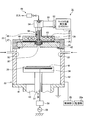
- FIG. 2 is a schematic cross-sectional view showing a main part of the doping apparatus according to the first embodiment.
- FIG. 3 is a flowchart showing a schematic process of the doping method according to the first embodiment.
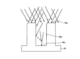
- FIG. 4 is a diagram showing a doping amount with respect to a FinFET type semiconductor device when doping is performed using a plasma doping process.
- FIG. 5 is a diagram showing a relative ratio between the aspect ratio of the FinFET and the concentration of the implanted dopant in the FinFET type semiconductor device.
- FIG. 1 is a schematic perspective view showing a part of a FinFET type semiconductor device which is a semiconductor device manufactured by a doping method and a doping apparatus according to the first embodiment.
- FIG. 2 is a schematic cross-sectional view showing a main part
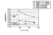
- FIG. 6A shows the value of the bias power supplied in the plasma doping process, the dopant concentration of the substrate to be processed after the plasma doping process, and the SPM (Sulfuric-Acid and Hydroxide Mixture) cleaning after the plasma doping process. It is a graph which shows the relationship with the dopant concentration of a process board
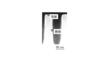
- FIG. 6B is a diagram illustrating a schematic position of a top portion and a side portion of the FinFET type semiconductor device illustrated in FIG. 6A.
- FIG. 7 is an enlarged graph showing a portion showing the dopant concentration after SPM cleaning in the graph shown in FIG. 6A.
- FIG. 8 is a diagram for explaining the relationship between the temperature applied to the holding table and the dopant concentration after SPM cleaning.
- FIG. 9 is a flowchart showing the flow of the method for manufacturing the semiconductor device according to the first embodiment.
- the doping method according to the embodiment is a doping method in which a dopant is implanted into a substrate to be processed, and a bias power value supplied at the time of plasma doping processing is determined based on a cleaning processing performed after plasma doping.
- the bias power value is determined by the dopant concentration at the top of the substrate to be processed and the dopant concentration at the side when the cleaning process is performed after the plasma doping process. You may set to the value which becomes substantially equal.
- the doping apparatus includes a processing container, a gas supply unit that supplies a doping gas and an inert gas for plasma excitation into the processing container, and an object to be processed that has a three-dimensional structure.
- the doping apparatus uses the value of the bias power at which the top dopant concentration and the side dopant concentration of the substrate to be processed are substantially equal when the cleaning process is performed after the plasma doping.
- the control unit further includes a storage unit that stores the conditions, and the control unit controls the plasma generation mechanism to generate plasma in the processing container based on the conditions stored in the storage unit. A plasma doping process may be performed on the processing substrate.
- the semiconductor device manufacturing method includes an acquisition step of acquiring a predetermined value of the bias power as a condition of the plasma doping process on the premise of a cleaning process performed after the plasma doping process, and a predetermined value acquired in the acquisition process.
- the obtaining step sets the bias power value at which the top dopant concentration and the side dopant concentration of the substrate to be processed are substantially equal to each other when the cleaning process is performed. You may get as
- the acquisition step acquires a predetermined value of bias power determined in correlation with a predetermined condition of the cleaning process, and the plasma doping processing step has a predetermined value of 100 W to 400 W. It may be executed while supplying a bias power within the range.
- the dopant concentrations on the top and side portions of the substrate to be processed after the cleaning process are The doping conditions are adjusted to be equal.
- the value of the bias power supplied to the holding table for holding the substrate to be processed during the plasma doping process conformal doping taking into account the influence of the cleaning process is realized.
- conformal doping can be realized by adjusting the conditions of the plasma doping process in consideration of the influence of the cleaning process on the dopant concentration.
- the fin side portion can be realized. Due to high chemical resistance.
- FIG. 1 is a schematic perspective view showing a part of a FinFET type semiconductor device which is a semiconductor device manufactured by a doping method and a doping apparatus according to the first embodiment.
- fins 14 that protrude long upward from a main surface 13 of a silicon substrate 12 are formed in a FinFET type semiconductor device 11 manufactured by a doping method and a doping apparatus according to an embodiment of the present invention.
- the direction in which the fins 14 extend is the direction indicated by the arrow I in FIG.
- the portion of the fin 14 has a substantially rectangular shape when viewed from the direction of the arrow I which is the lateral direction of the FinFET type semiconductor element 11.
- a gate 15 extending in a direction orthogonal to the direction in which the fin 14 extends is formed so as to cover a part of the fin 14.
- the source 16 is formed on the front side of the formed gate 15, and the drain 17 is formed on the back side.
- Doping with plasma generated using microwaves is performed on the shape of the fins 14, that is, the surface of the portion protruding upward from the main surface 13 of the silicon substrate 12.
- a photoresist layer may be formed at a stage before doping is performed.
- the photoresist layer is formed on a side of the fin 14 at a predetermined interval, for example, a portion located in the left-right direction on the paper surface in FIG.
- the photoresist layer is formed so as to extend in the same direction as the fins 14 and to protrude long upward from the main surface 13 of the silicon substrate 12.
- FIG. 2 is a schematic cross-sectional view showing a main part of the doping apparatus according to the first embodiment. In FIG. 2, some of the members are not hatched for easy understanding. In this embodiment, the vertical direction in FIG. 2 is the vertical direction in the doping apparatus.
- a doping apparatus 31 includes a processing container 32 that performs doping on the substrate W to be processed therein, a gas supply unit 33 that supplies a gas for plasma excitation and a doping gas into the processing container 32. Further, a disk-shaped holding table 34 for holding the substrate W to be processed, a plasma generating mechanism 39 for generating plasma in the processing container 32 using microwaves, and a pressure for adjusting the pressure in the processing container 32 An adjustment mechanism, a bias power supply mechanism that supplies AC bias power to the holding table 34, and a control unit 28 that controls the operation of the entire doping apparatus 31 are provided.
- the control unit 28 controls the entire doping apparatus 31 such as the gas flow rate in the gas supply unit 33, the pressure in the processing container 32, and the bias power supplied to the holding table 34.
- the control unit 28 is connected to a storage unit 28a that stores doping process conditions such as bias power.
- the processing container 32 includes a bottom portion 41 located on the lower side of the holding table 34 and a side wall 42 extending upward from the outer periphery of the bottom portion 41.
- the side wall 42 is substantially cylindrical.
- An exhaust hole 43 for exhaust is provided in the bottom 41 of the processing container 32 so as to penetrate a part thereof.
- the upper side of the processing container 32 is open, and a lid 44 disposed on the upper side of the processing container 32, a dielectric window 36 described later, and a seal member interposed between the dielectric window 36 and the lid 44.
- the processing container 32 is configured to be hermetically sealed by an O-ring 45 as a sealing member.
- the gas supply unit 33 includes a first gas supply unit 46 that blows gas toward the center of the substrate to be processed W, and a second gas supply unit 47 that blows gas from the outside of the substrate to be processed W.
- the gas supply hole 30 for supplying a gas in the first gas supply unit 46 is located at the center in the radial direction of the dielectric window 36, and is more dielectric than the lower surface 48 of the dielectric window 36 that is a facing surface facing the holding table 34. It is provided at a position retracted inward of the body window 36.
- the first gas supply unit 46 supplies an inert gas and a doping gas for plasma excitation while adjusting a flow rate and the like by a gas supply system 49 connected to the first gas supply unit 46.
- the second gas supply unit 47 is formed by providing a plurality of gas supply holes 50 for supplying an inert gas and a doping gas for plasma excitation in the processing container 32 in a part on the upper side of the side wall 42. Yes.
- the plurality of gas supply holes 50 are provided at equal intervals in the circumferential direction.
- the first gas supply unit 46 and the second gas supply unit 47 are supplied with the same type of inert gas or doping gas for plasma excitation from the same gas supply source.
- another gas can also be supplied from the 1st gas supply part 46 and the 2nd gas supply part 47, and those flow ratios etc. can also be adjusted.
- a high frequency power source 58 for RF (Radio Frequency) bias is electrically connected to the electrode in the holding table 34 through the matching unit 59.
- the high frequency power supply 58 can output a high frequency of 13.56 MHz, for example, with a predetermined power (bias power).
- the matching unit 59 accommodates a matching unit for matching between the impedance on the high frequency power source 58 side and the impedance on the load side such as an electrode, plasma, and the processing vessel 32, and the matching unit is included in this matching unit.
- a blocking capacitor for self-bias generation is included.
- the supply of the bias voltage to the holding table 34 is appropriately changed as necessary.
- the control unit 28 controls the AC bias power supplied to the holding table 34 as a bias power supply mechanism.
- the holding table 34 can hold the substrate W to be processed thereon by an electrostatic chuck (not shown).
- the holding table 34 is supported by an insulating cylindrical support 51 that extends vertically upward from the lower side of the bottom 41.
- the exhaust hole 43 described above is provided so as to penetrate a part of the bottom 41 of the processing container 32 along the outer periphery of the cylindrical support part 51.
- An exhaust device (not shown) is connected to the lower side of the annular exhaust hole 43 via an exhaust pipe (not shown).
- the exhaust device has a vacuum pump such as a turbo molecular pump.
- the inside of the processing container 32 can be depressurized to a predetermined pressure by the exhaust device.
- the control part 28 adjusts the pressure in the processing container 32 by control of the exhaust_gas
- the plasma generation mechanism 39 is provided outside the processing vessel 32 and includes a microwave generator 35 that generates microwaves for plasma excitation.
- the plasma generation mechanism 39 includes a dielectric window 36 that is disposed at a position facing the holding table 34 and introduces the microwave generated by the microwave generator 35 into the processing container 32.
- the plasma generation mechanism 39 is provided with a plurality of slot holes 40 and is disposed above the dielectric window 36 and includes a slot antenna plate 37 that radiates microwaves to the dielectric window 36.
- the plasma generation mechanism 39 includes a dielectric member 38 that is disposed above the slot antenna plate 37 and that propagates a microwave introduced from a coaxial waveguide 56 described later in the radial direction.
- the microwave generator 35 having the matching 53 is connected to an upper portion of a coaxial waveguide 56 for introducing a microwave through a mode converter 54 and a waveguide 55.
- a TE mode microwave generated by the microwave generator 35 passes through the waveguide 55, is converted to a TEM mode by the mode converter 54, and propagates through the coaxial waveguide 56.
- 2.45 GHz is selected as the frequency of the microwave generated by the microwave generator 35.
- the dielectric window 36 has a substantially disc shape and is made of a dielectric. Specific examples of the material of the dielectric window 36 include quartz and alumina.
- the slot antenna plate 37 has a thin plate shape and a disk shape.
- the slot antenna plate 37 is preferably a radial line slot antenna.
- the microwave generated by the microwave generator 35 is propagated through the coaxial waveguide 56.
- the microwaves radiate radially outward in a region sandwiched between the cooling jacket 52 having a circulation path 60 for circulating the refrigerant therein and adjusting the temperature of the dielectric member 38 and the like and the slot antenna plate 37. And is radiated to the dielectric window 36 from a plurality of slot holes 40 provided in the slot antenna plate 37.
- the microwave transmitted through the dielectric window 36 generates an electric field immediately below the dielectric window 36 and generates plasma in the processing chamber 32.
- the plasma generation mechanism has the dielectric window 36 that is exposed in the processing container 32 and is provided at a position facing the holding table 34.
- the shortest distance between the dielectric window 36 and the substrate W to be processed held by the holding table 34 is 5.5 cm or more and 15 cm or less.
- microwave plasma When microwave plasma is generated in the doping apparatus 31, plasma electrons are generated immediately below the lower surface 48 of the dielectric window 36, specifically, in a region located about several cm below the lower surface 48 of the dielectric window 36. A so-called plasma generation region having a relatively high temperature is formed. A so-called plasma diffusion region in which the plasma generated in the plasma generation region diffuses is formed in the region located on the lower side in the vertical direction. This plasma diffusion region is a region where the electron temperature of plasma is relatively low, and plasma doping processing, that is, doping is performed in this region. Note that when microwave plasma is generated in the doping apparatus 31, the electron density of the plasma becomes relatively high. Then, so-called plasma damage is not given to the substrate W to be processed at the time of doping, and the electron density of plasma is high, so that efficient doping, specifically, for example, doping time can be shortened.
- ICP inductively coupled plasma
- the amount of high-energy ions generated is very large compared to radicals and low-energy ion components in the plasma. Irradiation damage increases at the same time.
- microwave plasma radicals and low-energy ion components can be efficiently generated in a high-pressure zone where the pressure advantageous for forming conformal doping is 100 mTorr or more.
- radicals active species
- it is electrically neutral it is possible to overwhelmingly reduce plasma irradiation damage to the substrate to be processed compared to ions.
- FIG. 3 is a flowchart showing a schematic process of the doping method according to the first embodiment.
- the substrate W to be subjected to the plasma doping process is carried into the doping apparatus 31 and placed on the holding table 34 (step S31). Then, a plasma doping process is performed based on preset doping conditions (step S32). When the plasma doping process is completed, the substrate W to be processed is unloaded from the doping apparatus 31 (step S33). And the to-be-processed substrate W is put in a washing
- the value of the bias power used in the plasma doping process in step S32 is set in consideration of the influence of the SPM cleaning process performed after the plasma doping process on the conformity.
- the dopant concentration in each part of the substrate to be processed is not equally affected by the SPM cleaning process.
- the dopant concentration of each part of the fin of the semiconductor element manufactured by the plasma doping process will be described.
- FIG. 4 is a diagram showing a doping amount with respect to a FinFET type semiconductor device when doping is performed using a plasma doping process.
- the substrate to be processed W is a FinFET type semiconductor element.
- the fins are provided on the substrate W to be processed. As a result, the amount of radicals and low energy ion components reaching each part varies depending on the three-dimensional shape.
- radicals and low-energy ion components generated by a radial slot antenna inject a dopant into the top Wa of the substrate W to be processed and come into contact with the top Wa of the FinFET, and do not contact the top Wa of the FinFET.
- radicals and low energy ion components in contact with the side Wb inject dopants into the side Wb, and radicals and low energy ion components that have not contacted the top or side Wb of the FinFET.
- the radicals and low energy ion components in contact with the bottom Wc will inject the dopant into the bottom Wc.
- the probability of contact with radicals and low-energy ion components in the order of the top portion Wa, the side portion Wb, and the bottom portion Wc of the substrate to be processed W is reduced by the amount of the three-dimensional barrier caused by the FinFET, and the portion is injected accordingly.
- the dopant concentration is also reduced.
- FIG. 5 is a diagram showing a relative ratio between the aspect ratio of the FinFET and the concentration of the implanted dopant in the FinFET type semiconductor device.
- the example shown in FIG. 5 shows a case where reflection and the like are not considered.
- the dopant concentration shown in FIG. 5 shows the case where As (arsenic) is implanted into the silicon substrate.
- As arsenic
- the aspect ratio is “5”, that is, the ratio of the length of the top to the length of the side is “1: 5”
- the dopant is implanted into the bottom when the concentration of the dopant implanted into the top is “1”.
- the concentration of the dopant is about “0.1”.
- FIG. 6A shows the value of bias power (also referred to as RF power or bias power) supplied in the plasma doping process, the dopant concentration of the substrate to be processed after the plasma doping process, and the target after the SPM cleaning after the plasma doping process. It is a graph which shows the relationship with the dopant concentration of the process board
- FIG. 6B is a figure which shows the approximate position of the top part and side part of a FinFET type semiconductor device described in FIG. 6A.
- the plasma doping process used in the example of FIG. 6A is plasma doping using a radial line slot.
- the microwave power was 5 kW
- the pressure in the processing vessel was 230 mTorr.
- the total flow rate of the processing gas was set to 1000 sccm
- the AsH3 (0.7%) / He dilution gas flow rate was set to 440 sccm.
- the remaining gas is He gas.
- the time for performing the plasma doping treatment was 100 seconds.
- the plasma doping process was performed by changing the value of the bias power, that is, the RF power applied to the holding table on which the substrate W to be processed was placed. Then, the dopant concentration (arsenic concentration) at the top and sides of the substrate to be processed immediately after the plasma doping treatment was measured by SEM EDX (Scanning Electron Microscope / Energy Dispersive X-ray Spectroscope).
- an SPM cleaning process was performed on the substrate to be processed after the plasma doping process.
- a 110 ° C. mixed solution with a ratio of H 2 SO 4 (sulfuric acid) and H 2 O 2 (hydrogen peroxide solution) of 4 to 1 was used as the cleaning solution, and the cleaning treatment time was set as follows. 10 minutes.
- concentration) in the top part and side part of the to-be-processed substrate after a SPM cleaning process was measured by SEM EDX.
- the dopant concentration measured under the above conditions is shown in FIG. 6A.
- the dopant concentration at the top of the fin immediately after doping is higher than the dopant concentration at the side of the fin regardless of the value of the RF power.
- the dopant concentration decreases at both the fin top and the fin side.
- the reduction rate is smaller on the fin side than on the fin top.
- the dopant concentration after performing the SPM cleaning treatment for 10 minutes when the RF power is about 400 W or less, the dopant concentration at the fin top is lower than the dopant concentration at the fin side. On the other hand, when the RF power exceeds about 400 W, the dopant concentration at the fin top is higher than the dopant concentration at the fin side. From this, it can be seen that the amount of dopant lost by SPM cleaning is greater at the fin top than at the fin side.
- the reason why the dopant loss due to the SPM cleaning is smaller at the side portion than at the top portion is that the chemical resistance of the side portion is particularly high in the fin subjected to the plasma doping treatment. Therefore, by using the high chemical resistance of the side portion of the FinFET type semiconductor device manufactured by the plasma doping process, the RF power is set so that the dopant concentration of the top portion and the side portion of the semiconductor device after the SPM cleaning becomes equal. For example, conformal doping can be achieved.
- FIG. 7 is an enlarged graph showing a portion showing the dopant concentration after SPM cleaning in the graph shown in FIG. 6A.
- the top dopant concentration and the side dopant concentration after SPM cleaning coincide with each other when the RF power is about 400 W.
- Conformal doping can be realized by performing SPM cleaning after plasma doping if the value of the RF power applied during plasma doping is set so that the dopant concentration is substantially the same between the top and side portions of the semiconductor element after SPM cleaning. .
- step S32 a plasma doping process
- FIG. 8 is a diagram for explaining the relationship between the temperature applied to the holding table 34 (stage) and the dopant concentration after SPM cleaning.
- the data in FIG. 8 was obtained by changing the temperature applied to the holding table 34 and performing the plasma doping process and the SPM cleaning process.
- the left side of FIG. 8 shows dopant profiles after the plasma doping process and after the SPM cleaning process when the temperature of the holding table 34 is adjusted to 300 degrees, 200 degrees, and 60 degrees, respectively.
- the dopant concentration was measured at each position of the top, three sides and the bottom of the fin.
- FIG 8 shows the position of the fin corresponding to each bar graph in the left figure. Note that arsenic was used as the dopant, and SEM EDX was used for the measurement. The SPM cleaning process was performed for about 15 minutes.
- the temperature applied to the holding table 34 may be adjusted using the temperature adjustment mechanism 29 or the like.
- the temperature applied to the holding table 34 is preferably about 150 to 600 degrees.
- FIG. 9 is a flowchart showing a process flow of the semiconductor device manufacturing method according to the first embodiment.
- the semiconductor element manufacturing method shown in FIG. 9 can be realized by using the doping apparatus shown in FIG. 2 and the doping method shown in FIG.
- plasma doping conditions for achieving conformal doping specifically, RF power are specified before performing plasma doping processing.
- plasma doping conditions and cleaning conditions other than the RF power used for manufacturing the semiconductor element are determined (step S81). If the conditions of the doping apparatus and the cleaning apparatus to be used are determined in advance, those conditions may be used.
- step S82 the RF power at which the dopant concentration after the cleaning process substantially matches between the top and the side of the semiconductor element is specified.
- the specified RF power is set as the plasma doping condition, and the other plasma doping conditions determined in step S81 are used to perform the plasma doping process (step S83).
- the semiconductor element subjected to the plasma doping process is cleaned using the cleaning conditions determined in step S81 (step S84). Thereby, a conformal semiconductor device in which the top dopant concentration and the side dopant concentration are substantially equal can be manufactured.
- the value of the bias power supplied during the plasma doping process is set to a predetermined value on the premise of the cleaning process performed after the plasma doping.
- the plasma doping process is performed on the substrate to be processed held on the holding table in the processing container by generating plasma in the processing container using the above.
- the conditions of the plasma doping process are set in consideration of the influence of the cleaning process to be executed thereafter.
- the value of the RF power is set so that conformal doping is achieved after the cleaning process in consideration of the influence of the cleaning process. For this reason, conformal doping can be easily realized by performing a cleaning process after plasma doping.
- the semiconductor device manufacturing method includes an acquisition step of acquiring a predetermined value of a bias power as a condition of the plasma doping process, on the premise of a cleaning process performed after the plasma doping process, and an acquisition process.
- conformal doping can be realized by performing the cleaning process after the plasma doping process. Therefore, conformal doping can be achieved even when it is difficult to perform an annealing process exceeding 500 ° C. immediately after doping. For example, the desired conformality can be achieved even when a mask such as a resist having no heat resistance exists on the doped element. In addition, when heat treatment is performed immediately after doping, conformity can be realized without such a concern even when there is a risk of contamination elements diffusing from the residual film produced by doping.
Landscapes
- Physics & Mathematics (AREA)
- Engineering & Computer Science (AREA)
- Plasma & Fusion (AREA)
- Chemical & Material Sciences (AREA)
- Analytical Chemistry (AREA)
- Insulated Gate Type Field-Effect Transistor (AREA)
Abstract
Description
第1の実施形態では、3次元構造を有する被処理基板に対してドーピング処理を実施した後に洗浄処理を実施することを前提として、洗浄処理後の被処理基板の頂部と側部のドーパント濃度が等しくなるように、ドーピング条件を調整する。特に、プラズマドーピング処理時に被処理基板を保持する保持台に供給するバイアス電力の値を調整することによって、洗浄処理の影響を加味したコンフォーマルドーピングを実現する。
図1は、第1の実施形態に係るドーピング方法及びドーピング装置によって製造される半導体素子であるFinFET型半導体素子の一部を示す概略斜視図である。図1を参照して、この発明の1実施形態に係るドーピング方法及びドーピング装置によって製造されるFinFET型半導体素子11には、シリコン基板12の主表面13から上方向に長く突出したフィン14が形成されている。フィン14の延びる方向は、図1中の矢印Iで示す方向である。フィン14の部分は、FinFET型半導体素子11の横方向である矢印Iの方向から見ると、略矩形状である。フィン14の一部を覆うようにして、フィン14の延びる方向と直交する方向に延びるゲート15が形成されている。フィン14のうち、形成されたゲート15の手前側にソース16が形成されることになり、奥側にドレイン17が形成されることになる。このようなフィン14の形状、すなわち、シリコン基板12の主表面13から上方向に突出した部分の表面に対して、マイクロ波を用いて発生させたプラズマによるドーピングが行われる。
図2は、第1の実施形態に係るドーピング装置の要部を示す概略断面図である。なお、図2において、理解の容易の観点から、部材の一部のハッチングを省略している。また、この実施形態においては、図2における紙面上下方向を、ドーピング装置における上下方向としている。
次に、このようなドーピング装置を用いて、被処理基板Wに対してドーピングを行う方法について説明する。図3は、第1の実施形態に係るドーピング方法の概略的な工程を示すフローチャートである。
一例として、図1に示すようなFinFET型半導体素子をプラズマドーピング処理を用いて製造する場合のフィンの頂部および側部におけるドーパント濃度について説明する。図4は、プラズマドーピング処理を用いてドーピングを行う場合におけるFinFET型半導体素子に対するドーピング量について示す図である。図4に示す例では、被処理基板Wは、FinFET型半導体素子である。ここで、反射などを考慮しない場合、図4に示すように、被処理基板Wにフィンが設けられる結果、立体形状によって、各部に到達するラジカルおよび低エネルギーイオン成分の量が異なる。例えば、ラジアルスロットアンテナによって生成されたラジカルおよび低エネルギーイオン成分は、被処理基板Wのうち、FinFETの頂部Waと接触すると頂部Waにドーパントを注入し、FinFETの頂部Waに接触しなかったラジカルおよび低エネルギーイオン成分のうち側部Wbと接触したラジカルおよび低エネルギーイオン成分が側部Wbにドーパントを注入し、FinFETの頂部Waにも側部Wbにも接触しなかったラジカルおよび低エネルギーイオン成分のうち底部Wcと接触したラジカルおよび低エネルギーイオン成分が底部Wcにドーパントを注入することになる。言い換えると、FinFETによる立体障壁が発生する分、被処理基板Wのうち、頂部Wa、側部Wb、底部Wcの順に、ラジカルおよび低エネルギーイオン成分と接触する確率は低くなり、その分、注入されるドーパントの濃度も低くなる。
図9は、第1の実施形態に係る半導体素子の製造方法の処理の流れを示すフローチャートである。図9に示す半導体素子の製造方法は、図2に示すドーピング装置や図3に示すドーピング方法を用いて実現することができる。
このように、第1の実施形態に係るドーピング方法およびドーピング装置では、プラズマドーピング処理時に供給するバイアス電力の値を、プラズマドーピング後に実施する洗浄処理を前提とした所定値に設定して、マイクロ波を用いて処理容器内にプラズマを発生させることで処理容器内の保持台に保持された被処理基板に対してプラズマドーピング処理を行う。
12 シリコン基板
13 主表面
14 フィン
15 ゲート
16 ソース
17 ドレイン
28 制御部
29 温度調整機構
30 ガス供給孔
31 ドーピング装置
32 処理容器
33 ガス供給部
34 保持台
35 マイクロ波発生器
36 誘電体窓
37 スロットアンテナ板
38 誘電体部材
39 プラズマ発生機構
40 スロット孔
Claims (7)
- 被処理基板にドーパントを注入してドーピングを行うドーピング方法であって、
プラズマドーピング処理時に供給するバイアス電力の値を、プラズマドーピング後に実施する洗浄処理を前提とした所定値に設定して、マイクロ波を用いて処理容器内にプラズマを発生させることで処理容器内の保持台に保持された被処理基板に対してプラズマドーピング処理を行うプラズマドーピング処理工程、
を含むドーピング方法。 - 前記プラズマドーピング処理工程において、前記バイアス電力の値は、前記プラズマドーピング処理後に前記洗浄処理を実施した場合に当該被処理基板の頂部のドーパント濃度と側部のドーパント濃度とが略等しくなる値に設定される請求項1に記載のドーピング方法。
- 処理容器と、
前記処理容器内にドーピングガス及びプラズマ励起用の不活性ガスを供給するガス供給部と、
前記処理容器内に配置され、被処理基板を保持する保持台と、
マイクロ波を用いて処理容器内にプラズマを発生させるプラズマ発生機構と、
プラズマドーピング処理後に実施する洗浄処理を前提とした所定値にバイアス電力の値を設定して、前記プラズマ発生機構に前記処理容器内にプラズマを発生させるように制御することで、前記保持台に保持される被処理基板に対してプラズマドーピング処理を行う制御部と、
を備えるドーピング装置。 - プラズマドーピング後に前記洗浄処理を実施した場合に当該被処理基板の頂部のドーパント濃度と側部のドーパント濃度とが略等しくなるバイアス電力の値を、プラズマドーピング処理の条件として記憶する記憶部をさらに備え、
前記制御部は、前記記憶部に記憶される条件に基づき、前記プラズマ発生機構に前記処理容器内にプラズマを発生させるように制御することで、前記保持台に保持される被処理基板に対してプラズマドーピング処理を行う請求項3に記載のドーピング装置。 - プラズマドーピング処理後に実施する洗浄処理を前提としたバイアス電力の所定値を、プラズマドーピング処理の条件として取得する取得工程と、
前記取得工程において取得した所定値のバイアス電力を供給しつつ被処理基板に対してプラズマドーピング処理を行うプラズマドーピング処理工程と、
前記プラズマドーピング処理が行われた被処理基板に対して前記洗浄処理を行う洗浄処理工程と、
を含む半導体素子の製造方法。 - 前記取得工程は、前記洗浄処理を実施した場合に前記被処理基板の頂部のドーパント濃度と側部のドーパント濃度とが略等しくなるバイアス電力の値を前記所定値として取得する請求項5に記載の半導体素子の製造方法。
- 前記取得工程は、前記洗浄処理の所定条件と相関づけて決定される前記バイアス電力の前記所定値を取得し、
前記プラズマドーピング処理工程は、前記所定値として100Wから400Wの範囲内のバイアス電力を供給しつつ実行する、請求項5または6に記載の半導体素子の製造方法。
Priority Applications (3)
| Application Number | Priority Date | Filing Date | Title |
|---|---|---|---|
| JP2016566120A JPWO2016104206A1 (ja) | 2014-12-24 | 2015-12-14 | ドーピング方法、ドーピング装置および半導体素子の製造方法 |
| US15/539,224 US20180012763A1 (en) | 2014-12-24 | 2015-12-14 | Doping method, doping apparatus, and semiconductor element manufacturing method |
| KR1020177017101A KR20170095887A (ko) | 2014-12-24 | 2015-12-14 | 도핑 방법, 도핑 장치 및 반도체 소자의 제조 방법 |
Applications Claiming Priority (2)
| Application Number | Priority Date | Filing Date | Title |
|---|---|---|---|
| JP2014-260604 | 2014-12-24 | ||
| JP2014260604 | 2014-12-24 |
Publications (1)
| Publication Number | Publication Date |
|---|---|
| WO2016104206A1 true WO2016104206A1 (ja) | 2016-06-30 |
Family
ID=56150235
Family Applications (1)
| Application Number | Title | Priority Date | Filing Date |
|---|---|---|---|
| PCT/JP2015/084883 Ceased WO2016104206A1 (ja) | 2014-12-24 | 2015-12-14 | ドーピング方法、ドーピング装置および半導体素子の製造方法 |
Country Status (4)
| Country | Link |
|---|---|
| US (1) | US20180012763A1 (ja) |
| JP (1) | JPWO2016104206A1 (ja) |
| KR (1) | KR20170095887A (ja) |
| WO (1) | WO2016104206A1 (ja) |
Cited By (1)
| Publication number | Priority date | Publication date | Assignee | Title |
|---|---|---|---|---|
| KR20190001491A (ko) * | 2017-06-26 | 2019-01-04 | 타이완 세미콘덕터 매뉴팩쳐링 컴퍼니 리미티드 | 반도체 디바이스 및 방법 |
Families Citing this family (1)
| Publication number | Priority date | Publication date | Assignee | Title |
|---|---|---|---|---|
| US12387912B2 (en) * | 2023-07-06 | 2025-08-12 | Applied Materials, Inc. | Shield ring mounting using compliant hardware |
Citations (3)
| Publication number | Priority date | Publication date | Assignee | Title |
|---|---|---|---|---|
| JP2008300687A (ja) * | 2007-05-31 | 2008-12-11 | Tokyo Electron Ltd | プラズマドーピング方法及びその装置 |
| WO2013105324A1 (ja) * | 2012-01-13 | 2013-07-18 | 東京エレクトロン株式会社 | プラズマドーピング装置、プラズマドーピング方法、半導体素子の製造方法、および半導体素子 |
| JP2014072504A (ja) * | 2012-10-02 | 2014-04-21 | Tokyo Electron Ltd | プラズマドーピング装置、プラズマドーピング方法、および半導体素子の製造方法 |
Family Cites Families (6)
| Publication number | Priority date | Publication date | Assignee | Title |
|---|---|---|---|---|
| US7465478B2 (en) * | 2000-08-11 | 2008-12-16 | Applied Materials, Inc. | Plasma immersion ion implantation process |
| US6903031B2 (en) * | 2003-09-03 | 2005-06-07 | Applied Materials, Inc. | In-situ-etch-assisted HDP deposition using SiF4 and hydrogen |
| US20070084564A1 (en) * | 2005-10-13 | 2007-04-19 | Varian Semiconductor Equipment Associates, Inc. | Conformal doping apparatus and method |
| US7732309B2 (en) * | 2006-12-08 | 2010-06-08 | Applied Materials, Inc. | Plasma immersed ion implantation process |
| US7820533B2 (en) * | 2007-02-16 | 2010-10-26 | Varian Semiconductor Equipment Associates, Inc. | Multi-step plasma doping with improved dose control |
| US8497196B2 (en) * | 2009-10-04 | 2013-07-30 | Tokyo Electron Limited | Semiconductor device, method for fabricating the same and apparatus for fabricating the same |
-
2015
- 2015-12-14 WO PCT/JP2015/084883 patent/WO2016104206A1/ja not_active Ceased
- 2015-12-14 KR KR1020177017101A patent/KR20170095887A/ko not_active Withdrawn
- 2015-12-14 JP JP2016566120A patent/JPWO2016104206A1/ja active Pending
- 2015-12-14 US US15/539,224 patent/US20180012763A1/en not_active Abandoned
Patent Citations (3)
| Publication number | Priority date | Publication date | Assignee | Title |
|---|---|---|---|---|
| JP2008300687A (ja) * | 2007-05-31 | 2008-12-11 | Tokyo Electron Ltd | プラズマドーピング方法及びその装置 |
| WO2013105324A1 (ja) * | 2012-01-13 | 2013-07-18 | 東京エレクトロン株式会社 | プラズマドーピング装置、プラズマドーピング方法、半導体素子の製造方法、および半導体素子 |
| JP2014072504A (ja) * | 2012-10-02 | 2014-04-21 | Tokyo Electron Ltd | プラズマドーピング装置、プラズマドーピング方法、および半導体素子の製造方法 |
Cited By (3)
| Publication number | Priority date | Publication date | Assignee | Title |
|---|---|---|---|---|
| KR20190001491A (ko) * | 2017-06-26 | 2019-01-04 | 타이완 세미콘덕터 매뉴팩쳐링 컴퍼니 리미티드 | 반도체 디바이스 및 방법 |
| KR102090771B1 (ko) * | 2017-06-26 | 2020-03-19 | 타이완 세미콘덕터 매뉴팩쳐링 컴퍼니 리미티드 | 반도체 디바이스 및 방법 |
| US10629494B2 (en) | 2017-06-26 | 2020-04-21 | Taiwan Semiconductor Manufacturing Company, Ltd. | Semiconductor device and method |
Also Published As
| Publication number | Publication date |
|---|---|
| US20180012763A1 (en) | 2018-01-11 |
| JPWO2016104206A1 (ja) | 2017-10-05 |
| KR20170095887A (ko) | 2017-08-23 |
Similar Documents
| Publication | Publication Date | Title |
|---|---|---|
| US9472404B2 (en) | Doping method, doping apparatus and method of manufacturing semiconductor device | |
| US10017853B2 (en) | Processing method of silicon nitride film and forming method of silicon nitride film | |
| TWI510669B (zh) | 於裸露矽表面而非氧化物表面之聚合物膜選擇性沉積 | |
| KR20120069755A (ko) | 선택적 플라즈마 질화 처리방법 및 플라즈마 질화 처리장치 | |
| TWI416627B (zh) | A plasma oxidation treatment method and a plasma processing apparatus | |
| US9343291B2 (en) | Method for forming an interfacial layer on a semiconductor using hydrogen plasma | |
| WO2013105324A1 (ja) | プラズマドーピング装置、プラズマドーピング方法、半導体素子の製造方法、および半導体素子 | |
| KR101544938B1 (ko) | 플라즈마 도핑 장치 및 플라즈마 도핑 방법 | |
| JP2013534712A (ja) | プラズマドーピング装置、プラズマドーピング方法、半導体素子の製造方法、および半導体素子 | |
| WO2016104206A1 (ja) | ドーピング方法、ドーピング装置および半導体素子の製造方法 | |
| JPWO2013164940A1 (ja) | 被処理基体にドーパントを注入する方法、及びプラズマドーピング装置 | |
| JP5742810B2 (ja) | プラズマドーピング装置、プラズマドーピング方法、および半導体素子の製造方法 | |
| JP2016122769A (ja) | ドーピング方法および半導体素子の製造方法 | |
| JP2004087865A (ja) | 半導体装置の製造方法 | |
| JP5097538B2 (ja) | プラズマドーピング方法およびこれに用いられる装置 | |
| JP2016225356A (ja) | 半導体素子の製造方法 | |
| JP2015056499A (ja) | 基板処理方法及び基板処理装置 |
Legal Events
| Date | Code | Title | Description |
|---|---|---|---|
| 121 | Ep: the epo has been informed by wipo that ep was designated in this application |
Ref document number: 15872775 Country of ref document: EP Kind code of ref document: A1 |
|
| ENP | Entry into the national phase |
Ref document number: 2016566120 Country of ref document: JP Kind code of ref document: A |
|
| ENP | Entry into the national phase |
Ref document number: 20177017101 Country of ref document: KR Kind code of ref document: A |
|
| WWE | Wipo information: entry into national phase |
Ref document number: 15539224 Country of ref document: US |
|
| NENP | Non-entry into the national phase |
Ref country code: DE |
|
| 122 | Ep: pct application non-entry in european phase |
Ref document number: 15872775 Country of ref document: EP Kind code of ref document: A1 |