WO2016072064A1 - 被覆光ファイバおよび被覆光ファイバの製造方法 - Google Patents
被覆光ファイバおよび被覆光ファイバの製造方法 Download PDFInfo
- Publication number
- WO2016072064A1 WO2016072064A1 PCT/JP2015/005420 JP2015005420W WO2016072064A1 WO 2016072064 A1 WO2016072064 A1 WO 2016072064A1 JP 2015005420 W JP2015005420 W JP 2015005420W WO 2016072064 A1 WO2016072064 A1 WO 2016072064A1
- Authority
- WO
- WIPO (PCT)
- Prior art keywords
- optical fiber
- ultraviolet
- curable resin
- layer
- photopolymerization initiator
- Prior art date
- Legal status (The legal status is an assumption and is not a legal conclusion. Google has not performed a legal analysis and makes no representation as to the accuracy of the status listed.)
- Ceased
Links
Images




Classifications
-
- G—PHYSICS
- G02—OPTICS
- G02B—OPTICAL ELEMENTS, SYSTEMS OR APPARATUS
- G02B6/00—Light guides; Structural details of arrangements comprising light guides and other optical elements, e.g. couplings
- G02B6/02—Optical fibres with cladding with or without a coating
- G02B6/02395—Glass optical fibre with a protective coating, e.g. two layer polymer coating deposited directly on a silica cladding surface during fibre manufacture
-
- C—CHEMISTRY; METALLURGY
- C03—GLASS; MINERAL OR SLAG WOOL
- C03C—CHEMICAL COMPOSITION OF GLASSES, GLAZES OR VITREOUS ENAMELS; SURFACE TREATMENT OF GLASS; SURFACE TREATMENT OF FIBRES OR FILAMENTS MADE FROM GLASS, MINERALS OR SLAGS; JOINING GLASS TO GLASS OR OTHER MATERIALS
- C03C25/00—Surface treatment of fibres or filaments made from glass, minerals or slags
- C03C25/10—Coating
- C03C25/104—Coating to obtain optical fibres
- C03C25/1065—Multiple coatings
-
- C—CHEMISTRY; METALLURGY
- C03—GLASS; MINERAL OR SLAG WOOL
- C03C—CHEMICAL COMPOSITION OF GLASSES, GLAZES OR VITREOUS ENAMELS; SURFACE TREATMENT OF GLASS; SURFACE TREATMENT OF FIBRES OR FILAMENTS MADE FROM GLASS, MINERALS OR SLAGS; JOINING GLASS TO GLASS OR OTHER MATERIALS
- C03C25/00—Surface treatment of fibres or filaments made from glass, minerals or slags
- C03C25/10—Coating
- C03C25/24—Coatings containing organic materials
-
- G—PHYSICS
- G02—OPTICS
- G02B—OPTICAL ELEMENTS, SYSTEMS OR APPARATUS
- G02B6/00—Light guides; Structural details of arrangements comprising light guides and other optical elements, e.g. couplings
Definitions
- the present invention relates to a coated optical fiber coated with a primary layer and a secondary layer, and a method of manufacturing the coated optical fiber.
- the coated optical fiber is generally manufactured by coating a resin on the surface of a glass optical fiber drawn from a preform (also referred to as an optical fiber preform).
- the coating is formed by first applying an ultraviolet curable resin to the outer periphery of the glass optical fiber, and irradiating the ultraviolet curable resin with ultraviolet rays (UV light) to cure.
- UV curable resins are used in various industrial fields besides optical fiber coatings. For example, it is used for curing paints and printing inks, and for protective coatings of various products including electronic circuits.
- an ultraviolet curable resin is efficiently cured in a short time when irradiated with ultraviolet rays having a wavelength of about 200 nm to 400 nm.
- high-pressure mercury lamps and metal halide lamps have been used as UV light sources of optical fiber coating and curing apparatuses (coated optical fiber manufacturing apparatuses).
- a high-pressure mercury lamp is a quartz glass arc tube in which high-purity mercury (Hg) and a small amount of rare gas are enclosed.
- the main wavelength is 365 nm, and ultraviolet rays of 254 nm, 303 nm, and 313 nm are efficiently emitted. To do.
- a metal halide lamp that is used is one in which a metal is enclosed in the form of a halide in addition to mercury in an arc tube, and emits an ultraviolet spectrum over a wide range from 200 nm to 450 nm.
- the wet-on-wet method is a method in which a plurality of ultraviolet curable resin layers are applied onto a glass optical fiber and then irradiated with ultraviolet rays, whereby the plurality of ultraviolet curable resin layers are cured together by a single ultraviolet irradiation. is there.
- the wet-on-dry method a single ultraviolet resin layer is coated on a glass optical fiber, and the single ultraviolet resin layer is irradiated with ultraviolet rays to be cured, and further, an ultraviolet resin layer is formed thereon. This is a method of applying and UV irradiation.
- the plurality of coating layers are efficiently cured with ultraviolet rays having a wavelength of about 200 nm to 400 nm.
- a photopolymerization initiator that absorbs ultraviolet rays of about 200 nm to 350 nm is added to the upper secondary layer, and a photopolymerization initiator that absorbs ultraviolet rays of about 200 nm to 350 nm and 350 nm or more is added to the lower primary layer.
- each coating layer sufficiently absorbs the ultraviolet rays and is cured by the ultraviolet irradiation by the high-pressure mercury lamp or the like.
- UV laser diode UV laser diode
- UV-LED UV light emitting diode
- Patent Document 1 discloses an ultraviolet irradiation apparatus including a light guide path capable of emitting ultraviolet rays from a side surface and a semiconductor light emitting element as an ultraviolet light source inside the ultraviolet irradiation unit. According to this apparatus, since the ultraviolet rays introduced into the light guide path can be emitted in a line shape from the side surface of the light guide path to the coating resin, a sufficient amount of integrated light can be obtained even when few UV light sources are used. It is said that the curability of the coating resin and the device life can be improved.
- the ultraviolet light curable resin composition includes an output of the semiconductor light emitting device.
- a method for improving the curability of the coating resin by using a photopolymerization initiator having an absorption region at an emission wavelength as the coating resin is disclosed.
- a semiconductor light emitting device such as an LED
- a conventional light source such as a high-pressure mercury lamp
- two layers of at least 200 nm to 350 nm and 350 nm or more are required to cure a plurality of layers including a primary layer and a secondary layer. It is necessary to irradiate the wavelength region with ultraviolet rays.
- the high-power semiconductor light-emitting element light source currently commercialized can expect an output of 1000 mW / cm 2 or more in the wavelength range of 365 nm to 405 nm, but the ultraviolet light in the deep ultraviolet region of 200 nm to 350 nm currently commercialized
- the output of the semiconductor light emitting element to be output is 1 mW / cm 2 to 10 mW / cm 2 , which is significantly lower than that of the semiconductor light emitting element light source that outputs a wavelength of 365 nm or more. Therefore, it is difficult to irradiate ultraviolet light having a sufficient output for curing the optical fiber coating resin in at least two wavelength regions of 200 nm to 350 nm and 350 nm or more using a general semiconductor light emitting element.
- the present invention provides a coated optical fiber having a coating layer having a high elastic modulus even when a glass optical fiber is coated on a glass optical fiber by a wet-on-wet method using an ultraviolet semiconductor light emitting device as a light source for resin curing.
- An object of the present invention is to provide an optical fiber manufacturing method.
- a method for manufacturing a coated optical fiber according to an aspect of the present invention is a method for manufacturing a coated optical fiber that includes a glass optical fiber, a primary layer that covers the glass optical fiber, and a secondary layer that covers the primary layer.
- the second ultraviolet curable resin absorbs the light from the ultraviolet semiconductor light emitting element and
- a photopolymerization initiator that generates, the photopolymerization initiator is characterized by having a photo-bleaching properties.
- the coated optical fiber which concerns on 1 aspect of this invention is equipped with the glass optical fiber, the primary layer which coat
- the said secondary layer is an ultraviolet-ray semiconductor light-emitting device It is formed by irradiating the light from the ultraviolet semiconductor light-emitting element with respect to an ultraviolet curable resin containing a photopolymerization initiator that absorbs light in a wavelength region of 350 to 405 nm and is generated by radicals,
- the photopolymerization initiator has photobleaching properties, the elastic modulus of the primary layer is 0.2 MPa or more and 3.0 MPa or less, and the elastic modulus of the secondary layer is 500 MPa or more and 2000 MPa or less. .
- the second ultraviolet curable resin coated on the outer periphery of the first ultraviolet curable resin contains the photopolymerization initiator having photobleaching property, not only the second ultraviolet curable resin but also the second ultraviolet curable resin.
- a large amount of ultraviolet rays can reach even one ultraviolet curable resin. Therefore, even in the wet-on-wet method in which the first and second ultraviolet curable resins are irradiated with ultraviolet rays in an uncured state, the curability of both the first and second ultraviolet curable resins can be improved. it can.
- FIG. 1 It is a schematic sectional drawing which shows one Embodiment of the coated optical fiber which concerns on this invention. It is the schematic which shows the manufacturing apparatus used for the manufacturing method of the coating optical fiber which concerns on one Embodiment of this invention. It is a schematic sectional drawing which shows the sample of the Example which concerns on one Embodiment of this invention. It is a figure which shows the graph which represents typically the light quantity change of the ultraviolet-ray from a high pressure mercury lamp etc. FIG. It is a figure which shows the graph which represents typically the light quantity change of the ultraviolet-ray from an ultraviolet-ray semiconductor light-emitting device. It is a figure which shows the graph which represents typically the light quantity change of the ultraviolet-ray from an ultraviolet-ray semiconductor light-emitting device.
- FIG. 1 is a schematic cross-sectional view of a coated optical fiber according to this embodiment.
- the coated optical fiber 10 is a two-layer coating comprising a glass optical fiber 11, a primary layer 12 that is a soft layer coated on the outer periphery of the glass optical fiber 11, and a secondary layer 13 that is a hard layer.
- Layer 14 The primary layer 12 and the secondary layer 13 are made of a coating resin obtained by curing an ultraviolet curable resin by irradiating ultraviolet rays, and have a function of protecting the glass optical fiber 11.
- the configuration of the coated optical fiber 10 is not limited to this configuration, and the coating layer 14 may include three or more layers, and the outer periphery of the coating layer 14 bundles a colored layer or a plurality of coated optical fibers 10. It may be further coated with a batch coating layer or the like.
- the diameter of the glass optical fiber 11 is usually 100 ⁇ m to 150 ⁇ m, and generally 124 ⁇ m to 126 ⁇ m.
- the thickness of the primary layer 12 is usually 10 ⁇ m to 50 ⁇ m, and the thickness of the secondary layer 13 is usually 10 ⁇ m to 50 ⁇ m.
- the diameter of the coated optical fiber 10 (that is, the outer diameter of the secondary layer 13) is usually 245 ⁇ m to 255 ⁇ m.
- an ultraviolet curable resin having at least two ethylenically unsaturated groups that are polymerized and cured by ultraviolet rays is used, and preferably an oligomer is used.
- the oligomer is a polymer having a polymerization degree of 2 to 100.
- this ultraviolet curable resin contains the photoinitiator which has the predetermined property mentioned later.
- the ultraviolet curable resin may contain, in addition to the oligomer and the photopolymerization initiator, a dilution monomer, a photosensitizer, a silane coupling agent, a chain transfer agent, and various additives.
- a dilution monomer monofunctional (meth) acrylate or polyfunctional (meth) acrylate is used.
- the dilution monomer means a monomer for diluting the ultraviolet curable resin.
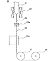
- FIG. 2 is a schematic diagram of a manufacturing apparatus 20 used in the method for manufacturing a coated optical fiber according to this embodiment.
- the manufacturing apparatus 20 is an apparatus for manufacturing a coated optical fiber by a wet-on-wet method.
- the optical fiber preform 21 is made of, for example, quartz glass and is manufactured by a known method such as a VAD method, an OVD method, or a CVD method.
- the end of the optical fiber preform 21 is heated and melted by a heater 22 disposed around the optical fiber preform 21, and drawn to draw the glass optical fiber 23 (that is, the glass optical fiber 11 in FIG. 1). It is.
- a resin coating device 24 a that applies an ultraviolet curable resin to the outer periphery of the glass optical fiber 23 is provided below the heater 22, a resin coating device 24 a that applies an ultraviolet curable resin to the outer periphery of the glass optical fiber 23 is provided.
- the resin coating device 24a separately holds an ultraviolet curable resin for the primary layer 12 (also referred to as primary ultraviolet curable resin) and an ultraviolet curable resin for the secondary layer 13 (also referred to as secondary ultraviolet curable resin).
- the glass optical fiber 23 drawn from the optical fiber preform 21 is applied with the primary UV curable resin and the secondary UV curable resin all at once by the resin coating device 24a.
- an ultraviolet irradiation unit 26a for irradiating the glass optical fiber 25 coated with the primary ultraviolet curable resin and the secondary ultraviolet curable resin is provided below the resin coating device 24a.
- the glass optical fiber 25 coated with the ultraviolet curable resin by the resin coating device 24a enters the ultraviolet irradiation unit 26a and is irradiated with ultraviolet rays emitted from the semiconductor light emitting element.
- the two layers of ultraviolet curable resin coated on the outer periphery of the glass optical fiber 25 are cured, and the two layers of ultraviolet curable resin become the primary layer 12 and the secondary layer 13.
- the glass optical fiber (that is, the coated optical fiber 10) in which the primary layer 12 and the secondary layer 13 are formed on the outer periphery is guided by the guide roller 27 and wound by the winding device 28.
- the ultraviolet irradiation unit 26a includes a unit in which one or a plurality of semiconductor light emitting elements that output ultraviolet rays in a narrow wavelength region having a peak wavelength from 300 nm to 405 nm, for example, are arranged.
- the irradiation energy is preferably 10mJ / cm 2 ⁇ 3000mJ / cm 2 from the viewpoint of thermal damage reduction to fast-curing resin, 30mJ / cm 2 ⁇ 1500mJ / cm 2 is more preferable.
- the semiconductor light emitting element is electrically connected to a control device (not shown) and its output is controlled.
- a light emitting diode (LED) is used as the semiconductor light emitting element, but any light emitting element capable of outputting ultraviolet rays of a predetermined wavelength using a semiconductor, such as a semiconductor laser, may be used.
- the high-pressure mercury lamp or the like When a high-pressure mercury lamp or the like is used as an ultraviolet light source as in a conventional coated optical fiber manufacturing apparatus, the high-pressure mercury lamp or the like has a plurality of peak wavelengths in the ultraviolet region and outputs ultraviolet rays in a wide wavelength region. Therefore, even if the absorption wavelengths of the photopolymerization initiators of the primary layer 12 and the secondary layer 13 partially overlap, a photopolymerization initiator whose absorption wavelength region is shifted between the primary layer 12 and the secondary layer 13 is used (for example, By making the absorption wavelength of the photopolymerization initiator of the primary layer 12 longer than that of the secondary layer 13, both the primary layer 12 and the secondary layer 13 can be sufficiently cured.
- FIG. 4 is a diagram schematically showing a change in the amount of light when the ultraviolet curable resin is irradiated with ultraviolet rays from a high-pressure mercury lamp or the like.
- the ultraviolet curable resin in FIG. 4 is a combination of the outer secondary layer 13 that absorbs less light at the long wavelength and the inner primary layer 12 that absorbs at the long wavelength side.
- the upper graph in FIG. 4 represents the absorbance of the secondary layer 13, and the lower graph in FIG. 4 represents the absorbance of the primary layer 12.
- the horizontal axis of each graph is wavelength (nm), and the vertical axis is absorbance (no unit).
- ultraviolet rays from an ultraviolet light source are indicated by arrows, and the amount of light (light intensity) increases as the number of arrows increases.
- the secondary layer 13 is irradiated with ultraviolet rays in a wide wavelength region from a high-pressure mercury lamp or the like.
- ultraviolet light in the low wavelength region is mainly absorbed by the outer secondary layer 13, and therefore, the inner primary layer 12 is mainly irradiated with ultraviolet light in the high wavelength region.
- ultraviolet rays from a high-pressure mercury lamp or the like are distributed over a wide wavelength region, a large amount of ultraviolet rays reaches the primary layer 12 even after being absorbed by the secondary layer 13, and the primary layer 12 is sufficiently cured. be able to.
- an ultraviolet semiconductor as an ultraviolet light source as in the coated optical fiber manufacturing apparatus described in Patent Documents 1 and 2
- the ultraviolet semiconductor light emitting element since the ultraviolet semiconductor light emitting element emits only a single wavelength (narrow wavelength region) of ultraviolet light, both the primary layer 12 and the secondary layer 13 may not be sufficiently cured.
- the secondary layer has the same level of elasticity as the conventional layer. The rate cannot be demonstrated.
- FIG. 5 is a diagram schematically showing a change in light quantity when the ultraviolet curable resin is irradiated with ultraviolet rays from the ultraviolet semiconductor light emitting element.
- the ultraviolet curable resin in FIG. 5 is obtained by combining the secondary layer 13 that does not contain a photopolymerization initiator corresponding to the wavelength region of the ultraviolet light from the ultraviolet semiconductor light emitting element, with the primary layer 12 similar to FIG.
- the definition of the information represented in the graph of FIG. 5 is the same as that of the graph of FIG.
- the secondary layer 13 is irradiated with ultraviolet rays in a narrow wavelength region from the ultraviolet semiconductor light emitting element.
- the outer secondary layer 13 does not contain much photo-polymerization initiator corresponding to the wavelength region of the ultraviolet light from the ultraviolet semiconductor light-emitting element, and therefore does not absorb much ultraviolet light. Therefore, as shown in the lower graph of FIG. 5, the inner primary layer 12 is irradiated with a large amount of ultraviolet rays. As a result, the primary layer 12 is cured, but the secondary layer 13 is not sufficiently cured.
- the primary Sufficient light may not be transmitted to the layer 12, and only the secondary layer 13 may be cured, and the curability of the primary layer 12 may be reduced.
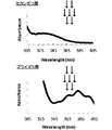
- FIG. 6 is a diagram schematically showing a change in light amount when the ultraviolet curable resin is irradiated with ultraviolet rays from the ultraviolet semiconductor light emitting element.
- the ultraviolet curable resin in FIG. 6 is obtained by combining the secondary layer 13 containing a photopolymerization initiator corresponding to the wavelength region of the ultraviolet light from the ultraviolet semiconductor light emitting element into the primary layer 12 similar to FIG.
- the definition of the information represented in the graph of FIG. 6 is the same as that of the graph of FIG.
- the secondary layer 13 is irradiated with ultraviolet rays in a narrow wavelength region from the ultraviolet semiconductor light emitting element.
- the outer secondary layer 13 contains a photopolymerization initiator corresponding to the wavelength region of the ultraviolet light from the ultraviolet semiconductor light-emitting element, and thus absorbs the ultraviolet light greatly. Therefore, as shown in the lower graph of FIG. 6, the amount of ultraviolet light applied to the inner primary layer 12 is significantly reduced. As a result, the secondary layer 13 is cured, but the primary layer 12 is not sufficiently cured.
- both the primary layer 12 and the secondary layer 13 are sufficiently cured even if the photocuring initiator corresponding to the wavelength region of the ultraviolet light from the ultraviolet semiconductor light emitting element is simply contained in the ultraviolet curable resin. It is difficult to let
- the secondary layer 13 and the secondary layer 13 have sufficient curability even when the wet-on-wet method is used.
- the photopolymerization initiator compounded in the ultraviolet curable resin used in the above process absorbs light in the wavelength region (350 nm to 405 nm in this embodiment) emitted from the light source of the ultraviolet semiconductor light emitting device, generates radicals, and is photobleached. It is comprised so that it may have squeezing property.
- the photopolymerization initiator blended in the primary layer 12 absorbs the same or similar wavelength region as that of the secondary layer 13 (350 nm to 405 nm in this embodiment).
- photobleaching is written as photobleaching; photobleaching and photobleaching. It is one of the environmental effects and refers to the photochemical properties rarely seen in excited fluorescent molecules. This reaction occurs because the fluorescent substance in the excited state is chemically activated and unstable compared to the ground state. As a result of this reaction, it means that the fluorescent molecule eventually changes to a low fluorescent structure.
- the photopolymerization initiator absorbs light in a certain ultraviolet region and generates radicals to initiate polymerization in the ultraviolet curable resin
- the photopolymerization initiator molecule conjugates after radical generation. That the bond is broken and the absorbance in the ultraviolet region decreases is called photobleaching.
- light in the ultraviolet region can be transmitted to the inside, so that even a thick film can be cured smoothly, and the primary layer 12 located inside the secondary layer 13 is sufficiently cured. be able to.
- FIG. 7 is a graph schematically showing a change in absorbance due to ultraviolet irradiation in an ultraviolet curable resin containing a photopolymerization initiator having photobleaching properties.
- FIG. 7 shows the absorbance of the UV curable resin having a thickness of 100 ⁇ m containing a photopolymerization initiator having photobleaching properties, the absorbance after 0 seconds, 10 seconds, and 30 seconds after the start of UV irradiation.
- a graph is represented.
- the absorbance is large in the wavelength region of 350 nm to 405 nm immediately after the ultraviolet irradiation (after 0 seconds)
- the absorbance in the wavelength region is 10 seconds after starting the ultraviolet irradiation and after 30 seconds. Is greatly reduced.
- the secondary layer 13 is cured, and a sufficient amount of ultraviolet light is supplied to the primary layer 12 inside the secondary layer 13. Can be cured.
- an ultraviolet curable resin having a thickness of 100 ⁇ m is used.
- the secondary layer 13 in an actual optical fiber has a thickness of about 10 ⁇ m to 50 ⁇ m, photobleaching is performed in a shorter time than shown in FIG. Sex is demonstrated. Therefore, the primary layer 12 and the secondary layer 13 can be cured within a period in which the optical fiber passes through the ultraviolet irradiation unit 26a of FIG.
- FIG. 8 is a graph schematically showing a change in light amount when the ultraviolet curable resin is irradiated with ultraviolet rays from an ultraviolet semiconductor light emitting element.
- the ultraviolet curable resin in FIG. 8 corresponds to the wavelength region of the ultraviolet light from the ultraviolet semiconductor light emitting element, and the secondary layer 13 containing a photopolymerization initiator having photobleaching properties is combined with the primary layer 12 similar to FIG. Is.
- the definition of the information represented in the graph of FIG. 8 is the same as that of the graph of FIG.
- the upper graph in FIG. 8 shows absorbance graphs after 0 seconds, 10 seconds, and 30 seconds after the start of ultraviolet irradiation.
- the secondary layer 13 is irradiated with ultraviolet rays in a narrow wavelength region from the ultraviolet semiconductor light emitting element.
- the photopolymerization initiator contained in the secondary layer 13 has photobleaching properties, and thus the absorbance of the secondary layer 13 decreases with time (that is, with the progress of curing). Therefore, as shown in the lower graph of FIG. 8, a large amount of ultraviolet light is irradiated to the inner primary layer 12 after a predetermined time has elapsed. As a result, both the primary layer 12 and the secondary layer 13 can be sufficiently cured.
- an acylphosphine oxide-based initiator can be used.
- 2,4,6-trimethylbenzoyl diphenylphosphine oxide (trade name: Lucirin (registered trademark, hereinafter abbreviated) TPO, BASF (registered trademark, abbreviated) Japan Ltd.), phenyl (2,4,6-trimethylbenzoyl) ) -Ethyl phosphinate (trade name: Lucirin TPO-L, BASF Japan Ltd.), bis (2,4,6-trimethylbenzoyl) -phenylphosphine oxide (trade name: Irgacure (registered trademark, hereinafter omitted) 819, Irgacure 819DW, BASF Japan Ltd.), bis (2,6-dimethoxybenzoyl) -2,4,4-trimethyl-pentylphosphine oxide (trade name: Irgacure 1700, BASF Japan
- two or more kinds of photopolymerization initiators may be used in combination.
- at least one of the above-described acylphosphine oxide type and O-acyloxime type photopolymerization initiators may include ⁇ It is preferable to use a combination of a -hydroxyalkylphenone type photopolymerization initiator. By combining these, the surface curability can be improved.
- the surface is further increased. Curability can be improved.
- the addition amount of the photopolymerization initiator having photobleaching properties is desirably 10 wt% or less with respect to the ultraviolet curable resin used for the secondary layer 13. If the amount is more than this, light may not reach the primary layer 12 sufficiently, or the secondary layer 13 may be colored.
- the photopolymerization initiator used in the present embodiment has an absorbance value at 365 nm of an ultraviolet curable resin containing the photopolymerization initiator of 80% or less, more preferably 50% of the value before curing when cured by irradiation with ultraviolet rays of 200 mJ. Photobleaching properties as described below are desirable for obtaining sufficient curability of the primary layer 12.
- the primary layer 12 having sufficient curability means a state in which the primary layer 12 has an elastic modulus of 0.2 MPa or more, more preferably 0.3 MPa or more after curing.
- the secondary layer 13 having sufficient curability means a state in which the secondary layer 13 has an elastic modulus of 500 MPa or more, more preferably 800 MPa or more after curing.
- the elastic modulus after curing of the primary layer 12 is 0.2 MPa or more and 3.0 MPa or less, more preferably 0.3 MPa or more and 1.5 MPa or less. Is preferred.
- the elastic modulus after hardening of the secondary layer 13 is 500 MPa or more and 2500 MPa or less, More preferably, it is 800 MPa or more and 2200 MPa or less.
- the absorption wavelength of the photopolymerization initiator used for the secondary layer 13 corresponds to the wavelength region of ultraviolet light output from the ultraviolet semiconductor light-emitting element, and the photopolymerization initiator is photobleached. It has the ability to That is, the secondary layer 13 is a photopolymerization initiator that generates radicals by absorbing light in a wavelength region (specifically, 350 nm to 405 nm) emitted from the ultraviolet semiconductor light emitting element, and is a photobleaching light. Contains a polymerization initiator.
- Example 1 A sample simulating a state in which two layers of a primary layer 12 and a secondary layer 13 were formed on a glass optical fiber was prepared, and the curability (elastic modulus) was measured.
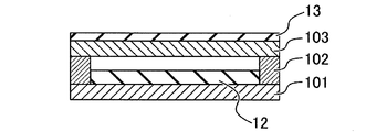
- Two quartz glasses were prepared. One of the quartz glasses 101 was spin-coated with a primary ultraviolet curable resin (100 ⁇ m), and the other quartz glass 103 was spin-coated with a secondary ultraviolet curable resin (50 ⁇ m).
- a spacer 102 (thickness 1 mm) is placed on a quartz glass 101 coated with a primary ultraviolet curable resin, and a quartz glass 103 coated with a secondary ultraviolet curable resin is placed thereon, and this is sampled. It was.
- the reason why the spacer is provided in this way is to prevent the primary ultraviolet curable resin from being in close contact with the quartz glass coated with the secondary ultraviolet curable resin and being destroyed when taken out.
- the prepared sample was put in a purge box to make a nitrogen atmosphere, the illuminance and speed were adjusted so as to obtain a predetermined integrated light amount by a conveyor type ultraviolet irradiation device, and ultraviolet rays (365 nm) were irradiated to cure the resin.
- the films made of the primary UV curable resin (primary layer 12) and the secondary UV curable resin (secondary layer 13) thus obtained were peeled off from the glass substrate, cut into 6 mm width strips, 2.5% modulus (elastic modulus) was measured according to JIS K 7161. As a result of this measurement, Table 1 shows the relationship between the types of the photopolymerization initiator and the light source and the curability of the primary layer 12 and the secondary layer 13.
- a photopolymerization initiator that absorbs light of 365 nm or more was used for the primary ultraviolet curable resin.
- the initiator for the secondary ultraviolet curable resin the following ones manufactured by BASF Japan Ltd. were used.
- Lucirin TPO, Irgacure 819 and Irgacure OXE01 are photopolymerization initiators having photobleaching properties, and other photopolymerization initiators having no photobleaching properties.
- D-bulb is a high-pressure mercury lamp
- 365 nm LED means an ultraviolet semiconductor light emitting device having a central wavelength of the light source wavelength of 365 nm.
- No. 1 uses a D-bulb which is a high-pressure mercury lamp as a light source, and both the secondary layer 13 and the primary layer 12 are sufficiently cured. However, no.
- a D-bulb which is a high-pressure mercury lamp as a light source
- both the secondary layer 13 and the primary layer 12 are sufficiently cured.
- the elastic modulus of the secondary layer 13 is less than 500 MPa. Insufficient curing.
- the absorption wavelength of the photopolymerization initiator of the secondary layer 13 is adjusted to the light source wavelength of the ultraviolet semiconductor light emitting element as in 3 and 4, light of the absorption wavelength of the photopolymerization initiator of the secondary layer 13 is transmitted to the primary layer 12.
- the elastic modulus of the primary layer 12 is less than 0.2 MPa, and the curing is insufficient.
- the photopolymerization initiator used for the secondary layer 13 in 5, 6, and 7 has an absorption wavelength corresponding to the light source wavelength of the ultraviolet semiconductor light-emitting element and has photobleaching properties.
- the elastic modulus of the secondary layer 13 was 500 MPa or more and the elastic modulus of the primary layer 12 was 0.2 MPa or more, and both the secondary layer 13 and the primary layer 12 showed good curability.
- no. 7 has high curability of the secondary layer 13.
- the photopolymerization initiator used in 8 mainly absorbs the light source wavelength of the ultraviolet semiconductor light emitting device, but does not have photobleaching properties. Therefore, although excellent curability of the secondary layer 13 is brought about, since there is no photobleaching property, ultraviolet rays do not reach the inside, and the elastic modulus of the primary layer 12 is less than 0.2 MPa, resulting in insufficient curing.
- the secondary layer 13 using this photopolymerization initiator is suitable for the wet-on-dry system in which the light source is an ultraviolet semiconductor light emitting element.
- No. 9 has a photopolymerization initiator having an absorption wavelength corresponding to the light source wavelength of the ultraviolet semiconductor light-emitting element and having photobleaching properties, and a surface curability having no absorption peak in the light source wavelength region of the ultraviolet semiconductor light-emitting element.
- An excellent photopolymerization initiator was used in the secondary layer 13 together.
- the elastic modulus of the secondary layer 13 is 500 MPa or more
- the elastic modulus of the primary layer 12 is 0.2 MPa or more
- both the secondary layer 13 and the primary layer 12 exhibit good curability and good surface curability. can get.
- an optical fiber having a coating resin with a high elastic modulus can be obtained. There is an effect.
Landscapes
- Life Sciences & Earth Sciences (AREA)
- Physics & Mathematics (AREA)
- Chemical & Material Sciences (AREA)
- Engineering & Computer Science (AREA)
- Chemical Kinetics & Catalysis (AREA)
- General Chemical & Material Sciences (AREA)
- Geochemistry & Mineralogy (AREA)
- Materials Engineering (AREA)
- Organic Chemistry (AREA)
- General Life Sciences & Earth Sciences (AREA)
- General Physics & Mathematics (AREA)
- Optics & Photonics (AREA)
- Surface Treatment Of Glass Fibres Or Filaments (AREA)
- Optical Fibers, Optical Fiber Cores, And Optical Fiber Bundles (AREA)
Abstract
本発明は、樹脂硬化用の光源として紫外線半導体発光素子を用い、Wet-on-Wet方式でガラス光ファイバに樹脂を被覆する場合でも、高い弾性率の被覆層を有する被覆光ファイバおよび被覆光ファイバの製造方法を提供する。本発明の一実施形態に係る被覆光ファイバ10の製造方法は、ガラス光ファイバ11に第1の紫外線硬化樹脂12を塗布する工程と、第1の紫外線硬化樹脂を硬化させる前に、第1の紫外線硬化樹脂の外周に第2の紫外線硬化樹脂13を塗布する工程と、第1および第2の紫外線硬化樹脂に対して紫外線半導体発光素子より発せられる350nm~405nmの波長領域の光を照射する工程と、を備え、第2の紫外線硬化樹脂は、紫外線半導体発光素子からの光を吸収してラジカルを発生する光重合開始剤を含有し、光重合開始剤はフォトブリーチング性を有する。
Description
本発明は、プライマリ層とセカンダリ層とにより被覆された被覆光ファイバ、および被覆光ファイバの製造方法に関する。
被覆光ファイバは、一般的に、プリフォーム(光ファイバ母材とも称される)から線引きされたガラス光ファイバの表面に樹脂を被覆することによって製造される。被覆は、まずガラス光ファイバの外周に紫外線硬化樹脂を塗布し、その紫外線硬化樹脂に紫外線(UV光)を照射して硬化させることによって形成される。紫外線硬化樹脂は、光ファイバ被覆以外にも様々な工業分野で使われている。例えば塗料や印刷インキの硬化や、電子回路をはじめとして様々な製品の保護コーティング用にも使用される。一般的に、紫外線硬化樹脂は約200nm~400nmの波長の紫外線が照射されることで短時間に効率的に硬化する。
従来、光ファイバ被覆硬化装置(被覆光ファイバ製造装置)のUV光の光源としては高圧水銀ランプやメタルハライドランプ(以下、高圧水銀ランプ等と記載する)が用いられている。高圧水銀ランプは、石英ガラス製の発光管の中に高純度の水銀(Hg)と少量の希ガスが封入されたもので、365nmを主波長とし、254nm、303nm、313nmの紫外線を効率よく放射する。また、同様に用いられているメタルハライドランプは、発光管の中に水銀に加えて金属をハロゲン化物の形で封入したもので、200nm~450nmまで広範囲にわたり紫外線スペクトルを放射している。
ガラス光ファイバに紫外線硬化樹脂を被覆する方法としては、Wet-on-Wet方式と、Wet-on-Dry方式とが知られている。Wet-on-Wet方式は、複数の紫外線硬化樹脂層をガラス光ファイバ上に塗布してから紫外線を照射することにより、該複数の紫外線硬化樹脂層を一度の紫外線照射によってまとめて硬化させる方法である。一方、Wet-on-Dry方式は、単一の紫外線樹脂層をガラス光ファイバ上に塗布し、該単一の紫外線樹脂層に対して紫外線を照射して硬化させ、さらにその上に紫外線樹脂層の塗布および紫外線の照射を行う方法である。
光ファイバの製造工程で用いられる、複数の樹脂を塗布した後に硬化させるWet-on-Wet方式では、上記約200nm~400nmの波長の紫外線で複数の被覆層を効率的に硬化させるため、例えば、上層のセカンダリ層には約200nm~350nmの紫外線を吸収する光重合開始剤、下層のプライマリ層には約200nm~350nm及び350nm以上の紫外線を吸収する光重合開始剤が添加される。これにより、上記の高圧水銀ランプ等による紫外線照射により、それぞれの被覆層が十分に紫外線を吸収して、硬化する。
近年、紫外線硬化樹脂を硬化させるときの消費電力を低減させるため、従来の高圧水銀ランプ等に代えて、UV光の光源として紫外線レーザダイオード(UV-LD)または紫外線発光ダイオード(UV-LED)などの紫外線半導体発光素子を光源として使用する試みがなされている。
例えば、特許文献1には、紫外線照射ユニット内部に、紫外線を側面から出射可能な導光路と、紫外線光源である半導体発光素子と、を備えた紫外線照射装置が開示されている。この装置によれば、導光路内部に導入された紫外線を、導光路の側面から被覆樹脂に対してライン状に出射することができるので、数少ない紫外線光源を用いた場合においても十分な積算光量を得ることでき、被覆樹脂の硬化性及び装置寿命を向上できるとされている。
また、特許文献2には、広い波長域を有する高圧水銀ランプ等と比較して、単一波長を有する半導体発光素子を樹脂硬化光源に用いる場合、紫外線硬化樹脂組成物に、半導体発光素子の出射光波長に吸収領域を有する光重合開始剤を含有させたものを被覆樹脂として用いることによって、被覆樹脂の硬化性を向上させる方法が開示されている。
しかしながら、複数の紫外線硬化樹脂層を塗布した後に一括で硬化させるWet-on-Wet方式において半導体発光素子を光源として用いる場合、特許文献2のように紫外線半導体発光素子の出射光波長に吸収領域を有する光重合開始剤を含有する紫外線硬化樹脂を用いたとしても、高圧水銀ランプ等を使用した場合と同レベルまで紫外線硬化樹脂を硬化させて、同レベルの弾性率(ヤング率)を有する被覆層が得られない場合があることが分かった。
従来の高圧水銀ランプ等の光源に代わり、LED等の半導体発光素子を光源に用いる場合、プライマリ層およびセカンダリ層を含む複数層を硬化するためには、少なくとも200nm~350nmと350nm以上との2つの波長領域に紫外線を照射する必要がある。
しかし、現在製品化されている高出力な半導体発光素子光源は365nm~405nm波長域で1000mW/cm2以上の出力が期待できるが、現在製品化されている200nm~350nmの深紫外域の紫外線を出力する半導体発光素子の出力は1mW/cm2~10mW/cm2であり、365nm以上の波長を出力する半導体発光素子光源と比較すると大幅に低出力である。よって、一般的な半導体発光素子を用いて、少なくとも200nm~350nmと350nm以上との2つの波長領域において光ファイバ被覆樹脂の硬化に十分な出力を有する紫外光を照射することは難しい。
そこで、本発明は、樹脂硬化用の光源として紫外線半導体発光素子を用い、Wet-on-Wet方式でガラス光ファイバに樹脂を被覆する場合でも、高い弾性率の被覆層を有する被覆光ファイバおよび被覆光ファイバの製造方法を提供することを目的とする。
本発明の一態様に係る被覆光ファイバの製造方法は、ガラス光ファイバと、前記ガラス光ファイバを被覆するプライマリ層と、前記プライマリ層を被覆するセカンダリ層とを有する被覆光ファイバの製造方法であって、前記ガラス光ファイバに第1の紫外線硬化樹脂を塗布する工程と、前記第1の紫外線硬化樹脂を硬化させる前に、前記第1の紫外線硬化樹脂の外周に第2の紫外線硬化樹脂を塗布する工程と、前記第1の紫外線硬化樹脂および前記第2の紫外線硬化樹脂に対して紫外線半導体発光素子より発せられる350~405nmの波長領域の光を照射することによって、前記プライマリ層および前記セカンダリ層を形成する工程と、を備え、前記第2の紫外線硬化樹脂は、前記紫外線半導体発光素子からの前記光を吸収してラジカルを発生する光重合開始剤を含有し、前記光重合開始剤はフォトブリーチング性を有することを特徴とする。
本発明の一態様に係る被覆光ファイバは、ガラス光ファイバと、前記ガラス光ファイバを被覆するプライマリ層と、前記プライマリ層を被覆するセカンダリ層と、を備え、前記セカンダリ層は、紫外線半導体発光素子より発せられる350~405nmの波長領域の光を吸収してラジカルを発生する光重合開始剤を含有する紫外線硬化樹脂に対して、前記紫外線半導体発光素子からの前記光を照射することによって形成され、前記光重合開始剤はフォトブリーチング性を有し、前記プライマリ層の弾性率が0.2MPa以上3.0MPa以下であり、前記セカンダリ層の弾性率が500MPa以上2000MPa以下であることを特徴とする。
本発明によれば、第1の紫外線硬化樹脂の外周に被覆される第2の紫外線硬化樹脂がフォトブリーチング性を有する光重合開始剤を含有するため、第2の紫外線硬化樹脂だけでなく第1の紫外線硬化樹脂にも大きな光量の紫外線が到達できる。そのため、第1および第2の紫外線硬化樹脂が未硬化の状態で紫外線を照射するWet-on-Wet方式であっても、第1および第2の紫外線硬化樹脂の両方の硬化性を高めることができる。
以下、図面を参照して、本発明の実施の形態を説明するが、本発明は本実施形態に限定されるものではない。なお、以下で説明する図面で、同機能を有するものは同一符号を付け、その繰り返しの説明は省略することもある。
(実施形態)
図1は、本実施形態に係る被覆光ファイバの概略断面図を示す。図1に示すように、被覆光ファイバ10は、ガラス光ファイバ11と、ガラス光ファイバ11の外周に被覆された軟質層であるプライマリ層12および硬質層であるセカンダリ層13からなる2層の被覆層14とを有する。プライマリ層12およびセカンダリ層13は、紫外線硬化樹脂に紫外線を照射して硬化されてなる被覆樹脂からなり、ガラス光ファイバ11を保護する機能を有している。被覆光ファイバ10の構成はこの構成に限定されず、被覆層14は3層以上の層を含んでよく、また被覆層14の外周は着色された着色層や、複数の被覆光ファイバ10を束ねる一括被覆層等によりさらに被覆されてよい。
図1は、本実施形態に係る被覆光ファイバの概略断面図を示す。図1に示すように、被覆光ファイバ10は、ガラス光ファイバ11と、ガラス光ファイバ11の外周に被覆された軟質層であるプライマリ層12および硬質層であるセカンダリ層13からなる2層の被覆層14とを有する。プライマリ層12およびセカンダリ層13は、紫外線硬化樹脂に紫外線を照射して硬化されてなる被覆樹脂からなり、ガラス光ファイバ11を保護する機能を有している。被覆光ファイバ10の構成はこの構成に限定されず、被覆層14は3層以上の層を含んでよく、また被覆層14の外周は着色された着色層や、複数の被覆光ファイバ10を束ねる一括被覆層等によりさらに被覆されてよい。
ガラス光ファイバ11の直径は、通常100μm~150μmであり、124μm~126μmが一般的である。プライマリ層12の厚さは、通常10μm~50μmであり、セカンダリ層13の厚さは、通常10μm~50μmである。また、被覆光ファイバ10の直径(すなわち、セカンダリ層13の外径)は、通常245μm~255μmである。
光ファイバの被覆樹脂として用いる紫外線硬化樹脂は、例えば、紫外線で重合・硬化するエチレン性不飽和基を少なくとも2つ有する紫外線硬化樹脂を使用し、好ましくはオリゴマーを使用する。なお、ここでオリゴマーとは、重合度が2~100の重合体である。また、該紫外線硬化樹脂は、後述する所定の性質を有する光重合開始剤を含む。
該紫外線硬化樹脂は、オリゴマーおよび光重合開始剤に加えて、希釈モノマー、光増感剤、シランカップリング剤、連鎖移動剤および各種添加剤を含んでもよい。希釈モノマーとしては、単官能(メタ)アクリレートまたは多官能(メタ)アクリレートが用いられる。希釈モノマーとは、紫外線硬化樹脂を希釈するためのモノマーを意味する。
図2は、本実施形態に係る被覆光ファイバの製造方法に用いる製造装置20の概略模式図である。製造装置20は、Wet-on-Wet方式で被覆光ファイバを製造する装置である。
光ファイバ母材21は、例えば石英系のガラスからなり、VAD法、OVD法、CVD法など周知の方法で製造される。光ファイバ母材21の端部は、光ファイバ母材21の周囲に配置されたヒータ22によって加熱されて溶融し、線引きされてガラス光ファイバ23(すなわち、図1のガラス光ファイバ11)が引き出される。
ヒータ22の下方には、ガラス光ファイバ23の外周に紫外線硬化樹脂を塗布する樹脂塗布装置24aが設けられる。樹脂塗布装置24aには、プライマリ層12用の紫外線硬化樹脂(プライマリ用紫外線硬化樹脂ともいう)とセカンダリ層13用の紫外線硬化樹脂(セカンダリ用紫外線硬化樹脂ともいう)とが別々に保持される。光ファイバ母材21から引き出されたガラス光ファイバ23は、樹脂塗布装置24aによってプライマリ用紫外線硬化樹脂とセカンダリ用紫外線硬化樹脂とが一括して塗布される。
樹脂塗布装置24aの下方には、プライマリ用紫外線硬化樹脂およびセカンダリ用紫外線硬化樹脂が被覆されたガラス光ファイバ25に対して紫外線を照射する紫外線照射ユニット26aが設けられる。樹脂塗布装置24aによって紫外線硬化樹脂が塗布されたガラス光ファイバ25は、紫外線照射ユニット26aに入り、半導体発光素子から発せられる紫外線が照射される。その結果、ガラス光ファイバ25の外周に被覆された2層の紫外線硬化樹脂は硬化され、該2層の紫外線硬化樹脂はプライマリ層12とセカンダリ層13となる。
外周にプライマリ層12とセカンダリ層13が形成されたガラス光ファイバ(すなわち、被覆光ファイバ10)は、ガイドローラ27にガイドされ、巻取り装置28に巻き取られる。
紫外線照射ユニット26aは、例えば300nmから405nmにピーク波長を有する狭い波長領域の紫外線を出力する半導体発光素子が、一または複数個配設されてなるものを備える。照射エネルギーは、高速硬化と樹脂への熱ダメージ軽減の観点から10mJ/cm2~3000mJ/cm2が好ましく、30mJ/cm2~1500mJ/cm2がより好ましい。半導体発光素子は、制御装置(図示せず)に電気的に接続され、その出力が制御される。本実施形態では半導体発光素子として発光ダイオード(LED)を用いるが、半導体を利用して所定波長の紫外線を出力可能な任意の発光素子、例えば半導体レーザ等を用いてもよい。
ここで、従来技術と本実施形態に係る発明を対比して、被覆樹脂に照射する紫外線と光重合開始剤との関係について説明する。
従来の被覆光ファイバ製造装置のように紫外線光源として高圧水銀ランプ等を用いた場合、高圧水銀ランプ等は紫外域に複数のピーク波長を有しており、広い波長領域の紫外線を出力する。そのため、仮にプライマリ層12とセカンダリ層13の光重合開始剤の吸収波長が一部重なっても、プライマリ層12とセカンダリ層13とで吸収波長領域がずれている光重合開始剤を用いる(例えば、プライマリ層12の光重合開始剤の吸収波長がセカンダリ層13のそれよりも長波長側である)ことによって、プライマリ層12とセカンダリ層13の両方を充分に硬化させることができる。
図4は、高圧水銀ランプ等からの紫外線を紫外線硬化樹脂に照射する場合の光量変化を模式的に表すグラフを示す図である。図4における紫外線硬化樹脂は、長波長に吸収が少ない外側のセカンダリ層13と、長波長側に吸収を持つ内側のプライマリ層12とを組み合わせたものである。図4の上のグラフはセカンダリ層13の吸光度を表し、図4の下のグラフはプライマリ層12の吸光度を表す。各グラフの横軸は波長(nm)であり、縦軸は吸光度(無単位)である。各グラフには紫外線光源からの紫外線が矢印で示されており、矢印の数が多いほど光量(光強度)が大きいことを示す。
図4の上のグラフに示すように、セカンダリ層13には高圧水銀ランプ等から広い波長領域の紫外線が照射される。また、図4の下のグラフに示すように、外側のセカンダリ層13によって主に低波長領域の紫外線が吸収されるため、内側のプライマリ層12には高波長領域の紫外線が主に照射される。しかしながら、高圧水銀ランプ等からの紫外線は広い波長領域に分布するため、セカンダリ層13による吸収を受けた後もプライマリ層12に大きな光量の紫外線が到達しており、プライマリ層12は十分に硬化することができる。
一方、特にWet-on-Wet法においてプライマリ層12およびセカンダリ層13を塗布してから一括で硬化させる際に、特許文献1および2に記載の被覆光ファイバ製造装置のように紫外線光源として紫外線半導体発光素子を用いると、紫外線半導体発光素子が単波長(狭い波長領域)の紫外線しか発しないことから、プライマリ層12とセカンダリ層13の両方を充分に硬化させることができない場合がある。
具体的には、セカンダリ層に用いられる紫外線硬化樹脂が、紫外線半導体発光素子の光源波長(365nm~405nm)に対応した光重合開始剤を含んでいない場合は、セカンダリ層は従来と同レベルの弾性率を発揮できない。
図5は、紫外線半導体発光素子からの紫外線を紫外線硬化樹脂に照射する場合の光量変化を模式的に表すグラフを示す図である。図5における紫外線硬化樹脂は、紫外線半導体発光素子からの紫外線の波長領域に対応する光重合開始剤を含まないセカンダリ層13を図4と同様のプライマリ層12に組み合わせたものである。図5のグラフに表される情報の定義は、図4のグラフと同様である。
図5の上のグラフに示すように、セカンダリ層13には紫外線半導体発光素子から狭い波長領域の紫外線が照射される。図5の上のグラフからわかるように、外側のセカンダリ層13は、紫外線半導体発光素子からの紫外線の波長領域に対応する光重合開始剤を含まないため、紫外線をあまり吸収しない。そのため、図5の下のグラフに示すように、内側のプライマリ層12には大きい光量の紫外線が照射される。その結果、プライマリ層12は硬化するものの、セカンダリ層13は十分に硬化しない。
一方、特許文献2に記載の被覆光ファイバ製造装置のように、セカンダリ層13に用いられる紫外線硬化樹脂に紫外線半導体発光素子からの紫外線の波長領域に対応した光重合開始剤を含有させると、プライマリ層12に十分な光が伝わらず、セカンダリ層13のみが硬化し、プライマリ層12の硬化性が低下することがある。
図6は、紫外線半導体発光素子からの紫外線を紫外線硬化樹脂に照射する場合の光量変化を模式的に表すグラフを示す図である。図6における紫外線硬化樹脂は、紫外線半導体発光素子からの紫外線の波長領域に対応する光重合開始剤を含むセカンダリ層13を図4と同様のプライマリ層12に組み合わせたものである。図6のグラフに表される情報の定義は、図4のグラフと同様である。
図6の上のグラフに示すように、セカンダリ層13には紫外線半導体発光素子から狭い波長領域の紫外線が照射される。図6の上のグラフからわかるように、外側のセカンダリ層13は紫外線半導体発光素子からの紫外線の波長領域に対応する光重合開始剤を含むため、紫外線を大きく吸収する。そのため、図6の下のグラフに示すように、内側のプライマリ層12に照射される紫外線の光量は大幅に低下する。その結果、セカンダリ層13は硬化するものの、プライマリ層12は十分に硬化しない。
すなわち、図6からわかるように、紫外線硬化樹脂に単に紫外線半導体発光素子からの紫外線の波長領域に対応する光重合開始剤を含有させても、プライマリ層12およびセカンダリ層13の両方を十分に硬化させることは難しい。
それに対して、本実施形態に係る光ファイバ用被覆樹脂においては、Wet-on-Wet法を用いた場合でもプライマリ層12とセカンダリ層13が十分な硬化性を得るようにするため、セカンダリ層13に用いられる紫外線硬化樹脂に配合される光重合開始剤は、紫外線半導体発光素子の光源より発せられる波長領域(本実施形態では350nm~405nm)の光を吸収してラジカルを発生し、かつフォトブリーチング性を有するように構成される。プライマリ層12に配合される光重合開始剤は、セカンダリ層13と同じまたは近似する波長領域(本実施形態では350nm~405nm)を吸収するものである。
ここで、フォトブリーチングとは、photobleaching;光退色、光脱色とも書き、環境効果の一つで、励起蛍光分子でまれにみられる光化学的性質をさす。この反応は、励起状態にある蛍光物質が基底状態に比べて化学的に活性化され不安定になるために起こる。この反応の結果、蛍光分子が最終的に低蛍光性の構造に変化することを意味する。本実施形態に係る発明では、光重合開始剤がある紫外線領域において光を吸収し、ラジカルを発生させて紫外線硬化樹脂に重合を開始させる際に、ラジカル発生後の光重合開始剤の分子の共役結合が切断され、該紫外線領域における吸光度が低下することを、フォトブリーチングという。その結果、その紫外線領域における光を内部まで透過させることができるため、厚い膜であっても硬化をスムーズに進ませることができ、セカンダリ層13の内側に位置するプライマリ層12を充分に硬化させることができる。
図7は、フォトブリーチング性を有する光重合開始剤を含む紫外線硬化樹脂における紫外線照射による吸光度変化を模式的に表すグラフを示す図である。図7には、フォトブリーチング性を有する光重合開始剤を含む100μm厚の紫外線硬化樹脂に対して、紫外線の照射開始からの秒数が0秒後、10秒後、30秒後の吸光度のグラフが表されている。図7からわかるように、紫外線照射直後(0秒後)には特に350nm~405nmの波長領域で吸光度が大きいものの、紫外線を照射開始してから10秒後、30秒後には該波長領域の吸光度が大きく低下する。本実施形態では、このようなフォトブリーチング性を有する光重合開始剤を用いることによって、セカンダリ層13を硬化させるとともに、セカンダリ層13の内側にあるプライマリ層12に十分な光量の紫外線を供給して硬化させることができる。
なお、図7では100μm厚の紫外線硬化樹脂を用いているが、実際の光ファイバにおけるセカンダリ層13は10μm~50μm程度の厚さであるため、図7に示すよりもさらに短時間でフォトブリーチング性が発揮される。したがって、光ファイバが図2の紫外線照射ユニット26aを通過する期間内にプライマリ層12およびセカンダリ層13は硬化可能である。
図8は、紫外線半導体発光素子からの紫外線を紫外線硬化樹脂に照射する場合の光量変化を模式的に表すグラフを示す図である。図8における紫外線硬化樹脂は、紫外線半導体発光素子からの紫外線の波長領域に対応し、かつフォトブリーチング性を有する光重合開始剤を含むセカンダリ層13を図4と同様のプライマリ層12に組み合わせたものである。図8のグラフに表される情報の定義は、図4のグラフと同様である。また、図8の上のグラフには、紫外線の照射開始からの秒数が0秒後、10秒後、30秒後の吸光度のグラフが表されている。
図8の上のグラフに示すように、セカンダリ層13には紫外線半導体発光素子から狭い波長領域の紫外線が照射される。図8の上のグラフからわかるように、セカンダリ層13に含まれる光重合開始剤はフォトブリーチング性を有するため、セカンダリ層13の吸光度は時間経過とともに(すなわち、硬化の進行とともに)低下する。そのため、図8の下のグラフに示すように、所定の時間経過後には内側のプライマリ層12に大きい光量の紫外線が照射される。その結果、プライマリ層12およびセカンダリ層13は、共に十分に硬化することができる。
フォトブリーチング性を有する光重合開始剤としては、アシルホスフィンオキサイド系開始剤を用いることができる。例えば、2,4,6-トリメチルベンゾイルジフェニルホスフィンオキサイド(商品名:Lucirin(登録商標、以下省略)TPO、BASF(登録商標、以下省略)ジャパン株式会社)、フェニル(2,4,6-トリメチルベンゾイル)-ホスフィン酸エチル(商品名:LucirinTPO-L、BASFジャパン株式会社)、ビス(2,4,6-トリメチルベンゾイル)-フェニルホスフィンオキサイド(商品名:Irgacure(登録商標、以下省略)819、Irgacure819DW、BASFジャパン株式会社)、ビス(2,6-ジメトキシベンゾイル)-2,4,4-トリメチル-ペンチルホスフィンオキサイド(商品名:Irgacure1700、BASFジャパン株式会社)等を挙げることができる。さらに市販品として、Irgacure2100、Darocur4265、Irgacure2022(いずれもBASFジャパン株式会社)等を挙げことができる。
また、フォトブリーチング性を有する光重合開始剤として、O-アシルオキシム系開始剤である1-[4-(フェニルチオ)フェニル]-1,2-オクタンジオン2-(O-ベンゾイルオキシム)(商品名:IrgacureOXE01、BASFジャパン株式会社)を用いることができる。
本実施形態に係る発明では、光重合開始剤を2種以上組み合わせて使用してもよく、この場合、上述のアシルホスフィンオキサイド型およびO-アシルオキシム型の少なくとも一方の光重合開始剤に、α-ヒドロキシアルキルフェノン型の光重合開始剤を組み合わせて用いることが好ましい。これらを組み合わせることで表面硬化性を向上することができる。特にアシルホスフィンオキサイド型およびO-アシルオキシム型の光重合開始剤の少なくとも一方と、α-ヒドロキシアルキルフェノン型の光重合開始剤と、で異なる波長に吸収ピークを有するものを用いると、よりいっそう表面硬化性を向上することができる。
フォトブリーチング性を有する光重合開始剤の添加量は、セカンダリ層13に用いられる紫外線硬化樹脂に対して10wt%以下が望ましい。これ以上多いとプライマリ層12へ光が十分に届かなかったり、セカンダリ層13が着色したりする可能性がある。
また、本実施形態で用いる光重合開始剤は、それを含む紫外線硬化樹脂の365nmの吸光度の値が、紫外線200mJ照射により硬化させたときに硬化前の値の80%以下、より好ましくは50%以下になるようなフォトブリーチング性を有することが、プライマリ層12の十分な硬化性を得るためにも望ましい。
本実施形態においてプライマリ層12が十分な硬化性を有することとは、プライマリ層12が硬化後に0.2MPa以上、より好ましくは0.3MPa以上の弾性率を有する状態をいう。同様にセカンダリ層13が十分な硬化性を有することとは、セカンダリ層13が硬化後に500MPa以上、より好ましくは800MPa以上の弾性率を有する状態をいう。
なお、被覆光ファイバ10が特性および機能を保持するためには、プライマリ層12の硬化後の弾性率が0.2MPa以上3.0MPa以下、より好ましくは0.3MPa以上1.5MPa以下であることが好ましい。また、セカンダリ層13の硬化後の弾性率が500MPa以上2500MPa以下、より好ましくは800MPa以上2200MPa以下であることが好ましい。
なお、被覆光ファイバ10が特性および機能を保持するためには、プライマリ層12の硬化後の弾性率が0.2MPa以上3.0MPa以下、より好ましくは0.3MPa以上1.5MPa以下であることが好ましい。また、セカンダリ層13の硬化後の弾性率が500MPa以上2500MPa以下、より好ましくは800MPa以上2200MPa以下であることが好ましい。
本実施形態に係る発明においては、セカンダリ層13に使用する光重合開始剤の吸収波長は、紫外線半導体発光素子が出力する紫外線の波長領域に対応しており、かつ該光重合開始剤はフォトブリーチング性を有する。すなわち、セカンダリ層13は、紫外線半導体発光素子より発せられる波長領域(具体的には350nm~405nm)の光を吸収してラジカルを発生する光重合開始剤であって、フォトブリーチング性を有する光重合開始剤を含有する。
本実施形態に係る発明においては、単一波長または非常に狭い波長領域の紫外線を出力する半導体発光素子を光源として用いる場合であっても、セカンダリ層13に上述の所定の性質を有する光重合開始剤を含有させることによって、プライマリ層12およびセカンダリ層13の両方を十分に硬化させることができる。また、一般的に入手が容易な単一種類の半導体発光素子を用いることが可能であるため、安価に製造装置を構成することができる。
(実施例)
ガラス光ファイバにプライマリ層12とセカンダリ層13の2層を形成した状態を模擬したサンプルを作製し、硬化性(弾性率)の測定を行った。石英ガラスを2枚用意し、一方の石英ガラス101にプライマリ用紫外線硬化樹脂(100μm)をスピンコートし、もう一方の石英ガラス103にセカンダリ用紫外線硬化樹脂(50μm)をスピンコートした。
ガラス光ファイバにプライマリ層12とセカンダリ層13の2層を形成した状態を模擬したサンプルを作製し、硬化性(弾性率)の測定を行った。石英ガラスを2枚用意し、一方の石英ガラス101にプライマリ用紫外線硬化樹脂(100μm)をスピンコートし、もう一方の石英ガラス103にセカンダリ用紫外線硬化樹脂(50μm)をスピンコートした。
図3に示すようにプライマリ用紫外線硬化樹脂を塗布した石英ガラス101上にスペーサー102(厚さ1mm)を設置し、その上にセカンダリ用紫外線硬化樹脂を塗布した石英ガラス103を置き、これをサンプルとした。
このようにスペーサーを設ける理由は、プライマリ用紫外線硬化樹脂がセカンダリ用紫外線硬化樹脂を塗布した石英ガラスと密着して取り出しの際に破壊されるのを防止するためである。
作製したサンプルをパージボックスに入れ窒素雰囲気にし、コンベヤ型紫外線照射装置にて所定の積算光量になるように照度、速度を調整し、紫外線(365nm)照射し、樹脂を硬化した。
得られたプライマリ用紫外線硬化樹脂(プライマリ層12)、セカンダリ用紫外線硬化樹脂(セカンダリ層13)からなるフィルムをそれぞれガラス基材より剥がし、6mm幅の短冊状に切断して短冊状にし、それの2.5%モジュラス(弾性率)をJIS K 7161に準拠して測定した。この測定の結果として、表1は、光重合開始剤および光源の種類と、プライマリ層12およびセカンダリ層13の硬化性との関係を表す。
ここで、プライマリ用紫外線硬化樹脂には365nm以上の光を吸収する光重合開始剤を使用した。また、セカンダリ用紫外線硬化樹脂の開始剤としては、BASFジャパン株式会社製の以下のものを用いた。
No.1、No.2:Irgacure184(IC184)
No.3:Irgacure369(IC369)
No.4:Irgacure379(IC379)
No.5:LucirinTPO(TPO)
No.6:Irgacure819(819)
No.7:IrgacureOXE01(OXE01)
No.8:IrgacureOXE02(OXE02)
No.9:OXE01およびIC184
No.3:Irgacure369(IC369)
No.4:Irgacure379(IC379)
No.5:LucirinTPO(TPO)
No.6:Irgacure819(819)
No.7:IrgacureOXE01(OXE01)
No.8:IrgacureOXE02(OXE02)
No.9:OXE01およびIC184
上述のようにLucirinTPO、Irgacure819およびIrgacureOXE01はフォトブリーチング性を有する光重合開始剤であり、それ以外はフォトブリーチング性を有しない光重合開始剤である。
また、表1中のD-bulbは高圧水銀ランプであり、365nmLEDは光源波長の中心波長が365nmである紫外線半導体発光素子を意味する。
また、判定は、被覆光ファイバが特性および機能を保持できる、セカンダリ層13の弾性率が500MPa以上、かつプライマリ層12の弾性率が0.2MPa以上の場合に○とした。

No.1は光源として高圧水銀ランプであるD-bulbを用いており、セカンダリ層13、プライマリ層12の両方が充分硬化している。しかし、No.2のように光源として紫外線半導体発光素子を用いた場合であって、該紫外線半導体発光素子の光源波長をあまり吸収しない光重合開始剤を用いた場合は、セカンダリ層13の弾性率が500MPa未満となり硬化不足である。
一方、No.3、4のようにセカンダリ層13の光重合開始剤の吸収波長を紫外線半導体発光素子の光源波長に合わせた場合には、セカンダリ層13の光重合開始剤の吸収波長の光がプライマリ層12に届かず、プライマリ層12の弾性率が0.2MPa未満となり硬化不足である。
No.5、6、7でセカンダリ層13に使用した光重合開始剤は、吸収波長が紫外線半導体発光素子の光源波長に対応しており、かつフォトブリーチング性を有する。これらを用いた場合、セカンダリ層13の弾性率が500MPa以上、かつプライマリ層12の弾性率が0.2MPa以上となり、セカンダリ層13及びプライマリ層12が共に良好な硬化性を示した。特にNo.7は、セカンダリ層13の硬化性が高い。
No.8で使用した光重合開始剤は、紫外線半導体発光素子の光源波長を主に吸収するが、フォトブリーチング性を有しない。そのため、優れたセカンダリ層13の硬化性をもたらすが、フォトブリーチング性が無いため紫外線が内部まで到達せず、プライマリ層12の弾性率が0.2MPa未満となり硬化不足である。この光重合開始剤を使用したセカンダリ層13は光源を紫外線半導体発光素子としたWet-on-Dry方式に適している。
No.9では、吸収波長が紫外線半導体発光素子の光源波長に対応しており、かつフォトブリーチング性を有する光重合開始剤と、紫外線半導体発光素子の光源波長域に吸収ピークを持たない表面硬化性に優れる光重合開始剤とを、セカンダリ層13に併用した。この場合、セカンダリ層13の弾性率が500MPa以上、かつプライマリ層12の弾性率が0.2MPa以上となり、セカンダリ層13及びプライマリ層12が共に良好な硬化性を示すと共に、良好な表面硬化性が得られる。
本発明によれば、樹脂硬化用の光源として紫外線半導体発光素子を用い、Wet-on-Wet方式で被覆光ファイバを作製した場合でも、高い弾性率の被覆樹脂を有する光ファイバを得ることができるという効果を奏する。
本発明は上述の実施例に限定されることなく、本発明の趣旨を逸脱しない範囲において変更実施が可能である。
Claims (8)
- ガラス光ファイバと、前記ガラス光ファイバを被覆するプライマリ層と、前記プライマリ層を被覆するセカンダリ層とを有する被覆光ファイバの製造方法であって、
前記ガラス光ファイバに第1の紫外線硬化樹脂を塗布する工程と、
前記第1の紫外線硬化樹脂を硬化させる前に、前記第1の紫外線硬化樹脂の外周に第2の紫外線硬化樹脂を塗布する工程と、
前記第1の紫外線硬化樹脂および前記第2の紫外線硬化樹脂に対して紫外線半導体発光素子より発せられる350nm~405nmの波長領域の光を照射することによって、前記プライマリ層および前記セカンダリ層を形成する工程と、
を備え、
前記第2の紫外線硬化樹脂は、前記紫外線半導体発光素子からの前記光を吸収してラジカルを発生する光重合開始剤を含有し、
前記光重合開始剤はフォトブリーチング性を有することを特徴とする被覆光ファイバの製造方法。 - 前記紫外線半導体発光素子は、発光ダイオードおよび半導体レーザのいずれか一方であることを特徴とする請求項1に記載の被覆光ファイバの製造方法。
- 前記光重合開始剤は、アシルホスフィンオキサイド系開始剤およびO-アシルオキシム系開始剤の少なくとも一方を含むことを特徴とする請求項1または2に記載の被覆光ファイバの製造方法。
- 前記光重合開始剤は、アシルホスフィンオキサイド系開始剤およびO-アシルオキシム系開始剤の少なくとも一方と、α-ヒドロキシアルキルフェノン型の光重合開始剤と、を含むことを特徴とする請求項1または2に記載の被覆光ファイバの製造方法。
- 前記プライマリ層の弾性率が0.2MPa以上3.0MPa以下であり、
前記セカンダリ層の弾性率が500MPa以上2500MPa以下であることを特徴とする請求項1または2に記載の被覆光ファイバの製造方法。 - ガラス光ファイバと、
前記ガラス光ファイバを被覆するプライマリ層と、
前記プライマリ層を被覆するセカンダリ層と、
を備え、
前記セカンダリ層は、紫外線半導体発光素子より発せられる350nm~405nmの波長領域の光を吸収してラジカルを発生する光重合開始剤を含有する紫外線硬化樹脂に対して、前記紫外線半導体発光素子からの前記光を照射することによって形成され、
前記光重合開始剤はフォトブリーチング性を有し、
前記プライマリ層の弾性率が0.2MPa以上3.0MPa以下であり、
前記セカンダリ層の弾性率が500MPa以上2500MPa以下であることを特徴とする被覆光ファイバ。 - 前記紫外線半導体発光素子は、発光ダイオードおよび半導体レーザのいずれか一方であることを特徴とする請求項6に記載の被覆光ファイバ。
- 前記光重合開始剤は、アシルホスフィンオキサイド系開始剤およびO-アシルオキシム系開始剤の少なくとも一方を含むことを特徴とする請求項6または7に記載の被覆光ファイバ。
Priority Applications (2)
| Application Number | Priority Date | Filing Date | Title |
|---|---|---|---|
| JP2016557452A JP6147442B2 (ja) | 2014-11-07 | 2015-10-28 | 被覆光ファイバの製造方法 |
| US15/583,399 US9874685B2 (en) | 2014-11-07 | 2017-05-01 | Coated optical fiber and method for manufacturing coated optical fiber |
Applications Claiming Priority (4)
| Application Number | Priority Date | Filing Date | Title |
|---|---|---|---|
| US201462077005P | 2014-11-07 | 2014-11-07 | |
| US62/077,005 | 2014-11-07 | ||
| JP2015061464 | 2015-03-24 | ||
| JP2015-061464 | 2015-03-24 |
Related Child Applications (1)
| Application Number | Title | Priority Date | Filing Date |
|---|---|---|---|
| US15/583,399 Continuation US9874685B2 (en) | 2014-11-07 | 2017-05-01 | Coated optical fiber and method for manufacturing coated optical fiber |
Publications (1)
| Publication Number | Publication Date |
|---|---|
| WO2016072064A1 true WO2016072064A1 (ja) | 2016-05-12 |
Family
ID=55908808
Family Applications (1)
| Application Number | Title | Priority Date | Filing Date |
|---|---|---|---|
| PCT/JP2015/005420 Ceased WO2016072064A1 (ja) | 2014-11-07 | 2015-10-28 | 被覆光ファイバおよび被覆光ファイバの製造方法 |
Country Status (3)
| Country | Link |
|---|---|
| US (1) | US9874685B2 (ja) |
| JP (1) | JP6147442B2 (ja) |
| WO (1) | WO2016072064A1 (ja) |
Cited By (1)
| Publication number | Priority date | Publication date | Assignee | Title |
|---|---|---|---|---|
| JP2022064231A (ja) * | 2020-10-13 | 2022-04-25 | パナソニックIpマネジメント株式会社 | 光硬化性樹脂組成物、光学部品、光学部品の製造方法、発光装置、及び発光装置の製造方法 |
Families Citing this family (2)
| Publication number | Priority date | Publication date | Assignee | Title |
|---|---|---|---|---|
| US6208288B1 (en) | 1998-06-19 | 2001-03-27 | Trw Inc. | Millimeter wave all azimuth field of view surveillance and imaging system |
| KR102522243B1 (ko) | 2017-07-31 | 2023-04-14 | 스미토모 덴키 고교 가부시키가이샤 | 광섬유 및 광섬유의 제조 방법 |
Citations (7)
| Publication number | Priority date | Publication date | Assignee | Title |
|---|---|---|---|---|
| JPH01166011A (ja) * | 1987-12-22 | 1989-06-29 | Sumitomo Electric Ind Ltd | 光フアイバ |
| JPH07104155A (ja) * | 1993-10-01 | 1995-04-21 | Sumitomo Electric Ind Ltd | 光伝送用ガラスファイバおよびその製造方法 |
| JPH11116282A (ja) * | 1997-10-06 | 1999-04-27 | Sumitomo Electric Ind Ltd | 被覆光ファイバ |
| JP2003530294A (ja) * | 2000-04-07 | 2003-10-14 | ディーエスエム エヌ.ブイ. | コーティングされた光ファイバーおよび照射硬化可能な樹脂組成物 |
| JP2004501403A (ja) * | 2000-06-22 | 2004-01-15 | ディーエスエム エヌ.ブイ. | 照射硬化可能な着色されたコーティング組成物 |
| JP2010117531A (ja) * | 2008-11-12 | 2010-05-27 | Sumitomo Electric Ind Ltd | 紫外線照射装置及び光ファイバの被覆形成方法 |
| JP2013512856A (ja) * | 2009-12-17 | 2013-04-18 | ディーエスエム アイピー アセッツ ビー.ブイ. | 放射線硬化性光ファイバーコーティング組成物のled硬化 |
Family Cites Families (4)
| Publication number | Priority date | Publication date | Assignee | Title |
|---|---|---|---|---|
| US5534101A (en) * | 1994-03-02 | 1996-07-09 | Telecommunication Research Laboratories | Method and apparatus for making optical components by direct dispensing of curable liquid |
| JP2011256331A (ja) | 2010-06-11 | 2011-12-22 | Dic Corp | 活性エネルギー線硬化型樹脂組成物、その硬化物の製造方法、及び成形品。 |
| JP5909454B2 (ja) * | 2012-03-30 | 2016-04-26 | 富士フイルム株式会社 | 防眩フィルム、その製造方法、偏光板、及び画像表示装置 |
| WO2015199199A1 (ja) * | 2014-06-27 | 2015-12-30 | 古河電気工業株式会社 | 光ファイバの製造方法および光ファイバの製造装置 |
-
2015
- 2015-10-28 JP JP2016557452A patent/JP6147442B2/ja active Active
- 2015-10-28 WO PCT/JP2015/005420 patent/WO2016072064A1/ja not_active Ceased
-
2017
- 2017-05-01 US US15/583,399 patent/US9874685B2/en active Active
Patent Citations (7)
| Publication number | Priority date | Publication date | Assignee | Title |
|---|---|---|---|---|
| JPH01166011A (ja) * | 1987-12-22 | 1989-06-29 | Sumitomo Electric Ind Ltd | 光フアイバ |
| JPH07104155A (ja) * | 1993-10-01 | 1995-04-21 | Sumitomo Electric Ind Ltd | 光伝送用ガラスファイバおよびその製造方法 |
| JPH11116282A (ja) * | 1997-10-06 | 1999-04-27 | Sumitomo Electric Ind Ltd | 被覆光ファイバ |
| JP2003530294A (ja) * | 2000-04-07 | 2003-10-14 | ディーエスエム エヌ.ブイ. | コーティングされた光ファイバーおよび照射硬化可能な樹脂組成物 |
| JP2004501403A (ja) * | 2000-06-22 | 2004-01-15 | ディーエスエム エヌ.ブイ. | 照射硬化可能な着色されたコーティング組成物 |
| JP2010117531A (ja) * | 2008-11-12 | 2010-05-27 | Sumitomo Electric Ind Ltd | 紫外線照射装置及び光ファイバの被覆形成方法 |
| JP2013512856A (ja) * | 2009-12-17 | 2013-04-18 | ディーエスエム アイピー アセッツ ビー.ブイ. | 放射線硬化性光ファイバーコーティング組成物のled硬化 |
Cited By (1)
| Publication number | Priority date | Publication date | Assignee | Title |
|---|---|---|---|---|
| JP2022064231A (ja) * | 2020-10-13 | 2022-04-25 | パナソニックIpマネジメント株式会社 | 光硬化性樹脂組成物、光学部品、光学部品の製造方法、発光装置、及び発光装置の製造方法 |
Also Published As
| Publication number | Publication date |
|---|---|
| US20170248756A1 (en) | 2017-08-31 |
| JPWO2016072064A1 (ja) | 2017-04-27 |
| US9874685B2 (en) | 2018-01-23 |
| JP6147442B2 (ja) | 2017-06-14 |
Similar Documents
| Publication | Publication Date | Title |
|---|---|---|
| JP6012903B2 (ja) | 光ファイバの製造方法および光ファイバの製造装置 | |
| WO2019181903A1 (ja) | 被覆層を有するプラスチックレンズの製造方法 | |
| JP6147442B2 (ja) | 被覆光ファイバの製造方法 | |
| JP2010117527A (ja) | 紫外線照射装置及び光ファイバの被覆形成方法 | |
| JP2010117531A (ja) | 紫外線照射装置及び光ファイバの被覆形成方法 | |
| CN108689615A (zh) | 光纤的制造方法 | |
| WO2021021421A1 (en) | High speed draw optical fiber coating system and method | |
| JP7536670B2 (ja) | 光ファイバ心線の製造方法 | |
| JP2010117526A (ja) | 紫外線照射装置及び光ファイバの被覆形成方法 | |
| US20040067037A1 (en) | Curing of compositions for fiber optics | |
| US11846407B2 (en) | Bare optical fiber manufacturing method | |
| JP6248130B2 (ja) | 光ファイバ素線の製造方法 | |
| JP5356327B2 (ja) | 光ファイバ素線の製造方法 | |
| EP2338854B1 (en) | Method for purging uv curing tubes | |
| JP2016204241A (ja) | 光ファイバ素線又は光ファイバ心線の製造方法 | |
| JP6871487B1 (ja) | 光硬化型樹脂フィルムの製造方法 | |
| JP2016204240A (ja) | 光ファイバ素線又は光ファイバ心線の製造方法 | |
| JP5535057B2 (ja) | 被覆光ファイバの製造方法 | |
| JP2023109095A (ja) | 光ファイバリボン及び光ファイバリボンの製造方法 | |
| CN121794230A (zh) | 光纤的制造方法 | |
| JP2004354457A (ja) | 光ファイバ | |
| CN1710451A (zh) | 带有光纤的元件以及相应的光纤 |
Legal Events
| Date | Code | Title | Description |
|---|---|---|---|
| 121 | Ep: the epo has been informed by wipo that ep was designated in this application |
Ref document number: 15857963 Country of ref document: EP Kind code of ref document: A1 |
|
| ENP | Entry into the national phase |
Ref document number: 2016557452 Country of ref document: JP Kind code of ref document: A |
|
| NENP | Non-entry into the national phase |
Ref country code: DE |
|
| 122 | Ep: pct application non-entry in european phase |
Ref document number: 15857963 Country of ref document: EP Kind code of ref document: A1 |