WO2016052028A1 - ホールセンサ - Google Patents
ホールセンサ Download PDFInfo
- Publication number
- WO2016052028A1 WO2016052028A1 PCT/JP2015/074318 JP2015074318W WO2016052028A1 WO 2016052028 A1 WO2016052028 A1 WO 2016052028A1 JP 2015074318 W JP2015074318 W JP 2015074318W WO 2016052028 A1 WO2016052028 A1 WO 2016052028A1
- Authority
- WO
- WIPO (PCT)
- Prior art keywords
- hall element
- hall
- control current
- voltage
- heat source
- Prior art date
Links
Images


Classifications
-
- G—PHYSICS
- G01—MEASURING; TESTING
- G01R—MEASURING ELECTRIC VARIABLES; MEASURING MAGNETIC VARIABLES
- G01R33/00—Arrangements or instruments for measuring magnetic variables
- G01R33/02—Measuring direction or magnitude of magnetic fields or magnetic flux
- G01R33/06—Measuring direction or magnitude of magnetic fields or magnetic flux using galvano-magnetic devices
- G01R33/07—Hall effect devices
- G01R33/072—Constructional adaptation of the sensor to specific applications
- G01R33/075—Hall devices configured for spinning current measurements
-
- G—PHYSICS
- G01—MEASURING; TESTING
- G01R—MEASURING ELECTRIC VARIABLES; MEASURING MAGNETIC VARIABLES
- G01R33/00—Arrangements or instruments for measuring magnetic variables
- G01R33/02—Measuring direction or magnitude of magnetic fields or magnetic flux
- G01R33/06—Measuring direction or magnitude of magnetic fields or magnetic flux using galvano-magnetic devices
- G01R33/07—Hall effect devices
-
- H—ELECTRICITY
- H10—SEMICONDUCTOR DEVICES; ELECTRIC SOLID-STATE DEVICES NOT OTHERWISE PROVIDED FOR
- H10N—ELECTRIC SOLID-STATE DEVICES NOT OTHERWISE PROVIDED FOR
- H10N52/00—Hall-effect devices
-
- H—ELECTRICITY
- H10—SEMICONDUCTOR DEVICES; ELECTRIC SOLID-STATE DEVICES NOT OTHERWISE PROVIDED FOR
- H10N—ELECTRIC SOLID-STATE DEVICES NOT OTHERWISE PROVIDED FOR
- H10N52/00—Hall-effect devices
- H10N52/101—Semiconductor Hall-effect devices
Definitions
- the present invention relates to a Hall sensor provided with a semiconductor Hall element and a circuit for driving the semiconductor Hall element, and more particularly to a Hall sensor capable of removing an offset voltage.
- Hall element When a magnetic field perpendicular to the current flowing in the material is applied, an electric field (Hall voltage) is generated in a direction perpendicular to both the current and the magnetic field. Obtaining the strength of the magnetic field from the magnitude of the Hall voltage is the principle of magnetic detection by the Hall element.
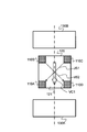
- the Hall element magnetic sensing unit 1 When considering the Hall element as shown in FIG. 6, when the width W, the length L, the electron mobility ⁇ , the applied voltage Vdd of the power source 2 for flowing current, and the applied magnetic field are B, the Hall element magnetic sensing unit 1
- an output voltage is generated even when no magnetic field is applied.
- the voltage output when the magnetic field is 0 is referred to as an offset voltage.
- the cause of the offset voltage is considered to be due to an imbalance in potential distribution inside the device such as mechanical stress applied to the device from the outside or misalignment during the manufacturing process.
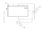
- FIG. 7 is a circuit diagram showing the principle of an offset cancel circuit using spinning current.
- the Hall element 10 has a symmetric shape, and has four terminals T1, T2, T3, and T4 for supplying a control current to a pair of input terminals and obtaining an output voltage from the other pair of output terminals. .
- the other pair of terminals T3 and T4 is a Hall voltage output terminal.
- Vh represents a Hall voltage proportional to the magnetic field generated by the Hall element
- Vos represents an offset voltage.
- the offset voltage Vos is canceled by subtracting the output voltage when a current is passed in the above two directions, and an output voltage 2Vh proportional to the magnetic field can be obtained (see, for example, Patent Document 1).
- the offset cancel circuit may not be able to completely cancel the offset voltage, which will be described below.
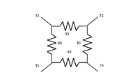
- the Hall element is represented by an equivalent circuit shown in FIG. That is, the Hall element can be expressed as a bridge circuit in which four terminals are connected by four resistors R1, R2, R3, and R4. As described above, canceling the offset voltage by subtracting the output voltage when a current is passed in two directions will be described with reference to this model.
- Vouta (R2 * R4-R1 * R3) / (R1 + R4) / (R2 + R3) * Vin Is output.
- Voutb (R1 * R3-R2 * R4) / (R3 + R4) / (R1 + R2) * Vin Is output.
- the structure of the Hall element is generally surrounded by a P-type impurity region for isolation at the periphery of an N-type impurity region that becomes a Hall element magnetic sensing portion.
- a depletion layer spreads at the boundary between the Hall element magnetic sensing part and its peripheral part. Since no hole current flows in the depletion layer, the hole current is suppressed and the resistance increases in the region where the depletion layer extends.
- the depletion layer width depends on the applied voltage. Therefore, since the values of the resistors R1, R2, R3, and R4 of the equivalent circuit shown in FIG. 8 change depending on the voltage application direction, the magnetic offset cancellation may not be performed by the offset cancel circuit.
- a depletion layer control electrode is arranged around the element and at the top of the element, and the depletion layer is controlled by adjusting the voltage applied to each electrode so that the depletion layer extends into the Hall element (for example, , See Patent Document 2).
- the resistance in the Hall element 10 is also not uniform in temperature, so the resistance value is not uniform and the resistance value is low and the resistance value is high. There will be a place. If an offset cancellation is performed by spinning current, the resistance values of the resistors R1, R2, R3, and R4 change depending on the temperature, and the offset cannot be canceled.
- the resistance value can be adjusted by the method of Patent Document 2, since a complicated control circuit is required using a plurality of depletion layer control electrodes, the chip size is increased, leading to an increase in cost. There is a difficulty such as.
- a temperature distribution is generated in the hall element 120 due to the influence of heat generation without increasing the chip area such as a complicated correction circuit or a distance. It is an object of the present invention to provide a hall sensor capable of canceling an offset by a spinning current even if the occurrence of the problem occurs.
- the present invention is configured as follows.
- a Hall element provided on a semiconductor substrate;
- An element serving as a heat source provided around the Hall element;
- Two pairs of terminals serving as a control current input terminal and a Hall voltage output terminal, which are disposed in the Hall element, In the two pairs of terminals, the Hall element control current 1 flowing between the pair of terminals and the Hall element control current 2 flowing between the other pair of terminals intersect as a vector,
- the Hall element has a line-symmetric shape with respect to a straight line along a vector sum of the Hall element control current 1 and the Hall element control current 2;
- the element serving as the heat source is a Hall sensor characterized in that the center of the heat source is located on a straight line along the vector sum of the Hall element control current 1 and the Hall element control current 2.
- FIG. 1 is a plan view of a Hall sensor representing a first embodiment according to the present invention.
- the Hall sensor includes a Hall element that senses magnetism and a circuit that drives or controls the Hall element.
- the Hall element 120 is composed of a magnetic sensing part made up of a square N-type impurity region 121 and an N-type high-concentration impurity region of the same shape arranged at each vertex of the square magnetic sensing part on a semiconductor substrate.
- a control current input terminal and a Hall voltage output terminal 110A, 110B, 110C, 110D are provided.
- a circuit for driving the Hall element 120 is provided on the substrate on which the Hall element 120 is formed.
- the circuit includes an element that becomes the heat source 130.
- a voltage regulator or a resistance element through which a large current flows can be a heat source. Therefore, as shown in FIG. 1, the center of the heat source 130 is aligned with the Hall element 120 on a straight line along the vector sum VC1 of the Hall element control currents JS1 and JS2 in two directions by the spinning current method. As a result, it is possible to eliminate the influence of the heat from the heating element 130 on the offset of the Hall element.
- the center of the heat source means a point or region having the highest temperature corresponding to the top of the isotherm when an isotherm representing a temperature gradient is drawn when the heat source is viewed from above.
- the Hall element preferably has a shape that is line symmetric with respect to a straight line along the vector sum of the Hall element control currents JS1 and JS2 in two directions by the spinning current method.
- Vouta-Voutb (R1-R3) * (R2-R4) * (R2 * R4-R1 * R3) / (R1 + R4) / (R2 + R3) / (R3 + R4) / (R1 + R2) * Vin
- R2 becomes R2 '
- R4 becomes R4'.
- the difference in output voltage is a value represented by the following expression, and cannot be set to zero.
- Vouta′-Voutb ′ (R1′-R3 ′) * (R2′-R4 ′) * (R2 ′ * R4′-R1 ′ * R3 ′) / (R1 ′ + R4 ′) / (R2 ′ + R3 ′ ) / (R3 ′ + R4 ′) / (R1 ′ + R2 ′) * Vin
- the positional relationship between the Hall element and the heat source is adjusted to the resistance R2 by aligning the center of the heat source 130 with the extended line of the vector sum VC1 of the Hall element control currents JS1 and JS2 in two directions by the spinning current method as shown in FIG.
- FIG. 5 is an experimental diagram showing the maximum and minimum temperature difference in the Hall element and the magnetic field converted value of the offset after the offset removal by the spinning current.
- Legend A is a measurement result when the arrangement of Example 1 shown in FIG. 1 is taken
- Legend B is a measurement result when a heat source is arranged in a direction perpendicular to the Hall element control current vector sum VC1. From the measurement result of FIG. 5, it is understood that the offset can be removed by making the positional relationship between the Hall element and the heat source as shown in FIG.
- FIG. 2 is a plan view of the Hall sensor showing an embodiment of the present invention in the case where there are a plurality of elements (heat generation sources) 130A and 130B that generate heat in the circuit that controls the Hall element 120.
- the center of the heat source means a point or region having the highest temperature corresponding to the top of the isotherm when an isotherm representing a temperature gradient is drawn when the heat source is viewed from above.
- the Hall element preferably has a shape that is line symmetric along a straight line passing through the vector sum of the Hall element control currents JS1 and JS2 in two directions by the spinning current method.
- the center of the heat source 130 is on the extension line of the vector sum VC1 of the Hall element control currents JS1 and JS2.
- the shape of the Hall element 120 is not limited to a square as shown in FIG. As shown in FIG. 4, a magnetic sensing portion made of a cross-shaped N-type impurity region 121, and a hole current control electrode and a hall voltage output terminal (110A to 110D) made of an N-type high-concentration impurity region at its four ends. Also in the Hall element 120, the influence of the heat from the heating source 130 on the offset of the Hall element can be eliminated by aligning the center of the heating source 130 with the extension line of the vector sum VC1 of the Hall element control currents JS1 and JS2. And offset removal is possible.
- the shape of the Hall element is a shape having line symmetry such as a square or a cross shape
- the center of the heat generating source 130 is aligned with the extension line of the vector sum VC1 of the Hall element control currents JS1 and JS2, thereby causing the spinning current to Offset removal is possible.
- the center of the heat source means a point or region having the highest temperature corresponding to the top of the isotherm when an isotherm representing a temperature gradient is drawn when the heat source is viewed from above.
- the Hall element preferably has a shape that is line symmetric along a straight line passing through the vector sum of currents JS1 and JS2 in two directions by the spinning current method.
- the offset is caused by the spinning current.
- a Hall sensor that can be removed and has a small chip area and reduced cost can be realized.
Abstract
Description
VH=μB(W/L)Vdd
とあらわすことができる。印加磁場Bに比例する係数が磁気感度となるので、このホール素子の磁気感度Khは、
Kh=μ(W/L)Vdd
と表される。
図7はスピニングカレントによるオフセットキャンセル回路の原理を示す回路図である。ホール素子10は対称的な形状で、1対の入力端子に制御電流を流し、他の1対の出力端子から出力電圧を得るために、4端子T1、T2、T3、T4を有している。ホール素子の一方の一対の端子T1、T2が制御電流入力端子となる場合、他方の一対の端子T3、T4がホール電圧出力端子となる。このとき、入力端子に電圧Vinを印加すると、出力端子には出力電圧Vh+Vosが発生する。ここでVhはホール素子が発生する磁場に比例したホール電圧、Vosはオフセット電圧を示している。次に、T3、T4を制御電流出力端子、T1、T2をホール電圧出力端子として、T3、T4間に入力電圧Vinを印加すると、出力端子には電圧-Vh+Vosが発生する。S1~S4はセンサー端子切替手段であり、切替信号発生器11によりN1あるいはN2の端子が選択される。
ホール素子は、図8に示す等価回路で表される。即ち、ホール素子は、4つの端子を、4つの抵抗R1、R2、R3、R4で接続したブリッジ回路として表わすことが可能である。前記のとおり2方向に電流を流したときの出力電圧を減算することによりオフセット電圧をキャンセルすることをこのモデルにより説明する。
Vouta = (R2*R4-R1*R3)/(R1+R4)/(R2+R3)*Vin
が出力される。一方、端子T3、T4に電圧Vinを印加すると、T1、T2にはホール電圧
Voutb = (R1*R3-R2*R4)/(R3+R4)/(R1+R2)*Vin
が出力される。
Vouta-Voutb = (R1-R3)*(R2-R4)*(R2*R4-R1*R3)/(R1+R4)/(R2+R3)/(R3+R4)/(R1+R2)*Vin
となる。したがって、オフセット電圧は各々の等価回路の抵抗R1、R2、R3、R4が異なる場合でもR1=R3あるいはR2=R4であればオフセットをキャンセルすることができる。この場合、電圧を印加する端子を変えても各抵抗値は変化しないことを前提としている。しかし、この前提を満たさない場合、例えば一方向においてR1=R3とした場合でも、他方向においてこの関係を満たすことができなくなった場合、前記の差分をゼロとすることができないため、オフセットをキャンセルすることができなくなる。電圧の印加方向によりオフセットキャンセルができなくなる原因のひとつについて、さらに具体的に説明する。
半導体基板上に設けられたホール素子と、
前記ホール素子の周囲に設けられた発熱源となる素子と、
前記ホール素子に配置された、制御電流入力端子及びホール電圧出力端子を兼ねる二対の端子と、を有し、
前記二対の端子においては、一対の端子間に流すホール素子制御電流1と、他の一対の端子間に流すホール素子制御電流2とがベクトルとして交わっており、
前記ホール素子は前記ホール素子制御電流1と前記ホール素子制御電流2とのベクトル和に沿った直線に関し線対称な形状を有し、
前記発熱源となる素子は前記ホール素子制御電流1と前記ホール素子制御電流2とのベクトル和に沿った直線上に発熱源の中心が位置していることを特徴とするホールセンサである。
まず、ホール素子の形状について説明する。図1に示すようにホール素子120は半導体基板上に正方形のN型不純物領域121からなる磁気感受部と正方形の磁気感受部の各頂点に配置された同一形状のN型高濃度不純物領域からなる制御電流入力端子及びホール電圧出力端子110A,110B,110C,110Dを有する。上記形態のホール素子120にすることにより、対称性をもつ、ホール素子となる。
ホール素子はスピニングカレント法による2方向のホール素子制御電流JS1及びJS2のベクトル和に沿った直線に関し線対称となる形状を有することが好ましい。
図1のホール素子120のN型高濃度不純物領域の制御電流端子及びホール電圧出力端子110A、110B、110C、110Dは、それぞれ図7のT1、T3、T2、T4に接続される。図8の等価回路を用いると、ここでは室温で温度勾配がない場合はR2=R4が成り立っているとする。このためスピニングカレントによりオフセットをキャンセルすることが可能であることになる。次に、各抵抗の温度が異なっていたり温度勾配があったりすると、各抵抗値は異なってしまう。即ち、R2はR2′となり、R4はR4′となるとする。温度勾配があれば一般にはR2′≠R4′となってしまう。なお、ここで、R1≠R3であり、温度勾配が生じてもR1′≠R3′である。
Vouta = (R2*R4-R1*R3)/(R1+R4)/(R2+R3)*Vin
が出力される。一方、端子T3、T4に電圧Vinを印加すると、電流JS2が流れ、T1、T2にはホール電圧
Voutb = (R1*R3-R2*R4)/(R3+R4)/(R1+R2)*Vin
が出力される。
Vouta-Voutb = (R1-R3)*(R2-R4)*(R2*R4-R1*R3)/(R1+R4)/(R2+R3)/(R3+R4)/(R1+R2)*Vin
しかし、温度勾配が生ずると、抵抗値は異なってしまい、R2はR2′となり、R4はR4′となる。そのため、出力電圧の差は以下の式で表される値となり、ゼロとすることはできなくなる。
Vouta′-Voutb′ = (R1′-R3′)*(R2′-R4′)*(R2′*R4′-R1′*R3′)/(R1′+R4′)/(R2′+R3′)/
(R3′+R4′)/(R1′+R2′)*Vin
しかし、ホール素子と発熱源の位置関係を図1のようにスピニングカレント法による2方向のホール素子制御電流JS1及びJS2のベクトル和VC1の延長線上に発熱源130の中心を合わせることにより、抵抗R2、R4は発熱の影響を受けてR2′、R4′となっても、2方向のホール素子制御電流JS1及びJS2のベクトル和VC1に沿った直線に対し、対称に配置されているので、同じ温度勾配のもとにあることとなり、R2=R4の関係を維持したまま、R2′=R4′となることが可能である。
したがって、出力電圧の差をとると
Vout=Vouta′-Voutb′=0
となり、スピニングカレントによるオフセット電圧が除去可能となる。
ホール素子はスピニングカレント法による2方向のホール素子制御電流JS1及びJS2のベクトル和を通る直線に沿って線対称となる形状を有することが好ましい。
ホール素子はスピニングカレント法による2方向の電流JS1及びJS2のベクトル和を通る直線に沿って線対称となる形状を有することが好ましい。
121 N型不純物領域
130、130A、130B ホール素子駆動回路発熱源
110A、110B、110C、110D N型高濃度不純物領域からなるホール電圧出力端子及び制御電流入力端子
2、12 電源
3、13 電圧計
11 切替信号発生器
S1、S2、S3、S4 センサー端子切替手段
T1、T2、T3、T4 端子
R1、R2、R3、R4 抵抗
JS1,JS2 ホール素子制御電流
VC1 ホール素子制御電流ベクトル和
Claims (3)
- 半導体基板上に設けられたホール素子と、
前記ホール素子の周囲に設けられた発熱源となる素子と、
前記ホール素子に配置された、制御電流入力端子及びホール電圧出力端子を兼ねる二対の端子と、を有し、
前記二対の端子においては、一対の端子間に流す第1のホール素子制御電流と、他の一対の端子間に流す第2のホール素子制御電流とがベクトルとして交わっており、
前記ホール素子は、前記第1のホール素子制御電流と前記第2のホール素子制御電流とのベクトル和に沿った直線に関し線対称な形状を有し、
前記発熱源となる素子は、前記第1のホール素子制御電流と前記第2のホール素子制御電流2とのベクトル和に沿った直線上に発熱源の中心が位置していることを特徴とするホールセンサ。 - 前記ホール素子は、正方形もしくは十字型の対称性を有する磁気感受部と、その各頂点及び端部に同一形状のN型高濃度不純物領域の制御電流入力端子及びホール電圧出力端子を有することを特徴とする請求項1記載のホールセンサ。
- スピニングカレントによりオフセット電圧を除去できることを特徴とする請求項1または2に記載のホールセンサ。
Priority Applications (4)
| Application Number | Priority Date | Filing Date | Title |
|---|---|---|---|
| CN201580052308.3A CN106716164A (zh) | 2014-09-30 | 2015-08-28 | 霍尔传感器 |
| KR1020177011478A KR20170061700A (ko) | 2014-09-30 | 2015-08-28 | 홀 센서 |
| EP15845690.5A EP3203253B1 (en) | 2014-09-30 | 2015-08-28 | Hall sensor |
| US15/469,789 US20170199252A1 (en) | 2014-09-30 | 2017-03-27 | Hall sensor |
Applications Claiming Priority (2)
| Application Number | Priority Date | Filing Date | Title |
|---|---|---|---|
| JP2014-202015 | 2014-09-30 | ||
| JP2014202015A JP2016070829A (ja) | 2014-09-30 | 2014-09-30 | ホールセンサ |
Related Child Applications (1)
| Application Number | Title | Priority Date | Filing Date |
|---|---|---|---|
| US15/469,789 Continuation US20170199252A1 (en) | 2014-09-30 | 2017-03-27 | Hall sensor |
Publications (1)
| Publication Number | Publication Date |
|---|---|
| WO2016052028A1 true WO2016052028A1 (ja) | 2016-04-07 |
Family
ID=55630074
Family Applications (1)
| Application Number | Title | Priority Date | Filing Date |
|---|---|---|---|
| PCT/JP2015/074318 WO2016052028A1 (ja) | 2014-09-30 | 2015-08-28 | ホールセンサ |
Country Status (7)
| Country | Link |
|---|---|
| US (1) | US20170199252A1 (ja) |
| EP (1) | EP3203253B1 (ja) |
| JP (1) | JP2016070829A (ja) |
| KR (1) | KR20170061700A (ja) |
| CN (1) | CN106716164A (ja) |
| TW (1) | TW201617636A (ja) |
| WO (1) | WO2016052028A1 (ja) |
Families Citing this family (3)
| Publication number | Priority date | Publication date | Assignee | Title |
|---|---|---|---|---|
| EP3401646B1 (en) * | 2017-05-09 | 2020-04-15 | Melexis Technologies SA | Bridge sensor error check |
| DE102018111753A1 (de) * | 2018-05-16 | 2019-11-21 | Infineon Technologies Ag | Konzept zur kompensation einer mechanischen verspannung einer in ein halbleitersubstrat integrierten hallsensorschaltung |
| JP7365771B2 (ja) * | 2019-01-31 | 2023-10-20 | エイブリック株式会社 | 半導体装置 |
Citations (2)
| Publication number | Priority date | Publication date | Assignee | Title |
|---|---|---|---|---|
| JP2013201229A (ja) * | 2012-03-23 | 2013-10-03 | Seiko Instruments Inc | ホールセンサ |
| JP2014066522A (ja) * | 2012-09-24 | 2014-04-17 | Seiko Instruments Inc | 半導体ホールセンサ |
Family Cites Families (8)
| Publication number | Priority date | Publication date | Assignee | Title |
|---|---|---|---|---|
| JPS63151090A (ja) * | 1986-12-16 | 1988-06-23 | Matsushita Electronics Corp | ホ−ル効果半導体装置 |
| JPH01291181A (ja) * | 1988-05-18 | 1989-11-22 | Mitsubishi Electric Corp | ホール素子の同相電圧除去回路 |
| JP4480318B2 (ja) * | 2002-02-13 | 2010-06-16 | 旭化成エレクトロニクス株式会社 | 複合半導体素子及びその製造方法 |
| NL1025089C2 (nl) * | 2003-12-19 | 2005-06-21 | Xensor Integration B V | Magneetveldsensor, drager van een dergelijke magneetveldsensor en een kompas, voorzien van een dergelijke magneetveldsensor. |
| DE102007044471A1 (de) * | 2007-09-18 | 2009-04-02 | Fraunhofer-Gesellschaft zur Förderung der angewandten Forschung e.V. | Verfahren zur abschnittsweisen Bestimmung eines parameterabhängigen Korrekturwertnäherungsverlaufs und Sensoranordnung |
| JP5815986B2 (ja) * | 2010-07-05 | 2015-11-17 | セイコーインスツル株式会社 | ホールセンサ |
| JP5679906B2 (ja) * | 2010-07-05 | 2015-03-04 | セイコーインスツル株式会社 | ホールセンサ |
| US9170307B2 (en) * | 2012-09-26 | 2015-10-27 | Infineon Technologies Ag | Hall sensors and sensing methods |
-
2014
- 2014-09-30 JP JP2014202015A patent/JP2016070829A/ja active Pending
-
2015
- 2015-08-28 CN CN201580052308.3A patent/CN106716164A/zh active Pending
- 2015-08-28 KR KR1020177011478A patent/KR20170061700A/ko unknown
- 2015-08-28 WO PCT/JP2015/074318 patent/WO2016052028A1/ja active Application Filing
- 2015-08-28 EP EP15845690.5A patent/EP3203253B1/en active Active
- 2015-09-03 TW TW104129217A patent/TW201617636A/zh unknown
-
2017
- 2017-03-27 US US15/469,789 patent/US20170199252A1/en not_active Abandoned
Patent Citations (2)
| Publication number | Priority date | Publication date | Assignee | Title |
|---|---|---|---|---|
| JP2013201229A (ja) * | 2012-03-23 | 2013-10-03 | Seiko Instruments Inc | ホールセンサ |
| JP2014066522A (ja) * | 2012-09-24 | 2014-04-17 | Seiko Instruments Inc | 半導体ホールセンサ |
Non-Patent Citations (1)
| Title |
|---|
| See also references of EP3203253A4 * |
Also Published As
| Publication number | Publication date |
|---|---|
| US20170199252A1 (en) | 2017-07-13 |
| JP2016070829A (ja) | 2016-05-09 |
| EP3203253A4 (en) | 2018-06-20 |
| EP3203253A1 (en) | 2017-08-09 |
| KR20170061700A (ko) | 2017-06-05 |
| TW201617636A (zh) | 2016-05-16 |
| CN106716164A (zh) | 2017-05-24 |
| EP3203253B1 (en) | 2019-07-31 |
Similar Documents
| Publication | Publication Date | Title |
|---|---|---|
| JP6483418B2 (ja) | ホールセンサおよびホールセンサの温度によるオフセットの補償方法 | |
| JP5679906B2 (ja) | ホールセンサ | |
| JP5815986B2 (ja) | ホールセンサ | |
| JP6489840B2 (ja) | ホール素子 | |
| WO2016052028A1 (ja) | ホールセンサ | |
| WO2013140984A1 (ja) | ホールセンサ | |
| WO2013140985A1 (ja) | ホールセンサ | |
| JP6043076B2 (ja) | ホールセンサ | |
| KR101820756B1 (ko) | 저항오차 보정기능을 갖는 홀 플레이트 | |
| JPS5950119B2 (ja) | ホ−ル効果装置 |
Legal Events
| Date | Code | Title | Description |
|---|---|---|---|
| 121 | Ep: the epo has been informed by wipo that ep was designated in this application |
Ref document number: 15845690 Country of ref document: EP Kind code of ref document: A1 |
|
| NENP | Non-entry into the national phase |
Ref country code: DE |
|
| REEP | Request for entry into the european phase |
Ref document number: 2015845690 Country of ref document: EP |
|
| WWE | Wipo information: entry into national phase |
Ref document number: 2015845690 Country of ref document: EP |
|
| ENP | Entry into the national phase |
Ref document number: 20177011478 Country of ref document: KR Kind code of ref document: A |