WO2016050025A1 - 3d面板及其制备方法和具有所述3d面板的3d显示装置 - Google Patents
3d面板及其制备方法和具有所述3d面板的3d显示装置 Download PDFInfo
- Publication number
- WO2016050025A1 WO2016050025A1 PCT/CN2015/071968 CN2015071968W WO2016050025A1 WO 2016050025 A1 WO2016050025 A1 WO 2016050025A1 CN 2015071968 W CN2015071968 W CN 2015071968W WO 2016050025 A1 WO2016050025 A1 WO 2016050025A1
- Authority
- WO
- WIPO (PCT)
- Prior art keywords
- substrate
- signal
- signal electrode
- panel
- common electrode
- Prior art date
- Legal status (The legal status is an assumption and is not a legal conclusion. Google has not performed a legal analysis and makes no representation as to the accuracy of the status listed.)
- Ceased
Links
Images




Classifications
-
- G—PHYSICS
- G02—OPTICS
- G02F—OPTICAL DEVICES OR ARRANGEMENTS FOR THE CONTROL OF LIGHT BY MODIFICATION OF THE OPTICAL PROPERTIES OF THE MEDIA OF THE ELEMENTS INVOLVED THEREIN; NON-LINEAR OPTICS; FREQUENCY-CHANGING OF LIGHT; OPTICAL LOGIC ELEMENTS; OPTICAL ANALOGUE/DIGITAL CONVERTERS
- G02F1/00—Devices or arrangements for the control of the intensity, colour, phase, polarisation or direction of light arriving from an independent light source, e.g. switching, gating or modulating; Non-linear optics
- G02F1/01—Devices or arrangements for the control of the intensity, colour, phase, polarisation or direction of light arriving from an independent light source, e.g. switching, gating or modulating; Non-linear optics for the control of the intensity, phase, polarisation or colour
- G02F1/13—Devices or arrangements for the control of the intensity, colour, phase, polarisation or direction of light arriving from an independent light source, e.g. switching, gating or modulating; Non-linear optics for the control of the intensity, phase, polarisation or colour based on liquid crystals, e.g. single liquid crystal display cells
- G02F1/133—Constructional arrangements; Operation of liquid crystal cells; Circuit arrangements
- G02F1/1333—Constructional arrangements; Manufacturing methods
- G02F1/1343—Electrodes
- G02F1/134309—Electrodes characterised by their geometrical arrangement
-
- G—PHYSICS
- G02—OPTICS
- G02B—OPTICAL ELEMENTS, SYSTEMS OR APPARATUS
- G02B30/00—Optical systems or apparatus for producing three-dimensional [3D] effects, e.g. stereoscopic images
-
- G—PHYSICS
- G02—OPTICS
- G02B—OPTICAL ELEMENTS, SYSTEMS OR APPARATUS
- G02B30/00—Optical systems or apparatus for producing three-dimensional [3D] effects, e.g. stereoscopic images
- G02B30/20—Optical systems or apparatus for producing three-dimensional [3D] effects, e.g. stereoscopic images by providing first and second parallax images to an observer's left and right eyes
- G02B30/26—Optical systems or apparatus for producing three-dimensional [3D] effects, e.g. stereoscopic images by providing first and second parallax images to an observer's left and right eyes of the autostereoscopic type
- G02B30/27—Optical systems or apparatus for producing three-dimensional [3D] effects, e.g. stereoscopic images by providing first and second parallax images to an observer's left and right eyes of the autostereoscopic type involving lenticular arrays
-
- G—PHYSICS
- G02—OPTICS
- G02B—OPTICAL ELEMENTS, SYSTEMS OR APPARATUS
- G02B30/00—Optical systems or apparatus for producing three-dimensional [3D] effects, e.g. stereoscopic images
- G02B30/20—Optical systems or apparatus for producing three-dimensional [3D] effects, e.g. stereoscopic images by providing first and second parallax images to an observer's left and right eyes
- G02B30/26—Optical systems or apparatus for producing three-dimensional [3D] effects, e.g. stereoscopic images by providing first and second parallax images to an observer's left and right eyes of the autostereoscopic type
- G02B30/30—Optical systems or apparatus for producing three-dimensional [3D] effects, e.g. stereoscopic images by providing first and second parallax images to an observer's left and right eyes of the autostereoscopic type involving parallax barriers
- G02B30/31—Optical systems or apparatus for producing three-dimensional [3D] effects, e.g. stereoscopic images by providing first and second parallax images to an observer's left and right eyes of the autostereoscopic type involving parallax barriers involving active parallax barriers
-
- G—PHYSICS
- G02—OPTICS
- G02F—OPTICAL DEVICES OR ARRANGEMENTS FOR THE CONTROL OF LIGHT BY MODIFICATION OF THE OPTICAL PROPERTIES OF THE MEDIA OF THE ELEMENTS INVOLVED THEREIN; NON-LINEAR OPTICS; FREQUENCY-CHANGING OF LIGHT; OPTICAL LOGIC ELEMENTS; OPTICAL ANALOGUE/DIGITAL CONVERTERS
- G02F1/00—Devices or arrangements for the control of the intensity, colour, phase, polarisation or direction of light arriving from an independent light source, e.g. switching, gating or modulating; Non-linear optics
- G02F1/01—Devices or arrangements for the control of the intensity, colour, phase, polarisation or direction of light arriving from an independent light source, e.g. switching, gating or modulating; Non-linear optics for the control of the intensity, phase, polarisation or colour
- G02F1/13—Devices or arrangements for the control of the intensity, colour, phase, polarisation or direction of light arriving from an independent light source, e.g. switching, gating or modulating; Non-linear optics for the control of the intensity, phase, polarisation or colour based on liquid crystals, e.g. single liquid crystal display cells
- G02F1/133—Constructional arrangements; Operation of liquid crystal cells; Circuit arrangements
- G02F1/1333—Constructional arrangements; Manufacturing methods
- G02F1/133345—Insulating layers
-
- G—PHYSICS
- G02—OPTICS
- G02F—OPTICAL DEVICES OR ARRANGEMENTS FOR THE CONTROL OF LIGHT BY MODIFICATION OF THE OPTICAL PROPERTIES OF THE MEDIA OF THE ELEMENTS INVOLVED THEREIN; NON-LINEAR OPTICS; FREQUENCY-CHANGING OF LIGHT; OPTICAL LOGIC ELEMENTS; OPTICAL ANALOGUE/DIGITAL CONVERTERS
- G02F1/00—Devices or arrangements for the control of the intensity, colour, phase, polarisation or direction of light arriving from an independent light source, e.g. switching, gating or modulating; Non-linear optics
- G02F1/01—Devices or arrangements for the control of the intensity, colour, phase, polarisation or direction of light arriving from an independent light source, e.g. switching, gating or modulating; Non-linear optics for the control of the intensity, phase, polarisation or colour
- G02F1/13—Devices or arrangements for the control of the intensity, colour, phase, polarisation or direction of light arriving from an independent light source, e.g. switching, gating or modulating; Non-linear optics for the control of the intensity, phase, polarisation or colour based on liquid crystals, e.g. single liquid crystal display cells
- G02F1/133—Constructional arrangements; Operation of liquid crystal cells; Circuit arrangements
- G02F1/1333—Constructional arrangements; Manufacturing methods
- G02F1/1341—Filling or closing of cells
-
- G—PHYSICS
- G02—OPTICS
- G02F—OPTICAL DEVICES OR ARRANGEMENTS FOR THE CONTROL OF LIGHT BY MODIFICATION OF THE OPTICAL PROPERTIES OF THE MEDIA OF THE ELEMENTS INVOLVED THEREIN; NON-LINEAR OPTICS; FREQUENCY-CHANGING OF LIGHT; OPTICAL LOGIC ELEMENTS; OPTICAL ANALOGUE/DIGITAL CONVERTERS
- G02F1/00—Devices or arrangements for the control of the intensity, colour, phase, polarisation or direction of light arriving from an independent light source, e.g. switching, gating or modulating; Non-linear optics
- G02F1/01—Devices or arrangements for the control of the intensity, colour, phase, polarisation or direction of light arriving from an independent light source, e.g. switching, gating or modulating; Non-linear optics for the control of the intensity, phase, polarisation or colour
- G02F1/13—Devices or arrangements for the control of the intensity, colour, phase, polarisation or direction of light arriving from an independent light source, e.g. switching, gating or modulating; Non-linear optics for the control of the intensity, phase, polarisation or colour based on liquid crystals, e.g. single liquid crystal display cells
- G02F1/133—Constructional arrangements; Operation of liquid crystal cells; Circuit arrangements
- G02F1/1333—Constructional arrangements; Manufacturing methods
- G02F1/1343—Electrodes
- G02F1/13439—Electrodes characterised by their electrical, optical, physical properties; materials therefor; method of making
-
- G—PHYSICS
- G02—OPTICS
- G02F—OPTICAL DEVICES OR ARRANGEMENTS FOR THE CONTROL OF LIGHT BY MODIFICATION OF THE OPTICAL PROPERTIES OF THE MEDIA OF THE ELEMENTS INVOLVED THEREIN; NON-LINEAR OPTICS; FREQUENCY-CHANGING OF LIGHT; OPTICAL LOGIC ELEMENTS; OPTICAL ANALOGUE/DIGITAL CONVERTERS
- G02F1/00—Devices or arrangements for the control of the intensity, colour, phase, polarisation or direction of light arriving from an independent light source, e.g. switching, gating or modulating; Non-linear optics
- G02F1/01—Devices or arrangements for the control of the intensity, colour, phase, polarisation or direction of light arriving from an independent light source, e.g. switching, gating or modulating; Non-linear optics for the control of the intensity, phase, polarisation or colour
- G02F1/13—Devices or arrangements for the control of the intensity, colour, phase, polarisation or direction of light arriving from an independent light source, e.g. switching, gating or modulating; Non-linear optics for the control of the intensity, phase, polarisation or colour based on liquid crystals, e.g. single liquid crystal display cells
- G02F1/133—Constructional arrangements; Operation of liquid crystal cells; Circuit arrangements
- G02F1/1333—Constructional arrangements; Manufacturing methods
- G02F1/1345—Conductors connecting electrodes to cell terminals
Definitions
- the present invention relates to the field of 3D display technologies, and in particular, to an active grating 3D panel, a method for fabricating the same, and a 3D display device having the same.
- Stereoscopic display ie, three-dimensional (3D) display
- 3D three-dimensional
- the basic principle of stereoscopic display is that the parallax produces a stereoscopic effect, that is, the left eye of the person sees the left eye image, and the right eye sees the right eye image, wherein the left and right eye images are a pair of stereoscopic image pairs with parallax.
- One way to achieve stereoscopic display is to use serial type, that is, at the first moment, the display displays the left eye picture, at this time only the left eye of the viewer sees the display picture; at the second time, the display shows the right eye picture, only let The viewer's right eye sees the display screen, and the persistence of the image in the retina of the human eye makes it possible for the left and right eyes to see the left and right eye images at the same time, thereby generating a three-dimensional feeling.
- Another way to realize stereoscopic display is parallel, that is, at the same time, a part of the pixels on the display display the content of the left eye picture, and some pixels display the content of the right eye picture, and the display of a part of the pixels is only performed by means of a grating or polarized glasses. It can be seen by the right eye, and the other part can only be seen by the left eye, resulting in a three-dimensional feeling.
- the display mode is gradually unable to meet the demand for 3D display.
- the naked-eye 3D display mode for example, a raster-type naked-eye 3D display device, since the grating is directly disposed in the display panel without wearing a 3D eye, it is more convenient to watch, and thus has received more and more attention.
- the present invention proposes a 3D panel for the above-described naked-eye 3D display.
- the present invention provides a The 3D panel and the preparation method thereof and the 3D display device including the 3D panel, wherein the two sides of the 3D display panel are fully utilized, and gratings having two periods are respectively fabricated on the upper and lower substrates of the 3D panel, and the signals are switched.
- the physical view point of the same panel 3D display can be switched, and the same 3D panel can be compatible with two different resolutions, that is, the two 3D displays share the purpose of sharing one 3D panel, and finally realize the economic benefit of reducing development cost.
- a 3D panel includes a first substrate, a second substrate, and a liquid crystal filled between the first substrate and the second substrate, wherein the first substrate and the first A common electrode and a signal electrode are disposed on the two substrates.
- the first substrate includes, in order from top to bottom, a first substrate, a first common electrode, a first common electrode lead, a first insulating layer, a first signal electrode lead, and a second insulating layer.
- the first signal electrode; the second substrate comprises, in order from bottom to top, a second substrate, a second common electrode, a second common electrode lead, a third insulating layer, a second signal electrode lead, a fourth insulating layer, and a second signal electrode; the first signal electrode is opposite to the second signal electrode.
- the first signal electrode and the second signal electrode are a plurality of sets of strip electrodes, and the strip electrodes of the first signal electrode and the strip electrodes of the second signal electrode are arranged in a wrong direction.
- the plurality of sets of strip electrodes as the first signal electrodes are evenly arranged and have a first period
- the plurality of sets of strip electrodes as the second signal electrodes are evenly arranged and have a second period The first period is different from the second period.
- the spacing between the plurality of sets of strip electrodes of the first signal electrode is greater than or equal to 10 microns, and the spacing between the plurality of sets of strip electrodes of the second signal electrode is greater than or equal to 10 microns.
- the first common electrode lead and the first signal electrode lead are each in a frame shape, and a signal access portion is disposed on one side of the first substrate; the second common electrode lead The second signal electrode leads are all frame-shaped, and a signal access portion is disposed on one side of the second substrate.
- the first common electrode, the first signal electrode, the second common electrode, and the second signal electrode are each made of a transparent conductive material.
- the first common electrode and the second common electrode are planar electrodes.
- the 3D panel further includes: a signal control module, configured to enable a signal electrode lead of the corresponding substrate when the viewpoint of the first or second substrate is gated.
- a signal control module configured to enable a signal electrode lead of the corresponding substrate when the viewpoint of the first or second substrate is gated.
- a 3D display device that includes a 3D panel as described above.
- a method for fabricating a 3D panel comprising the following steps:
- the first signal electrode of the first substrate is opposite to the second signal electrode of the second substrate, and the first substrate and the second substrate are A liquid crystal is filled between them to form the 3D panel.
- the electrodes on the two sides of the 3D panel of the present invention can be independently controlled.
- the switching of the upper and lower substrate grating electrodes can be realized, thereby improving the application range of the 3D panel and enhancing the compatibility of the 3D panel. Sex and versatility.
- FIG. 1 is a cross-sectional structural view of a 3D panel according to an embodiment of the invention.
- FIG. 2 is a cross-sectional structural view of a 3D display panel according to an embodiment of the invention.
- 3A-3F' are flowcharts showing a process of preparing a 3D panel according to an embodiment of the present invention.
- FIG. 4 is a cross-sectional view of a 3D display panel made in accordance with an embodiment of the present invention.
- a 3D panel for, for example, a naked-eye 3D display.
- the 3D panel includes a first substrate, a second substrate, and a first substrate and the first substrate. a liquid crystal between two substrates, wherein:
- a common electrode and a signal electrode are disposed on the first substrate and the second substrate.
- the first substrate includes, in order from top to bottom, a first substrate 1, a first common electrode 2, a first common electrode lead 3, a first insulating layer 4, and a first signal electrode. a lead 5, a second insulating layer 6, and a first signal electrode 7, wherein:
- the material of the first base substrate 1 may be a material such as glass, silicon wafer, quartz, plastic, or silicon wafer.
- the first common electrode 2 and the first signal electrode 7 are both made of a transparent conductive material, which may be a transparent metal film, a transparent metal oxide film, a non-metal oxide film, and a conductive particle-dispersed ferroelectric
- a transparent conductive material which may be a transparent metal film, a transparent metal oxide film, a non-metal oxide film, and a conductive particle-dispersed ferroelectric
- the film may be in the form of a single layer film, a two layer film, a multilayer film or a multilayer film, an undoped type, a doped type, and a multi-element type.
- the transparent conductive material is a metal oxide film such as an indium tin oxide (ITO) film.
- the first common electrode lead 3 and the first signal electrode lead 5 are each made of a conductive material, and preferably, the conductive material is a metal material.
- the first insulating layer 4 is for isolating the first common electrode lead 3 and the first signal electrode lead 5.
- the first signal electrode 7 is electrically connected to the first signal electrode lead 5 through the via.
- the first insulating layer 4 and the second insulating layer 6 are both made of a transparent insulating material.
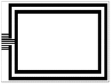
- the first common electrode lead 3 and the first signal electrode lead 5 are frame-shaped, and a signal access portion is disposed on one side of the first base substrate 1. It should be understood by those skilled in the art that the position of the signal access portion of the first common electrode lead 3 and the first signal electrode lead 5 is similar (as shown in FIG. 3D) for the convenience of signal access, which is for the present invention. It does not constitute a limitation.
- first common electrode lead 3 is located at the periphery of the first base substrate 1 (as shown in FIG. 3B). Shown), the first signal electrode lead 5 is located inside the first common electrode lead 3 (as shown in FIG. 3D).
- first common electrode lead 3 and the first signal electrode lead 5 may have other shapes as long as they can be electrically connected to the first common electrode 2 and the first signal electrode 7, respectively.
- the first common electrode 2 is a planar electrode
- the first signal electrode 7 is a plurality of sets of strip electrodes.
- the first signal electrode 7 is a plurality of sets of strip electrodes, and each set of strip electrodes is electrically connected to the first signal electrode lead 5 through corresponding via holes. Further, the plurality of sets of strip electrodes are placed obliquely. In a preferred embodiment, the plurality of sets of strip electrodes of the first signal electrode 7 are evenly arranged and have a first period.
- the second substrate includes, in order from bottom to top, a second substrate 1 ′, a second common electrode 2 ′, a second common electrode lead 3 ′, a third insulating layer 4 ′, Two signal electrode leads 5', a fourth insulating layer 6' and a second signal electrode 7', wherein:
- the second base substrate 1' may be made of a material such as glass, silicon wafer, quartz, plastic, or silicon wafer.
- the second common electrode 2' and the second signal electrode 7' are each made of a transparent conductive material, which may be a transparent metal film, a transparent metal oxide film, a non-metal oxide film, and conductive particle dispersion.
- the film may be in the form of a single layer film, a two layer film, a multilayer film or a multilayer film, an undoped type, a doped type, and a multi-element type.
- the transparent conductive material is a metal oxide film such as an indium tin oxide (ITO) film.
- the second common electrode lead 3' and the second signal electrode lead 5' are each made of a conductive material, and preferably, the conductive material is a metal material.
- the third insulating layer 4' is for isolating the second common electrode lead 3' and the second signal electrode lead 5'.
- the second signal electrode 7' is electrically connected to the second signal electrode lead 5' through the via.
- the third insulating layer 4' and the fourth insulating layer 6' are both made of a transparent insulating material.
- the second common electrode lead 3' and the second signal electrode lead 5' are each in a frame shape, and a signal access portion is disposed on one side of the second base substrate 1'.
- a signal access portion is disposed on one side of the second base substrate 1'.
- the second common electrode lead 3' is located at the periphery of the second base substrate 1' (as shown in FIG. 3B'), and the second signal electrode lead 5' is located at the second common electrode lead The inside of 3 (as shown in Figure 3D').
- the second common electrode lead 3' and the second signal electrode lead 5' may have other shapes as long as they can be electrically connected to the second common electrode 2' and the second signal electrode 7', respectively. .
- the second common electrode 2' is a planar electrode
- the second signal electrode 7' is a plurality of sets of strip electrodes.
- the second signal electrode 7' is a plurality of sets of strip electrodes, and each set of strip electrodes is electrically connected to the second signal electrode lead 5' through a corresponding via. Further, the plurality of sets of strip electrodes are placed obliquely. In a preferred embodiment, the plurality of sets of strip electrodes of the second signal electrode 7' are evenly arranged and have a second period, the second period being different from the first period.
- the first signal electrode 7 is opposite to the second signal electrode 7'.
- the strip electrodes of the first signal electrode 7 and the strip electrodes of the second signal electrode 7' are arranged in a wrong direction.
- the strip electrodes of the first signal electrode 7 and the strip electrodes of the second signal electrode 7' are obliquely arranged and inclined in different directions, and the two are not parallel.
- the first substrate and the second substrate have the same structure, and after the first substrate and the second substrate having the same structure are attached together in a signal electrode manner, the 3D panel is a first substrate and a second substrate.
- the center line between the substrates is a symmetrical pattern of the axis.
- the first substrate and the second substrate have the same structure, when the first substrate and the second substrate are prepared, such as forming a common electrode lead and a signal electrode lead, and the like
- the same reticle can be used in the graphic design, and the above-mentioned common design of the reticle can achieve the effect of reducing the production cost of the 3D panel.
- the enabling time of the first signal electrode 7 and the second signal electrode 7' to access the signal is different, for example, the time error of the first signal electrode 7 and the second signal electrode 7' to access the signal,
- the switching of the number of viewpoints of the 3D panel on the physical level can be realized, and the same 3D panel can be used to implement the liquid crystal panel with two different resolutions.
- the two 3D displays share the purpose of a 3D panel, ultimately achieving the economic benefits of reduced development costs.
- the 3D panel further includes a signal control module, configured to enable signal electrode leads of the corresponding substrate when the viewpoint of the first or second substrate is gated, even if the signal electrode leads of the corresponding substrate Access signal.
- a signal control module configured to enable signal electrode leads of the corresponding substrate when the viewpoint of the first or second substrate is gated, even if the signal electrode leads of the corresponding substrate Access signal.
- the second common electrode lead 3' is suspended, the second signal electrode lead 5' is connected to the signal; the first common electrode lead 3 and the first The signal electrode leads 5 are all connected to the common electrode signal.
- the second substrate realizes the grating function.
- the electrodes on the two sides of the 3D panel of the present invention can be independently controlled, by switching the signals of the upper and lower substrates, the switching of the upper and lower substrate grating electrodes can be realized, thereby improving the application range of the 3D panel and enhancing the 3D panel. Compatibility and versatility.
- a 3D display panel comprising the 3D panel as described above, the isolating glass 8 and the LCD panel 9, as shown in FIG.
- a 3D display device comprising the 3D panel as described above.
- a method of fabricating a 3D panel is also provided, such as shown in Figures 3A-3F', which comprises the following steps:
- first common electrode layer on the first base substrate 1 as a first common electrode 2 (Vcom) of the pixel, wherein the first common electrode 2 is a planar electrode, as shown in FIG. 3A;
- the first base substrate 1 may be made of materials such as glass, silicon wafer, quartz, plastic, and silicon wafer.
- the first common electrode layer is made of a transparent conductive material, and thus is not shown in FIG. 3A, and the transparent conductive material may be a transparent metal film, a transparent metal oxide film, a non-metal oxide film, and conductivity.
- the material may be a single layer film, a two layer film, a multilayer film or a multi-layer film, an undoped type, a doped type, and a multi-element type.
- the transparent conductive material is a metal oxide film such as an indium tin oxide (ITO) film.
- the first conductive layer is made of a conductive material, and preferably, the conductive material is a metal material.
- the first conductive layer may be formed by a process such as deposition, and the first common electrode lead 3 is formed by a patterning process such as exposure, etching, or the like.
- the first common electrode lead 3 has a frame shape, and a signal access portion is provided on one side of the first base substrate 1.
- first common electrode lead 3 may also have other shapes as long as it can be associated with the first public The electrode 2 can be electrically connected.
- first insulating layer 4 Forming a first insulating layer 4 on the first common electrode lead 3 to isolate the first common electrode lead 3 and the first signal electrode lead 5, as shown in FIG. 3C, wherein the first insulating layer 4 Made of a transparent insulating material and thus not shown in Figure 3C;
- the first insulating layer 4 can be formed by a process such as deposition.
- the second conductive layer is made of a conductive material, and preferably, the conductive material is a metal material.
- the second conductive layer may be formed by a process such as deposition, and the first signal electrode lead 5 is formed by a patterning process such as exposure, etching, or the like.
- the first signal electrode lead 5 also has a frame structure, and a signal access portion is also disposed on the same side of the signal access portion of the first common electrode lead 3, which is known in the art. It should be understood that the position of the signal access portion of the first common electrode lead 3 and the first signal electrode lead 5 is similar for the convenience of signal access, which is not limited to the present invention.
- the first signal electrode lead 5 may have other shapes as long as it can be electrically connected to the first signal electrode.
- the second insulating layer 6 may be formed by a process such as deposition, and a via hole is formed by etching or the like.
- the first signal electrode layer 7 is made of a transparent conductive material
- the transparent conductive material may be a transparent metal film, a transparent metal oxide film, a non-metal oxide film, and a conductive particle-dispersed ferroelectric material.
- the film may be in the form of a single layer film, a two layer film, a multilayer film or a multilayer film, an undoped type, a doped type, and a multi-element type.
- the transparent conductive material is a metal oxide film such as an indium tin oxide (ITO) film.
- the first signal electrode 7 is a plurality of sets of strip electrodes, and each set of strip electrodes passes Corresponding vias are electrically connected to the first signal electrode lead, and further, the plurality of sets of strip electrodes are placed obliquely.
- the plurality of sets of strip electrodes of the first signal electrode 7 are evenly arranged and have a first period.
- the second substrate is obtained, as shown in FIG. 3A', FIG. 3B', FIG. 3C', FIG. 3D', FIG. 3E', and FIG. 3F', only when the second signal electrode 7' of the second substrate is fabricated.
- the arrangement direction of the plurality of sets of strip electrodes of the second signal electrode 7' is opposite to the arrangement direction of the plurality of sets of strip electrodes of the first signal electrode, for example, as shown in FIGS. 3F and 3F'.
- the direction of the tilt is different.
- the plurality of sets of strip electrodes of the second signal electrode 7' are evenly arranged and have a second period different from the first period.
- a spacing between the plurality of sets of strip electrodes of the first signal electrode is greater than or equal to 10 micrometers
- a spacing between the plurality of strip electrodes of the second signal electrode is greater than or equal to 10 micrometers.
- the first substrate and the edge of the second substrate are bonded together, and a liquid crystal is filled between the first substrate and the second substrate to form the 3D panel.
- the structure of the second substrate is the same as the structure of the first substrate, and after the first substrate and the second substrate having the same structure are attached to each other with the signal electrodes facing each other, the 3D panel is a center line between the substrate and the second substrate is symmetrical with respect to the axis.
- a second common is formed on the second substrate.
- the electrode lead 3' and the second signal electrode lead 5', and other identical graphic designs, can share the same reticle with the first substrate, and the above-mentioned common design of the reticle can achieve the effect of reducing the production cost of the 3D panel.
- the first substrate and the second substrate are bonded together using a material such as a TN mode liquid crystal, a spherical spacer, or a polarizer.
- a material such as a TN mode liquid crystal, a spherical spacer, or a polarizer.
- FIG. 4 A cross-sectional view of a 3D display panel according to an embodiment of the present invention is shown in FIG. 4.
- FIG. 4 common electrode leads and signal electrode leads of the first substrate and the second substrate are respectively connected by an anisotropic conductive adhesive.
- two black areas between the first substrate and the second substrate are frame sealants.
- the conventional design of the active grating 3D display panel has only one periodic grating, so it can only be compatible with one kind of viewpoint display of a liquid crystal panel, which is inconvenient for the user's use and the manufacturer's production.
- the common substrate and the signal electrode are formed on the upper and lower substrates, that is, the first substrate and the second substrate, but the enabling time of the signal electrodes on the first substrate and the second substrate is wrong. That is, the time of the signal electrode access signal on the first substrate and the second substrate is phase-shifted, so that the signal switching between the first substrate and the second substrate can realize the physical layer switching of the number of viewpoints of the 3D panel.
- the purpose of the panel is to achieve economic benefits that reduce development costs.
- the signal electrode leads of the corresponding substrate are enabled even if the signal electrode leads of the corresponding substrate are connected to the signal, specifically, when the first substrate
- the viewpoint is gated, that is, when the first substrate is used as a working electrode: the first common electrode lead is suspended, the first signal electrode lead is connected to the signal, and the second common electrode lead and the second signal electrode lead are both connected to the common
- the first substrate implements a grating function.
- the second common electrode lead is suspended, the second signal electrode lead is connected to the signal, and the first common electrode lead and the first signal electrode lead The common electrode signals are all connected.
- the second substrate realizes the grating function.
- the electrodes on the two sides of the 3D panel of the present invention can be independently controlled, by switching the signals of the upper and lower substrates, the switching of the upper and lower substrate grating electrodes can be realized, thereby improving the application range of the 3D panel and enhancing the 3D panel. Compatibility and versatility.
Landscapes
- Physics & Mathematics (AREA)
- Nonlinear Science (AREA)
- General Physics & Mathematics (AREA)
- Optics & Photonics (AREA)
- Mathematical Physics (AREA)
- Chemical & Material Sciences (AREA)
- Crystallography & Structural Chemistry (AREA)
- Geometry (AREA)
- Liquid Crystal (AREA)
- Devices For Indicating Variable Information By Combining Individual Elements (AREA)
Priority Applications (4)
| Application Number | Priority Date | Filing Date | Title |
|---|---|---|---|
| EP15749962.5A EP3203312B1 (en) | 2014-09-30 | 2015-01-30 | 3d panel and preparation method therefor, and 3d display device provided with 3d panel |
| JP2017536996A JP6464273B2 (ja) | 2014-09-30 | 2015-01-30 | 3dパネルおよびその製造方法、並びに前記3dパネルを備えた3d表示装置 |
| US14/770,008 US9946085B2 (en) | 2014-09-30 | 2015-01-30 | 3D panel, method for producing the same, and 3D display apparatus having the same |
| KR1020157023125A KR101773691B1 (ko) | 2014-09-30 | 2015-01-30 | 3d 패널 및 그 제조방법과 상기 3d 패널을 구비한 3d 디스플레이 장치 |
Applications Claiming Priority (2)
| Application Number | Priority Date | Filing Date | Title |
|---|---|---|---|
| CN201410520459.4 | 2014-09-30 | ||
| CN201410520459.4A CN104298019B (zh) | 2014-09-30 | 2014-09-30 | 一种3d面板及其制备方法、3d显示装置 |
Publications (1)
| Publication Number | Publication Date |
|---|---|
| WO2016050025A1 true WO2016050025A1 (zh) | 2016-04-07 |
Family
ID=52317810
Family Applications (1)
| Application Number | Title | Priority Date | Filing Date |
|---|---|---|---|
| PCT/CN2015/071968 Ceased WO2016050025A1 (zh) | 2014-09-30 | 2015-01-30 | 3d面板及其制备方法和具有所述3d面板的3d显示装置 |
Country Status (6)
| Country | Link |
|---|---|
| US (1) | US9946085B2 (enExample) |
| EP (1) | EP3203312B1 (enExample) |
| JP (1) | JP6464273B2 (enExample) |
| KR (1) | KR101773691B1 (enExample) |
| CN (1) | CN104298019B (enExample) |
| WO (1) | WO2016050025A1 (enExample) |
Families Citing this family (4)
| Publication number | Priority date | Publication date | Assignee | Title |
|---|---|---|---|---|
| CN104298019B (zh) | 2014-09-30 | 2017-10-03 | 京东方科技集团股份有限公司 | 一种3d面板及其制备方法、3d显示装置 |
| CN104777693B (zh) * | 2015-04-28 | 2017-05-03 | 深圳市华星光电技术有限公司 | 高穿透率psva型液晶显示面板及其制作方法 |
| CN107436500B (zh) | 2017-08-25 | 2020-04-24 | 京东方科技集团股份有限公司 | 光栅及制备方法、驱动方法、裸眼三维显示系统 |
| JP6928016B2 (ja) * | 2019-02-26 | 2021-09-01 | パナソニック液晶ディスプレイ株式会社 | 液晶表示装置及び液晶表示装置の製造方法 |
Citations (6)
| Publication number | Priority date | Publication date | Assignee | Title |
|---|---|---|---|---|
| JPH08313938A (ja) * | 1995-05-19 | 1996-11-29 | Hitachi Ltd | 液晶表示装置 |
| CN102819153A (zh) * | 2012-08-10 | 2012-12-12 | 京东方科技集团股份有限公司 | 一种彩膜基板、液晶面板及液晶显示装置 |
| US20130278847A1 (en) * | 2012-04-18 | 2013-10-24 | Samsung Display Co., Ltd. | Liquid crystal lens panel and display device having the same |
| CN103383510A (zh) * | 2013-07-09 | 2013-11-06 | 京东方科技集团股份有限公司 | 一种液晶面板和显示装置 |
| CN103984107A (zh) * | 2014-05-04 | 2014-08-13 | 京东方科技集团股份有限公司 | 视差挡板及其制备方法、显示面板和显示装置 |
| CN104298019A (zh) * | 2014-09-30 | 2015-01-21 | 京东方科技集团股份有限公司 | 一种3d面板及其制备方法、3d显示装置 |
Family Cites Families (13)
| Publication number | Priority date | Publication date | Assignee | Title |
|---|---|---|---|---|
| US7359105B2 (en) * | 2006-02-07 | 2008-04-15 | Sharp Kabushiki Kaisha | Spatial light modulator and a display device |
| JP5356952B2 (ja) * | 2009-08-31 | 2013-12-04 | レムセン イノベーション、リミティッド ライアビリティー カンパニー | 表示装置 |
| TWI407195B (zh) * | 2009-12-30 | 2013-09-01 | Unique Instr Co Ltd | A full-screen three-dimensional image display device |
| TWI391738B (zh) * | 2010-01-08 | 2013-04-01 | Unique Instr Co Ltd | A device for multifunctional liquid crystal parallax gratings |
| KR20120130397A (ko) | 2011-05-23 | 2012-12-03 | 삼성디스플레이 주식회사 | 렌즈 모듈 및 이를 갖는 표시 장치 |
| US9036013B2 (en) * | 2011-06-20 | 2015-05-19 | Electronics And Telecommunications Research Institute | Segmented dual layer parallax barrier-based 3D display device and method |
| US9036014B2 (en) * | 2011-06-20 | 2015-05-19 | Electronics And Telecommunications Research Institute | Dual layer parallax barrier-based 3D display device and method |
| JP6178050B2 (ja) * | 2011-07-15 | 2017-08-09 | 株式会社半導体エネルギー研究所 | 表示装置 |
| KR101896695B1 (ko) * | 2011-10-05 | 2018-09-10 | 한국전자통신연구원 | 입체 영상 패널, 입체 영상 패널을 포함하는 입체 영상 표시 장치 및 그 구동 방법 |
| KR101937865B1 (ko) | 2012-02-09 | 2019-01-15 | 삼성디스플레이 주식회사 | 액정 렌즈 패널 및 이를 구비하는 표시 장치 |
| KR101899135B1 (ko) * | 2012-04-03 | 2018-09-17 | 삼성디스플레이 주식회사 | 시분할 액정 배리어 및 이를 포함하는 입체 영상 표시 장치 |
| US20140022241A1 (en) * | 2012-07-18 | 2014-01-23 | Electronics And Telecommunications Research Institute | Display apparatus and method based on symmetrically spb |
| CN103885636B (zh) * | 2014-03-10 | 2016-11-16 | 京东方科技集团股份有限公司 | 一种触摸显示装置及其制作方法 |
-
2014
- 2014-09-30 CN CN201410520459.4A patent/CN104298019B/zh active Active
-
2015
- 2015-01-30 JP JP2017536996A patent/JP6464273B2/ja active Active
- 2015-01-30 KR KR1020157023125A patent/KR101773691B1/ko active Active
- 2015-01-30 US US14/770,008 patent/US9946085B2/en active Active
- 2015-01-30 EP EP15749962.5A patent/EP3203312B1/en active Active
- 2015-01-30 WO PCT/CN2015/071968 patent/WO2016050025A1/zh not_active Ceased
Patent Citations (6)
| Publication number | Priority date | Publication date | Assignee | Title |
|---|---|---|---|---|
| JPH08313938A (ja) * | 1995-05-19 | 1996-11-29 | Hitachi Ltd | 液晶表示装置 |
| US20130278847A1 (en) * | 2012-04-18 | 2013-10-24 | Samsung Display Co., Ltd. | Liquid crystal lens panel and display device having the same |
| CN102819153A (zh) * | 2012-08-10 | 2012-12-12 | 京东方科技集团股份有限公司 | 一种彩膜基板、液晶面板及液晶显示装置 |
| CN103383510A (zh) * | 2013-07-09 | 2013-11-06 | 京东方科技集团股份有限公司 | 一种液晶面板和显示装置 |
| CN103984107A (zh) * | 2014-05-04 | 2014-08-13 | 京东方科技集团股份有限公司 | 视差挡板及其制备方法、显示面板和显示装置 |
| CN104298019A (zh) * | 2014-09-30 | 2015-01-21 | 京东方科技集团股份有限公司 | 一种3d面板及其制备方法、3d显示装置 |
Non-Patent Citations (1)
| Title |
|---|
| See also references of EP3203312A4 * |
Also Published As
| Publication number | Publication date |
|---|---|
| EP3203312A4 (en) | 2018-06-13 |
| US20160252735A1 (en) | 2016-09-01 |
| EP3203312B1 (en) | 2019-12-11 |
| CN104298019B (zh) | 2017-10-03 |
| US9946085B2 (en) | 2018-04-17 |
| CN104298019A (zh) | 2015-01-21 |
| JP6464273B2 (ja) | 2019-02-06 |
| KR101773691B1 (ko) | 2017-08-31 |
| EP3203312A1 (en) | 2017-08-09 |
| KR20160053839A (ko) | 2016-05-13 |
| JP2017530428A (ja) | 2017-10-12 |
Similar Documents
| Publication | Publication Date | Title |
|---|---|---|
| US9110303B2 (en) | 3D display panel and method of manufacturing phase difference plate | |
| CN103698893B (zh) | 立体液晶显示装置 | |
| US9103989B2 (en) | Method of manufacturing phase difference plate and 3D display panel | |
| US20160313565A1 (en) | Liquid crystal lens, manufacturing method and display device | |
| CN103149767B (zh) | 一种液晶透镜及包含该液晶透镜的裸眼立体显示装置 | |
| CN207882478U (zh) | 光栅结构及显示装置 | |
| CN103412441B (zh) | 阵列基板、彩膜基板、显示装置及取向层的制作方法 | |
| CN102929048A (zh) | 能同时兼容2d与3d的液晶狭缝光栅 | |
| CN101371182A (zh) | 立体图像显示装置 | |
| TWI354143B (en) | Liquid crystal display apparatus | |
| CN102141703B (zh) | 一种具有相位延迟膜的偏光式3d液晶屏 | |
| JP2013195994A (ja) | 製造装置、製造方法、光学素子、表示装置、および電子機器 | |
| CN102364391B (zh) | 立体显示设备和方法 | |
| JP6464273B2 (ja) | 3dパネルおよびその製造方法、並びに前記3dパネルを備えた3d表示装置 | |
| WO2019237787A1 (zh) | 显示模组、显示装置及其工作方法 | |
| CN202929338U (zh) | 一种液晶透镜模组及3d显示装置 | |
| KR102457205B1 (ko) | 편광 제어 패널, 이의 제조 방법 및 이를 이용한 입체 영상 표시 장치 | |
| CN106842649A (zh) | 显示基板及其制作方法、显示面板和显示装置 | |
| CN103309075B (zh) | 立体图像显示装置及其制造方法 | |
| TWI443417B (zh) | 立體顯示器、屏障裝置及其驅動方法 | |
| CN105572890B (zh) | 一种显示装置及其驱动方法 | |
| CN115343860A (zh) | 一种显示装置及移动终端 | |
| CN202041747U (zh) | 一种具有相位延迟膜的偏光式3d液晶屏 | |
| CN102654677B (zh) | 3d液晶显示面板 | |
| JP6046795B2 (ja) | 液晶レンズの製造方法 |
Legal Events
| Date | Code | Title | Description |
|---|---|---|---|
| REEP | Request for entry into the european phase |
Ref document number: 2015749962 Country of ref document: EP |
|
| WWE | Wipo information: entry into national phase |
Ref document number: 14770008 Country of ref document: US Ref document number: 2015749962 Country of ref document: EP |
|
| ENP | Entry into the national phase |
Ref document number: 2017536996 Country of ref document: JP Kind code of ref document: A Ref document number: 20157023125 Country of ref document: KR Kind code of ref document: A |
|
| 121 | Ep: the epo has been informed by wipo that ep was designated in this application |
Ref document number: 15749962 Country of ref document: EP Kind code of ref document: A1 |
|
| NENP | Non-entry into the national phase |
Ref country code: DE |