WO2016035771A1 - 非接触式情報通信端末装置、カード型デバイス、携帯用電話機及びウェアラブルデバイス - Google Patents
非接触式情報通信端末装置、カード型デバイス、携帯用電話機及びウェアラブルデバイス Download PDFInfo
- Publication number
- WO2016035771A1 WO2016035771A1 PCT/JP2015/074767 JP2015074767W WO2016035771A1 WO 2016035771 A1 WO2016035771 A1 WO 2016035771A1 JP 2015074767 W JP2015074767 W JP 2015074767W WO 2016035771 A1 WO2016035771 A1 WO 2016035771A1
- Authority
- WO
- WIPO (PCT)
- Prior art keywords
- antenna
- communication terminal
- information communication
- terminal device
- contact information
- Prior art date
Links
- 238000004891 communication Methods 0.000 title claims abstract description 158
- 230000005684 electric field Effects 0.000 claims abstract description 11
- 238000012545 processing Methods 0.000 claims description 40
- 239000000463 material Substances 0.000 claims description 24
- 239000000758 substrate Substances 0.000 claims description 18
- 238000000034 method Methods 0.000 claims description 16
- 230000008569 process Effects 0.000 claims description 6
- 230000009351 contact transmission Effects 0.000 claims description 2
- 230000005540 biological transmission Effects 0.000 description 20
- 238000010586 diagram Methods 0.000 description 12
- 238000012986 modification Methods 0.000 description 11
- 230000004048 modification Effects 0.000 description 11
- 230000008859 change Effects 0.000 description 10
- 230000006870 function Effects 0.000 description 9
- 230000008878 coupling Effects 0.000 description 7
- 238000010168 coupling process Methods 0.000 description 7
- 238000005859 coupling reaction Methods 0.000 description 7
- 238000005259 measurement Methods 0.000 description 6
- 239000003990 capacitor Substances 0.000 description 5
- 238000009826 distribution Methods 0.000 description 5
- 230000000052 comparative effect Effects 0.000 description 4
- 239000004020 conductor Substances 0.000 description 4
- 238000002474 experimental method Methods 0.000 description 4
- 238000004519 manufacturing process Methods 0.000 description 4
- 238000004088 simulation Methods 0.000 description 4
- RYGMFSIKBFXOCR-UHFFFAOYSA-N Copper Chemical compound [Cu] RYGMFSIKBFXOCR-UHFFFAOYSA-N 0.000 description 3
- 229910052782 aluminium Inorganic materials 0.000 description 3
- XAGFODPZIPBFFR-UHFFFAOYSA-N aluminium Chemical compound [Al] XAGFODPZIPBFFR-UHFFFAOYSA-N 0.000 description 3
- 238000012546 transfer Methods 0.000 description 3
- 238000004364 calculation method Methods 0.000 description 2
- 230000006872 improvement Effects 0.000 description 2
- 239000011159 matrix material Substances 0.000 description 2
- 229910052751 metal Inorganic materials 0.000 description 2
- 239000002184 metal Substances 0.000 description 2
- 230000009467 reduction Effects 0.000 description 2
- 230000008054 signal transmission Effects 0.000 description 2
- 238000004804 winding Methods 0.000 description 2
- 229920002799 BoPET Polymers 0.000 description 1
- 230000002411 adverse Effects 0.000 description 1
- 230000008901 benefit Effects 0.000 description 1
- 230000015572 biosynthetic process Effects 0.000 description 1
- 229910052802 copper Inorganic materials 0.000 description 1
- 239000010949 copper Substances 0.000 description 1
- 239000011889 copper foil Substances 0.000 description 1
- 230000000694 effects Effects 0.000 description 1
- 238000005516 engineering process Methods 0.000 description 1
- 238000005530 etching Methods 0.000 description 1
- 238000011156 evaluation Methods 0.000 description 1
- 239000011888 foil Substances 0.000 description 1
- 239000011521 glass Substances 0.000 description 1
- 230000002452 interceptive effect Effects 0.000 description 1
- 230000003071 parasitic effect Effects 0.000 description 1
- 239000011347 resin Substances 0.000 description 1
- 229920005989 resin Polymers 0.000 description 1
- 238000000926 separation method Methods 0.000 description 1
- 238000005549 size reduction Methods 0.000 description 1
- 230000001629 suppression Effects 0.000 description 1
- 238000007740 vapor deposition Methods 0.000 description 1
- 238000012795 verification Methods 0.000 description 1
Images


Classifications
-
- H—ELECTRICITY
- H04—ELECTRIC COMMUNICATION TECHNIQUE
- H04B—TRANSMISSION
- H04B5/00—Near-field transmission systems, e.g. inductive or capacitive transmission systems
- H04B5/70—Near-field transmission systems, e.g. inductive or capacitive transmission systems specially adapted for specific purposes
- H04B5/72—Near-field transmission systems, e.g. inductive or capacitive transmission systems specially adapted for specific purposes for local intradevice communication
-
- G—PHYSICS
- G06—COMPUTING; CALCULATING OR COUNTING
- G06K—GRAPHICAL DATA READING; PRESENTATION OF DATA; RECORD CARRIERS; HANDLING RECORD CARRIERS
- G06K19/00—Record carriers for use with machines and with at least a part designed to carry digital markings
- G06K19/06—Record carriers for use with machines and with at least a part designed to carry digital markings characterised by the kind of the digital marking, e.g. shape, nature, code
- G06K19/067—Record carriers with conductive marks, printed circuits or semiconductor circuit elements, e.g. credit or identity cards also with resonating or responding marks without active components
- G06K19/07—Record carriers with conductive marks, printed circuits or semiconductor circuit elements, e.g. credit or identity cards also with resonating or responding marks without active components with integrated circuit chips
- G06K19/077—Constructional details, e.g. mounting of circuits in the carrier
-
- H—ELECTRICITY
- H01—ELECTRIC ELEMENTS
- H01Q—ANTENNAS, i.e. RADIO AERIALS
- H01Q1/00—Details of, or arrangements associated with, antennas
- H01Q1/52—Means for reducing coupling between antennas; Means for reducing coupling between an antenna and another structure
-
- H—ELECTRICITY
- H01—ELECTRIC ELEMENTS
- H01Q—ANTENNAS, i.e. RADIO AERIALS
- H01Q21/00—Antenna arrays or systems
- H01Q21/06—Arrays of individually energised antenna units similarly polarised and spaced apart
- H01Q21/08—Arrays of individually energised antenna units similarly polarised and spaced apart the units being spaced along or adjacent to a rectilinear path
-
- H—ELECTRICITY
- H04—ELECTRIC COMMUNICATION TECHNIQUE
- H04B—TRANSMISSION
- H04B5/00—Near-field transmission systems, e.g. inductive or capacitive transmission systems
- H04B5/20—Near-field transmission systems, e.g. inductive or capacitive transmission systems characterised by the transmission technique; characterised by the transmission medium
- H04B5/24—Inductive coupling
- H04B5/26—Inductive coupling using coils
Definitions
- the present invention relates to a non-contact information communication terminal apparatus used for an IC tag or the like and various devices equipped with the non-contact information communication terminal apparatus.
- an RFID system having an IC tag for RFID (Radio Frequency Identifier) and a reader / writer (hereinafter simply referred to as “reader device”)
- UHF system UHF (Ultra High Frequency) band signal
- HF system a communication system (hereinafter referred to as “HF system”)
- Patent Document 2 a communication system (hereinafter referred to as “HF system”) using a signal in an HF (High Frequency) band (for example, a signal in the 13.5 MHz band);
- the UHF system uses an IC tag having an antenna such as a dipole antenna or a slot antenna, and communicates using electromagnetic waves (radio waves).
- the UHF system is a system that takes advantage of the characteristic that the communication distance is long (several meters) compared to the HF system, has a large amount of information that can be transmitted, and transmits and receives data to and from a large number of IC tags at a time. Often used.
- the UHF system since the UHF system has the above-described features, it is a system that performs multiple simultaneous communication with many terminal devices such as physical distribution management, rather than a system that requires one-to-one individual communication. It is often used and exhibits convenience in such a communication system.
- the HF system uses an IC tag having a loop coil type antenna and communicates using electromagnetic waves (magnetic field resonance).
- electromagnetic waves electromagnetic field resonance
- NFC Near Field Communication
- the HF system is often used for a system having a short communication distance of several centimeters to several tens of centimeters due to the limitation of the reach distance in the magnetic field strength.
- the HF system since the HF system has such characteristics, it exhibits convenience in one-to-one communication, that is, individual communication.
- the IC tag does not have an operating power source, and generates an electromotive force based on the radio wave transmitted from the reader device.
- a type (passive type) IC tag that secures an operating power supply is mainly used.
- the present invention has been made to solve the above-mentioned problems, and the object thereof is to provide a case where two or more non-contact information communication units each using different frequency bands are mounted on one IC tag. Another object of the present invention is to provide a highly convenient and miniaturized terminal device that achieves good communication in different frequency bands.
- a non-contact information communication terminal device is a non-contact information communication terminal that performs non-contact transmission / reception of signals with a plurality of communication devices having different frequencies when performing communication.
- a device connected to the first antenna unit, a first antenna unit that transmits and receives a first signal having a first frequency formed on the substrate, and the first antenna unit;
- predetermined first processing is executed based on the first signal, and a signal corresponding to the processing result is processed in the first processing.
- a first processing circuit that outputs to the first antenna unit and a second signal that transmits and receives a second signal having a second frequency different from the first frequency formed on the substrate.
- a second processing circuit that outputs a signal corresponding to the processing result as a second processing signal to the second antenna unit, wherein the first antenna unit and the second antenna unit are , And are insulated from each other and are electrically coupled to each other.
- the contactless information communication terminal device has the first antenna unit and the second antenna unit coupled to each other by electric field coupling.
- the antenna unit can be used for transmission / reception of other antenna units, and since the first antenna unit and the second antenna unit are insulated from each other, interference between the antenna units can be prevented.
- the non-contact information communication terminal device is equipped with two non-contact information communication functions such as UHF and HF, for example, and when performing each information communication, the antenna unit is connected by two antenna units. It is possible to maintain and improve the gain of transmitted and received signals while expanding the effective area and eliminating the influence of other antenna units.
- the non-contact information communication terminal device transmits / receives a signal that contributes more to the communication efficiency of UHF or the like due to the gain of the antenna unit than the proximity communication of several cm to several tens of cm or the like. In this case, a greater effect can be achieved.
- the non-contact information communication terminal device can realize communication in different frequency bands satisfactorily and provide a highly convenient terminal device that can be miniaturized.
- the non-contact information communication terminal device and the like according to the present invention can provide a highly convenient and miniaturized terminal device that achieves good communication in different frequency bands.
- FIG. 6 is a graph showing the result of analyzing the impedance characteristics of the UHF antenna by a simulator when the HF antenna is left and only the HF IC is deleted in the IC tag of the first embodiment.
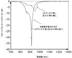
- the IC tag of 1st Embodiment it is a graph which shows the result (comparative example) which analyzed the impedance characteristic of the antenna for UHF in this embodiment tag, when there is no HF antenna, and when there is no IC for HF with a simulator. .
- FIG. 2 It is a figure which shows the structure of the comparison object 2 for comparing with the IC tag of 1st Embodiment. It is the graph which compared the experimental result (actual value) of the impedance characteristic of the antenna for HF in the IC tag of 1st Embodiment, and the comparison objects 1 and 2.
- FIG. 2 It is a figure which shows the structure of the IC tag of 2nd Embodiment. It is a figure which shows the structure of the 1st surface and 2nd surface of the base material of the IC tag of 3rd Embodiment. It is a figure which shows the structure of the 1st surface and 2nd surface of the base material of the IC tag of 4th Embodiment.
- an IC tag that can be used in two communication frequency bands of the UHF band and the HF band is applied to a contactless information communication terminal device, a card-type device, a portable phone, and a wearable device according to the present invention. It is an embodiment in the case of applying.
- the UHF band and the HF band, or the UHF communication system (UHF system) and the HF communication system (HF system) that use the communication band will be described, but the two frequency bands are different. For example, it is not limited to these frequency bands.
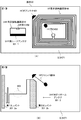
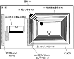
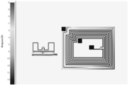
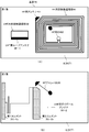
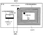
- FIG. 1 is a diagram showing the configuration of the first surface and the second surface of the IC tag 1 in the present embodiment
- FIG. 2 shows the circuit and the second surface of the first surface in the IC tag 1 of the present embodiment. It is a figure which shows these positional relationships.
- the second surface shown in FIG. 1B is in a relation of making the first surface shown in FIG.
- the IC tag 1 of this embodiment includes two non-contact information communication units (circuit units such as an inlay, an inlet, or a chip) that use different frequency bands (for example, an HF band and a UHF band having a higher frequency than the HF band). It is a single structure that transmits and receives signals in a state where two antennas are electrically coupled to each other.
- circuit units such as an inlay, an inlet, or a chip
- the IC tag 1 of the present embodiment increases the effective area of the UHF antenna as viewed from the reader device (not shown), reduces the size of the IC tag 1 itself, and the Q value of each frequency band or The antenna gain can be maintained and improved, and communication efficiency (or distance) and communication accuracy corresponding to signal processing in two frequency bands can be improved without interfering with signal transmission / reception. It is like that.
- the improvement in communication efficiency is remarkable in the case of a high frequency band with a long communication distance such as the UHF band.
- the IC tag 1 of the present embodiment is for UHF used in a UHF communication system that is formed on the base 20 and uses the UHF band.
- a non-contact communication unit (communication method: radio wave) 30 and an HF non-contact communication unit (communication method: magnetic field resonance) 40 formed on the substrate 20 and used in an HF communication system using the HF band are provided. Yes.
- the UHF contactless communication unit 30 receives a signal transmitted from a UHF system reader device (not shown), generates an electromotive force based on the received signal, and uses the electromotive force to generate a reader device. And transmitting and receiving signals.
- the UHF non-contact communication unit 30 includes the UHF loop antenna 301-1 formed on the first surface of the base material 20 and the second of the base material 20, as shown in FIGS.
- the UHF antenna 301 is formed by the UHF dipole antenna 301-2 formed on the surface, and is formed as a single circuit unit (for example, an IC chip) on the first surface and connected to the UHF loop antenna 301-1.
- the UHF loop antenna 301-1 and the UHF dipole antenna 301-2 are formed so as to be electrically coupled to each other via the base material 20, and the UHF antenna 301 transmits and receives a UHF band signal. It functions as a single loop and dipole antenna.
- the UHF dipole antenna 301-2 includes a first element 301-2a and a second element 301-2b formed on the second surface of the base member 20.
- the UHF dipole antenna 301-2 of this embodiment may be replaced with a slit antenna or a vent slot antenna.
- first element 301-2a and the second element 301-2b of the UHF dipole antenna 301-2 of this embodiment are formed of a conductor such as aluminum, for example.
- the HF non-contact communication unit 40 receives a signal transmitted from a reader device for an HF system (not shown), generates an electromotive force based on the received signal, and uses the electromotive force to generate a reader device. And transmitting and receiving signals.
- the HF non-contact communication unit 40 is formed as a single circuit unit (for example, an IC chip) different from the UHF IC 302 on the first surface and the HF antenna 401 formed on the first surface of the substrate 20.
- the HF IC 402 connected to the HF antenna 401 and the HF jumper line 60 formed on the second surface and connecting one end and the other end of the HF antenna 401 are provided.
- the HF jumper wire 60 is formed at a position on the second surface that short-circuits the formation region of the terminal portion of the HF antenna 401. And in order to comprise an HF magnetic field resonance coil, the termination
- FIG. since this point is the same as that of a conventional non-contact information communication terminal device, details are omitted.
- the material of the conductor constituting the HF antenna 401 is arbitrary, in this embodiment, for example, a copper wire, an aluminum foil, a copper foil, a conductive resin, a conductive material are used to reduce the manufacturing cost of the antenna.
- a conductive material such as ink or a metal vapor deposition film is used.
- the HF antenna 401 is formed by copper winding, aluminum etching, or the like.
- the HF antenna 401 and the UHF loop antenna 301-1 are provided in a state of being separated from each other.
- the second element 301-2b of the UHF dipole antenna 301-2 is interposed between the HF antenna 401 and the base material 20 as shown in FIG. It is arranged at the overlapping position.
- the second element 301-2b of the UHF dipole antenna 301-2 is electrically coupled to the HF antenna 401 via the base material 20 to transmit and receive UHF band signals.
- the HF antenna 401 is electrically coupled to the HF antenna 401 via the base material 20 to transmit and receive UHF band signals.
- the UHF loop antenna 301-1, the UHF dipole antenna 301-2, and the HF antenna 401 are electrically coupled, and the overall characteristic impedance in the electrolytic coupling state Is matched with the input impedance of the UHF IC 302 and the HF IC 402.
- the HF jumper wire 60 is insulated from the UHF dipole antenna 301-2.
- the HF antenna 401 can be used for transmission / reception of another antenna unit (that is, the UHF antenna 301), and the UHF antenna 301 and the HF Since the antennas 401 for use can be insulated from each other, the influence of the UHF antenna 301 on transmission / reception of radio waves in the HF antenna 401 (that is, interference with the antenna unit) can be reduced. Yes.
- a hybrid type IC tag having communication systems with different frequency bands such as UHF band and HF band is equipped with a non-contact information communication unit (including an inlay, an inlet, a chip, etc.) corresponding to both communication systems.
- a non-contact information communication unit including an inlay, an inlet, a chip, etc.
- both antennas act as one metal piece when viewed from one antenna, and the antennas in each non-contact information communication unit interfere with each other.
- the effective area of the antenna unit is expanded by two antenna units, and the gain of the transmitted / received signal is maintained while eliminating the influence of other antenna units. And it can be improved.
- the IC tag 1 can reduce the influence of signal reflection and interference and improve communication efficiency even when transmitting and receiving signals while both antennas 301 and 401 are electrically coupled. It is like that.
- the UHF antenna 301 having the UHF loop antenna 301-1 and the UHF dipole antenna 301-2 of the present embodiment constitutes the first antenna unit of the present invention, and the HF antenna 401 is of the present invention.
- a second antenna unit is configured.
- the UHF IC 302 and the HF IC 402 of the present embodiment constitute the first processing circuit or the second processing circuit of the present invention, respectively, and the first element 301-2a and the second processing circuit of the present embodiment.
- Each of the elements 301-2b constitutes a first element or a second element of the present invention.
- the UHF loop antenna 301-1 constitutes the antenna A of the present invention
- the UHF dipole antenna 301-2 constitutes the antenna B of the present invention.
- FIG. 3 is a diagram showing an equivalent circuit of the IC tag 1 of the present embodiment.
- the IC tag 1 of the present embodiment has a first element 301-2a connected to one end side of the UHF loop antenna 301-1 and a second element 301-2b connected to the other end side.
- the UHF antenna 301 and the HF antenna 401 are connected via a capacitor C1 formed by the connected second element 301-2b, the HF antenna 401, and the base material 20 sandwiched between them. Equivalent to connected state.
- the HF antenna 401 is equivalent to an LC circuit composed of an inductor L and a parasitic capacitor C2, and even when transmitting / receiving a UHF band signal, the HF antenna 401-1, Since the antenna 401 is coupled to the electric field via the UHF dipole antenna 301-2 and the base material 20, a part or all of the HF antenna 401 is partly transmitted / received during UHF band signal transmission / reception. It functions as a part of the UHF antenna 301 and can function as one antenna in the combined state.
- the IC tag 1 can increase the effective area of the UHF antenna 301 as viewed from the reader device of the UHF system (not shown) and can increase the gain of the UHF antenna.
- the communication accuracy can be improved while improving the communication range.
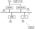
- FIG. 4 is a block diagram showing the configuration of the UHF IC 302 and the HF IIC 402 mounted on the IC tag of this embodiment. Further, since the UHF IC 302 and the HF IC 402 basically have the same configuration, unless otherwise specified, each unit shown in FIG. 4 is common to the UHF IC 302 and the HF IIC 402. It shall have the structure and function.
- the UHF IC 302 and the HF IC 402 are each formed with a processing circuit for receiving a UHF signal or an HF signal and performing other processing. It has the structure which performs an appropriate process according to a use form.
- the UHF IC 302 (HF IC 402) of the present embodiment includes a transmission / reception unit 3001 (see FIG. 4) that mediates transmission / reception of signals between the UHF antenna 301 (HF antenna 401) and the bus B.
- the transmission / reception unit 3001 transmits and receives signals in the frequency band used in the corresponding system, and therefore down-converts the RF (Radio Frequency) signal into a baseband signal, and converts the baseband signal into the RF
- An up-converter that up-converts the signal, a filter circuit, a modulator / demodulator, a DAC (digital / analog converter), and an ADC (analog-digital converter).
- the transmission / reception unit 3001 and the transmission / reception unit 4001 have different circuit configurations in the UHF IC 302 and the HF IC 402 depending on the frequency band (UHF band or HF band) used in the system.
- the electromotive force generation unit 3002 (electromotive force generation unit 4002) generates electromotive force based on the received signal by the transmission / reception unit 3001 (transmission / reception unit 4001) and supplies the generated electromotive force to the bus B.
- Each unit of the UHF IC 302 (HF IC 402) acquires the supplied power from the bus B and uses it as a power source.
- the processing unit 3003 executes predetermined processing according to a protocol defined in the UHF system (HF system).
- HF system UHF system
- the memory 3004 (memory 4004) is a nonvolatile memory having a predetermined recording area, and identification information is recorded in the recording area. Specifically, the identification information recorded in the memory 3004 (memory 4004) is changed as follows according to the purpose of use of the IC tag 1.
- the UHF IC 302 may be disposed at any location on the substrate 20 as long as the impedance with the UHF antenna 301 is matched. For example, in the example of FIG. 1 of the present embodiment, it is arranged at the upper center of the UHF loop antenna 301-1 on the first surface.
- the HF IC 402 may be disposed at any location on the substrate 20 as long as the impedance with the HF antenna 401 is matched. It is desirable that the antenna is disposed at a position spaced a predetermined distance below the center of the antenna.
- article attribute information including a product name, a product number, a manufacturing number, and the like of a target product is recorded as identification information.
- a reader device for example, a gate type.
- Identification information is read from all the IC tags 1 that have been read.
- identification information is read using a reader device (for example, a handy type reader device).
- the IC tag 1 of the present embodiment appropriately switches the communication method to be used between the UHF system or the HF system according to the received signal, It is possible to manage the distribution and production of goods.
- user attribute information including at least a user identification ID (employee number, room number, user ID, etc.) is recorded as identification information.
- a user identification ID employee number, room number, user ID, etc.
- reader devices are installed at the entrances and exits of apartment buildings such as condominiums, the entrances and exits of company buildings, or the gates and other entrances and exits of the parking lots of the apartment houses and office buildings, and the identification information is read and installed at those entrances and exits. It is used as an open / close key for doors and gates, and the HF system is installed at the entrances and exits of individual rooms, floors or parts thereof by reading the identification information. Used as door opening / closing key.
- the IC tag 1 of the present embodiment appropriately switches the communication method to be used between the UHF system or the HF system according to the received signal.
- the IC tag 1 of the present embodiment In addition to preventing unauthorized entry into condominiums and company buildings, it can be used for entering individual rooms, managing employee attendance, and managing individual and employee entry.
- the memory 3004 When used for an electronic wallet or the like, not only the user ID but also electronic money information is recorded as identification information.
- money transfer including not only direct transfer but also indirect transfer using other billing server devices
- a gate type where entry / exit is performed in units of cars such as ETC.
- the user ID and electronic money information are read out.
- the user ID and electronic money information are read when money is exchanged in units of humans such as public transportation.
- the IC tag 1 makes payment at the time of shopping while appropriately switching the communication method to be used between the UHF system or the HF system according to the received signal. It can be used as a prepaid ticket or a prepaid ticket, and can be processed quickly and cashlessly even when the transit time and communication distance such as ETC are long.
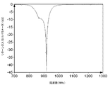
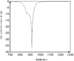
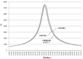
- FIG. 5 is a graph showing the result of analyzing the impedance characteristics of the UHF antenna 301 mounted on the IC tag 1 of the present embodiment by a simulator.
- FIG. 6 is a graph showing the HF antenna in the IC tag 1 of the present embodiment.
- FIG. 7 is a graph showing the result of analyzing the impedance characteristics of the UHF antenna with a simulator when only the HF IC is deleted, and
- FIG. It is a graph which shows the result (comparative example) which analyzed the impedance characteristic of the antenna for UHF by a simulator when there is no antenna and there is no IC for HF.
- FIGS. 5 to 7 show the signal value on the horizontal axis and the dB value (decibel value) of the S11 parameter of the scattering matrix (S matrix) indicating the return loss (reflection loss) in the UHF antenna 301 on the vertical axis. It is a simulation result in the case of.
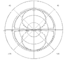
- FIGS. 8 and 9 show, by means of a simulator, the state of change in current density generated on the first surface or the second surface of the base material 20 when a signal of 920 MHz is received by the IC tag 1 of the present embodiment. It is a figure which shows the result.
- FIG. 10 is a diagram showing a result of analyzing the gain of the UHF antenna 301 in the IC tag 1 of the present embodiment by a simulator
- FIG. 11 is a graph showing no HF antenna and HF in the IC tag 1 of the present embodiment. It is a figure which shows the result (comparative example) which analyzed the gain of the antenna for UHF in the case where there is no IC for operation with a simulator.
- FIG. 10 shows the gain of the UHF antenna 301 (that is, the same condition as FIG. 5) when the HF IC 402 having the impedance characteristics shown in FIG. 5 is mounted
- FIG. 11 shows the gain for the HF in FIG. The gain of the UHF antenna 301 when the antenna 301 is not mounted is shown.
- the return loss of the UHF antenna 301 in the vicinity of 900 MHz is about ⁇ 45 dB in the vicinity of 900 MHz regardless of whether or not the HF IC 402 is mounted on the IC tag 1.
- the peak frequency shift due to the presence or absence of the HF IC 402 is not observed, and the amount of change in the return loss is about 5 dB.
- the present invention can be used for transmission / reception of signals in the UHF band regardless of the configuration in which the IC tag 1 is mounted or the configuration in which the IC tag 1 is not mounted. Further, the influence of the HF IC 402 mounted on the IC tag 1 on the transmission / reception of the UHF band signal is very small, and even when the HF IC 402 is mounted, the influence on the transmission / reception of the UHF band signal is small. It can also be confirmed.
- the return loss of the UHF antenna 301 in the vicinity of 900 MHz is about ⁇ 5 dB, and the peak frequency is several tens.
- the return loss peak of the UHF antenna 301 appears in the vicinity of 900 MHz, and the value is also improved to about -40 dB. Can be confirmed.
- the HF antenna 401 electric field coupled to the UHF dipole antenna 301-2 via the base member 20 contributes to the improvement of the return loss value of the UHF antenna 301.
- the UHF loop antenna 301-1 and the HF antenna 401 are coupled via the UHF dipole antenna 301-2. It can also be confirmed. That is, from the current distribution on the second surface, the UHF loop antenna 301-1 is field-coupled to the UHF dipole antenna 301-2 in the region BD, and the second element 301-2b of the UHF dipole antenna 301-2. However, it can be seen that the electric field coupling is performed with the HF antenna 401.
- the HF antenna 401 is short-circuited by the HF jumper line 60 and forms a single circuit including the HF jumper line 60, the HF antenna 401 and the HF jumper line 60 are considered separately. Therefore, even when the UHF frequency is loaded, a current flows through the HF jumper line 60.
- the gain at 920 MHz of the UHF antenna 301 (which combines the UHF loop antenna 301-1 and the UHF dipole antenna 301-2) in the IC tag 1 of the present embodiment is simulated.
- the result shown in FIG. 10 was obtained, and as a result, it was confirmed that the gain of the UHF antenna 301 can be secured to about 1.04 dBi in the IC tag 1 of the present embodiment.
- the gain of the UHF antenna 301 was simulated for a sample in which the HF antenna 401 was deleted from the IC tag 1, and FIG. As a result, it was found that the gain of the UHF antenna 301 can be secured only by about -1.09 dBi.
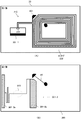
- FIG. 12 and 13 are diagrams showing the configuration of the comparison object 1 or the comparison object 2 for comparison with the IC tag 1 of the present embodiment
- FIG. 14 is a comparison object of the IC tag 1 of the present embodiment and the comparison object.
- 6 is a graph comparing experimental results (actual measurement values) of impedance characteristics of HF antennas in 1 and 2;
- the result of this experiment is that the IC tag 1 of this embodiment and the prototype 1 of the comparison object 1 or the comparison object 2 are created and the IC tag 1 created using the impedance analyzer (HP 4294A manufactured by Agilent Technologies) and the comparison object 1 Alternatively, the absolute value ( ⁇ ), the voltage Vs, and the phase ⁇ of the impedance Z in the comparison object 2 are measured.
- the impedance analyzer HP 4294A manufactured by Agilent Technologies
- (Expression 1) is an expression for calculating the Q value in the parallel equivalent circuit
- (Expression 2) is an expression for calculating the Q value in the series equivalent circuit.
- the comparison target 1 is an IC tag in which the UHF IC 302 is deleted from the IC tag 1 of the present embodiment, that is, a sample in which only the UHF IC 302 is deleted from the IC tag 1 of the present embodiment.
- the comparison target 2 is an IC tag in which the UHF non-contact communication unit 30 is deleted from the IC tag 1 of this embodiment, that is, the UHF loop antenna 301-1 and the UHF IC 302 from the IC tag 1 of this embodiment. This is a deleted sample.
- FIG. 14 shows the experimental results for the characteristic impedances of the comparison target 1 and the comparison target 2 configured as described above and the IC tag 1 of the present embodiment.
- the horizontal axis represents frequency
- the vertical axis represents
- comparison target 1 and the comparison target 2 the actual measurement value of the resonance frequency in the IC tag 1 of the present embodiment, the calculation result based on the equivalent circuit of R1, C1, and L1, and the calculation result of the Q value calculated from these It is shown in Table 1 (in the case of the parallel equivalent circuit of Equation 1).
- the resistance (value) L calculated by the program inside the device when the equivalent circuit is selected when the IC tag 1, the comparison target 1 or the comparison target 2 is measured by the impedance analyzer.
- a capacitor (capacitance) C and a coil (inductance) are used.
- the characteristics of the HF antenna in the IC tag 1 of this embodiment and the comparison target 1 are almost overlapped, and a peak (that is, a resonance frequency) appears in the vicinity of 16.4 MHz for both. Little frequency shift or magnitude change has been observed.
- the Q value of the HF antenna 401 in the IC tag 1 of the present embodiment is 25.5
- the Q value of the HF antenna in the comparison target 1 is 25.6
- the rate of change is about 0.4. It can be seen from this that the antenna characteristics of the IC tag 1 and the comparison object 1 are almost the same.
- the characteristics of the HF antennas in the IC tag 1 and the comparison object 2 of the present embodiment are slight, but the peak frequency shift occurs, but the change does not affect the signal reception. I understand.
- the Q value of the HF antenna 401 in the IC tag 1 of the present embodiment is 25.5
- the Q value of the HF antenna in the comparison target 2 is 26.0
- the rate of change is about 2.0. From this, it can be seen that the antenna characteristic in the comparison target 2 is not a change that affects signal reception.
- the IC tag 1 of the present embodiment is provided with the UHF non-contact communication unit 30 and the HF non-contact communication unit 40 on the first surface of the base material 20, and the UHF antenna 301 (UHF loop).
- the antenna 301-1 and the UHF dipole antenna 301-2) and the HF antenna 401 are arranged at positions separated from each other on the first surface, and the UHF antenna 301 and the HF antenna are received when receiving the UHF signal. Since 401 are configured to be coupled to each other through a UHF dipole antenna 301-2 formed on the second surface of the substrate 20, a part of the HF antenna 401 is transmitted and received in the UHF band.
- the effective area of the UHF antenna 301 viewed from the reader device is improved, and the gain is maintained and improved. Theft is possible.
- the IC tag 1 of the present embodiment has two or more non-contact information communication terminal devices (that is, UHF non-contact communication units 30 and 30) that use different frequency bands (that is, UHF band and HF band), respectively. Even when the HF non-contact communication unit 40) is mounted, the gain of the UHF antenna 301 is maintained and improved, and the communication in different frequency bands is realized well while preventing the IC tag from becoming large. can do.
- UHF non-contact communication unit 40 Even when the HF non-contact communication unit 40) is mounted, the gain of the UHF antenna 301 is maintained and improved, and the communication in different frequency bands is realized well while preventing the IC tag from becoming large. can do.
- FIG. 15 is a diagram showing the configuration of the IC tag 10 of the second embodiment.
- the same components as those in FIG. 1 are denoted by the same reference numerals.
- the IC tag 10 of the present embodiment has a UHF non-contact communication unit 30 and an HF non-contact communication unit on the first surface of the base material 20, similar to the IC tag 1 of the first embodiment. 40 are spaced apart from each other, and a space A is provided between the UHF non-contact communication unit 30 and the HF non-contact communication unit 40.
- the separation distance indicating the space A is preferably 0.5 mm or less.
- the UHF dipole antenna 301-2 is not provided on the second surface of the substrate 20 of the IC tag 10 of the present embodiment. That is, the IC tag 10 of the embodiment has a configuration in which the UHF dipole antenna 301-2 is excluded from the IC tag 1 of the first embodiment.
- the HF jumper wire 60 is provided although not particularly shown.
- the UHF loop antenna 301-1 and the HF antenna 401 are configured to be coupled to each other through the space A.
- the IC tag 10 uses a part of the HF antenna 401 for transmission / reception of a UHF band signal, improves the effective area as viewed from the reader device of the UHF antenna 301, and maintains the gain. It becomes possible to improve.
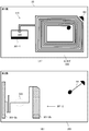
- FIG. 16 is a diagram illustrating the configuration of the first surface and the second surface of the IC tag in the present embodiment.
- the same components as those in FIG. 1 are denoted by the same reference numerals.
- the IC tag 100 of the present embodiment is arranged with the HF antenna 401 and the HF IC 402 formed on the first surface of the substrate 20, and the second of the substrate 20.
- a UHF loop antenna 301-1, a UHF dipole antenna 301-2, and a UHF IC 302 are formed and arranged.
- the UHF loop antenna 301-1 and the UHF dipole antenna 301-2 and the HF antenna 401 are configured to be electrically coupled to each other through the substrate 20.
- the UHF dipole antenna 301-2 includes a first element 301-2a and a second element 301-2b.
- the IC tag 100 of the present embodiment has two or more non-contact information communication terminal devices (that is, UHF non-contact communication units 30) that use different frequency bands (that is, UHF band and HF band), respectively. Even when the HF non-contact communication unit 40) is mounted, the gain of the UHF loop antenna 301-1 is improved, and the IC tag is prevented from becoming large, and communication in different frequency bands is improved. Can be realized.
- FIG. 17 is a diagram illustrating the configuration of the first surface and the second surface of the IC tag according to the present embodiment
- FIG. 18 illustrates the configuration of the first surface and the second surface of the IC tag according to the present embodiment. It is the other example of a figure.
- each of the UHF non-contact communication unit 30 and the HF non-contact communication unit 40 is provided in an individual IC having processing circuits such as a transmission / reception unit and a processing unit.
- the UHF processing circuit and the HF communication system processing circuit are formed by an IC (hereinafter referred to as “hybrid IC”) as a single circuit unit.
- the configuration of the present embodiment has the same configuration as that of the first embodiment except for the above points, and the same members are denoted by the same reference numerals and description thereof is omitted. Moreover, except for the IC, each antenna is arranged at the same position as in the first embodiment.
- the IC tag 200 As shown in FIGS. 17A and 17B, the IC tag 200 according to the present embodiment is formed on a base material 20 and the base material 20, and uses a UHF communication system and a UHF / HF non-HF communication system.
- a contact communication unit 210 As shown in FIGS. 17A and 17B, the IC tag 200 according to the present embodiment is formed on a base material 20 and the base material 20, and uses a UHF communication system and a UHF / HF non-HF communication system.
- a contact communication unit 210 A contact communication unit 210.
- the UHF / HF non-contact communication unit 210 is formed on the base material 20, the UHF antenna 301 formed on the base material 20 and used in the UHF communication system, and HF communication. It has an HF antenna 401 used in the system, and a hybrid IC 220 formed by a single circuit unit, each processing circuit used in the UHF communication system and the HF communication system.
- the hybrid IC 220 includes a transmission / reception unit 3001 for an UHF communication system, an electromotive force generation unit 3002, a processing unit 3003 and a memory 3004, a transmission / reception unit 4001 for an HF communication system, an electromotive force generation unit 4002, A processing unit 4003 and a memory 4004 are included.
- the UHF antenna 301 and the HF antenna 401 are separated and connected by an internal resistance.
- the hybrid IC 220 is located on the base material 20 at a position in contact with both the UHF loop antenna 301-1 and the HF antenna 401 of the UHF antenna 301 on the assumption that the impedance is matched. If it is mounted, the mounting position is not limited.
- hybrid IC 220 the allowable range of the position when the mounting position is determined based on impedance matching with UHF antenna 301 is greater than the position when the mounting position is determined based on impedance matching with HF antenna 401. Since it is narrow, the hybrid IC 220 is arranged at an appropriate mounting position in the UHF loop antenna 301-1, such as the center of the upper part of the UHF loop antenna 301-1, as in the UHF IC 302 of the first embodiment. It is desirable to connect to the HF antenna 401 at a position.
- the IC tag 200 of the present embodiment has two or more non-contact information communication terminal devices (that is, UHF non-contact communication units 30) that use different frequency bands (that is, UHF band and HF band), respectively.
- the HF non-contact communication unit 40 can be configured using a hybrid IC 220 which is a single circuit unit.
- the IC tag 200 of this embodiment improves the gain of the UHF loop antenna 301-1 to prevent the IC tag from becoming large, and the number of ICs is reduced, thereby simplifying the manufacturing process and easily. Can be manufactured.
- the winding method of the HF antenna 401 may be changed, and although not shown, the arrangement position and direction of the loop of the UHF loop antenna 301-1 are not limited.
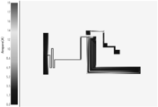
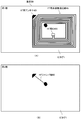
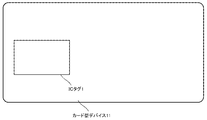
- Modification 1 In the above embodiment, the IC tag 1 has been described as an example. However, as shown in FIG. 19, the IC tag 1 is mounted on a card-like housing and used as the card type device 11. Also good.
- FIG. 19 is a diagram showing a configuration of the card type device 11 of the first modification.
- information about the user such as an employee number can be recorded in the memory 3004 of the HF IC 402 and used as an employee ID card, which can be used for attendance management and room entry management. . It is also possible to record information about electronic money in the memory 3004 and use it as a prepaid ticket in public transportation.
- IC tag you may use not only 1st Embodiment but IC tag of 2nd Embodiment or 3rd Embodiment.
- the electronic money reduction processing in this case is the same as that of the conventional HF system, and thus the details are omitted.
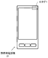
- FIG. 20 is a diagram illustrating a configuration of the mobile phone 21 according to the second modification.
- the IC tag not only the first embodiment but also the IC tag of the second embodiment or the third embodiment may be used. Further, the NFC function in this case is the same as the conventional function, and the details are omitted.
- FIG. 21 is a diagram illustrating a configuration of a wearable device (wristband) 31 according to the third modification.
- information related to an admission ticket, concert ticket, ski lift use ticket, etc. is recorded in the memory 3004, and the information is read out by using a reader device at the admission gate etc. It can be used to prevent entry of users who do not have it.
- the UHF system and the non-contact information communication unit in the HF system are provided, and the IC tag 1 that transmits and receives signals in a state where the antennas of the respective systems are electrically coupled to each other will be described.
- a UHF system and an LF (Low Frequency) communication system communication method: magnetic resonance
- a UHF system having a frequency different from that of the UHF system is provided with a non-contact type information communication unit.
- an IC tag that transmits and receives signals in a state where electric fields are mutually coupled.
- an IC tag that provides two non-contact information communication units using two different frequency bands and transmits and receives signals in a state where the two antennas are electrically coupled to each other.
- an IC tag that provides three or more non-contact information communication units using three or more different frequency bands and transmits and receives signals in a state where the three antennas are electrically coupled to each other. Is also applicable.
- non-contact information communication units in three different communication systems such as HF system, UHF system and LF system, or three non-contact information communication units consisting of two UHF systems and HF systems with different frequencies are provided.
- the present invention can also be applied to an IC tag that transmits and receives signals in a state where the three antennas are electrically coupled to each other.
Landscapes
- Engineering & Computer Science (AREA)
- Signal Processing (AREA)
- Computer Networks & Wireless Communication (AREA)
- Physics & Mathematics (AREA)
- General Physics & Mathematics (AREA)
- Theoretical Computer Science (AREA)
- Microelectronics & Electronic Packaging (AREA)
- Computer Hardware Design (AREA)
- Near-Field Transmission Systems (AREA)
- Details Of Aerials (AREA)
- Transceivers (AREA)
- Variable-Direction Aerials And Aerial Arrays (AREA)
- Support Of Aerials (AREA)
Abstract
Description
(1)UHF(Ultra High Frequency)帯の信号(例えば、920MHz帯又は2.45GHz帯の信号)を利用する通信方式のシステム(以下、「UHFシステム」という。)(例えば、特許文献1)と、
(2)HF(High Freqeuncy)帯の信号(例えば、13.5MHz帯の信号)を利用する通信方式のシステム(以下、「HFシステム」という。)(例えば、特許文献2)と、
が存在する。
[1.1]ICタグの概要
まず、図1及び図2を用いつつ、本実施形態のICタグ1の概要及び構成について説明する。なお、図1は、本実施形態におけるICタグ1の第1面及び第2面の構成を示す図であり、図2は、本実施形態のICタグ1における第1面の回路と第2面の位置関係を示す図である。また、図1(B)に示す第2面は、基材20において、図1(A)に示す第1面と表裏をなす関係にある。
次に、図3を用いて本実施形態のICタグ1の概要及び構成について説明する。なお、図3は、本実施形態のICタグ1の等価回路を示す図である。
次に、図4を用いて本実施形態におけるICタグ1に搭載されるUHF用IC302及びHF用IC402について説明する。
メモリ3004(メモリ4004)には、対象となる物品の品名、品番、製造番号等を含む物品属性情報が識別情報として記録される。特に、UHFシステムの場合には、大量の物品が流れ作業的に移動する際に(例えば、物品が工場から出荷される際に)、リーダ装置(例えば、ゲート型)により、出荷対象物品に添付された全てのICタグ1から識別情報が読み出される。また、HFシステムの場合には、物品が店舗に納品された際に、リーダ装置(例えば、ハンディタイプのリーダ装置)を用いて識別情報が読み出される。
メモリ3004(メモリ4004)には、ユーザの識別ID(社員番号、部屋番号、ユーザID等)を少なくとも含むユーザ属性情報を識別情報として記録される。例えば、UHFシステムについては、マンションなどの集合住宅の出入り口や社屋の出入り口又は当該集合住宅や社屋の駐車場のゲートその他の出入り口にリーダ装置を設け、識別情報を読み出すことによってそれらの出入り口に設置されているドアやゲートの開閉キーとして利用するとともに、HFシステムについては、個別の部屋、フロア又はその一部などの出入り口にリーダ装置を設け、識別情報を読み出すことによってそれらの出入り口に設置されているドアの開閉キーとして用いられる。
メモリ3004(メモリ4004)には、識別情報として、ユーザIDのみならず、電子マネー情報が記録される。特に、UHFシステムの場合には、ETCなどの自動車単位で入退場を行うゲート式における金銭の授受(直接的な授受だけなく、他の課金サーバ装置を用いた間接的な授受を含む)を行う際に、ユーザIDや電子マネー情報が読み出される。また、HFシステムの場合には、公共交通機関などの人間単位で金銭の授受を行う際にユーザID及び電子マネー情報が読み出される。
[1.4.1]UHF用アンテナの通信特性(シミュレーション)
次に、図5~図11を用いて本実施形態のICタグ1におけるUHF用ループアンテナ301-1とUHF用ダイポールアンテナ301-2とから構成されるUHF用アンテナ301の通信特性のシミュレーション結果について説明する。
次に、図12~図14を用いて本実施形態のICタグ1におけるHF用アンテナ401の通信特性の実験結果(実測値)について説明する。

次に、図15を用いて本発明に係る非接触式情報通信端末装置の第2実施形態について説明する。なお、図15は、第2実施形態のICタグ10の構成を示す図であり、図15において、図1と同様の構成要素については、同様の符号を付してある。
次に、図16を用いて本発明に係る非接触式情報通信端末装置の第3の実施形態について説明する。なお、図16は、本実施形態におけるICタグの第1面及び第2面の構成を示す図である。また、図16において、図1と同様の構成要素には同一の符号を付してある。
次に、図17及び18を用いて本発明に係る非接触式情報通信端末装置の第4の実施形態について説明する。なお、図17は、本実施形態におけるICタグの第1面及び第2面の構成を示す図であり、図18は、本実施形態におけるICタグの第1面及び第2面の構成を示す図のその他の例である。
[5.1]変形例1
また、上記実施形態においては、ICタグ1を例に説明を行ったが、図19に示すようにICタグ1をカード状の筐体に搭載して、カード型デバイス11として利用するようにしてもよい。なお、図19は変形例1のカード型デバイス11の構成を示す図である。
また、上記実施形態においては、ICタグを例に説明を行ったが、図20に示すように、ICタグ1を携帯用電話機21の筐体内に搭載して、携帯用電話機21のNFC機能に利用することも可能である。なお、図20は、変形例2の携帯用電話機21の構成を示す図である。
また、上記実施形態においては、ICタグを例に説明を行ったが、図21に示すように、ICタグ1をリストバンド、ネックストラップ、眼鏡等に搭載して、ウェアラブルデバイス31を構成することも可能である。なお、図21は、変形例3のウェアラブルデバイス(リストバンド)31の構成を示す図である。
また、本実施形態においては、UHFシステムとHFシステムにおける非接触式情報通信部を設け、それぞれのシステムのアンテナを相互に電界結合させた状態にて信号の送受信を行うICタグ1を用いて説明したが、UHFシステムと125KHzなどのLF(Low Frequency)通信システム(通信方式:磁界共振)、又は、UHFシステムと異なる周波数のUHFシステムにおける非接触式情報通信部を設け、それぞれのシステムのアンテナを相互に電界結合させた状態にて信号の送受信を行うICタグについても提供する可能である。
11 … カード型デバイス
20 … 基材
21 … 携帯用電話機
30 … UHF用非接触通信部
31 … ウェアラブルデバイス
40 … HF用非接触通信部
210 … UHF/HF用非接触通信部
220 … ハイブリッドIC
301-1 … UHF用ループアンテナ
301-2 … UHF用ダイポールアンテナ
301-2a … 第1エレメント
301-2b … 第2エレメント
302 … UHF用IC
401 … HF用アンテナ
402 … HF用IC
3001、4001 … 送受信部
3002、4002 … 起電力発生部
3003、4003 … 処理部
3004、4004 … メモリ
Claims (18)
- 通信を行う際の周波数が異なる複数の通信装置との信号の送受信を非接触にて行う非接触式情報通信端末装置であって、
基材と、
前記基材上に形成された第1の周波数を有する第1の信号を送受信する第1のアンテナユニットと、
前記第1のアンテナユニットに接続されるとともに、前記第1のアンテナユニットにより前記第1の信号が受信された場合に、当該第1の信号に基づき、予め定められた第1の処理を実行し、当該処理結果に対応する信号を第1の処理信号として、前記第1のアンテナユニットに出力する第1の処理回路と、
前記基材上に形成された前記第1の周波数とは異なる第2の周波数を有する第2の信号を送受信する第2のアンテナユニットと、
前記第2のアンテナユニットに接続されるとともに、前記第2のアンテナユニットによって前記第2の信号が受信された場合に、当該第2の信号に基づき、予め定められた第2の処理を実行し、当該処理結果に対応する信号を第2の処理信号として、前記第2のアンテナユニットに出力する第2の処理回路と、
を有し、
前記第1のアンテナユニット及び前記第2のアンテナユニットが、互いに絶縁されているとともに、相互に電界結合していることを特徴とする非接触式情報通信端末装置。 - 請求項1に記載の非接触式情報通信端末装置において、
前記第1のアンテナユニットが、アンテナAと当該アンテナAと異なる種類のアンテナBとを有する、非接触式情報通信端末装置。 - 請求項1又は2に記載の非接触式情報通信端末装置において、
前記第1の処理回路及び前記第2の処理回路が、各々、第1のアンテナユニット又は第2のアンテナユニットによって受信した信号に基づき、起電力を発生させ、当該起電力に基づいて該当する処理を実行する、非接触式情報通信端末装置。 - 請求項1~3のいずれか1項に記載の非接触式情報通信端末装置において、
前記第1のアンテナユニットの少なくとも一部と前記第2のアンテナユニットとが、前記基材における同一の面上に離間して形成されるとともに、当該離間した空間を介して、相互に電界結合している、非接触式情報通信端末装置。 - 請求項1~3のいずれか1項に記載の非接触式情報通信端末装置において、
前記第1のアンテナユニットの一部と前記第2のアンテナユニットとが、前記基材における第1面に離間して形成されるとともに、
前記第1のアンテナユニットの他の一部が、前記第1面と異なる第2面に形成され、
前記第1のアンテナユニットの他の一部と第2のアンテナユニットが、前記基材を介して電界結合している、非接触式情報通信端末装置。 - 請求項5に記載の非接触式情報通信端末装置において、
前記第1のアンテナユニットの他の一部が、第1エレメントと第2エレメントを有するダイポールアンテナであり、
前記ダイポールアンテナの第2エレメントと前記第2のアンテナユニットとが前記基板を介して重なっている、非接触式情報通信端末装置。 - 請求項6に記載の非接触式情報通信端末装置において、
前記ダイポールアンテナの第2エレメントが、前記第2のアンテナユニットの一部と前記基板を介して重なっている、非接触式情報通信端末装置。 - 請求項3~7のいずれか1項に記載の非接触式情報通信端末装置において、
前記基材が、フレキシブルなシートによって形成される、非接触式情報通信端末装置。 - 請求項1~8のいずれか1項に記載の非接触式情報通信端末装置において
前記第1のアンテナユニット及び第2のアンテナユニットを電界結合した状態における全体の特性インピーダンスが、前記第1の処理回路、又は、第2の処理回路における入力インピーダンスに整合している、非接触式情報通信端末装置。 - 請求項1~9のいずれか1項に記載の非接触式情報通信端末装置において、
前記第1の処理回路及び第2の処理回路の少なくとも一方が、
自機を他の非接触式情報通信端末装置から識別するための識別情報を記録する記録手段と、
前記第1のアンテナユニット又は第2のアンテナユニットによって前記信号が受信された場合に、前記記録手段から識別情報を読み出し、自回路に接続されたアンテナユニットから当該識別情報の信号を出力する制御部と、
を備える、非接触式情報通信端末装置。 - 請求項10に記載の非接触式情報通信端末装置において、
前記識別情報には、自機が形成された物品又は装置に関する情報が少なくとも含まれる、非接触式情報通信端末装置。 - 請求項10又は11に記載の非接触式情報通信端末装置において、
前記識別情報には、少なくとも自機が組み込まれたデバイスを利用するユーザに関する情報が含まれる、非接触式情報通信端末装置。 - 請求項12に記載の非接触式情報通信端末装置において、
前記ユーザに関する情報には、当該ユーザが、決済を行う際に用いるマネー情報が含まれる、非接触式情報通信端末装置。 - 請求項1~13のいずれか1項に記載の非接触式情報通信端末装置において、
前記第1の処理回路と前記第2の処理回路とが単一の回路ユニットに形成されている、非接触式情報通信端末装置。 - 請求項14に記載の非接触式情報通信端末装置において、
前記第1の周波数が、前記第2の周波数より高周波数であり、
前記回路ユニットが、
前記第2のアンテナユニットより前記第1のアンテナユニットに近接して配置される、非接触式情報通信端末装置。 - 請求項1~15のいずれか1項に記載の非接触式情報通信端末装置を備えるカード型デバイス。
- 請求項1~15のいずれか1項に記載の非接触式情報通信端末装置を備える、携帯用電話機。
- 請求項1~15のいずれか1項に記載の非接触式情報通信端末装置を備える、ウェアラブルデバイス。
Priority Applications (4)
| Application Number | Priority Date | Filing Date | Title |
|---|---|---|---|
| EP15837284.7A EP3196808B1 (en) | 2014-09-01 | 2015-08-31 | Contactless information communication terminal unit, card-type device, portable telephone, and wearable device |
| US15/507,194 US9960814B2 (en) | 2014-09-01 | 2015-08-31 | Contactless information communication terminal unit, card-type device, portable telephone, and wearable device |
| JP2016546536A JP6007356B2 (ja) | 2014-09-01 | 2015-08-31 | 非接触式情報通信端末装置、カード型デバイス、携帯用電話機及びウェアラブルデバイス |
| CN201580046220.0A CN106663217B (zh) | 2014-09-01 | 2015-08-31 | 非接触式信息通信终端装置、卡型设备、携带电话机以及可穿戴式设备 |
Applications Claiming Priority (2)
| Application Number | Priority Date | Filing Date | Title |
|---|---|---|---|
| JP2014-177529 | 2014-09-01 | ||
| JP2014177529 | 2014-09-01 |
Publications (1)
| Publication Number | Publication Date |
|---|---|
| WO2016035771A1 true WO2016035771A1 (ja) | 2016-03-10 |
Family
ID=55439832
Family Applications (1)
| Application Number | Title | Priority Date | Filing Date |
|---|---|---|---|
| PCT/JP2015/074767 WO2016035771A1 (ja) | 2014-09-01 | 2015-08-31 | 非接触式情報通信端末装置、カード型デバイス、携帯用電話機及びウェアラブルデバイス |
Country Status (5)
| Country | Link |
|---|---|
| US (1) | US9960814B2 (ja) |
| EP (1) | EP3196808B1 (ja) |
| JP (2) | JP6007356B2 (ja) |
| CN (1) | CN106663217B (ja) |
| WO (1) | WO2016035771A1 (ja) |
Cited By (6)
| Publication number | Priority date | Publication date | Assignee | Title |
|---|---|---|---|---|
| WO2018034449A1 (ko) * | 2016-08-17 | 2018-02-22 | 주식회사 아이씨케이 | 비접촉식 카드 기능을 갖는 메탈 카드 및 그에 사용되는 금속판과 금속판 조립체, 그리고 그 제조 방법 |
| JP2019035180A (ja) * | 2017-08-15 | 2019-03-07 | 達雄 西岡 | 電子マネーチップを内蔵した光る抗菌性リストバンド類 |
| WO2019054404A1 (ja) * | 2017-09-12 | 2019-03-21 | 株式会社村田製作所 | 無線通信デバイス |
| JP2019091137A (ja) * | 2017-11-13 | 2019-06-13 | 日本エレクトロニクス・サービス株式会社 | Icタグ及びこれを用いた複合型icカード |
| JP2020027646A (ja) * | 2018-08-09 | 2020-02-20 | Nes株式会社 | Icタグ及び複合型icカード |
| JP2020087065A (ja) * | 2018-11-28 | 2020-06-04 | 株式会社マーケテック | 無線通信端末 |
Families Citing this family (14)
| Publication number | Priority date | Publication date | Assignee | Title |
|---|---|---|---|---|
| US10929835B2 (en) | 2013-08-13 | 2021-02-23 | Neology, Inc. | Detachable radio frequency identification switch tag |
| FR3035993B1 (fr) * | 2015-05-06 | 2017-06-09 | Centre Nat Rech Scient | Dispositif d'alarme sans fil miniaturise |
| US11403506B2 (en) | 2015-05-21 | 2022-08-02 | Neology, Inc. | Detachable radio frequency identification switch tag |
| KR102471235B1 (ko) * | 2015-09-04 | 2022-11-28 | 엘지전자 주식회사 | 와치 타입의 이동 단말기 |
| BR112020002362A2 (pt) | 2017-08-04 | 2020-09-08 | Global Battery Solutions Llc | sistema e método do monitor de bateria |
| CN211655071U (zh) | 2017-10-20 | 2020-10-09 | 株式会社村田制作所 | 卡式无线通信设备 |
| DE102018212594B4 (de) * | 2018-07-27 | 2021-11-18 | Textilma Ag | Dualbandtransponder und textiles Etikett mit Dualbandtransponder |
| WO2020097392A1 (en) | 2018-11-07 | 2020-05-14 | Neology, Inc. | Detachable radio frequency identification switch tag |
| JP7145115B2 (ja) * | 2019-03-28 | 2022-09-30 | トッパン・フォームズ株式会社 | Rfidメディア |
| JP7289213B2 (ja) * | 2019-03-28 | 2023-06-09 | ニデックインスツルメンツ株式会社 | カード発行装置 |
| US10997483B2 (en) * | 2019-06-12 | 2021-05-04 | Stmicroelectronics, Inc | NFC antenna switch |
| US10855335B1 (en) * | 2019-09-26 | 2020-12-01 | Amazon Technologies, Inc. | Ring-shaped devices with combined bluetooth and near-field communication antenna assemblies |
| TWI762894B (zh) * | 2019-11-05 | 2022-05-01 | 友達光電股份有限公司 | 電路裝置 |
| US11677151B2 (en) * | 2020-09-11 | 2023-06-13 | Nxp B.V. | Near-field communications device |
Citations (4)
| Publication number | Priority date | Publication date | Assignee | Title |
|---|---|---|---|---|
| WO2009110382A1 (ja) * | 2008-03-03 | 2009-09-11 | 株式会社村田製作所 | 複合アンテナ |
| JP2012016062A (ja) * | 2008-07-02 | 2012-01-19 | Mitsubishi Electric Corp | 無線通信装置 |
| JP2012506079A (ja) * | 2008-10-20 | 2012-03-08 | スマートラック アイピー ビー.ヴィー. | トランスポンダ装置 |
| JP2012108843A (ja) * | 2010-11-19 | 2012-06-07 | Toppan Printing Co Ltd | Rfidタグ |
Family Cites Families (8)
| Publication number | Priority date | Publication date | Assignee | Title |
|---|---|---|---|---|
| US20140071818A1 (en) * | 2004-07-16 | 2014-03-13 | Virginia Innovation Sciences, Inc. | Method and system for efficient communication |
| WO2007098424A2 (en) * | 2006-02-17 | 2007-08-30 | Qualcomm Incorporated | System and method for multi-processor application support |
| JP5267463B2 (ja) | 2008-03-03 | 2013-08-21 | 株式会社村田製作所 | 無線icデバイス及び無線通信システム |
| WO2010001469A1 (ja) * | 2008-07-02 | 2010-01-07 | 三菱電機株式会社 | 無線通信装置 |
| US20110090060A1 (en) * | 2009-10-16 | 2011-04-21 | Tavshikar Milind M | Isolating RFID Reader |
| US8666895B2 (en) * | 2011-01-31 | 2014-03-04 | Bank Of America Corporation | Single action mobile transaction device |
| US9324020B2 (en) * | 2012-08-30 | 2016-04-26 | Nxp B.V. | Antenna structures and methods for omni directional radiation patterns |
| US8903378B2 (en) * | 2013-01-24 | 2014-12-02 | Kunal Shah | Object navigation |
-
2015
- 2015-08-31 CN CN201580046220.0A patent/CN106663217B/zh active Active
- 2015-08-31 WO PCT/JP2015/074767 patent/WO2016035771A1/ja active Application Filing
- 2015-08-31 EP EP15837284.7A patent/EP3196808B1/en active Active
- 2015-08-31 JP JP2016546536A patent/JP6007356B2/ja active Active
- 2015-08-31 US US15/507,194 patent/US9960814B2/en active Active
-
2016
- 2016-09-12 JP JP2016177952A patent/JP6616753B2/ja active Active
Patent Citations (4)
| Publication number | Priority date | Publication date | Assignee | Title |
|---|---|---|---|---|
| WO2009110382A1 (ja) * | 2008-03-03 | 2009-09-11 | 株式会社村田製作所 | 複合アンテナ |
| JP2012016062A (ja) * | 2008-07-02 | 2012-01-19 | Mitsubishi Electric Corp | 無線通信装置 |
| JP2012506079A (ja) * | 2008-10-20 | 2012-03-08 | スマートラック アイピー ビー.ヴィー. | トランスポンダ装置 |
| JP2012108843A (ja) * | 2010-11-19 | 2012-06-07 | Toppan Printing Co Ltd | Rfidタグ |
Cited By (8)
| Publication number | Priority date | Publication date | Assignee | Title |
|---|---|---|---|---|
| WO2018034449A1 (ko) * | 2016-08-17 | 2018-02-22 | 주식회사 아이씨케이 | 비접촉식 카드 기능을 갖는 메탈 카드 및 그에 사용되는 금속판과 금속판 조립체, 그리고 그 제조 방법 |
| JP2019035180A (ja) * | 2017-08-15 | 2019-03-07 | 達雄 西岡 | 電子マネーチップを内蔵した光る抗菌性リストバンド類 |
| WO2019054404A1 (ja) * | 2017-09-12 | 2019-03-21 | 株式会社村田製作所 | 無線通信デバイス |
| JPWO2019054404A1 (ja) * | 2017-09-12 | 2019-11-07 | 株式会社村田製作所 | 無線通信デバイス |
| JP2019091137A (ja) * | 2017-11-13 | 2019-06-13 | 日本エレクトロニクス・サービス株式会社 | Icタグ及びこれを用いた複合型icカード |
| JP2020027646A (ja) * | 2018-08-09 | 2020-02-20 | Nes株式会社 | Icタグ及び複合型icカード |
| JP7356659B2 (ja) | 2018-08-09 | 2023-10-05 | Nes株式会社 | Icタグ及び複合型icカード |
| JP2020087065A (ja) * | 2018-11-28 | 2020-06-04 | 株式会社マーケテック | 無線通信端末 |
Also Published As
| Publication number | Publication date |
|---|---|
| JP6616753B2 (ja) | 2019-12-04 |
| JP2017034686A (ja) | 2017-02-09 |
| US9960814B2 (en) | 2018-05-01 |
| JP6007356B2 (ja) | 2016-10-12 |
| US20170195009A1 (en) | 2017-07-06 |
| EP3196808A4 (en) | 2017-09-13 |
| EP3196808A1 (en) | 2017-07-26 |
| EP3196808B1 (en) | 2019-10-02 |
| CN106663217A (zh) | 2017-05-10 |
| CN106663217B (zh) | 2019-11-05 |
| JPWO2016035771A1 (ja) | 2017-04-27 |
Similar Documents
| Publication | Publication Date | Title |
|---|---|---|
| JP6616753B2 (ja) | 非接触式情報通信端末装置、カード型デバイス、携帯用電話機及びウェアラブルデバイス | |
| US8508429B2 (en) | Radio communication equipment | |
| US20180138746A1 (en) | Combo Antenna Unit And Wireless Power Receiving Module Comprising Same | |
| CN104518283B (zh) | 用于微型化应用的多频天线 | |
| CN201830251U (zh) | 一种近场通信天线装置及手持终端设备 | |
| JP2014157618A (ja) | 可搬型消費者デバイスのシールディング | |
| KR101277556B1 (ko) | 무선 통신장치 | |
| CN102122753A (zh) | 近场通信电子装置及其天线 | |
| JP5020161B2 (ja) | 無線通信装置 | |
| TW201347295A (zh) | 適用於無線射頻識別標籤的不連續迴圈天線,及相關的元件、系統以及方法 | |
| CN102576927B (zh) | 例如用于rfid应答器系统的天线结构 | |
| KR101485569B1 (ko) | 금속 덮개가 적용된 이동통신 단말기의 nfc 안테나 | |
| KR101291044B1 (ko) | 휴대 단말용 안테나 모듈 | |
| TW200949706A (en) | Container and wireless tag reading system | |
| EP2490294B1 (en) | Transmission/reception antenna and transmission/reception device using same | |
| WO2006078147A1 (en) | Thin rfid tag for radio frequency identification | |
| US10741926B2 (en) | Slot antenna structure for electronic tag | |
| WO2006088422A1 (en) | Antenna device for a portable radio communication device | |
| JP2011128956A (ja) | 無線通信装置 | |
| KR100976326B1 (ko) | 다중 루프형 무선인식(rfid) 태그 안테나 및 이를이용한 rfid 태그 | |
| Chiu et al. | Broadband T‐matching loop tag antenna design for on‐body UHF RFID applications | |
| Sekiguchi et al. | Study on effective pattern of magnetic sheet attached on NFC antenna | |
| JP6518904B1 (ja) | 無線通信端末 | |
| Saghlatoon et al. | A novel booster antenna on flexible substrates for metal proximity NFC applications | |
| He et al. | Modeling, design and experimentation of a UHF RFID tag antenna embedded in railway tickets |
Legal Events
| Date | Code | Title | Description |
|---|---|---|---|
| 121 | Ep: the epo has been informed by wipo that ep was designated in this application |
Ref document number: 15837284 Country of ref document: EP Kind code of ref document: A1 |
|
| ENP | Entry into the national phase |
Ref document number: 2016546536 Country of ref document: JP Kind code of ref document: A |
|
| REEP | Request for entry into the european phase |
Ref document number: 2015837284 Country of ref document: EP |
|
| WWE | Wipo information: entry into national phase |
Ref document number: 2015837284 Country of ref document: EP |
|
| WWE | Wipo information: entry into national phase |
Ref document number: 15507194 Country of ref document: US |
|
| NENP | Non-entry into the national phase |
Ref country code: DE |